PCB manufacturing PCB manufacturing
Home > Blog

Heavy Copper PCB for Power Electronics: High-Current Design and Manufacturing Guide

June 17th, 2026

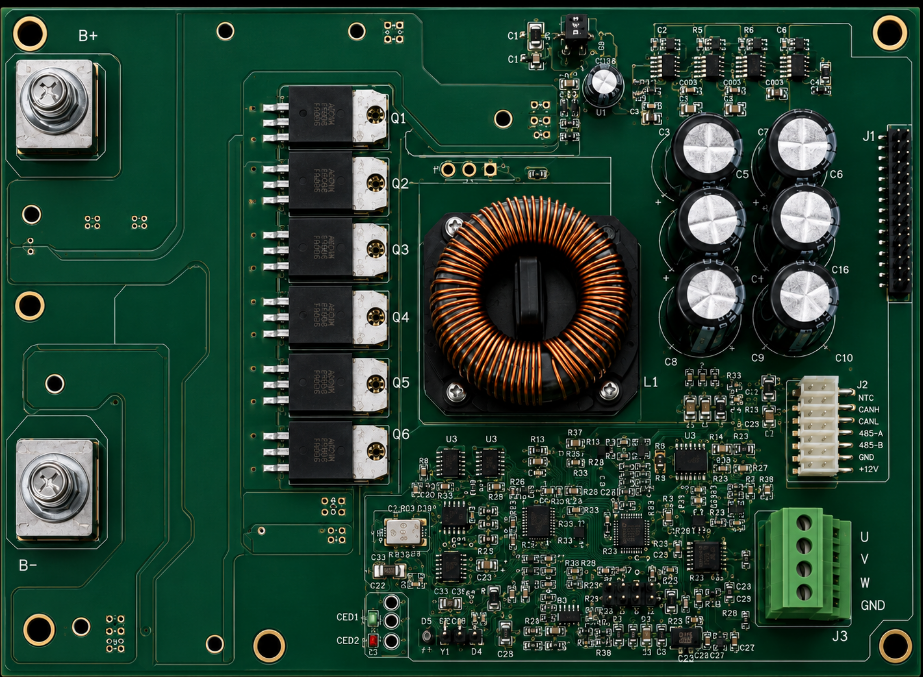
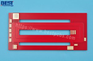
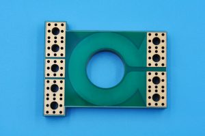
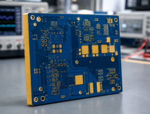
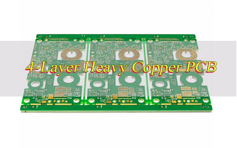
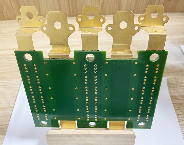
Heavy copper PCB for power electronics is used in circuits that carry high current, generate heat, or operate under repeated load changes. It is common in power supplies, motor drives, inverters, battery systems, EV chargers, converters and industrial control modules.

This guide explains copper thickness, current capacity, thermal control, trace width, via design, stackup, fabrication risks, reliability testing, cost factors and supplier selection for heavy copper PCB projects.

Heavy Copper PCB for Power Electronics, https://www.bestpcbs.com/blog/2026/06/heavy-copper-pcb-for-power-electronics/

What Is Heavy Copper PCB for Power Electronics?

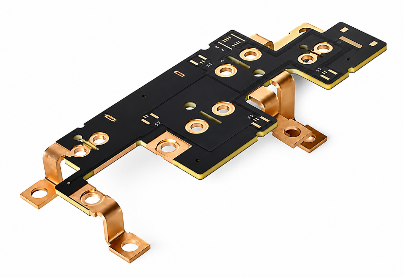
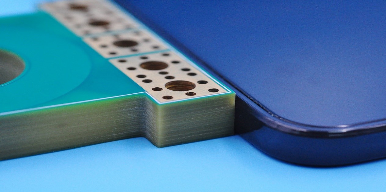
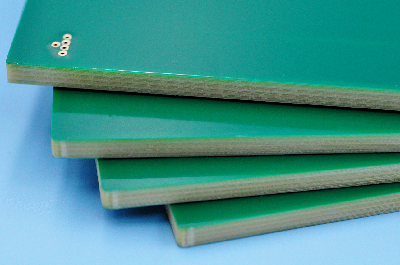
Heavy copper PCB for power electronics uses thicker copper than standard PCB to carry higher current and control heat. Standard PCB often uses 1 oz copper, while heavy copper PCB usually starts from 2 oz and can reach 3 oz, 4 oz, 6 oz or higher.

Thicker copper increases the conductor cross-section, which lowers resistance and reduces voltage drop. It also helps spread heat from MOSFETs, IGBTs, rectifiers, connectors and other power components.

Heavy copper PCB is commonly used in power supplies, motor drives, battery systems, converters and industrial control equipment. It is selected when standard copper cannot meet current load, thermal rise or mechanical reliability requirements.

Why Do Power Electronics Use Heavy Copper PCB?

Power electronics use heavy copper PCB because power circuits must carry current safely without excessive heat, voltage drop or conductor stress. Thin copper may work for control signals, but it is often not enough for high-current power paths.

Heavy copper improves three key areas: current carrying capacity, thermal spreading and mechanical strength. These points directly affect efficiency, reliability and service life in power conversion products.

Key functions include:

  • Carrying continuous and peak current with lower resistance
  • Reducing conductor temperature rise in compact layouts
  • Improving heat spreading near power semiconductors
  • Strengthening solder joints around connectors and terminals
  • Supporting long-duty operation in industrial environments
  • Reducing failure risk during thermal cycling and vibration

For power electronics, copper thickness should be selected from real current, temperature rise and layout space, not from a fixed default value.

What Problems Does Heavy Copper PCB Solve in High-Current Circuits?

Heavy copper PCB solves failures caused by undersized conductors, weak heat spreading and poor power-path design. These problems often appear after prototype testing, thermal testing or early field operation.

The most common issue is localized overheating. It can occur near MOSFETs, rectifiers, terminals, narrow copper necks, via transitions or high-current connectors. Once heat concentrates in one area, solder joints, laminate and plated holes may degrade faster.

Heavy copper helps control:

  • Voltage drop across long or narrow power traces
  • Copper heating caused by high current density
  • Hot spots around switching and rectifier sections
  • Barrel cracking in stressed plated through holes
  • Pad lifting near high-current connectors
  • Solder joint fatigue under repeated load cycles

Heavy copper cannot correct poor circuit topology, weak airflow or unsuitable components. It must be used with correct layout, stackup, material and thermal design.

Where Is Heavy Copper PCB Used in Power Electronics Applications?

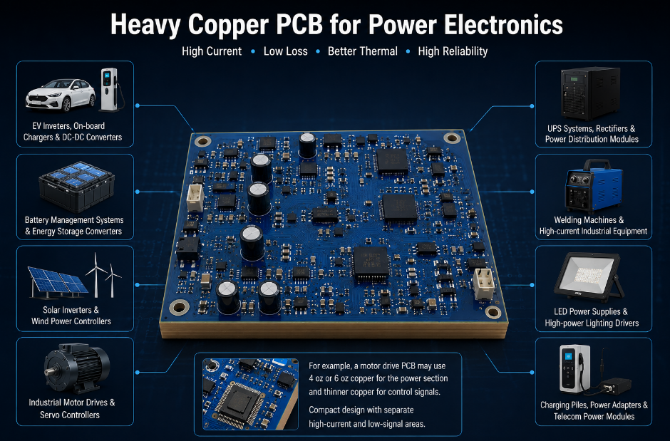
Heavy copper PCB for power electronics is used where current flow, switching loss and heat density are higher than standard PCB can handle. These applications often combine power devices, magnetic components, terminals and control circuits on one board.

Common applications include:

  • EV inverters, on-board chargers and DC-DC converters
  • Battery management systems and energy storage converters
  • Solar inverters and wind power controllers
  • Industrial motor drives and servo controllers
  • UPS systems, rectifiers and power distribution modules
  • Welding machines and high-current industrial equipment
  • LED power supplies and high-power lighting drivers
  • Charging piles, power adapters and telecom power modules

For example, a motor drive PCB may use 4 oz or 6 oz copper for the power section and thinner copper for control signals. This keeps the board compact while separating high-current and low-signal areas.

Heavy Copper PCB for Power Electronics, https://www.bestpcbs.com/blog/2026/06/heavy-copper-pcb-for-power-electronics/

What Copper Thickness Is Suitable for Power Electronics PCB?

Copper thickness depends on current, temperature rise, trace width, layer position, cooling method and board size. A higher copper weight does not automatically mean a better design. Oversized copper can increase cost, reduce spacing capability and make fabrication harder.

As a practical range, 2 oz copper is used for moderate power circuits, 3 oz–4 oz copper is common for high-current power boards, and 6 oz or above is used when current density is high or board space is limited.

CopperThicknessCommon Use
2 oz70 µmModerate current power PCB
3 oz105 µmLED drivers, converters, chargers
4 oz140 µmMotor drives, battery modules
6 oz210 µmHigh-current industrial power
10 oz+350 µm+Busbar-level power paths

Copper selection should be verified by trace width calculation, thermal simulation and prototype testing. For safety, check both continuous current and peak current, because many power products experience surge load during startup, switching or overload conditions.

How Does Heavy Copper PCB Improve Current Carrying Capacity?

Heavy copper PCB improves current carrying capacity by increasing the copper cross-section. A thicker copper path has lower resistance, which reduces heat generation and voltage drop under the same current load.

Key design points include:

  • Copper thickness affects current capacity directly. Common heavy copper options include 2 oz, 3 oz, 4 oz and 6 oz. Higher copper weight allows more current, but it also increases cost and fabrication difficulty.
  • Trace width must match real current load. A thick copper trace can still overheat if the width is too narrow. Designers should calculate continuous current, peak current and acceptable temperature rise before finalizing layout.
  • External layers usually dissipate heat better. Outer copper layers are closer to airflow, solder mask openings and heatsink contact areas, so they often carry heat away faster than internal layers.
  • Current bottlenecks must be avoided. Narrow copper necks near terminals, MOSFETs, fuses, connectors or shunt resistors can become hot spots even when the rest of the copper area is large.
  • Via transitions need enough current capacity. When current moves between layers, one or two small vias are usually not enough. Via arrays, larger hole sizes or plated slots may be required.
  • Connector ratings must match PCB current paths. The PCB copper may carry high current, but weak terminals, solder joints or connector pins can still limit the final design.

How Does Heavy Copper PCB Help Thermal Management?

Heavy copper PCB helps thermal management by reducing conductor loss and spreading heat across larger copper areas. It is especially useful in power electronics where MOSFETs, IGBTs, rectifiers, inductors and connectors generate concentrated heat.

Key thermal design points include:

  • Lower resistance reduces heat generation. Thicker copper creates a lower-resistance path, so less heat is produced when current flows through the PCB.
  • Large copper areas spread heat faster. Wide copper pours around power components help move heat away from local hot spots and reduce temperature concentration.
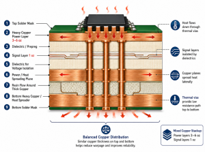
  • Thermal vias improve vertical heat transfer. Vias placed under or near hot pads can move heat to inner layers, bottom copper areas, heatsinks or metal base structures.
  • Hot components need direct heat paths. MOSFET drain pads, rectifier pads, power resistors and terminals should connect to copper areas that can transfer heat efficiently.
  • Copper balance helps temperature stability. Balanced copper distribution reduces warpage and supports more even heat spreading during operation.
  • Material selection still matters. High-Tg FR-4, CTI-rated laminate, IMS or other thermal materials may be required when working temperature or voltage stress is high.
  • Real load testing is necessary. Thermal simulation is useful, but final temperature rise should be checked under real current, enclosure and cooling conditions.

Heavy copper improves heat spreading, but it does not replace heatsinks, airflow, thermal pads or proper enclosure design in high-power systems.

What Materials Are Used for Heavy Copper PCB in Power Electronics?

Materials must support heat, insulation, copper adhesion and mechanical stress. Copper thickness is only one part of the design. If the laminate cannot handle temperature or voltage stress, the board may still fail.

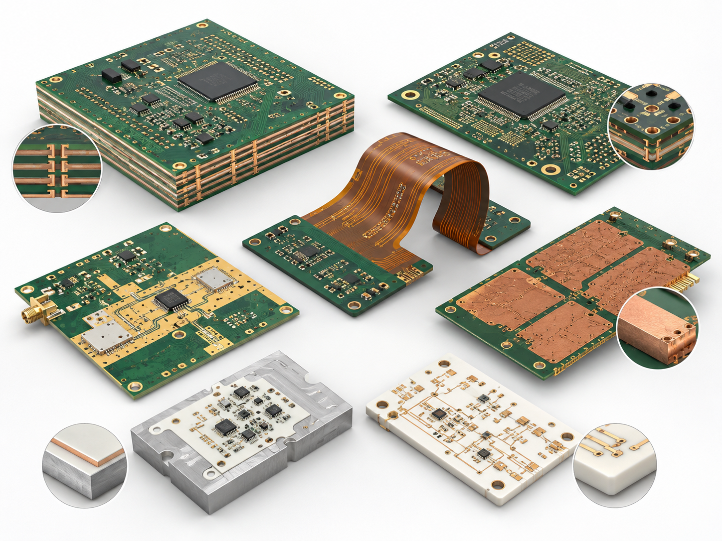
FR-4 is suitable for many industrial power boards. For higher temperature, higher voltage or stricter reliability requirements, designers may use High-Tg FR-4, CTI-rated laminate, IMS substrate or ceramic-filled material.

MaterialFeatureSuitable Project
High-Tg FR-4Better heat resistanceIndustrial power supplies
CTI-rated laminateImproved insulation safetyHigh-voltage power PCB
IMS substrateMetal-backed heat pathLED and power modules
Ceramic-filled laminateThermal and dimensional stabilityHigh-reliability power boards
Heavy copper foilHigh current pathMotor drives, converters
RoHS finishLead-free complianceEU and global projects

Material selection should match operating temperature, working voltage, insulation requirement, flame rating, assembly process and export compliance. For Europe and North America, RoHS, UL and customer-specific reliability requirements are often part of the procurement review.

How Should Trace Width and Spacing Be Designed for Heavy Copper PCB?

Trace width and spacing should be designed from current, voltage, copper thickness, temperature rise and fabrication capability. Heavy copper cannot follow the same spacing rules as standard 1 oz PCB because thick copper is harder to etch and control.

Key layout rules include:

  • Trace width should be based on current and temperature rise. Wider traces reduce resistance and help control heat. The design should consider continuous current, peak current and maximum allowed PCB temperature.
  • Spacing should be based on voltage and safety requirements. High-voltage circuits need enough clearance and creepage distance to prevent arcing, leakage current and insulation failure.
  • Copper thickness affects minimum spacing. As copper becomes thicker, etching becomes more difficult. Tight spacing between thick copper traces may increase undercut, short circuit or solder mask coverage risk.
  • Use copper pours for main power paths. Large copper pours are better than long narrow traces for high-current circuits because they reduce resistance and spread heat more evenly.
  • Avoid sharp corners and narrow necks. Sharp angles and sudden width changes can concentrate current and heat. Smooth transitions are better for power paths.
  • Separate power and signal areas. High-current switching paths can create noise. Sensitive signal traces should be kept away from MOSFET switching nodes, inductors and high-current loops.
  • Confirm limits before final layout. Minimum trace width, spacing, copper thickness and solder mask capability should be checked with the PCB manufacturer before Gerber release.

What Via Design Rules Apply to High-Current PCB?

Via design is critical in high-current PCB because vias must carry current, transfer heat and withstand thermal stress. Poor via design can cause overheating, barrel cracking, uneven current sharing or failure during thermal cycling.

Key via design rules include:

  • Use via arrays for high-current transfer. One small via is rarely enough for a power path. Multiple vias should be used when current moves between copper layers.
  • Increase finished hole size when possible. Larger vias provide more plating area and better current capacity. They also improve mechanical strength compared with very small vias.
  • Check finished copper plating thickness. Via reliability depends on actual plated hole wall thickness, not only drill size. Cross-section inspection is useful for heavy copper PCB.
  • Place vias close to the current path. Power vias should be located near terminals, MOSFETs, rectifiers and other high-current areas to reduce path length and resistance.
  • Use thermal vias under hot components. Thermal vias can move heat from top copper to bottom copper, internal copper planes or heatsink contact areas.
  • Avoid using signal vias as power vias. Small signal vias are not designed for high current and may create localized heating or early failure.
  • Consider plated slots for terminals. For very high-current connectors or press-fit terminals, plated slots may provide stronger current transfer and mechanical support than small round vias.
  • Keep via arrays balanced. Uneven via placement can cause unequal current sharing and local overheating. Symmetrical via groups usually perform better.

How Should Stackup and Copper Balance Be Planned?

Stackup and copper balance should be planned before layout is finalized. In heavy copper PCB fabrication, poor copper balance can cause warpage, uneven lamination pressure, soldering defects and unstable assembly yield.

Key planning rules include:

  • Keep copper distribution balanced. Avoid placing a large heavy copper area on one layer while the opposite layer has very little copper. Uneven copper can pull the board during lamination and reflow.
  • Separate power and signal functions. High-current layers should be kept away from sensitive analog, communication or control signals when possible. This reduces noise coupling and improves layout stability.
  • Use proper dielectric thickness for voltage insulation. High-voltage power electronics may require larger spacing between copper layers to prevent breakdown and leakage risk.
  • Place return paths close to switching current paths. Short return paths help reduce loop area, switching noise and electromagnetic interference in converters, motor drives and inverters.
  • Confirm finished copper thickness. Base copper and plated copper are not the same. Buyers should confirm the final copper thickness after plating, especially for 3 oz, 4 oz and 6 oz boards.
  • Review stackup before Gerber release. Stackup changes after layout may affect trace width, impedance, spacing, via structure and production cost.

Case example:
A motor drive PCB used 4 oz copper on outer power layers and thinner copper for control routing. The first layout had large copper pours only on the top layer, which caused warpage risk during assembly. After DFM review, copper was redistributed across opposite layers, return paths were adjusted, and thermal vias were added near MOSFET areas. The revised stackup improved flatness, heat distribution and batch production stability.

What Manufacturing Challenges Affect Heavy Copper PCB Fabrication?

Heavy copper PCB fabrication is more difficult than standard PCB production because thick copper affects etching, plating, lamination, drilling and solder mask application. These process risks should be reviewed during DFM before tooling.

Common manufacturing challenges include copper undercut, uneven plating, resin voids, poor solder mask coverage, warpage, hole wall defects and dimensional drift. The risk becomes higher when copper thickness increases or when trace spacing is too tight.

Main control points include:

  • Adjust trace spacing for thick copper etching
  • Balance copper distribution across the panel
  • Control resin flow during lamination
  • Improve plating uniformity in vias and through holes
  • Apply suitable solder mask thickness around copper steps
  • Inspect cross-sections for plating and lamination quality
  • Run thermal stress tests for high-reliability projects

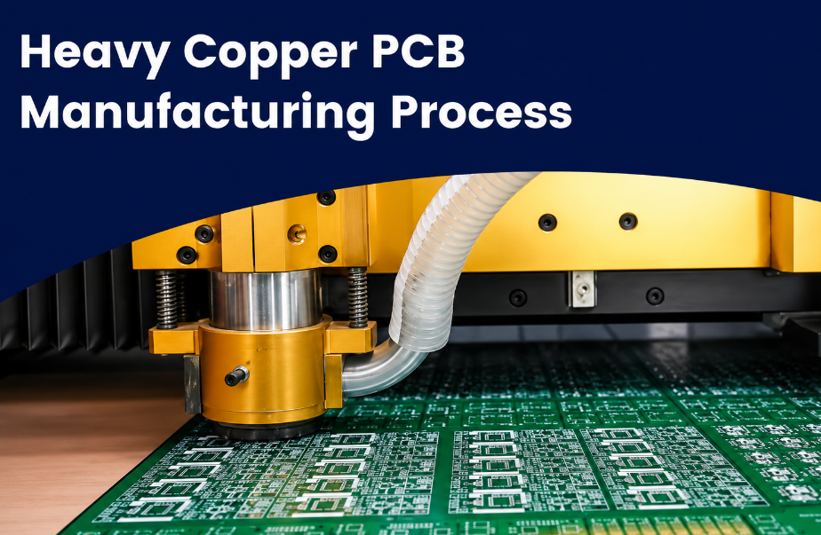
A practical process flow starts with DFM review, then material preparation, inner layer imaging, etching, lamination, drilling, copper plating, outer layer imaging, final etching, solder mask, surface finish, routing, electrical testing and final inspection.

What Quality Tests Are Needed for Heavy Copper PCB Reliability?

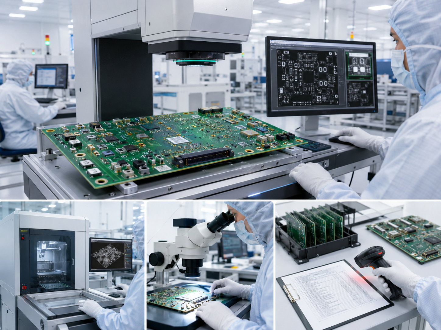
Heavy copper PCB should be tested for copper thickness, plated hole quality, electrical continuity, solderability, thermal resistance and final dimensions. Thick copper boards carry higher current, so hidden defects can become serious reliability risks during operation.

Important quality tests include:

  • AOI inspection. Checks open circuits, shorts, conductor shape, over-etching, under-etching and pattern defects before shipment.
  • 100% electrical testing. Confirms circuit continuity and insulation performance. This is required for high-current PCB because open or short defects can damage power modules.
  • Copper thickness measurement. Verifies whether finished copper meets the required specification, such as 2 oz, 3 oz, 4 oz or 6 oz.
  • Cross-section inspection. Checks hole wall plating thickness, copper bonding, resin filling, lamination quality and possible barrel defects.
  • Thermal stress testing. Exposes the PCB to heat stress to check delamination, blistering, hole wall cracking and laminate stability.
  • Solderability testing. Confirms whether pads and terminals can be soldered properly during assembly, especially after storage or surface finish processing.
  • Ionic contamination testing. Checks whether chemical residues remain on the board. Excessive residue may cause leakage, corrosion or reliability problems.
  • Dimensional inspection. Verifies board outline, slot size, hole position, thickness and tolerance before assembly.
  • Visual inspection. Reviews solder mask coverage, copper exposure, surface finish quality, scratches, dents and edge defects.
  • Final quality report. For power electronics projects, buyers can request inspection data for copper thickness, cross-section, electrical testing and thermal stress results.
Heavy Copper PCB for Power Electronics, https://www.bestpcbs.com/blog/2026/06/heavy-copper-pcb-for-power-electronics/

What Factors Affect Heavy Copper PCB Cost?

Heavy copper PCB cost is affected by copper weight, layer count, board size, material grade, hole density, copper balance, surface finish, tolerance, testing and order quantity. The thicker the copper, the higher the material cost and process difficulty.

Cost also increases when the design has tight spacing, dense vias, specialty laminate, ENIG finish, strict cross-section requirements or low-volume production. For very thick copper, fabrication time and yield risk become important pricing factors.

Main cost factors include:

  • Copper thickness and finished copper requirement
  • Board layer count and stackup complexity
  • High-Tg, CTI-rated or specialty laminate
  • Minimum trace width and spacing
  • Hole density, slot design and plating demand
  • Solder mask difficulty around thick copper
  • ENIG, HASL lead-free or other surface finish
  • Cross-section, thermal stress and reliability tests
  • Prototype, small batch or volume production quantity

The lowest unit price is not always the lowest project cost. A poor design may cause overheating, failed samples, delayed approval or batch rejection. Heavy copper PCB cost should be reviewed with performance, yield and reliability risk together.

How to Choose a Heavy Copper PCB Manufacturer for Power Electronics?

Choose a heavy copper PCB manufacturer that can review current load, copper thickness, trace spacing, via capacity, stackup balance and testing requirements before production. Heavy copper projects require process control, DFM support and reliability testing, not only basic PCB fabrication.

Selection points include:

  • Check real heavy copper experience. The manufacturer should have experience with 2 oz, 3 oz, 4 oz, 6 oz or thicker copper for power electronics, motor drives, converters and industrial power modules.
  • Ask for DFM review before production. A qualified factory should check copper spacing, solder mask coverage, via structure, plating risk, stackup balance and possible warpage issues.
  • Confirm finished copper capability. The supplier should explain base copper, plated copper and final copper thickness clearly, not only quote a general copper weight.
  • Review testing capability. Cross-section inspection, electrical testing, copper measurement and thermal stress testing are important for heavy copper PCB reliability.
  • Check material and compliance support. For export projects, the manufacturer should support RoHS, UL-related material requirements, High-Tg laminate and IPC acceptance criteria when required.
  • Evaluate prototype-to-batch consistency. A good supplier should keep the same engineering data, material selection and process controls from sample approval to mass production.
  • Confirm communication speed. Heavy copper PCB often needs engineering clarification before production. Slow feedback can delay prototypes, testing and batch delivery.
  • Choose a real China source factory. EBest supports custom heavy copper PCB prototypes, small batches and volume production with global delivery, without claiming overseas factories, warehouses or local branches.
Heavy Copper PCB for Power Electronics, https://www.bestpcbs.com/blog/2026/06/heavy-copper-pcb-for-power-electronics/

FAQs About Heavy Copper PCB for Power Electronics

Q1: What is the minimum copper thickness for heavy copper PCB?

A1: Heavy copper PCB usually starts from 2 oz copper, which equals about 70 µm copper thickness. Many power electronics projects use 3 oz, 4 oz or 6 oz depending on current load, trace width, temperature rise and board size. The correct copper thickness should be calculated from actual electrical and thermal conditions.

Q2: Is thicker copper always better for power electronics PCB?

A2: No. Thicker copper can improve current capacity and heat spreading, but it also increases cost, etching difficulty and spacing limitations. A 6 oz board may not be necessary if 3 oz or 4 oz copper already meets the current and temperature targets. The best choice balances performance, manufacturability and cost.

Q3: Can heavy copper PCB be used with SMT assembly?

A3: Yes. Heavy copper PCB can support SMT assembly, but pad design, solder mask thickness and thermal balance must be checked carefully. Thick copper absorbs more heat during soldering, so reflow profile, solder paste volume and component thermal sensitivity should be reviewed before assembly.

Q4: What information should buyers provide before quoting?

A4: Buyers should provide Gerber files, drill files, stackup, copper thickness, board thickness, material, surface finish, quantity and testing requirements. For power electronics PCB, it is better to also provide working current, peak current, voltage, temperature rise target and operating environment.

Q5: Why does heavy copper PCB need DFM review?

A5: Heavy copper PCB needs DFM review because thick copper affects etching, plating, solder mask coverage, lamination and warpage control. DFM review can identify spacing risks, narrow copper necks, weak vias, poor copper balance and difficult solder mask areas before production starts.

Q6: What surface finish is commonly used for heavy copper PCB?

A6: ENIG, HASL lead-free, immersion tin and OSP can be used. ENIG is often selected for stable solderability and fine-pitch components, while HASL lead-free may be suitable for simpler power boards. The final choice depends on component type, storage time, soldering process, RoHS requirement and cost.

Q7: Can heavy copper PCB handle high voltage?

A7: Heavy copper PCB can be used in high-voltage power electronics, but voltage safety depends on clearance, creepage, dielectric thickness, material CTI and coating, not copper thickness alone. Designers should define working voltage, peak voltage and insulation requirement before layout.

Q8: Why do heavy copper PCB vias fail?

A8: Via failure is often caused by insufficient plating thickness, small via size, poor drilling quality, thermal cycling or excessive current concentration. High-current PCB should use suitable via diameter, via arrays, proper plating control and cross-section inspection to reduce barrel cracking and overheating risk.

Q9: Can heavy copper PCB reduce PCB temperature?

A9: Heavy copper can reduce conductor loss and heat concentration, but it cannot replace the full thermal system. High-power designs may still require heatsinks, airflow, thermal pads, metal baseplates or enclosure cooling. Final temperature should be tested under real current and working conditions.

Q10: What causes warpage in heavy copper PCB?

A10: Warpage is often caused by unbalanced copper distribution, uneven layer structure, high copper weight on one side, poor lamination control or unsuitable panel design. Balanced stackup and copper distribution are important for 4 oz, 6 oz and thicker copper boards.

Q11: Is heavy copper PCB suitable for prototypes?

A11: Yes. Heavy copper PCB prototypes are useful for checking current capacity, temperature rise, solderability, mechanical fit and assembly performance before batch production. Prototype testing can prevent redesign and reduce risk before larger power electronics orders.

Q12: What industries commonly use heavy copper PCB?

A12: Heavy copper PCB is widely used in EV chargers, battery systems, solar inverters, UPS systems, motor drives, welding machines, industrial power supplies, LED drivers and telecom power modules. These products usually require high current paths, stable heat spreading and stronger long-term reliability.

Q13: Can EBest manufacture custom heavy copper PCB?

A13: Yes. EBest supports custom heavy copper PCB manufacturing for prototypes, small batches and volume production. We can review copper thickness, stackup, trace width, spacing, via structure, solder mask coverage and testing requirements before production to help reduce project risk.

Heavy copper PCB for power electronics should be selected from real current load, voltage level, temperature rise, copper thickness, stackup and reliability requirements. A stable design depends on more than thick copper; trace width, spacing, via structure, material, solder mask and testing must work together.

If you need thick copper boards for power supplies, motor drives, inverters, battery systems, EV chargers or industrial power modules, EBest Circuit can support custom heavy copper PCB prototypes and batch production from China with global delivery. Send your Gerber files, stackup and technical requirements to sales@bestpcbs.com for a quotation.

You may also like

Fine-Line HDI PCB Design Guidelines & Manufacturing Process

June 16th, 2026

A fine-line HDI PCB is used for compact electronics that require fine-pitch components, microvias, dense routing and stable signal performance. It helps reduce board size while improving circuit density and reliability. This guide covers key design rules, trace width and spacing, materials, stackup, SAP vs mSAP, manufacturing process, quality testing, cost factors and supplier selection.

Are you worried about these problems in fine-line HDI PCB projects?

  • Design challenges: Fine line HDI PCB signal integrity challenges may appear when high-speed traces, fine-pitch BGA escape routing, microvias, impedance control, return paths and dense layer transitions are not planned correctly.
  • Prototype challenges: Small-batch fine-line HDI PCB prototype projects may face delayed engineering approval, material mismatch, microvia reliability concerns, line/space yield risk and repeated DFM corrections before production.
  • Assembly challenges: Dense BGA packages, via-in-pad structures, small solder mask openings and tight component spacing may increase solder wicking, bridging, voiding, warpage and inspection difficulty during PCB assembly.

As a 20+ years PCB manufacturer, EBest Circuit provides design review, prototype manufacturing and assembly support for global OEM projects, engineering teams and electronics brands.

  • Design solution: We review stackup, impedance, BGA fanout, microvia placement, trace spacing, reference planes and DFM rules before production to reduce signal loss, crosstalk, impedance deviation and redesign risk.
  • Prototype solution: We confirm materials, copper thickness, HDI build-up, laser microvia structure, via filling, surface finish and test requirements before fabrication to improve prototype accuracy and shorten approval cycles.
  • Assembly solution: We check via-in-pad filling, solder mask registration, BGA pad design, stencil opening, panelization and SMT inspection requirements before assembly to reduce solder defects and improve batch consistency.

Welcome to contact us if you have any request for HDI PCB design, prototype, manufacturing or assembly: sales@bestpcbs.com.

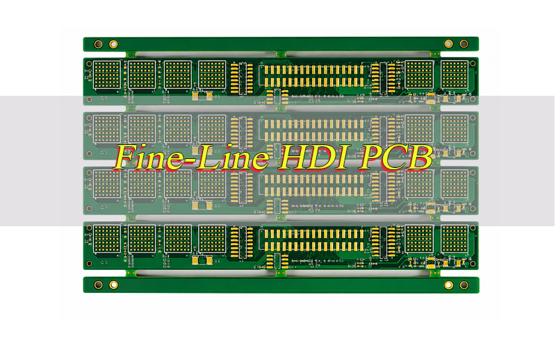
Fast-Line HDI PCB, https://www.bestpcbs.com/blog/2026/06/fine-line-hdi-pcb/

What Is a Fine-Line HDI PCB?

A fine-line HDI PCB is a high-density interconnect PCB built with narrow trace width, tight spacing, microvias, blind vias, buried vias and thin dielectric layers. It is designed for compact electronics where ordinary multilayer PCB routing cannot provide enough space.

It works by replacing large through-hole routing with laser microvias and short interconnection paths. This structure allows fine-pitch ICs, BGA packages, RF modules and high-speed interfaces to be routed in a smaller area.

The key value is higher circuit density with shorter signal paths. For products such as smartphones, 5G modules, medical devices, IoT sensors and compact industrial electronics, this structure helps reduce board size while keeping electrical performance stable.

What Are Advantages and Disadvantages of Fine Line HDI PCB?

Advanced fine line HDI PCB improves routing density and product miniaturization, but it also raises manufacturing difficulty. The design should balance space, signal speed, reliability, cost and production yield before using advanced fine-line rules.

Main advantages include:

  • Higher routing density for fine-pitch BGA, CSP and compact modules.
  • Smaller PCB size without reducing circuit functions.
  • Shorter signal paths for high-speed and RF circuits.
  • Lower via stub risk because microvias replace long through-hole transitions.
  • Better product integration for thin, lightweight and portable electronics.

Main limitations include:

  • Higher cost due to laser drilling, fine-line imaging and sequential lamination.
  • Stricter DFM rules for line width, spacing, annular ring and registration.
  • Higher yield risk if copper balance, lamination and via filling are not controlled.
  • Longer engineering review before prototype approval.
  • Less rework margin during SMT assembly because of dense layout and small pads.

Where Are Fine-Line HDI PCBs Commonly Used?

Fine-line HDI PCBs are used in electronics that require small size, high component density, stable signal transmission and reliable assembly. These products often contain fine-pitch ICs, RF sections, high-speed interfaces, sensors or compact mechanical structures.

Common applications include:

  • Smartphones, tablets and wearable electronics.
  • 5G modules, RF boards and communication devices.
  • Medical diagnostic devices, portable monitors and compact instruments.
  • IoT modules, smart sensors and wireless tracking products.
  • Automotive electronics, radar modules and control units.
  • Industrial controllers, compact power modules and robotics boards.
  • Flexible and rigid-flex projects for limited-space designs.

Fine-line HDI PCB applications in smartphones are especially common because smartphones use dense BGA chips, RF modules, camera modules, antennas, battery management circuits and high-speed data interfaces in a very limited internal space.

What Is the Difference Between Fine-Line and Standard HDI PCB?

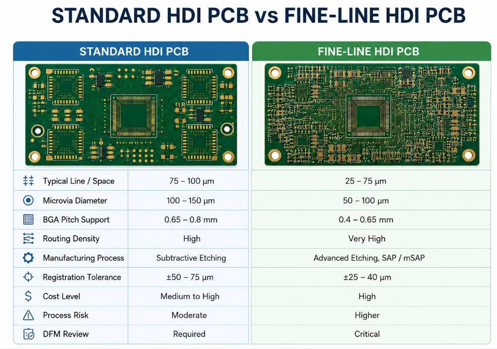
A standard HDI PCB already uses microvias and higher routing density than a conventional multilayer PCB. A fine-line HDI PCB goes further by using narrower line/space, tighter registration, more precise imaging and more controlled plating.

ItemStandard HDI PCBFine-Line HDI PCB
Typical line/space75–100 μm25–75 μm
Common processSubtractive etchingAdvanced etching, SAP or mSAP
Microvia size100–150 μm50–100 μm
BGA support0.65–0.8 mm pitch0.4–0.65 mm pitch
Routing densityHighVery high
Cost levelMedium to highHigh
Process riskModerateHigher
DFM reviewRequiredCritical

The core difference is manufacturing tolerance. Fine-line structures leave less process margin, so stackup, copper thickness, line compensation, lamination and inspection should be confirmed before layout is finalized.

Fine-Line vs Standard HDI PCB, https://www.bestpcbs.com/blog/2026/06/fine-line-hdi-pcb/

What Minimum Trace Width and Spacing Can Fine-Line HDI PCB Support?

Fine-line HDI PCB minimum trace width and spacing can commonly support 75/75 μm, 50/50 μm or 25/25 μm line and space, depending on copper thickness, process route, material, layer count and production volume. Smaller line/space does not always mean better design.

CapabilityPractical Range
Standard HDI line/space75/75 μm to 100/100 μm
Advanced fine line50/50 μm to 75/75 μm
Ultra fine line25/25 μm to 50/50 μm
Laser microvia diameter50–150 μm
Microvia aspect ratio0.75:1 preferred, 1:1 max
Controlled impedance tolerance±5% to ±10%
BGA pitch support0.4 mm to 0.8 mm
Finished copper12 μm to 35 μm typical

The safest choice is not always the smallest trace. For better yield and cost control, use fine-line rules only in high-density areas such as BGA escape, and keep other routing areas wider when space allows.

What Technical Parameters Should Be Confirmed Before Fine-Line HDI PCB Design?

Before fine-line HDI PCB design, confirm line width, spacing, microvia size, dielectric thickness, copper weight, impedance, BGA pitch, surface finish and reliability class. These parameters affect routing density, yield, testability and price.

ParameterRecommended Check
Layer count4–16 layers based on routing density
HDI structure1+N+1, 2+N+2, stacked or staggered
Line/space25/25 μm to 100/100 μm
Microvia50–150 μm laser drilled
Via fillingCopper filling for via-in-pad or stacked vias
Copper weight0.5 oz to 1 oz for fine-line layers
Dielectric thickness50–100 μm common for build-up layers
Impedance50Ω single-ended, 90Ω or 100Ω differential
Surface finishENIG, ENEPIG, immersion silver or OSP
StandardsIPC-2226, IPC-6012, IPC-A-600, RoHS

Early parameter confirmation prevents redesign. Once BGA fanout, stackup and impedance are fixed, late changes may affect the whole PCB layout, drill plan, lamination structure and assembly result.

What Substrate Materials Are Used in Fine-Line HDI PCB?

Fine line HDI PCB substrate materials should support laser drilling, stable lamination, low dielectric loss, dimensional stability and reliable copper adhesion. Material selection depends on signal speed, thermal stress, layer count and product environment.

Common substrate materials include:

  • High-Tg FR-4: Suitable for many industrial, IoT and consumer products.
  • Low-Dk/low-Df laminate: Better for high-speed, RF, 5G and low-loss signal transmission.
  • Halogen-free laminate: Used when environmental compliance is required.
  • BT resin or advanced build-up material: Used for fine pitch and very high-density structures.
  • Flexible polyimide: Used in flexible fine-line HDI PCB and rigid-flex projects.

For high-speed designs, material loss matters as much as routing density. A low-Df laminate helps reduce insertion loss, while stable CTE helps reduce microvia cracking during reflow and thermal cycling.

How Should Fine-Line HDI PCB Stackup Be Designed?

A fine-line HDI PCB stackup should be designed around routing density, microvia structure, impedance control, power integrity, copper balance and assembly flatness. The stackup should be confirmed before PCB layout begins because BGA escape routing, dielectric thickness, drill pairs and impedance values are all connected.

A good stackup gives high-speed traces a stable reference plane, keeps microvias short, reduces via stubs and improves lamination reliability. For fine-pitch BGA, the most common HDI structures are 1+N+1 and 2+N+2, depending on routing density and layer count.

Example: 8-layer fine-line HDI PCB stackup for compact high-speed electronics

LayerFunctionDesign Notes
L1Component + signalBGA escape, short high-speed routing, microvia to L2
L2Ground planeContinuous reference plane for L1
L3SignalControlled impedance routing
L4Power planeMain power distribution
L5Ground planeReturn path and shielding
L6SignalHigh-speed or control signal routing
L7Ground or power planeReference plane for L8
L8Component + signalBottom-side components and routing

Key stackup rules:

  • Use continuous ground planes near high-speed layers. This helps reduce impedance variation, crosstalk and EMI risk.
  • Keep microvias short and manufacturable. Laser microvias are usually used between adjacent layers, such as L1-L2 or L8-L7.
  • Avoid unnecessary stacked microvias. Stacked vias save space but increase plating and reliability risk.
  • Use staggered microvias when possible. They are often easier to manufacture and more stable for thermal cycling.
  • Balance copper on both sides. Uneven copper distribution may cause warpage during lamination, reflow or assembly.
  • Confirm dielectric thickness early. Dielectric thickness directly affects impedance, trace width and routing rules.
  • Separate noisy power areas from sensitive signals. RF, high-speed digital and analog sections should have clean return paths.

For most fine-line designs, the safest approach is to use fine-line rules only where routing density requires them. BGA escape areas may use 50/50 μm or smaller line/space, while less dense areas can use wider traces to improve yield and reduce cost.

Fine-Line HDI PCB Design Guidelines and Considerations

This design work should follow a clear engineering sequence. The goal is to prevent routing failure, signal integrity problems, microvia reliability issues and assembly defects before production starts.

Step 1: Confirm manufacturing capability before layout.
Before routing, confirm the manufacturer’s minimum line width, spacing, laser microvia size, copper thickness, via filling capability, solder mask registration and impedance tolerance. Do not rely only on CAD default rules.

Step 2: Define the BGA escape strategy.
For 0.4 mm, 0.5 mm or 0.65 mm pitch BGA packages, choose dog-bone fanout, via-in-pad, blind vias or microvias based on available routing channels. If via-in-pad is used, confirm copper filling and planarization before assembly.

Step 3: Build the stackup around signals and return paths.
High-speed traces should route over continuous ground planes. Avoid routing critical signals across split planes, voids or layer transitions without nearby ground stitching vias.

Step 4: Control impedance from the beginning.
Single-ended and differential impedance should be calculated before layout. Common targets include 50Ω single-ended, 90Ω differential and 100Ω differential, depending on the interface.

Step 5: Reduce fine-line routing only to critical areas.
Use the smallest line/space only in BGA breakout or dense routing zones. Wider routing in open areas improves manufacturing yield and cost control.

Step 6: Manage microvia reliability.
Keep laser microvias on adjacent layers when possible. Avoid deep microvias, excessive stacked vias and unsupported via structures. For stacked microvias, copper filling quality should be confirmed.

Step 7: Protect signal integrity.
Fine line HDI PCB signal integrity challenges often come from impedance mismatch, long parallel traces, poor return paths, dense via transitions and weak grounding. Keep high-speed traces short, matched and referenced to solid planes.

Step 8: Check solder mask and pad design.
Fine-pitch pads require accurate solder mask opening and registration. Poor solder mask control may cause solder bridging, insufficient solder or BGA assembly defects.

Step 9: Plan assembly before fabrication.
Via-in-pad, BGA pitch, stencil thickness, component spacing, panelization and inspection method should be reviewed before PCB manufacturing. Dense HDI boards leave little room for SMT rework.

Step 10: Run DFM review before prototype.
A DFM review should check line/space, annular ring, drill-to-copper clearance, copper balance, impedance coupon, solder mask clearance, surface finish and panel design. This step reduces engineering questions and prototype delays.

SAP vs mSAP in Fine-Line HDI PCB: Which Process Should You Choose?

SAP and mSAP are advanced processes used when traditional subtractive etching cannot hold very fine line and spacing with stable yield. For most fine-line HDI PCB projects, the decision depends on target line/space, copper thickness, routing density, cost target and production volume.

ItemSAPmSAP
Full NameSemi-Additive ProcessModified Semi-Additive Process
Main PrincipleBuilds copper traces from a very thin seed layerUses a thin base copper layer and selective copper plating
Typical Line/SpaceBelow 25/25 μm in advanced applications25/25 μm to 50/50 μm commonly used
Best ForUltra-fine substrate-like structuresFine-line HDI PCB and compact electronic modules
Copper ControlVery precisePrecise and more practical for PCB production
Cost LevelHigherLower than SAP in many HDI projects
Production DifficultyVery highHigh but more widely used
Yield RiskHigh if process control is weakMore stable for many fine-line HDI projects
ApplicationIC substrates, ultra-dense packaging, advanced modulesSmartphones, wearable devices, 5G modules, medical electronics
When to ChooseWhen ultra-fine line/space is requiredWhen traditional etching cannot meet fine-line HDI routing needs

Choose SAP when the design requires extremely fine traces close to substrate-level density. It is suitable for advanced miniaturized electronics where normal HDI PCB manufacturing cannot meet the routing requirement.

Choose mSAP when the project needs fine-line HDI PCB routing, high BGA density and better line control without moving to the highest-cost substrate process. It is often a practical choice for 25/25 μm to 50/50 μm line/space.

For many commercial fine-line projects, mSAP offers a better balance between density, manufacturability, cost and production stability. However, the final choice should be confirmed by line/space, copper thickness, layer structure and batch quantity.

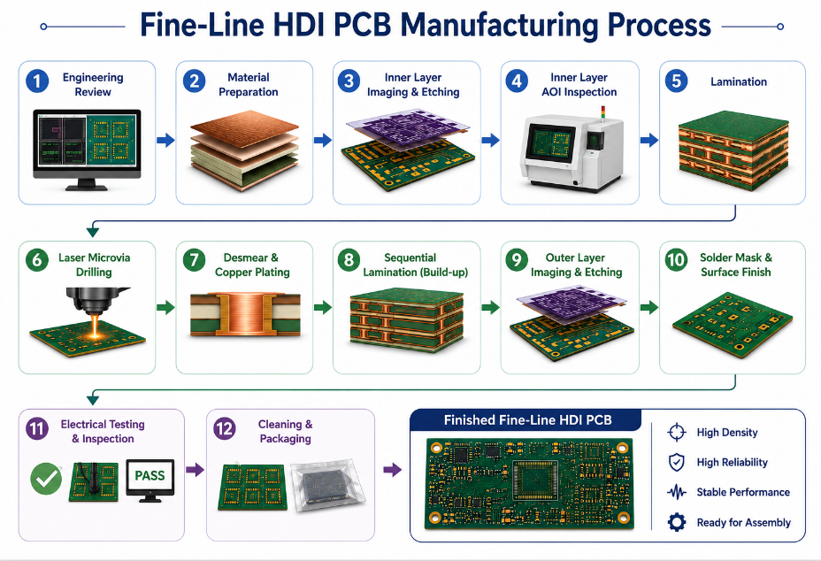
How Does the Fine-Line HDI PCB Manufacturing Process Work?

The fine-line HDI PCB manufacturing process requires tighter control than standard multilayer PCB production. Each step affects trace accuracy, microvia reliability, impedance and final assembly yield.

Step 1: Engineering review
The manufacturer reviews Gerber files, drill files, stackup, material, copper thickness, impedance requirement, line/space, BGA pitch, HDI structure and surface finish. This step confirms whether the design matches real production capability.

Step 2: Material preparation
The selected laminate, copper foil, prepreg and build-up materials are prepared according to the approved stackup. For high-speed products, low-Dk and low-Df materials may be used to reduce signal loss.

Step 3: Inner layer imaging and etching
The inner layers are coated, exposed, developed and etched. Fine-line imaging requires accurate pattern transfer and strict etching compensation to prevent line width loss, open circuits or copper residue.

Step 4: Inner layer inspection
AOI checks the inner layer pattern before lamination. This is important because inner layer defects cannot be repaired after the stackup is pressed together.

Step 5: Lamination
Core layers, prepreg and copper foil are laminated under controlled heat and pressure. Fine-line HDI PCB lamination must control resin flow, copper balance, dimensional stability and layer registration.

Step 6: Laser microvia drilling
Laser drilling forms microvias between adjacent layers. The process must control via diameter, depth, position accuracy and dielectric removal to ensure reliable plating.

Step 7: Desmear and copper plating
The drilled microvias are cleaned and prepared for metallization. Copper plating builds electrical connection through the vias. For via-in-pad and stacked microvias, copper filling may be required.

Step 8: Sequential lamination
For 1+N+1 or 2+N+2 HDI structures, laser drilling, plating and lamination may be repeated. More build-up layers increase routing density but also raise cost and process risk.

Step 9: Outer layer imaging and fine-line etching
The outer layers are imaged and etched with tight process control. If the design uses mSAP or SAP, selective copper build-up and flash etching are used to form finer traces.

Step 10: Solder mask and surface finish
Solder mask is applied to protect copper and define pads. Then surface finish such as ENIG, ENEPIG, OSP or immersion silver is applied based on assembly and reliability requirements.

Step 11: Electrical testing and final inspection
The boards go through E-test, AOI, impedance test, dimensional inspection and appearance check. For high-density designs, X-ray or cross-section checks may also be used.

Step 12: Packaging or assembly preparation
Finished boards are cleaned, packed and prepared for shipment or SMT assembly. If assembly is required, panelization, stencil design, BGA inspection and component placement files are reviewed before production.

Fine-Line HDI PCB Manufacturing Process, https://www.bestpcbs.com/blog/2026/06/fine-line-hdi-pcb/

What Quality Tests Are Required for Fine-Line HDI PCB Manufacturing?

Fine-line HDI PCB quality testing should focus on fine trace accuracy, microvia reliability, impedance stability, surface finish and assembly readiness. Because the line/space is very small, minor defects may cause open circuits, shorts, soldering defects or field failure.

  • Material inspection
    Check laminate, copper foil, prepreg, build-up material and material lot before production. Stable materials help control lamination, impedance and microvia reliability.
  • AOI inspection
    AOI checks fine traces, spacing, copper residue, opens, shorts and pattern distortion. Inner layer AOI is especially important because hidden defects cannot be repaired after lamination.
  • Lamination inspection
    Check board thickness, layer registration, resin flow, copper balance and warpage. Poor lamination may cause delamination, layer shift or microvia cracking.
  • Microvia inspection
    Check laser microvia diameter, depth, position and cleanliness. Poor laser drilling may lead to plating voids, weak connections or reliability risks.
  • Plating and via filling inspection
    Check copper plating thickness, via wall quality and filling condition. For via-in-pad and stacked microvias, poor filling may cause voids, solder wicking or BGA soldering defects.
  • Cross-section analysis
    Cross-section checks copper thickness, microvia filling, via wall quality and interlayer connection. It is useful for high-reliability fine-line HDI PCB projects.
  • Electrical testing
    100% E-test checks circuit continuity and insulation. It helps find tiny opens and shorts that may not be visible during appearance inspection.
  • Impedance testing
    Controlled impedance coupons should be tested for high-speed designs. Common tolerance is ±5% to ±10%, depending on the project requirement.
  • X-ray inspection
    X-ray checks hidden via filling, stacked microvia alignment and via-in-pad structures. It is useful for dense HDI designs with internal connection risks.
  • Solderability and surface finish inspection
    Check ENIG, ENEPIG, OSP or immersion silver for thickness, oxidation, contamination and pad flatness. Good surface finish improves fine-pitch SMT assembly quality.
  • Warpage and final inspection
    Check board flatness, dimensions, solder mask, silkscreen, cleanliness, quantity and packing before shipment. Flatness is especially important for BGA and thin HDI boards.

These tests help reduce open circuits, short circuits, microvia failure, impedance deviation, soldering defects and batch quality risks. For this manufacturing work, quality control should run through the whole process, not only the final inspection.

What Factors Affect Fine-Line HDI PCB Cost?

Cost is mainly affected by line/space, layer count, lamination cycles, microvia structure, material grade, via filling, impedance control, inspection level and delivery urgency. Board size alone does not decide price.

Cost FactorCost Impact
Line/space below 75/75 μmHigher imaging and yield cost
2+N+2 or higher HDIMore lamination cycles
Stacked microviasHigher drilling and filling cost
Via-in-pad copper fillingHigher plating and planarization cost
Low-Dk materialHigher laminate cost
ENEPIG finishHigher surface finish cost
Controlled impedanceCoupon and test cost
Small batch prototypeHigher unit price
Urgent lead timeHigher production scheduling cost

To control cost, avoid over-design. Use the finest line only in BGA escape or high-density zones, and keep other areas at wider rules when board space allows.

How to Choose Reliable Fine-Line HDI PCB Manufacturers?

Fine line HDI PCB manufacturers should provide more than fabrication. The supplier should help review the design, control advanced processes, test critical structures and support prototype-to-mass-production transition.

Key selection points include:

  • Check real fine-line capability.
    Ask for production-level line/space capability, not only laboratory capability. A manufacturer may claim 25/25 μm, but stable batch production may require different design rules.
  • Confirm HDI build-up experience.
    The supplier should understand 1+N+1, 2+N+2, stacked microvias, staggered microvias, blind vias, buried vias and via-in-pad structures.
  • Review laser drilling control.
    Laser microvia diameter, depth, taper, registration and cleanliness directly affect plating reliability. Poor microvia control may cause intermittent failure after thermal stress.
  • Check via filling and planarization ability.
    For fine-pitch BGA, via-in-pad usually requires copper filling and flat pad surfaces. Poor filling may cause solder wicking, voids or weak BGA joints.
  • Ask for stackup and impedance support.
    A reliable supplier should help check dielectric thickness, copper weight, material Dk/Df, impedance calculation and reference plane structure before production.
  • Confirm etching capability.
    If the design uses 50/50 μm or smaller line/space, the manufacturer should explain the suitable mSAP route, HDI PCB fine line etching capability, copper thickness limit and expected yield.
  • Check inspection equipment.
    AOI, E-test, X-ray, cross-section, impedance testing and solderability testing are important for fine-line HDI PCB quality control.
  • Evaluate DFM response speed.
    Fine-line projects often require engineering questions before production. Slow feedback may delay prototype approval and affect product launch.
  • Review assembly experience.
    If the project includes PCBA, the manufacturer should understand BGA assembly, stencil design, via-in-pad, solder mask registration, warpage control and functional testing.
  • Confirm standards and compliance.
    Ask whether the supplier can support IPC standards, UL, RoHS, customer quality reports and export documentation according to project needs.
  • Check prototype and mass production consistency.
    The process used for prototype should be scalable to mass production. Otherwise, the first batch may pass while later batches face yield or cost problems.
  • Avoid choosing only by low price.
    Fine-line board failures can cause redesign, delivery delay, assembly scrap and field return. A slightly lower quote may cost more if process control is weak.

The best manufacturer should provide clear engineering feedback before production, not only accept files and quote quickly. For advanced fine-line designs, early technical communication is one of the strongest indicators of supplier reliability.

Why Choose EBest for Fine-Line HDI PCB Manufacturing?

EBest Circuit provides design review, prototype, mass production, component sourcing and PCB assembly support. For customers, this helps reduce communication cost, engineering errors and production delay.

  • One-stop PCB and PCBA service
    EBest supports PCB design, prototype, mass production, component sourcing and assembly. Customers can manage the project through one supplier instead of coordinating several vendors.
  • 20+ years of manufacturing experience
    Founded in 2006, EBest has long-term experience in custom PCB manufacturing. This helps customers identify stackup risks, line/space limits, microvia issues and assembly concerns before production.
  • Prototype to mass production support
    EBest can support small-batch prototypes and batch production. Customers can verify the design first, improve DFM details and then move to volume manufacturing with a more stable process.
  • Wide PCB manufacturing capability
    EBest manufactures HDI PCB, multilayer PCB, FR4 PCB, high frequency PCB, high speed PCB, impedance control PCB, flexible PCB, rigid-flex PCB, ceramic PCB, metal core PCB and heavy copper PCB. This is useful for projects involving HDI, RF, high-speed or thermal requirements.
  • Fine-line HDI engineering review
    Fine-line designs often involve dense BGA routing, narrow trace spacing, laser microvias, via-in-pad and impedance control. EBest reviews these details before production to reduce redesign and prototype failure risk.
  • Stable production capacity
    EBest has a monthly capability of 260,000 square feet, around 28,900 square meters. This helps customers handle prototype orders, repeat orders and growing production demand.
  • Quick-turn support for urgent projects
    For urgent boards, EBest can provide expedited service, and qualified urgent projects can be shipped within 24 hours. This helps engineering teams shorten validation and testing cycles.
  • Certified quality system
    EBest holds ISO 9001:2015, IATF 16949, ISO 13485:2016, AS9100D, UL, RoHS and REACH certifications. These certifications support customers in automotive, medical, aerospace, industrial and export projects.
  • Support for high-speed and impedance control designs
    This board type is often used in compact high-speed products. EBest helps review signal layers, reference planes, dielectric thickness and impedance targets before manufacturing.
  • Assembly support for dense layouts
    EBest reviews BGA pads, via-in-pad filling, solder mask registration, stencil openings and component spacing before assembly. This helps reduce solder bridging, solder wicking, voiding and rework risk.
  • China source factory with global supply
    EBest provides custom PCB and PCBA solutions for global OEM and ODM customers. Customers can use EBest for prototype, manufacturing and assembly without relying on multiple middle suppliers.
Fine-Line HDI PCB, https://www.bestpcbs.com/blog/2026/06/fine-line-hdi-pcb/

FAQs About Fine Line HDI PCB

Q1: When should I use a fine-line HDI PCB instead of a standard PCB?
A1: Use this board type when the design has fine-pitch BGA, limited board space, high signal density or strict size requirements. If a standard multilayer PCB cannot route all signals without increasing board size, microvias and narrow line/space can help improve routing density.

Q2: Is fine-line HDI PCB suitable for 0.4 mm BGA packages?
A2: Yes. This board type is commonly used for 0.4 mm BGA and compact IC packages. These designs often require laser microvias, via-in-pad, tight solder mask registration and controlled pad flatness. The stackup and fanout method should be confirmed before PCB layout starts.

Q3: What is the common line width and spacing for fine-line HDI PCB?
A3: Common line/space includes 75/75 μm, 50/50 μm and 25/25 μm. The final value depends on copper thickness, layer count, material, process route and production quantity. For better yield, use the finest line only in dense routing areas.

Q4: Does fine-line HDI PCB always require mSAP or SAP?
A4: Not always. If the design uses 75/75 μm or similar rules, advanced subtractive etching may be enough. If the design requires 50/50 μm or below, mSAP may be more suitable. SAP is usually used for extremely fine substrate-like structures.

Q5: Why does fine-line HDI PCB cost more than standard HDI PCB?
A5: The cost is higher because this board requires tighter imaging, laser drilling, microvia plating, via filling, sequential lamination and more inspection steps. Cost also increases when the design uses stacked microvias, low-loss materials, controlled impedance or urgent prototype delivery.

Q6: What materials are commonly used for fine-line HDI PCB?
A6: Common materials include high-Tg FR-4, low-Dk/low-Df laminate, halogen-free laminate, BT resin and flexible polyimide. High-speed, RF and 5G products usually use low-loss materials. Flexible fine-line HDI PCB or rigid-flex structures may use polyimide-based materials.

Q7: Can fine-line HDI PCB be used for high-speed signals?
A7: Yes. This board can support high-speed signals when impedance, reference planes, return paths and via transitions are properly controlled. For DDR, USB, PCIe, RF or sensor interfaces, the design should avoid split planes, long stubs and uncontrolled layer transitions.

Q8: What causes signal integrity problems in fine-line HDI PCB?
A8: Signal integrity problems often come from impedance mismatch, poor return paths, long parallel routing, excessive via transitions, weak grounding or unsuitable materials. These risks increase in dense BGA areas, so stackup, dielectric thickness and routing rules should be reviewed before production.

Q9: Is via-in-pad necessary for fine-line HDI PCB?
A9: Via-in-pad is not always necessary, but it is often used for 0.4–0.65 mm BGA and compact layouts. It helps save routing space, but the via should be filled and planarized to prevent solder wicking, voids and poor BGA solder joints.

Q10: What tests are important for fine-line HDI PCB quality control?
A10: Important tests include AOI, E-test, X-ray, cross-section, impedance testing, solderability testing and final inspection. For this board type, microvia plating, via filling, line/space accuracy and impedance stability should be checked carefully before shipment or assembly.

Q11: What files should I prepare for fine-line HDI PCB quotation?
A11: Prepare Gerber files, drill files, stackup, material request, copper thickness, impedance requirements, surface finish, solder mask color, quantity, IPC class and delivery target. If assembly is required, also provide BOM, pick-and-place file and assembly drawings.

Q12: How can I reduce the cost of a fine-line HDI PCB project?
A12: Use fine-line rules only where routing density requires them, avoid unnecessary stacked microvias, choose practical materials and confirm the stackup early. Wider traces in open areas, simpler HDI build-up and clear DFM files can help reduce cost and improve production yield.

Q13: What should be checked before fine-line HDI PCB assembly?
A13: Before assembly, check BGA pad design, via-in-pad filling, solder mask opening, board flatness, surface finish, stencil thickness, panelization and component spacing. These checks help reduce solder bridging, solder wicking, BGA voiding, tombstoning and rework risk.

Q14: How do I choose a reliable fine-line HDI PCB manufacturer?
A14: Check real line/space capability, HDI build-up experience, laser drilling control, via filling quality, impedance testing, inspection equipment and assembly support. A reliable manufacturer should provide DFM feedback before production instead of only quoting from files.

Q15: Can EBest support fine-line HDI PCB prototype and assembly together?
A15: Yes. EBest Circuit supports fine-line HDI PCB design review, prototype, mass production, component sourcing and PCB assembly. This helps customers manage engineering review, bare board fabrication, component preparation and SMT assembly through one supplier.

Final Summary
This PCB structure is suitable for compact products with fine-pitch BGA, microvias, narrow trace spacing and high-speed signals. Before production, engineers should confirm stackup, material, impedance, microvia structure, surface finish and assembly requirements.

For buyers, a reliable supplier should provide DFM review, prototype support, stable manufacturing, quality testing and assembly coordination. This helps reduce redesign, delivery delay, soldering defects and batch quality risks.

EBest Circuit provides fine-line HDI PCB design review, prototype, mass production, component sourcing and PCB assembly. Send your files to EBest for a practical quotation: sales@bestpcbs.com.

You may also like

Custom 4-Layer Heavy Copper PCB Manufacturer for High-Current Power Applications

June 15th, 2026

A 4-layer heavy copper PCB is built for circuits that handle high current, high heat and long operating time. It uses thicker copper than standard PCB structures, so the board can support stronger power paths, lower resistance and better heat spreading.

EBest provides custom 4-layer heavy copper PCB manufacturing, prototype and assembly support for power electronics, industrial control, medical devices, aerospace modules, EV systems, energy storage and high-power equipment.

Are you worried about these problems in 4-layer heavy copper PCB projects?

  • Overheating risk: MOSFETs, terminals, relays, connectors and power ICs may generate local hot spots if the copper path is not designed correctly.
  • Voltage drop risk: Narrow current paths, weak via design or poor copper distribution may reduce power efficiency.
  • Manufacturing risk: Heavy copper increases etching difficulty, lamination stress, solder mask control and drilling requirements.
  • Assembly risk: Thick copper absorbs more heat during soldering, which may affect solder wetting and joint quality.

With 20+ years of PCB manufacturing experience, EBest provides 4-layer heavy copper PCB manufacturing and assembly solutions for global power electronics, industrial equipment and engineering projects.

  • Engineering review before production: Stackup, copper weight, current path, via structure and solder mask openings are checked before fabrication.
  • Controlled heavy copper production: Etching, lamination, drilling, plating and electrical testing are controlled throughout production.
  • Assembly process support: SMT process review, AOI inspection, functional testing and load-related inspection can be arranged based on project requirements.

If your project involves high current, tight reliability targets or strict production control, send your files to sales@bestpcbs.com for engineering review.

4-Layer Heavy Copper PCB

What Is a 4-Layer Heavy Copper PCB?

A 4-layer heavy copper PCB is a multilayer PCB with four conductive copper layers and thicker copper weight for high-current circuits. It is commonly used when standard 1 oz copper cannot safely carry the required current or manage heat.

In many projects, heavy copper starts from 2 oz to 3 oz, while higher-current boards may use 4 oz, 5 oz, 6 oz or more depending on the current path, board size and thermal target.

This structure allows engineers to separate power, ground, control and signal layers while keeping the board compact. For power electronics, this helps improve current flow, thermal stability and mechanical strength.

What Copper Thickness Is Common for a 4-Layer Heavy Copper PCB?

Copper thickness depends on current, temperature rise, trace width, board thickness and available routing space. For most 4-layer heavy copper PCB projects, copper weight usually ranges from 2 oz to 6 oz, while special power boards may require higher copper.

CopperThicknessCommon Use
2 oz70 µmMedium current power boards
3 oz105 µmIndustrial control and power modules
4 oz140 µmHigh-current power distribution
5 oz175 µmBattery systems and motor drivers
6 oz210 µmHigh-load power electronics
10 oz350 µmSpecial high-current applications

The best choice should be based on current load, allowed temperature rise, trace width and available PCB space, not only copper weight. Higher copper can carry more current, but it also increases spacing requirements, etching difficulty and production control requirements.

Why Choose a 4-Layer Heavy Copper PCB for High-Current Power Applications?

A 4-layer heavy copper PCB is chosen because it can carry higher current while keeping the layout more compact than a standard PCB. It also improves heat spreading and supports stronger power integrity.

Key advantages include:

  • Higher current capacity: Thick copper reduces resistance in power paths.
  • Better heat spreading: Larger copper mass helps move heat away from power components.
  • Compact power layout: Four layers allow better routing than single-sided or double-sided boards.
  • Improved reliability: Stronger copper paths reduce overheating and voltage drop.
  • Better mechanical strength: Heavy copper improves board durability in demanding equipment.

This PCB type is suitable when the product must operate safely under high load, vibration, heat or continuous power cycling.

Where Are 4 Layers Heavy Copper PCBs Commonly Used?

4-layer heavy copper PCBs are used in products that require stable current delivery, strong thermal performance and long-term reliability. They are common in power electronics and industrial equipment.

Common applications include:

  • Industrial control: Motor drives, power controllers, automation equipment and welding systems.
  • EV and energy systems: Battery management systems, charging modules and power distribution boards.
  • Medical equipment: Imaging power modules, surgical devices and diagnostic control boards.
  • Aerospace electronics: Power regulation modules, control units and high-reliability power boards.
  • Telecom power systems: Base station power modules and high-current conversion boards.
  • LED and lighting systems: High-power lighting drivers and thermal control boards.

For these industries, the board must support current, heat, insulation and reliability at the same time.

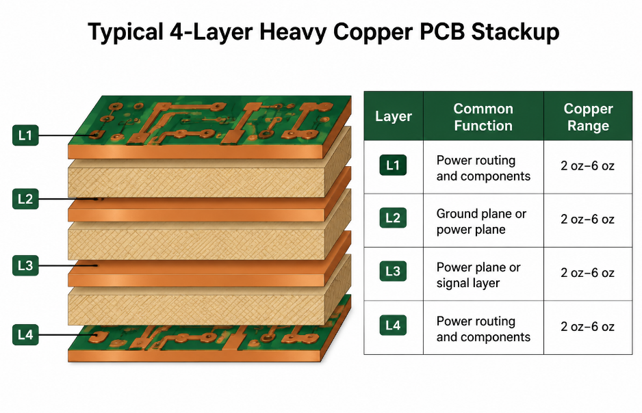
What Is the Typical 4-Layer Heavy Copper PCB Stackup?

A typical 4-layer heavy copper PCB stackup uses two outer copper layers and two inner copper layers. The stackup is usually designed to separate power, ground and signal functions while controlling heat and current flow.

LayerCommon FunctionCopper Range
L1Power routing and components2 oz–6 oz
L2Ground plane or power plane2 oz–6 oz
L3Power plane or signal layer2 oz–6 oz
L4Power routing and components2 oz–6 oz

A practical stackup may use outer layers for power components, inner layers for ground or current return, and thick copper planes for heat spreading. The final structure should match component placement, current direction and assembly requirements.

4-Layer Heavy Copper PCB Stackup

What Materials and Surface Finishes Are Used for 4-Layer Heavy Copper PCBs?

A 4-layer heavy copper PCB usually uses high-Tg FR4, heavy copper foil, reliable prepreg and a surface finish suitable for soldering. Material selection affects heat resistance, lamination quality and long-term stability.

ItemCommon OptionTypical Selection
Base materialHigh-Tg FR4Tg 150°C–180°C
Copper weight2 oz–6 ozHigher for power paths
Board thickness1.6 mm–3.2 mmBased on current and structure
Surface finishENIG, HASL, OSPBased on assembly needs
Solder maskHigh-temperature maskBetter insulation and protection
Finished copperIPC controlledBased on final performance target

ENIG is often selected for fine-pitch assembly and stable solderability. HASL can be used for less complex power boards, while OSP may suit selected SMT projects.

How to Design a 4-Layer Heavy Copper PCB for High Current?

Designing a 4-layer heavy copper PCB for high current starts with current flow, heat control and manufacturability. The layout should begin from the power path, return path, copper thickness and expected temperature rise.

Step 1: Confirm the current, voltage and temperature rise target.
Before layout, confirm the maximum current, continuous current, peak current, working voltage and allowed temperature rise. A board carrying 10A, 30A or 80A cannot use the same copper width, via quantity or connector design. If the current is continuous, the copper path must be more conservative than a short-pulse circuit.

Step 2: Choose the correct copper thickness for each layer.
For a custom 4-layer heavy copper PCB, common copper thickness includes 2 oz, 3 oz, 4 oz, 5 oz and 6 oz. Higher copper supports stronger current flow, but it also increases etching difficulty, spacing requirements and solder mask control. In many projects, outer layers carry high-current components, while inner layers work as power planes or ground return layers.

Step 3: Plan the stackup early.
A practical stackup should separate power, ground, control and signal functions. For example, L1 can carry power components and short high-current traces, L2 can work as a ground plane, L3 can work as a power plane, and L4 can support additional power routing or control circuits. The final stackup should match the real current direction, not only layer symmetry.

Step 4: Keep the high-current path short and wide.
High-current traces should be short, direct and wide. Avoid narrow neck-down areas near connectors, fuses, MOSFETs, relays, shunts and terminal blocks. A small bottleneck in one area can create local heating even when the rest of the copper path is wide enough.

Step 5: Use copper planes instead of only traces.
For high-current power applications, copper planes are usually better than long narrow traces. A large copper plane reduces resistance, spreads heat and lowers voltage drop. However, copper distribution should remain balanced across layers to reduce warpage during lamination and reflow.

Step 6: Design enough vias for layer-to-layer current sharing.
When current moves between layers, one via is not enough for high-current paths. Use multiple vias in parallel near connectors, MOSFET drains, power terminals and current return areas. The via diameter, finished hole size, copper plating thickness and via quantity should be reviewed together.

Step 7: Place heat-generating components with thermal flow in mind.
MOSFETs, rectifiers, regulators, relays, shunts and high-current connectors should not be crowded in one small area. Leave enough copper around them for heat spreading. If the product uses a housing, heatsink or chassis, place thermal areas where heat can transfer to the mechanical structure.

Step 8: Control return current paths.
The return path is as important as the positive power path. A poor return path can increase loop area, voltage drop, EMI risk and local heating. Place power and return paths close where possible, and use solid ground or return planes for stable current flow.

Step 9: Check creepage and clearance for high voltage.
High current and high voltage often appear together in power electronics. Increase spacing between power nets, exposed copper, board edges, mounting holes and metal hardware. Do not apply standard low-voltage PCB spacing to industrial, EV, medical or aerospace power boards.

Step 10: Review assembly before finalizing the layout.
Heavy copper absorbs more heat during soldering. Large pads, power terminals and thermal areas may need adjusted stencil openings, solder paste volume and reflow profiles. Pad design should support stable soldering, not only electrical performance.

Step 11: Run DFM review before prototype production.
Before making a 4-layer thick copper PCB prototype, check trace width, spacing, copper balance, via design, solder mask bridge, annular ring, board thickness, surface finish and assembly risk. This step helps avoid repeated prototype changes and improves first-pass success.

A strong high-current design is not only about using thicker copper. It depends on current path planning, copper balance, thermal spreading, via strategy, insulation safety and assembly process control working together.

What Design Rules Should Be Followed for a 4-Layer Heavy Copper PCB?

A 4-layer heavy copper PCB should follow stricter design rules than a standard FR4 PCB because thick copper affects etching, lamination, drilling, solder mask coverage and soldering stability. The design should be reviewed before production, especially for high-current power applications.

  • Use wider trace spacing for heavy copper.
    Thick copper is harder to etch than standard 1 oz copper. If spacing is too tight, the risk of copper residue, short circuits and line width deviation increases. Higher copper weight usually requires larger spacing.
  • Avoid narrow current bottlenecks.
    A wide copper plane can still overheat if the current passes through one narrow trace, small pad neck or limited connector area. Check every transition point in the current path.
  • Use multiple vias for high-current transfer.
    Current should not depend on one or two vias when moving between layers. Use via arrays for current sharing, and place them close to the power pad or copper plane transition.
  • Increase annular ring and pad size where possible.
    Heavy copper PCB drilling and plating require stronger tolerance control. Larger annular rings help improve hole reliability, especially around terminals, connectors and high-current plated holes.
  • Keep copper balanced across layers.
    Uneven copper distribution may cause board warpage, lamination stress and assembly issues. Try to balance large copper areas between layers and avoid one-sided copper concentration.
  • Review solder mask bridge width.
    Heavy copper creates a higher copper step. If the solder mask bridge is too narrow, mask alignment and coverage may become unstable. Larger spacing improves solder mask reliability.
  • Control creepage and clearance.
    For high-voltage power circuits, spacing must consider voltage, contamination level, coating, operating environment and safety requirements. Board edge clearance and mounting hole clearance should also be checked.
  • Use thermal relief carefully.
    Standard thermal relief may reduce soldering stress, but it can also restrict current and heat flow. For power pads, choose direct connection or adjusted thermal relief based on soldering and electrical needs.
  • Avoid sharp copper corners in power areas.
    Rounded or softened copper corners help reduce current crowding and manufacturing stress. This is useful around heavy copper planes, large pads and high-current terminals.
  • Confirm connector pad and terminal design.
    High-current connectors need enough copper area, mechanical support and soldering strength. Pad size, hole diameter and copper plating should match the real connector specification.
  • Separate power and sensitive signal routing.
    High-current switching areas can create noise. Keep sensing lines, feedback traces and low-level signals away from switching nodes, relays, MOSFET drains and high-current loops.
  • Check finished copper, not only starting copper.
    PCB fabrication changes copper thickness through plating and processing. The design should confirm finished copper thickness, especially for high-current paths and plated holes.
  • Confirm manufacturability before releasing Gerber files.
    Design rules vary by copper thickness, board thickness, layer structure and surface finish. EBest reviews these details before production to reduce etching risk, lamination defects and soldering problems.

These rules help improve current capacity, heat control, insulation safety, soldering quality and production yield.

How Does Thermal Management Affect 4-Layer Heavy Copper PCB Performance?

Thermal management directly affects current capacity, component life and field reliability. A 4-layer heavy copper PCB can spread heat better than a standard PCB, but poor layout can still create hot spots.

Effective thermal control includes:

  • Large copper areas around MOSFETs, rectifiers, relays and connectors.
  • Thermal vias between power layers and heat-spreading layers.
  • Balanced copper distribution to reduce warpage during production.
  • Proper component spacing to prevent heat concentration.
  • Controlled solder mask openings for power pads and exposed copper.
  • Mechanical heat transfer through screws, chassis contact or heat sinks when required.

The design should be reviewed under real operating current, not only room-temperature electrical conditions.

What Should Be Confirmed Before 4-Layer Heavy Copper PCB Production?

Before production, the engineering team should confirm copper thickness, stackup, board thickness, current path, spacing, via structure and assembly requirements. This avoids production delays and performance risks.

Confirm these items before release:

  • Gerber and drill files
  • Copper weight for each layer
  • Finished board thickness
  • Minimum trace width and spacing
  • Current and voltage requirements
  • Surface finish
  • Solder mask opening
  • Via type and via quantity
  • Controlled impedance if required
  • Assembly drawing and BOM
  • Testing requirements

For high-current applications, EBest reviews manufacturability before fabrication to reduce etching issues, soldering defects and batch variation.

How Does the 4-Layer Heavy Copper PCB Manufacturing Process Work?

The 4-layer heavy copper PCB manufacturing process is more demanding than standard multilayer PCB production. Thick copper requires stronger control in etching, lamination, drilling, plating, solder mask and final inspection.

Step 1: Engineering review and DFM checking.
The process starts with Gerber review, drill file review, stackup confirmation and copper thickness checking. Engineers check whether the trace width, spacing, hole size, annular ring, copper balance and solder mask design match heavy copper production capability.

Step 2: Material preparation.
The factory prepares high-Tg laminate, copper foil, prepreg and process materials according to the approved stackup. For high-current applications, material selection must support heat resistance, insulation strength and mechanical stability.

Step 3: Inner layer imaging.
The inner copper layers are cleaned, coated with photoresist and exposed according to the circuit pattern. These layers often include power planes, ground planes or high-current distribution areas.

Step 4: Inner layer etching.
The unwanted copper is removed to form the inner layer circuit. Heavy copper etching must control line width and spacing carefully because thicker copper takes longer to etch and may create side etching.

Step 5: Inner layer inspection.
After etching, AOI inspection checks opens, shorts, copper residue and pattern accuracy. This step is important because inner layer defects cannot be repaired easily after lamination.

Step 6: Oxide treatment and lamination preparation.
The inner layers are treated to improve bonding strength. Then copper layers, prepreg and core materials are stacked according to the approved stackup.

Step 7: Lamination.
Heat and pressure bond the four-layer structure together. Heavy copper areas create deeper copper gaps, so resin flow and filling must be controlled. Poor resin filling can cause voids, delamination or insulation weakness.

Step 8: Drilling.
After lamination, CNC drilling creates plated through holes, vias and mounting holes. Heavy copper and thicker boards increase drilling stress, so drill parameters must be controlled to protect hole wall quality.

Step 9: Desmear and hole metallization.
The drilled holes are cleaned, and the hole walls are prepared for copper deposition. This step supports reliable electrical connection between layers.

Step 10: Copper plating.
Copper is plated inside the holes and on outer layers. Plating thickness must be stable because vias and plated holes may carry current between layers. Poor plating can increase resistance or cause field failure.

Step 11: Outer layer imaging and etching.
The outer circuit is transferred and etched. Heavy copper outer layers need accurate process control to prevent under-etching, over-etching, copper residue and uneven line width.

Step 12: Solder mask application.
Solder mask protects copper and prevents solder bridging. Heavy copper has a higher surface step, so solder mask thickness, coverage and alignment must be inspected carefully.

Step 13: Surface finish.
The board receives ENIG, HASL, OSP or another approved finish. The surface finish should match component type, soldering method, shelf-life requirement and assembly process.

Step 14: Routing and profiling.
The board outline, slots and mechanical features are routed. For heavy copper boards, edge quality and copper exposure should be checked to avoid insulation and handling issues.

Step 15: Electrical testing.
Each board is tested for open circuits, short circuits and netlist accuracy. For high-current designs, additional customer-specified tests may be added.

Step 16: Final inspection and packaging.
The final boards are inspected for appearance, thickness, solder mask, surface finish, hole quality, routing accuracy and cleanliness. Boards are packed to protect copper surface, solderability and mechanical condition.

This process helps ensure that the board can support high current, stable soldering and reliable long-term operation.

Heavy Copper PCB Manufacturing Process

What Manufacturing Challenges Affect 4-Layers Heavy Copper PCB Quality?

The main manufacturing challenges are etching control, lamination filling, copper balance, drilling quality and solder mask coverage. Heavy copper is thicker, so normal PCB process windows may not be enough.

Common challenges include:

  • Etching deviation: Thick copper can cause wider line variation.
  • Insufficient resin filling: Heavy copper gaps need proper lamination control.
  • Copper imbalance: Uneven copper may cause warpage.
  • Drilling stress: Thick copper and multilayer structure increase drilling difficulty.
  • Solder mask edge coverage: High copper steps can affect mask thickness.
  • Plating uniformity: Vias must support stable layer connection.
  • Assembly heat absorption: Heavy copper may require adjusted soldering profiles.

These risks can be reduced through DFM review, controlled stackup and process inspection.

How Do We Control Quality for 4-Layers Heavy Copper PCB Manufacturing?

EBest controls heavy copper PCB quality from engineering review to final shipment. The goal is to prevent high-current failure, overheating, poor soldering, insulation weakness and batch instability before the board reaches the customer.

Engineering quality control starts before production.
We review Gerber files, drill files, stackup, copper thickness, board thickness, trace width, spacing, via structure, annular ring, solder mask openings and surface finish. If the design has high-current bottlenecks, risky spacing or difficult heavy copper features, our engineering team gives feedback before fabrication.

Material control protects long-term reliability.
Heavy copper boards require stable laminate, copper foil and prepreg. We check material type, copper weight, board thickness and production compatibility before processing. For high-power applications, material selection affects thermal performance, insulation strength and lamination stability.

Inner layer inspection reduces hidden defects.
Inner layers are inspected before lamination. AOI checks circuit pattern, shorts, opens, copper residue and line accuracy. This step is critical because inner layer defects become difficult to identify after multilayer bonding.

Lamination control prevents resin voids and delamination.
Heavy copper creates larger copper height differences than standard PCB. We control lamination pressure, temperature, resin flow and copper balance to reduce voids, weak bonding and thickness instability.

Drilling and plating inspection protects layer connection.
Vias and plated holes are important for current sharing between layers. We inspect drilling quality, hole wall condition and copper plating quality to reduce resistance, cracking and intermittent connection risks.

Solder mask inspection improves assembly stability.
Heavy copper steps can affect solder mask coverage. We check mask alignment, bridge width, edge coverage and exposed copper risk. This improves insulation and reduces solder bridging during assembly.

Electrical testing confirms circuit accuracy.
Finished boards are tested for continuity, open circuits and short circuits. For critical high-current projects, customer-specified current load testing, insulation testing or functional testing can be arranged.

Assembly quality control supports turnkey projects.
For assembled heavy copper PCBs, EBest can support SPI, AOI, X-ray inspection when required, polarity checks, solder joint inspection, functional testing and final visual inspection. Reflow profiles are reviewed because heavy copper absorbs more heat than standard PCB copper.

Final inspection protects shipment quality.
Before delivery, we check board appearance, dimensions, thickness, surface finish, solder mask, marking, cleanliness, quantity and packaging. The final goal is stable delivery and consistent batch quality.

Through engineering review, material inspection, process control and final testing, EBest helps customers improve reliability in industrial control, medical electronics, aerospace power modules, EV systems and high-current power equipment.

Case Study: 4-Layer Heavy Copper PCB for High-Current Power Applications

This project was a custom 4-layer heavy copper PCB for an industrial high-current power control module. The customer needed stable current flow, lower heat concentration and reliable prototype validation before batch production.

Project Background

The PCB was used in industrial power equipment with MOSFETs, high-current terminals, protection circuits and control components. The board size was limited, but the current load was high.

The customer was concerned about voltage drop, overheating around power components and soldering stability during assembly. They wanted to build a 4-layer thick copper PCB prototype first to confirm the design before mass production.

Project Requirements

The project required:

  • Stable high-current carrying capacity
  • Lower voltage drop on the main power path
  • Better heat spreading around MOSFETs and terminals
  • Reliable via design for layer-to-layer current sharing
  • Balanced copper distribution to reduce warpage risk
  • Stable SMT assembly quality
  • Prototype validation before batch production

Our Solution

EBest reviewed the Gerber files, drill files, stackup, copper thickness and assembly requirements before production. Our engineering team checked the high-current paths, via quantity, copper balance, solder mask openings and thermal layout.

We found that some power paths were too narrow, and the via quantity was not enough for stable current sharing. The copper distribution also needed improvement to reduce production and assembly risk.

EBest optimized the design by:

  • Widening the main power copper paths
  • Adding more vias near high-current transitions
  • Increasing copper area around MOSFETs and terminals
  • Improving copper balance across four layers
  • Reviewing solder mask openings for power pads
  • Controlling heavy copper etching, lamination, drilling and plating
  • Checking SMT assembly conditions for heavy copper heat absorption

After confirmation, EBest produced the prototype and completed electrical testing, visual inspection and assembly inspection.

Output Results

The prototype passed PCB inspection, electrical testing and assembly inspection. Customer-side validation showed better current stability and reduced heating risk near the connector and MOSFET area.

The final results included:

  • More stable current flow
  • Lower local heating risk
  • Better layer-to-layer current sharing
  • Improved production stability
  • Reliable SMT assembly quality
  • Prototype approval before batch production

This case shows that a reliable result depends on copper thickness, stackup review, current path planning, via design, thermal layout and manufacturing control.

4-Layer Heavy Copper PCB

Why Choose EBest as Your 4-Layer Heavy Copper PCB Manufacturer?

Choose EBest for projects that require design review, prototype testing, mass production and assembly support. Here are reasons why choose us as your 4-layer heavy copper PCB manufacturer:

  • 20+ years of PCB experience
    EBest was founded in 2006. Our team supports custom PCB projects from early file review to final delivery.
  • One-stop PCB service
    EBest provides PCB Design, PCB Prototype, Mass Production, Component Sourcing and PCB Assembly. This helps customers manage fabrication, prototype validation, sourcing, assembly and testing through one supplier.
  • Heavy copper production capability
    EBest manufactures heavy copper boards for power control boards, motor drives, EV modules, industrial equipment, medical electronics and aerospace control systems.
  • Engineering review before production
    We check Gerber files, drill files, stackup, copper weight, trace width, spacing, annular ring, via structure, solder mask openings and surface finish before fabrication.
  • Prototype and production support
    EBest can produce prototypes for current testing, solderability checking, thermal validation and assembly review before mass production.
  • Monthly production capacity
    EBest has a monthly production capability of about 260,000 square feet, equal to around 28,900 square meters.
  • Expedited service for urgent projects
    Urgent orders can be supported when files, materials and process conditions are confirmed.
  • Certified quality system
    EBest holds ISO 9001:2015, IATF 16949, ISO 13485:2016, AS9100D, UL, RoHS and REACH certifications.
  • Fabrication and assembly control
    Heavy copper absorbs more heat during soldering. EBest reviews pad design, stencil openings, soldering conditions, AOI inspection and functional testing to improve assembly quality.

What Files Are Needed for a Custom 4-Layer Heavy Copper PCB Quote?

For a custom quote, provide complete fabrication and assembly data. Clear files help engineers review stackup, copper thickness, design rules and production risk quickly.

Required files include:

  • Gerber files
  • Drill files
  • PCB stackup
  • Copper thickness for each layer
  • Board thickness
  • Material requirement
  • Surface finish
  • Solder mask color
  • Silkscreen color
  • Current and voltage data
  • Assembly drawing
  • BOM
  • Pick-and-place file
  • Testing requirement
  • Quantity requirement

For high-current power applications, also provide expected current, working temperature, connector type, thermal requirement and any reliability standard required by the final product.

FAQs About 4 Layer Heavy Copper PCB

Q1: What is a 4-layer heavy copper PCB used for?
A1: It is used for high-current and high-heat circuits, such as motor drives, power supplies, EV charging modules, battery systems, industrial controllers, medical power modules and aerospace control boards.

Q2: What copper thickness is common for a 4-layer heavy copper PCB?
A2: Common copper thickness is 2 oz to 6 oz. Special high-current boards may use 10 oz or higher, depending on current, trace width, temperature rise and board size.

Q3: Is 4 oz copper enough for high-current applications?
A3: It depends on current, trace width, via design and working temperature. 4 oz copper is about 140 µm thick, but poor layout can still cause overheating.

Q4: Why is stackup important in a 4-layer heavy copper PCB?
A4:. Stackup affects current flow, heat spreading, return path and production stability. A proper stackup helps separate power, ground and control layers.

Q5: What design mistake often causes overheating?
A5: A narrow current bottleneck is the most common issue. Small trace necks, weak connector pads or too few vias can increase resistance and create local hot spots.

Q6: Can EBest make a 4-layer thick copper PCB prototype?
A6: Yes. EBest supports prototype production for current testing, thermal checking, solderability review and assembly validation.

Q7: Does heavy copper PCB need special assembly control?
A7: Yes. Heavy copper absorbs more heat than standard PCB copper. Reflow profile, solder paste volume, stencil design and solder joint inspection should be reviewed before assembly.

Q8: Can this type of PCB be used in medical or aerospace products?
A8: Yes. It can be used in medical power modules, imaging equipment, aerospace control systems and high-reliability power boards.

Q9: Is a 4-layer heavy copper PCB the same as a copper base PCB?
A9: No. A 4-layer heavy copper PCB uses thick copper layers for current carrying. A copper base PCB uses a copper metal base or copper core mainly for heat dissipation.

EBest Circuit provides custom multi-layer heavy copper PCB manufacturing, PCB prototype support, stackup review, design rule checking and assembly service for high-current power applications. If you need a reliable multi-layer heavy copper PCB manufacturer for industrial equipment, medical electronics, aerospace modules, EV systems, power control boards or energy products, send your project files to sales@bestpcbs.com.

You may also like

Aerospace PCB Manufacturer

June 15th, 2026

Aerospace PCB are built for environments where reliability matters from the first design review to final field operation. A circuit board used in aviation, satellite communication, radar, navigation, UAV control, aerospace testing equipment, or other mission-critical systems cannot be treated like a standard commercial PCB. It requires stable materials, controlled processes, strict inspection, and clear documentation.

Aerospace PCB Manufacturer

That is why choosing the right aerospace PCB manufacturer is not only a purchasing decision. It is also a risk-control decision.

At EBest Circuit, we support aerospace-related PCB projects that require high reliability, engineering communication, controlled materials, precision manufacturing, and PCB assembly support. Our capabilities include high-Tg PCB, HDI PCB, rigid-flex PCB, RF PCB, heavy copper PCB, metal core PCB, ceramic PCB, multilayer PCB, and PCBA services. From prototype verification to small-batch production and repeat orders, our engineering and manufacturing teams help customers turn demanding designs into reliable circuit boards.

Why Aerospace PCB Projects Need More Than Standard PCB Manufacturing?

An aerospace PCB is a printed circuit board designed for aerospace-related electronic systems. These systems may be used in aircraft, satellites, avionics, radar modules, navigation equipment, unmanned aerial vehicles, defense electronics, power control units, sensors, and ground support equipment.

The difference between an aerospace PCB and a standard PCB is not only the application name. The real difference lies in reliability requirements, material selection, process control, testing, and traceability.

A standard commercial PCB may mainly focus on cost, basic function, and delivery time. Aerospace PCB projects usually require more attention to thermal stability, vibration resistance, signal integrity, mechanical strength, long-term operation, and production consistency. In many cases, failure can be expensive, difficult to repair, or unacceptable.

This is why aerospace PCB manufacturing requires more than a low-cost PCB supplier. It needs a manufacturer that understands engineering risk, manufacturing tolerance, inspection discipline, and documentation control.

For customers, the key question is not simply, “Can you make this board?” A better question is, “Can you help us make this board stable, repeatable, and suitable for a high-reliability application?”

That is the value we aim to provide.

What Makes Aerospace PCBs Difficult to Manufacture?

Aerospace PCB projects are challenging because the working environment is often harsher than that of common industrial or consumer electronics. The board may need to handle temperature changes, vibration, shock, high-frequency signals, dense layouts, power loads, or limited installation space.

Aerospace PCB Manufacturer

Several design and manufacturing factors can directly affect reliability.

  • Temperature cycling can create stress between copper, dielectric materials, solder joints, vias, and component pads. If the material is not selected properly, the board may face expansion mismatch, delamination risk, or unstable electrical performance.
  • Vibration and mechanical shock can affect solder joints, connectors, plated through holes, and flexible sections. For aircraft, UAVs, and aerospace control systems, mechanical reliability is a serious concern.
  • High-frequency communication and radar systems require controlled impedance, stable dielectric properties, smooth signal paths, and careful stack-up design. Even a small material or process variation may affect signal performance.
  • Power control and high-current modules need proper copper thickness, thermal path design, and sometimes heavy copper, metal core, or ceramic substrate solutions. Poor thermal design can reduce long-term reliability.
  • Space-constrained aerospace electronics may require HDI PCB or rigid-flex PCB. These boards need tighter control over drilling, plating, lamination, registration, flex bending areas, and stack-up balance.
  • Documentation is also important. Aerospace-related projects often require controlled material records, production traceability, inspection reports, test data, and clear communication during engineering review.

Because of these factors, aerospace PCB projects should be handled through a controlled manufacturing process, not a simple quote-and-build workflow.

Our Aerospace PCB Manufacturing Capabilities

EBest Circuit supports aerospace-related PCB projects with a wide range of PCB technologies. This helps customers choose the right board structure according to the application, reliability target, space limitation, thermal requirement, signal speed, and assembly needs.

Our PCB manufacturing capabilities include:

  • High-Tg PCB for applications that require better thermal stability than standard FR4
  • Multilayer PCB for complex aerospace control and communication systems
  • HDI PCB for compact and high-density electronic designs
  • Rigid-flex PCB for space-limited and vibration-sensitive equipment
  • RF and high-frequency PCB for radar, antenna, communication, and microwave-related modules
  • Heavy copper PCB for power control, current-carrying circuits, and high-load applications
  • Metal core PCB for improved heat dissipation in power and lighting modules
  • Ceramic PCB for high thermal conductivity, dimensional stability, and demanding power applications
  • PCBA service for customers who need PCB fabrication, component sourcing, SMT assembly, testing, and box-build support

This broad technology coverage allows us to support different aerospace electronic projects instead of being limited to one board type.

For example, an avionics control module may need a high-Tg multilayer PCB. A radar module may require RF laminate and impedance control. A compact UAV control board may need HDI or rigid-flex technology. A high-power aerospace lighting or power module may need metal core PCB, heavy copper PCB, or ceramic PCB. Different systems require different solutions.

Our role is to help customers evaluate the design, material, structure, and manufacturing route before production starts.

What Types of PCBs Can Be Used in Aerospace Electronics?

Aerospace electronics may use many types of circuit boards. The right choice depends on the operating environment, electrical function, mechanical layout, and reliability requirements.

Rigid PCBs are widely used in control modules, power circuits, communication equipment, test systems, and many aerospace-related electronic products. They can be made as single-layer, double-layer, or multilayer boards. For higher reliability, high-Tg materials, controlled stack-up, stable copper thickness, and stricter inspection are often required.

Many aerospace systems need multilayer PCBs because the circuit design may include power planes, ground planes, high-speed signals, control signals, and shielding layers. A stable multilayer stack-up helps improve signal integrity, EMC performance, and routing density.

HDI PCB is useful when aerospace electronics need smaller size, lighter weight, and higher component density. Microvias, blind vias, buried vias, and fine lines can help reduce board area while supporting complex routing. HDI manufacturing requires accurate drilling, plating, lamination, and registration control.

Rigid-flex PCB is valuable in aerospace electronics because it can reduce connectors, save space, and improve mechanical reliability in compact assemblies. Instead of using multiple rigid boards connected by cables, a rigid-flex structure can integrate rigid sections and flexible interconnection areas into one board.

This is especially useful for avionics modules, UAV electronics, sensor assemblies, compact control units, and devices exposed to vibration.

Radar, antenna, satellite communication, and aerospace RF modules may require PTFE or other high-frequency laminates. These materials support more stable signal performance at higher frequencies. The PCB manufacturer must control impedance, dielectric thickness, copper profile, routing geometry, and surface finish.

Heavy copper PCB is used when the circuit needs to carry higher current or manage stronger power loads. Aerospace power control units, power distribution boards, motor control systems, and high-current modules may use thicker copper to improve current capacity and thermal performance.

Metal core PCBs, especially aluminum or copper base boards, help transfer heat away from power devices. They can be used in aerospace lighting, power modules, LED systems, and thermal management applications.

Aerospace PCB Manufacturer

Ceramic PCB can support high thermal conductivity, good dimensional stability, and strong electrical insulation. It is suitable for high-power, high-temperature, and compact electronic modules. Aerospace-related power electronics, sensor modules, laser systems, and high-reliability thermal designs may benefit from ceramic substrates.

Materials We Support for Aerospace PCB Applications

Material selection is one of the most important decisions in aerospace PCB manufacturing. A material that works well in a simple commercial product may not be suitable for high-reliability aerospace electronics.

We support several material options for aerospace-related PCB projects.

High-Tg FR4 is often used when the PCB needs better thermal resistance and dimensional stability than standard FR4. It is suitable for multilayer PCBs, control boards, communication boards, and industrial-grade aerospace-related electronics.

Polyimide is commonly used in flexible PCB and rigid-flex PCB. It offers good flexibility and thermal resistance, making it suitable for compact, bendable, and vibration-sensitive electronic assemblies.

PTFE and other RF materials are used in high-frequency applications such as radar, antenna, satellite communication, and microwave modules. These materials help maintain more stable dielectric performance at high frequencies.

Heavy copper is selected for high-current and power control circuits. It improves current-carrying capability and can also help with heat spreading in power sections.

Metal core materials help dissipate heat from power components. Aluminum base PCB is widely used in thermal management applications, while copper base PCB can offer stronger heat transfer for more demanding designs.

Ceramic materials such as alumina and aluminum nitride can be used when the design needs high thermal conductivity, electrical insulation, and dimensional stability. Ceramic PCB is especially useful for compact power electronics and high-heat applications.

Instead of recommending one material for every project, we help customers evaluate material options based on real operating conditions. These include working temperature, current load, signal frequency, board size, component density, mechanical stress, and testing requirements.

Engineering Support Before Aerospace PCB Production

For aerospace PCB projects, engineering review before manufacturing is extremely important. A design may look complete in Gerber files, but small details can still affect yield, cost, delivery, or long-term reliability.

Our engineering team can support customers with practical design and manufacturability reviews before production.

This review may include:

  • Gerber file checking
  • Stack-up review
  • Material suggestions
  • Copper thickness review
  • Drill size and via structure review
  • Impedance control review
  • Minimum line width and spacing check
  • Annular ring and drill-to-copper clearance review
  • Solder mask bridge and pad design review
  • Surface finish recommendation
  • Thermal path review
  • Assembly feasibility review
  • Panelization suggestion
  • Special inspection and documentation review

This step helps customers identify potential manufacturing risks before the board enters production. It can also reduce unnecessary redesign, production delays, and quality uncertainty.

Aerospace PCB Manufacturer

For example, if an aerospace-related board has high-current areas, we may review whether the copper thickness, trace width, via quantity, and thermal path are suitable. If the board includes RF sections, we may check impedance requirements and material compatibility. If the project uses rigid-flex PCB, we may review bend areas, coverlay openings, stiffener design, and stack-up transitions.

Quality Control for Aerospace PCB Manufacturing

Quality control for aerospace PCB manufacturing does not begin at final inspection. It starts before production and continues through every key process.

For high-reliability PCB projects, a stable process is more important than simply checking the finished board. Material selection, stack-up confirmation, inner layer inspection, lamination, drilling, plating, solder mask, surface finish, electrical testing, and final packaging all affect the final result.

Our quality control process can include:

  • Incoming material inspection
  • Engineering file review
  • Stack-up confirmation
  • Inner layer AOI
  • Lamination process control
  • Drilling inspection
  • Plating thickness control
  • Solder mask inspection
  • Surface finish inspection
  • Electrical testing
  • Impedance testing when required
  • Microsection analysis when required
  • Final visual inspection
  • Packing inspection
  • Traceability documentation

For PCBA projects, additional quality control can include:

  • BOM review
  • Component sourcing control
  • Solder paste inspection
  • SMT placement inspection
  • Reflow process control
  • AOI inspection
  • X-ray inspection for BGA or hidden solder joints
  • DIP inspection
  • Functional testing when required
  • Conformal coating when required
  • Final assembly inspection

For aerospace-related electronics, customers often need more than a good-looking PCB. They need confidence that the board is built through a controlled and repeatable process.

If your project requires specific inspection reports, material traceability, test records, or customer-defined acceptance standards, our team can review these requirements before quotation and production.

Quality Systems and Manufacturing Discipline

Aerospace PCB projects often require strong quality management. Customers may need suppliers that understand structured documentation, process control, traceability, corrective action, and consistent production management.

EBest Circuit has long-term experience supporting high-reliability PCB and PCBA projects across industrial control, automotive electronics, medical devices, communication equipment, power electronics, and aerospace-related applications.

Our quality system support covers project requirements related to ISO9001, ISO13485, IATF16949, and AS9100D. These systems help strengthen manufacturing discipline, supplier control, documentation awareness, production consistency, and risk management.

For customers, this matters because aerospace PCB projects are not only about manufacturing capability. They are also about communication quality, process discipline, and the ability to handle engineering details carefully.

A capable aerospace PCB manufacturer should be able to discuss technical questions clearly, review project risks, follow controlled procedures, and provide useful feedback before and during production.

That is the type of support we aim to deliver.

PCB Assembly Support for Aerospace-Related Electronics

Many aerospace customers do not only need bare PCB fabrication. They also need PCB assembly, component sourcing, testing, coating, or box-build support.

We provide PCBA services to help customers reduce supply chain complexity and improve project communication. Instead of managing separate suppliers for PCB fabrication, component sourcing, assembly, testing, and final packaging, customers can work with one team for a more integrated process.

Our PCBA capabilities include:

  • SMT assembly
  • DIP assembly
  • Fine-pitch component assembly
  • BGA assembly
  • QFN and QFP assembly
  • Component sourcing support
  • BOM review
  • PCB fabrication and assembly coordination
  • SPI inspection
  • AOI inspection
  • X-ray inspection
  • Functional testing
  • Conformal coating
  • Box-build assembly

This one-stop support is especially valuable for engineering teams that need prototype builds, design verification, small-batch production, or stable repeat orders.

For aerospace-related projects, assembly quality can be just as important as PCB fabrication quality. Solder joint reliability, component placement, thermal profile control, cleaning, inspection, and functional testing all affect final performance.

By combining PCB manufacturing and PCBA support, we help customers reduce handover risks between suppliers and improve communication efficiency.

From Aerospace PCB Prototype to Batch Production

Aerospace-related electronics often start with engineering samples or small-batch verification. The design may need several rounds of testing before it enters stable production.

We support customers through different project stages:

  • Engineering prototype
  • Design verification build
  • Small-batch production
  • Pilot run
  • Batch production
  • Repeat order manufacturing
  • PCB assembly and testing
  • Box-build support when required

For prototype projects, speed and engineering feedback are important. Customers need to know whether the design can be manufactured, whether the material is suitable, whether the stack-up is practical, and whether special testing is needed.

For batch production, consistency becomes more important. Customers need stable material supply, repeatable manufacturing processes, controlled inspection, and clear documentation.

Because we support both prototype and production stages, customers can move from early design review to later production with better continuity.

This is especially useful for aerospace-related projects where design knowledge, manufacturing history, and quality records should remain consistent across development stages.

What Files Should You Send for an Aerospace PCB Quote?

A complete quotation package helps the engineering team evaluate your aerospace PCB project faster and more accurately.

For bare PCB fabrication, please prepare:

  • Gerber files
  • Drill files
  • Stack-up requirement
  • Board thickness
  • Material requirement
  • Copper thickness
  • Surface finish
  • Solder mask color
  • Silkscreen requirement
  • Controlled impedance requirement
  • Minimum line width and spacing
  • Special tolerance requirement
  • IPC class or customer acceptance standard
  • Testing requirement
  • Quantity
  • Expected lead time

For PCBA projects, please also provide:

  • BOM
  • CPL or pick-and-place file
  • Assembly drawing
  • Testing procedure if available
  • Programming requirement if needed
  • Functional test requirement
  • Conformal coating requirement if needed
  • Box-build documents if required

If you are not sure whether your files are complete, you can send the available files first. Our engineering team can help check what is missing and provide feedback before production.

Why Choose EBest Circuit for Aerospace PCB Projects?

Choosing an aerospace PCB manufacturer is about more than price. A lower quotation may not reduce project risk if the supplier cannot support engineering review, material control, reliable manufacturing, inspection, and documentation.

EBest Circuit is positioned to support demanding aerospace-related PCB and PCBA projects through manufacturing experience, broad technology coverage, engineering communication, and one-stop service.

Founded in 2006, EBest Circuit has long-term experience in PCB manufacturing and PCB assembly. We serve customers in industrial control, automotive electronics, medical devices, communication systems, power electronics, aerospace-related electronics, and other high-reliability fields.

This experience helps us understand that different industries care about different risks. For aerospace-related projects, we pay close attention to reliability, materials, thermal performance, signal quality, inspection, and traceability.

We are not limited to one PCB type. Our capabilities include high-Tg PCB, HDI PCB, rigid-flex PCB, RF PCB, heavy copper PCB, metal core PCB, ceramic PCB, multilayer PCB, and PCBA.

This gives customers more flexibility when choosing the right solution for their aerospace electronic products.

We do not only quote from Gerber files. We can help review stack-up, material selection, copper thickness, impedance requirements, via design, thermal path, and assembly feasibility.

This engineering-driven approach helps customers reduce risks before production begins.

High-reliability projects require process discipline. Our quality management approach supports controlled manufacturing, inspection, testing, and documentation. For projects with special quality system, traceability, or inspection requirements, our team can review the details before production.

We support engineering prototypes, small batches, pilot runs, and production orders. This allows customers to work with one manufacturing partner through different project stages.

We provide PCB fabrication, component sourcing support, SMT assembly, DIP assembly, inspection, functional testing, conformal coating, and box-build support. This can reduce supplier coordination work and improve project efficiency.

Aerospace-related PCB projects often involve technical questions before production. Our team can communicate with customers about manufacturing feasibility, file requirements, testing needs, delivery planning, and project risks.

Aerospace PCB Applications We Can Support

Our aerospace-related PCB and PCBA solutions can be used in many electronic systems, depending on customer design and project requirements.

Typical applications include:

  • Avionics control modules
  • Satellite communication equipment
  • Radar and RF modules
  • UAV control systems
  • Navigation electronics
  • Power control units
  • Aerospace lighting systems
  • Sensor modules
  • Ground testing equipment
  • High-reliability industrial electronics
  • Defense-related electronic assemblies
  • Communication and telemetry systems

Each application has different requirements. Some need high-frequency performance. Some need compact structures. Some need better heat dissipation. Some need high-current capability. Some need rigid-flex design to reduce cables and connectors.

Frequently Asked Questions About Aerospace PCB Manufacturing

  • What is an aerospace PCB?

An aerospace PCB is a printed circuit board used in aerospace-related electronic systems, such as avionics, satellite communication, radar, UAV control, navigation, power control, and testing equipment. It usually requires higher reliability, better material control, stricter inspection, and stronger documentation than standard commercial PCB.

  • What types of PCBs are used in aerospace electronics?

Aerospace electronics may use rigid PCB, multilayer PCB, HDI PCB, rigid-flex PCB, RF PCB, heavy copper PCB, metal core PCB, ceramic PCB, and PCBA assemblies. The right type depends on space, signal, current, thermal, and reliability requirements.

  • What materials are suitable for aerospace PCB manufacturing?

Common material options include high-Tg FR4, polyimide, PTFE or RF laminates, heavy copper, aluminum base, copper base, and ceramic substrates. The best choice depends on working temperature, frequency, mechanical stress, heat load, and project requirements.

  • Do aerospace PCBs need IPC Class 3?

Many aerospace-related PCB projects may refer to IPC Class 3 or customer-specific high-reliability standards. However, the final requirement should always follow the customer drawing, procurement specification, acceptance standard, and application level.

  • Can you manufacture rigid-flex aerospace PCBs?

Yes. We can support rigid-flex PCB projects for compact and vibration-sensitive applications. Our engineering team can review bend areas, stack-up, coverlay design, stiffeners, copper structure, and assembly requirements before production.

  • Can ceramic PCBs be used in aerospace applications?

Yes. Ceramic PCBs can be used in aerospace-related applications that require high thermal conductivity, good electrical insulation, and dimensional stability. They are suitable for high-power modules, sensors, laser systems, and demanding thermal designs.

  • Do you provide aerospace PCB assembly?

Yes. We provide PCBA services, including SMT assembly, DIP assembly, component sourcing support, BGA assembly, X-ray inspection, functional testing, conformal coating, and box-build support when required.

  • What files are needed for an aerospace PCB quotation?

For PCB quotation, please send Gerber files, drill files, stack-up requirements, material requirements, copper thickness, surface finish, impedance requirements, quantity, lead time, and testing requirements. For PCBA, please also send BOM, CPL, assembly drawings, and testing instructions if available.

Need Aerospace PCB Manufacturing Support?

If you are developing aerospace-related electronics and need reliable PCB manufacturing or assembly support, EBest Circuit can help review your project before production.

We support high-Tg PCB, HDI PCB, rigid-flex PCB, RF PCB, heavy copper PCB, metal core PCB, ceramic PCB, multilayer PCB, and PCBA projects for demanding electronic applications.

Our engineering team can review your Gerber files, stack-up, material requirements, impedance control needs, testing requirements, assembly risks, and production feasibility. Whether you need prototype verification, small-batch production, or one-stop PCB assembly, we can help you choose a practical and reliable manufacturing solution.

Send your project files and requirements to sales@bestpcbs.com. Our team will help evaluate your aerospace PCB project and provide engineering support for quotation and production.

You may also like

High Speed Digital PCB Design, Layout and Signal Integrity Guide

June 15th, 2026

A high speed digital PCB depends on material loss, stackup control, impedance accuracy, clean routing, via structure, crosstalk control, reflection control and power integrity. These factors decide whether fast digital signals remain stable during prototype testing and mass production.

This guide explains practical design rules, layout checks, manufacturing controls, test methods and sourcing points for custom high-speed digital boards used in telecom, computing, industrial control, automotive electronics and IoT devices.

High Speed Digital PCB, https://www.bestpcbs.com/blog/2026/06/high-speed-digital-pcb/

What Is a High Speed Digital PCB?

A high speed digital PCB is a circuit board where fast signal edges make traces behave like transmission lines. Trace width, spacing, dielectric thickness, copper roughness, via structure and reference planes all affect signal quality.

It is not defined only by clock frequency. A board may be high speed when rise time is short, data rate is high, or trace length becomes electrically significant. Common interfaces include USB, HDMI, Ethernet, PCIe, DDR, LVDS, MIPI and SerDes.

The core goal is stable timing, controlled impedance, clean waveform and low noise. Poor layout can cause ringing, crosstalk, EMI failure, random reset, unstable booting or communication errors.

Common applications include:

  • Telecom routers, switches, gateways and 5G modules
  • FPGA, processor and DDR memory boards
  • Industrial control and robotics modules
  • Automotive ADAS, infotainment and telematics boards
  • Medical instruments and data acquisition systems
  • AI edge computing and IoT gateway devices

How to Choose High Speed Digital PCB Materials?

Choose materials by data rate, trace length, loss budget, impedance target, temperature and cost. Standard FR-4 can support many moderate-speed designs. Long multi-gigabit channels usually require mid-loss or low-loss laminates.

Key material factors include Dk, Df, Tg, CTE, copper roughness, glass weave and dielectric thickness tolerance. For controlled impedance routing for high speed PCB projects, stable dielectric thickness and consistent Dk are essential.

MaterialDkDfTgTypical Use
Standard FR-44.0–4.60.015–0.025130–170°CUSB, Ethernet, MCU boards
High-Tg FR-43.8–4.40.012–0.020170–180°CIndustrial digital boards
Mid-loss laminate3.4–3.80.006–0.012170–200°CPCIe, DDR, fast communication
Low-loss laminate3.0–3.60.002–0.006180–220°CSerDes and telecom boards
PTFE-based laminate2.1–3.20.0009–0.003200°C+Very low-loss channels

The right material is the lowest-risk laminate that meets signal loss, impedance and reliability targets. Do not select expensive materials blindly. Match the laminate to interface speed, channel length and production budget.

High Speed Digital PCB Stackup Design and Impedance Control

Stackup controls impedance, return path, EMI behavior, power distribution and batch consistency. Critical signal layers should stay close to solid ground planes or stable reference planes.

A good stackup keeps signal-reference coupling tight, avoids random plane splits, balances copper and supports impedance coupon testing. For dense BGA layouts, HDI stackup can reduce long breakout traces and unnecessary through vias.

Layer CountCommon StructureTypical UseImpedance Target
4LSignal / GND / PWR / SignalSimple high-speed modules50Ω, 90Ω, 100Ω
6LSignal / GND / Signal / PWR / GND / SignalEthernet, USB, compact controls50Ω, 90Ω, 100Ω
8LSignal / GND / Signal / PWR / GND / Signal / PWR / SignalDDR, FPGA, processor boards40–60Ω, 85–100Ω
10L+Multiple signal and plane pairsPCIe, SerDes, telecom boardsInterface-specific

Controlled impedance usually uses ±10% tolerance. Stricter designs may require ±5% tolerance after stackup approval, trace geometry review and impedance coupon confirmation.

Before layout release, confirm material type, dielectric thickness, copper weight, trace width, spacing, impedance target and coupon design with the PCB manufacturer.

High Speed Digital PCB Design Guidelines & Considerations

High speed digital PCB design should start from signal path planning, not from trace routing. A clean layout comes from correct placement, stackup, impedance, return path and power structure.

Step 1: Confirm interface requirements before layout.
List every high-speed interface, such as USB, Ethernet, PCIe, DDR, LVDS, MIPI or SerDes. Confirm impedance target, length matching rule, maximum trace length, reference layer and connector position before routing starts.

Step 2: Build the stackup with the PCB manufacturer.
Define layer count, dielectric thickness, copper weight and material type early. For controlled impedance routing for high speed PCB projects, stackup approval should happen before layout release, not after Gerber output.

Step 3: Place components by signal flow.
Put processor, memory, PHY, connector, clock and power circuits in a logical path. Shorter placement reduces trace length, via count, skew and routing congestion.

Step 4: Protect the return path.
Keep critical traces over solid reference planes. Avoid crossing split planes, voids, large cutouts or uncontrolled plane transitions. A broken return path can increase EMI, ringing and crosstalk.

Step 5: Route critical nets first.
Clock, DDR, differential pairs, SerDes and reset-sensitive nets should be routed before low-speed control signals. This keeps the most sensitive channels short, direct and clean.

Step 6: Review manufacturing and testing limits.
Check minimum trace width, spacing, via size, annular ring, impedance tolerance, solder mask clearance, BGA pitch and inspection method. A good design must match real PCB fabrication and assembly capability.

High Speed Digital PCB Design, https://www.bestpcbs.com/blog/2026/06/high-speed-digital-pcb/

What Are the Best PCB Routing Rules for High Speed Digital Circuits?

High speed PCB routing rules should keep impedance stable, reduce noise and protect timing margin. The layout should make the signal path short, continuous and easy to manufacture.

  • Keep critical traces short and direct.
    Long traces increase loss, delay and noise exposure. Route clocks, DDR, PCIe, USB, Ethernet and other fast nets before low-speed signals.
  • Use continuous reference planes.
    A high-speed signal should always have a nearby return path. Do not route critical traces across split planes, voids or large plane gaps.
  • Control trace width and spacing.
    Follow the approved stackup and impedance table. Random neck-down areas can shift impedance and cause reflection.
  • Reduce unnecessary vias.
    Each via adds inductance, capacitance and possible stub effects. Use layer changes only when they improve the total channel.
  • Separate noisy and sensitive nets.
    Keep clocks, switching power nodes and high-current traces away from receivers, reset lines, analog circuits and crystal circuits.
  • Apply spacing rules by risk level.
    Use 3W spacing for common high-speed separation and 5W or more for clocks, noisy buses or sensitive interfaces.
  • Avoid long parallel routing.
    Long parallel sections increase crosstalk. If adjacent routing is unavoidable, increase spacing or shorten the parallel length.
  • Match length only where required.
    Over-tuning can create extra coupling and impedance variation. Follow the datasheet instead of adding unnecessary serpentine traces.

How to Design Differential Pair Routing in High Speed PCB?

Differential pair routing in high speed PCB should keep two traces balanced from driver to receiver. Width, spacing, length, via transition and reference plane must stay consistent.

  • Use the correct differential impedance.
    Common targets are 85Ω, 90Ω or 100Ω, depending on the interface. PCIe, USB, Ethernet, HDMI, LVDS and MIPI should follow their own specification.
  • Keep both traces on the same layer.
    Layer changes should be avoided where possible. If a transition is required, both lines should change layers together with symmetrical vias.
  • Keep spacing consistent.
    Changing pair spacing changes differential impedance. Maintain the calculated gap from the approved stackup.
  • Control intra-pair skew.
    Many designs use 5–10 mil as a practical target, but the device datasheet has priority. Skew should be corrected close to the mismatch point.
  • Avoid excessive serpentine tuning.
    Long tuning patterns can add coupling and local impedance changes. Use short, smooth and compact tuning only when required.
  • Protect the reference plane.
    The pair should not cross plane splits or voids. If the reference layer changes, add nearby ground stitching vias.
  • Keep pair-to-pair spacing larger.
    Use 3W–5W spacing between different pairs to reduce crosstalk, especially near connectors and dense BGA areas.

What Via Design Rules Should Be Used in High Speed Digital PCB?

Via design for high speed digital PCB should reduce stub length, impedance discontinuity, insertion loss and return path interruption. In high-speed channels, a via is part of the signal path, not just a connection hole.

  • Use fewer vias on critical signals.
    Each via adds parasitic inductance and capacitance. Fewer transitions usually mean cleaner waveform and better signal margin.
  • Keep via transitions symmetrical.
    For differential pairs, both traces should use the same via type, same layer transition and similar geometry.
  • Add nearby ground stitching vias.
    When a high-speed signal changes layers, the return current also changes reference planes. Ground vias give return current a short path.
  • Reduce via stubs for fast channels.
    Long through-hole stubs can cause reflection and resonance. Use blind vias, buried vias, microvias or back drilling when data rate and channel length justify the cost.
  • Confirm drilling and plating limits.
    Check minimum via diameter, aspect ratio, annular ring, copper plating thickness and tolerance before layout release.
  • Use microvias carefully for fine-pitch BGA.
    Microvias help escape dense devices, but reliability depends on stack structure, plating quality and lamination control.
  • Review via anti-pad design.
    Anti-pad size affects impedance at the layer transition. For critical channels, the manufacturer should check via geometry together with the stackup.

How to Reduce Crosstalk in High Speed Digital PCB?

Crosstalk in high speed digital PCB is reduced by controlling spacing, routing length, reference planes, signal grouping and return paths. The goal is to stop one fast signal from coupling noise into nearby traces.

  • Increase spacing between high-speed traces.
    Use 3W spacing as a common starting rule, where W is the trace width. For clocks, SerDes, DDR, reset lines or sensitive receiver signals, use 5W or more when board space allows.
  • Shorten parallel routing length.
    Crosstalk becomes worse when two traces run side by side for a long distance. Keep parallel sections short, separate traces early and avoid long parallel routing near connectors, BGA escape areas and dense bus groups.
  • Keep a solid reference plane under critical traces.
    High-speed signals should route over a continuous ground plane. Do not route them across split planes, voids, cutouts or changing reference areas.
  • Route adjacent signal layers in different directions.
    If two high-speed routing layers are next to each other, route one layer horizontally and the other vertically where possible. This reduces broadside coupling between overlapping traces.
  • Separate clocks from data and control lines.
    Clock signals switch continuously and can become strong noise sources. Keep clocks away from reset lines, interrupt lines, analog signals, crystal circuits and sensitive receiver inputs.
  • Avoid routing near switching power nodes.
    Buck converter switch nodes, MOSFET gates, inductors and high-current pulse paths generate strong noise. Keep high-speed digital traces away from these areas.
  • Use ground shielding only when grounded correctly.
    A guard trace can help in some layouts, but it must connect to ground with frequent stitching vias. A floating shield may increase coupling instead of reducing it.
  • Control differential pair spacing and pair-to-pair spacing.
    Keep intra-pair spacing constant to maintain differential impedance. Increase spacing between different pairs, especially for PCIe, USB, Ethernet, HDMI, LVDS and MIPI interfaces.
  • Avoid unnecessary serpentine tuning.
    Long serpentine traces can couple to themselves or nearby traces. Use compact tuning only where the interface requires length matching.
  • Keep high-speed traces away from board edges.
    Traces near board edges can radiate more easily and may couple into cables, shields or nearby circuits. Keep critical clocks and fast buses away from edges when placement allows.
  • Use ground stitching vias near layer transitions.
    When a high-speed signal changes layers, the return current also changes reference planes. Nearby ground stitching vias provide a shorter return path.
  • Group signals by speed and noise level.
    Separate high-speed digital signals, low-speed control signals, analog signals and power switching circuits. Good grouping reduces routing conflict and unwanted coupling.
  • Check crosstalk before prototype release.
    For dense BGA, DDR, SerDes or connector-heavy boards, review spacing, parallel length, layer order and reference planes before fabrication. Simulation is useful when signal margin is limited.

The practical rule is clear: keep fast traces spaced, short, well referenced and away from noisy circuits. For mass production, confirm stackup tolerance, trace spacing tolerance, connector breakout quality and impedance control with the PCB manufacturer.

High Speed Digital PCB, https://www.bestpcbs.com/blog/2026/06/high-speed-digital-pcb/

How to Eliminate Signal Reflection in High Speed PCB?

Signal integrity in high speed digital PCB is improved by keeping impedance continuous from driver to receiver. Reflection happens when a fast signal meets sudden impedance change in the trace, via, connector or termination.

  • Confirm controlled impedance before routing.
    Use the manufacturer-approved stackup for trace width, spacing and dielectric thickness. Guessing trace width often creates mismatch.
  • Avoid long branches and T-routing.
    Branches behave like stubs and reflect energy back into the main signal path. Use point-to-point routing where possible.
  • Control via stub length.
    Through vias on thick boards can create unused barrel length. Back drilling or blind vias can reduce reflection in multi-gigabit channels.
  • Use correct termination.
    Series, parallel or differential termination should follow the device datasheet. Wrong termination can cause overshoot, undershoot and ringing.
  • Keep connector transitions clean.
    Connector footprint, breakout routing and reference plane design should be smooth. Poor transitions can close the eye diagram.
  • Avoid sudden geometry changes.
    Sharp neck-down areas, large pad transitions and inconsistent spacing can shift impedance. Keep the channel geometry smooth.
  • Validate critical channels.
    TDR, VNA, eye diagram or functional testing can confirm whether reflection is controlled after PCB fabrication and assembly.

How to Design Power Integrity (PI) and Decoupling Capacitor Placement?

Power integrity in high speed digital PCB keeps high-speed chips supplied with stable voltage during fast switching. Poor PI can cause jitter, reset, data errors, EMI problems and unstable communication.

  • Place decoupling capacitors close to power pins.
    High-frequency capacitors should be closest to the IC power and ground pins. The loop from capacitor to pin and back to ground must be short.
  • Use short and wide connections.
    Narrow or long traces add inductance. Connect capacitors to planes with short traces and nearby vias.
  • Use proper capacitor value groups.
    Common values include 0.01µF, 0.1µF, 1µF, 4.7µF, 10µF and 100µF, depending on chip current demand and regulator structure.
  • Keep power and ground planes tightly coupled.
    Close plane spacing helps reduce power distribution impedance and improves high-frequency current delivery.
  • Place bulk capacitors near regulators and load groups.
    Bulk capacitors support lower-frequency load changes. They should not replace small high-frequency capacitors near IC pins.
  • Avoid random capacitor stuffing.
    More capacitors do not always improve PI. Wrong placement, high loop inductance or poor plane connection can reduce real effect.
  • Check regulator location and copper path.
    High-current paths should be short and wide. FPGA, processor, DDR and communication chips should have enough copper area and vias.
  • Review thermal rise.
    Power integrity and heat are connected. High current, thin copper and poor via design can increase voltage drop and temperature.

What PCB Design Software Is Best for High Speed Digital Board Design?

The best PCB design software should support constraint-driven layout, differential pair rules, length matching, impedance setup, stackup control and design rule checking.

SoftwareStrengthTypical Fit
Altium DesignerFast layout and usabilitySmall to mid-size teams
Cadence AllegroStrong constraints and SI workflowEnterprise high-speed design
Siemens XpeditionComplex system layoutLarge product platforms
Zuken CR-8000Advanced routing controlAutomotive and telecom
KiCadCost-effective layoutSimple to moderate boards

The tool should support net classes, differential pair setup, clearance rules, tuning rules, stackup manager, DRC and manufacturing output review.

Software alone does not guarantee performance. The layout rules must match real fabrication capability, material availability, impedance tolerance, assembly process and final test requirements.

High Speed Digital PCB Design Software, https://www.bestpcbs.com/blog/2026/06/high-speed-digital-pcb/

FAQs About High Speed Digital PCB

Q1: When should a digital board be treated as a high speed digital PCB?
A1: A digital board should be treated as high speed when trace length becomes significant compared with signal rise time, or when interfaces such as PCIe, DDR, USB, Ethernet, HDMI, LVDS or SerDes are used. A fast edge at a lower frequency can still create transmission line behavior, reflection and EMI risk.

Q2: What should be checked during high speed digital PCB material selection?
A2: high speed digital PCB material selection should check Dk, Df, Tg, CTE, copper roughness, glass weave, dielectric thickness tolerance and laminate availability. For long multi-gigabit channels, lower Df and smoother copper can improve insertion loss and signal margin.

Q3: Why is high speed PCB stackup design important before routing?
A3: high speed PCB stackup design should be confirmed before routing because dielectric thickness, copper weight, reference plane location and material Dk directly affect impedance. Late stackup changes can force trace width changes, length adjustment and layout rework.

Q4: What impedance tolerance is common for high speed digital PCB manufacturing?
A4: Most controlled impedance boards use ±10% tolerance as a common production target. More demanding projects may request ±5% tolerance, but this requires tighter stackup control, stable material thickness, accurate etching and impedance coupon testing.

Q5: How does high speed digital PCB layout affect signal quality?
A5: high speed digital PCB layout affects signal quality through component placement, reference plane continuity, trace length, via count, pair spacing, crosstalk control and decoupling position. A clean layout reduces reflection, EMI risk and unstable communication.

Q6: Does solder mask affect high-speed trace impedance?
A6: Yes. Solder mask can slightly change impedance, especially on outer-layer microstrip traces. For tight impedance control, the PCB manufacturer should calculate final impedance with solder mask included, not only bare copper geometry.

Q7: Which surface finish is better for high speed digital PCB?
A7: ENIG is widely used because it provides good solderability, flat pads and stable assembly performance. OSP may reduce cost, while immersion silver may fit some high-frequency needs. The final choice should consider signal performance, shelf life, assembly method and reliability requirements.

Q8: Why do high-speed boards fail even when E-test passes?
A8: E-test checks open and short circuits, but it does not verify waveform quality, impedance continuity, crosstalk, reflection or power noise. Critical projects may require TDR, eye diagram, VNA, functional testing, X-ray inspection and thermal checks.

Q9: What is the role of TDR testing in high speed digital PCB?
A9: TDR testing measures impedance along a trace or coupon and shows where impedance changes occur. It helps verify whether the fabricated PCB matches targets such as 50Ω single-ended or 100Ω differential.

Q10: How does copper roughness affect signal integrity in high speed digital PCB?
A10: Copper roughness increases conductor loss at higher frequencies because current flows closer to the copper surface. For very fast interfaces, smoother copper and lower-loss materials can improve insertion loss, eye diagram performance and signal integrity in high speed digital PCB.

Q11: What are common digital high-speed PCB applications?
A11: Digital high-speed PCB applications include telecom modules, FPGA boards, DDR memory products, industrial controllers, AI edge devices, medical instruments and automotive communication boards. These products require stable impedance, clean routing and reliable power delivery.

Q12: Should all high-speed traces be length matched?
A12: No. Length matching should follow the interface requirement. DDR, differential pairs and some parallel buses need specific timing control, but unrelated high-speed traces do not need random matching. Excessive serpentine tuning can add coupling and impedance variation.

Q13: What design files help a manufacturer quote high speed digital PCB accurately?
A13: A complete package should include Gerber or ODB++ files, drill files, stackup, impedance table, material requirements, copper thickness, surface finish, solder mask color, BOM, pick-and-place file, assembly drawing, testing requirements and quantity. Clear targets such as 50Ω, 90Ω or 100Ω reduce quotation errors.

Conclusion

A high speed digital PCB succeeds when material, stackup, impedance, routing, via transition, return path, crosstalk control, reflection control, power integrity, fabrication, assembly and testing are managed as one system. For design selection, start with interface speed, trace length, impedance target, layer count, laminate loss and test requirements. This helps reduce redesign risk, improve signal stability and make prototype-to-mass-production transfer more reliable.

If you are looking for a China source factory for high speed PCB production and assembly, EBest can support custom high speed PCB fabrication, PCBA, DFM review, controlled impedance, HDI, BGA assembly, X-ray inspection, TDR testing, prototype builds and batch delivery. Send your Gerber files, BOM, stackup, impedance table and quantity to sales@bestpcbs.com for a fast quotation and practical engineering support.

You may also like

RF & Telecom PCB Manufacturer

June 15th, 2026

RF & Telecom electronics depend on stable signal transmission. At high frequencies, small changes in material, dielectric thickness, copper roughness, impedance, stack-up, or surface finish can affect circuit performance. Because of this, RF & Telecom PCB manufacturing requires more than standard PCB fabrication. It needs suitable materials, controlled impedance, precise stack-up management, reliable testing, and engineering review before production.

RF & Telecom PCB Manufacturer

EBest Circuit supports RF and telecom PCB projects that require high-frequency materials, controlled impedance, multilayer stack-up control, thermal management, PCB assembly, and project documentation. Our capabilities include RF PCB, high-frequency PCB, HDI PCB, rigid-flex PCB, heavy copper PCB, metal core PCB, ceramic PCB, multilayer PCB, and PCBA services.

From RF PCB prototypes to telecom batch production, our engineering and manufacturing teams help customers review design feasibility, reduce manufacturing risks, and build reliable circuit boards for communication electronics.

Why RF & Telecom PCB Projects Need More Than Standard PCB Manufacturing?

RF & Telecom PCB refers to printed circuit boards used in radio frequency and communication electronics. These boards are commonly found in wireless communication products, antenna systems, RF front-end modules, radar electronics, satellite communication equipment, network devices, optical communication systems, and telecom infrastructure.

Unlike standard PCBs, RF and telecom PCBs must support stable signal transmission. At higher frequencies, a PCB trace is not just a copper connection. It acts as a transmission line. Its width, spacing, copper thickness, dielectric thickness, material properties, reference plane, and surface finish can all influence signal behavior.

This is why RF & Telecom PCB projects need a manufacturer with high-frequency PCB experience, not only a supplier that can build basic boards.

Customers usually need more than open and short testing. They may need controlled impedance, low signal loss, stable stack-up, consistent materials, impedance test reports, PCBA support, and clear production documentation.

At EBest Circuit, RF and telecom PCB manufacturing is handled as an engineering-driven process. We review material selection, stack-up, impedance targets, copper thickness, via structures, thermal paths, and assembly requirements before production when needed.

What Makes RF & Telecom PCBs Difficult to Build?

RF and telecom PCBs are difficult to build because small production variables can affect performance. A board may pass basic electrical testing but still perform poorly in an RF circuit if impedance, material loss, or signal transition is not controlled.

  • High-frequency signals are sensitive to dielectric constant and dissipation factor. If the material is not suitable for the operating frequency, signal loss may increase.
  • Controlled impedance is also critical. RF circuits often use 50-ohm single-ended impedance, while high-speed telecom circuits may require 90-ohm or 100-ohm differential impedance. Impedance can shift if trace width, spacing, dielectric thickness, or copper thickness is not controlled.
  • Stack-up design affects return paths, shielding, crosstalk, and signal stability. RF layers need proper reference planes and stable dielectric spacing. Poor stack-up planning may cause signal reflection, EMI issues, or inconsistent performance.
  • Via design is another key factor. Via transitions, via stubs, ground vias, and layer changes can affect RF and high-speed signals. The design must balance electrical performance and manufacturability.
  • Surface finish and copper profile may also influence high-frequency behavior. At higher frequencies, signal current tends to flow near the conductor surface, so copper roughness and surface treatment can affect loss.

Telecom equipment often needs stable performance over long operating periods. For base stations, antenna modules, RF front-end circuits, network devices, and optical communication equipment, repeatable manufacturing is as important as the first successful prototype.

Our RF & Telecom PCB Manufacturing Capabilities

EBest Circuit supports RF and telecom PCB projects across different board structures, materials, and production stages. We help customers choose suitable manufacturing solutions according to frequency, impedance target, thermal load, board size, assembly method, and production volume.

Our RF and telecom PCB capabilities include:

  • RF PCB for antenna modules, RF front-end circuits, wireless communication products, and microwave systems
  • High-frequency PCB using RF laminates and customer-specified high-frequency materials
  • Controlled impedance PCB for RF and high-speed telecom signals
  • Multilayer telecom PCB for communication equipment, network systems, and control modules
  • HDI PCB for compact communication products and high-density routing
  • Rigid-flex PCB for space-limited RF and telecom assemblies
  • Hybrid stack-up PCB combining RF materials with FR4 or other substrates
  • Heavy copper PCB for telecom power control and current-carrying circuits
  • Metal core PCB for RF power modules and thermal management applications
  • Ceramic PCB for high-power, high-heat, and dimensionally stable electronic modules
  • PCBA service for PCB fabrication, component sourcing, SMT assembly, inspection, testing, and box-build support

Different communication products require different PCB structures. An antenna module may require low-loss RF laminate and controlled impedance. A telecom control board may need multilayer FR4 with impedance control. A compact communication device may require HDI or rigid-flex PCB. A power amplifier module may need heavy copper, metal core, or ceramic PCB for heat dissipation.

Our engineering team can review the design and suggest a practical manufacturing route before production.

What Types of PCBs Are Used in RF and Telecom Equipment?

RF and telecom equipment can use different PCB types depending on frequency, signal speed, power level, mechanical layout, heat dissipation, and cost target.

RF PCB is used for radio frequency circuits, including antenna modules, RF front-end boards, wireless communication products, microwave systems, and signal transmission modules. RF PCB manufacturing requires careful control of material properties, impedance, dielectric spacing, copper thickness, and surface quality.

High-frequency PCB is used when the circuit works at higher frequencies and needs lower signal loss. These boards often use RF laminates, PTFE-based materials, ceramic-filled materials, or other high-frequency substrates. They are common in radar, microwave communication, satellite communication, and advanced wireless systems.

Telecom equipment often uses multilayer PCBs because the design may include RF signals, high-speed digital signals, power distribution, grounding, shielding, and control circuits. A stable multilayer stack-up helps improve routing density, signal integrity, and EMC performance.

Controlled impedance PCB is widely used in RF and telecom electronics. The board must be manufactured according to defined impedance targets. This requires coordination between design, material selection, stack-up, trace geometry, copper thickness, and manufacturing tolerance.

HDI PCB is suitable for compact telecom products, RF modules, IoT communication devices, and high-density control systems. Microvias, blind vias, buried vias, and fine lines help reduce board size while supporting complex routing.

Rigid-flex PCB can reduce connectors, save space, and improve mechanical reliability. It is suitable for compact communication equipment, antenna systems, portable RF modules, and assemblies where cable reduction is important.

Heavy copper PCB is used for power supply sections, current-carrying circuits, and telecom power modules. It improves current capacity and supports better heat spreading in power areas.

Metal core PCB helps transfer heat away from power components. Aluminum base and copper base PCBs can be used in RF power modules, LED communication modules, and telecom thermal management designs.

Ceramic PCB offers high thermal conductivity, dimensional stability, and electrical insulation. It can be used in high-power RF modules, microwave circuits, laser communication modules, and high-heat telecom applications.

Materials We Support for RF & Telecom PCB Applications

Material selection is one of the most important decisions in RF and telecom PCB manufacturing. The material affects impedance, signal speed, insertion loss, thermal behavior, dimensional stability, and cost.

EBest Circuit can support RF and telecom PCB projects using different material options based on customer requirements.

RF & Telecom PCB

High-frequency laminates are used when low loss and stable electrical performance are required. They are suitable for RF circuits, microwave circuits, antenna boards, satellite communication modules, and radar-related applications.

Rogers materials are commonly used in RF and microwave PCB applications because they offer more stable electrical properties and lower loss than standard FR4 in many high-frequency designs. They are often selected for antenna systems, RF modules, radar boards, and telecom equipment.

PTFE-based materials are widely used in RF and microwave circuits. They support low-loss signal transmission and stable dielectric behavior, making them suitable for high-frequency applications.

Not every telecom PCB requires RF laminate across the whole board. Some communication products use high-speed FR4 or high-Tg FR4 for digital, control, or power sections, while RF areas use special high-frequency materials.

Hybrid stack-up is useful when a design combines RF circuits with standard digital or power circuits. It can help balance performance and cost. However, hybrid material construction needs careful lamination control because different materials may have different thermal expansion and bonding behavior.

Aluminum and copper base materials can be used when RF or telecom modules generate heat. Metal core PCB helps improve heat transfer from power devices and supports stable operation in thermal-sensitive designs.

Ceramic substrates are suitable for compact, high-power, and high-heat RF or telecom modules. They provide good thermal conductivity, electrical insulation, and dimensional stability.

Material selection should be based on operating frequency, impedance target, insertion loss requirement, board thickness, thermal load, cost target, and production volume.

Controlled Impedance and Stack-Up Engineering Support

Controlled impedance is central to RF & Telecom PCB manufacturing. Many RF circuits use 50-ohm impedance. High-speed telecom circuits may require 90-ohm or 100-ohm differential impedance. Other values may also be used depending on the design.

Impedance is affected by:

  • Trace width
  • Trace spacing
  • Copper thickness
  • Dielectric thickness
  • Dielectric constant
  • Solder mask thickness
  • Reference plane distance
  • Stack-up structure
  • Manufacturing tolerance

If these factors are not controlled, the board may have impedance deviation. This can cause signal reflection, signal loss, timing issues, EMI problems, or unstable RF performance.

RF & Telecom PCB Manufacturer

Our engineering team can review your stack-up before production. This review may include dielectric thickness, copper thickness, layer arrangement, impedance targets, trace width, spacing, reference planes, solder mask influence, and impedance coupon design.

We can support different transmission line structures, including:

  • Microstrip
  • Stripline
  • Coplanar waveguide
  • Differential pairs
  • RF transmission lines
  • Controlled impedance signal layers

For projects that require impedance testing, we can review the test requirements and arrange impedance coupons according to the design. This helps customers confirm whether the manufactured board meets the required impedance range.

Signal Integrity, Loss Control, and RF Design Factors

RF and telecom PCB performance depends on the full signal path, including traces, vias, pads, connectors, reference planes, grounding, shielding, and layer transitions.

Insertion loss refers to signal loss through the transmission path. It can be affected by material dissipation factor, copper roughness, trace length, frequency, surface finish, and via transitions. Lower loss is important for many RF and telecom applications.

Return loss is related to signal reflection. If impedance is not well controlled, part of the signal may reflect back instead of continuing through the line. This can affect RF performance and communication quality.

Dense telecom boards may include many high-speed signals. Poor spacing, weak reference planes, or improper routing can increase crosstalk. Proper layer planning and routing rules help reduce interference.

Vias can create discontinuities in RF and high-speed paths. Via stub length, anti-pad design, ground via placement, and layer transition structure may affect signal performance.

RF circuits need stable grounding and proper shielding. Ground vias, via fences, reference planes, and shield cans may be used to reduce unwanted coupling and radiation.

Surface finish affects solderability, flatness, contact performance, and high-frequency behavior. The suitable finish should be selected according to RF performance, assembly requirements, storage needs, and customer specifications.

Many telecom products contain both RF circuits and high-speed digital circuits. These areas may have different design rules. A proper stack-up and grounding strategy can help reduce interference between functional sections.

Our team helps review manufacturability risks and production variables that may affect performance, including material selection, stack-up, copper thickness, impedance control, via structure, surface finish, and assembly feasibility.

Thermal Management for RF and Telecom Power Modules

RF and telecom PCB projects are not only about signal performance. Many communication products also generate heat. RF power amplifiers, base station modules, telecom power boards, LED communication devices, and power conversion circuits may require better thermal management.

Heat can affect component life, signal stability, solder joint reliability, and long-term product performance. If thermal paths are not designed properly, heat may concentrate around power devices.

Thermal management may involve:

  • Heavy copper for higher current and heat spreading
  • Thermal vias for heat transfer between layers
  • Copper balancing for manufacturing stability
  • Metal core PCB for heat dissipation
  • Copper base PCB for stronger thermal transfer
  • Aluminum base PCB for cost-effective heat dissipation
  • Ceramic PCB for thermal conductivity and electrical insulation
  • Component placement for shorter thermal paths
  • Heat sink connection areas
  • Thermal pad and solder mask opening control

EBest Circuit supports heavy copper PCB, metal core PCB, copper base PCB, aluminum PCB, and ceramic PCB for RF and telecom modules that require better heat dissipation.

For power-related telecom projects, our engineering team can review copper thickness, thermal vias, base material, heat transfer path, solder mask design, and assembly requirements before production.

Quality Control for RF & Telecom PCB Manufacturing

For RF and telecom PCB projects, quality control is not only open and short testing. It also includes stable materials, accurate stack-up, controlled impedance, plating consistency, and repeatable production.

Our quality control process can include:

  • Incoming material inspection
  • Engineering file review
  • Stack-up confirmation
  • Inner layer AOI
  • Lamination process control
  • Drilling inspection
  • Plating thickness control
  • Solder mask inspection
  • Surface finish inspection
  • Electrical testing
  • Impedance testing when required
  • Microsection analysis when required
  • Final visual inspection
  • Packing inspection
  • Traceability documentation

For controlled impedance projects, test coupons can be used to verify impedance performance. For multilayer telecom PCBs, stable lamination and dielectric thickness control are important. For RF PCBs, material handling, surface quality, and process consistency need careful control.

For PCBA projects, additional inspection can include:

  • BOM review
  • Component sourcing control
  • Solder paste inspection
  • SMT placement inspection
  • Reflow process control
  • AOI inspection
  • X-ray inspection for BGA or hidden solder joints
  • RF connector assembly inspection
  • Functional testing when required
  • Conformal coating when required
  • Final assembly inspection

Quality for RF & Telecom PCB manufacturing depends on correct material selection, practical stack-up, stable fabrication, controlled assembly, and clear inspection requirements.

PCB Assembly Support for RF & Telecom Electronics

Many customers need more than bare PCB fabrication. RF and telecom projects may require PCB assembly, component sourcing, RF connector assembly, shield can assembly, functional testing, and box-build service.

EBest Circuit provides PCB and PCBA one-stop support to help customers reduce supplier coordination work. Customers can combine PCB fabrication, component sourcing, SMT assembly, inspection, testing, and final packaging with one team.

RF & Telecom PCB Manufacturer

Our PCBA capabilities include:

  • SMT assembly
  • DIP assembly
  • Fine-pitch component assembly
  • BGA assembly
  • QFN and QFP assembly
  • RF connector assembly
  • Shield can assembly
  • Component sourcing support
  • BOM review
  • PCB fabrication and assembly coordination
  • SPI inspection
  • AOI inspection
  • X-ray inspection
  • Functional testing
  • Conformal coating
  • Box-build assembly

Assembly quality can affect RF and telecom product performance. Connector alignment, solder joint quality, shielding structure, cleaning, reflow profile, and component placement all need attention.

For projects that require testing, our team can review the customer’s functional test method before production. If special RF testing is required, we can discuss the test conditions and support production coordination based on customer specifications.

From RF PCB Prototype to Telecom Batch Production

RF and telecom projects often start with prototypes. Engineers may need to verify frequency performance, impedance, material choice, antenna behavior, thermal design, connector structure, and assembly feasibility before moving to batch production.

EBest Circuit supports customers through different project stages:

  • RF PCB prototype
  • Engineering sample
  • Design verification build
  • Small-batch production
  • Pilot run
  • Telecom batch production
  • Repeat order manufacturing
  • PCB assembly and testing
  • Box-build support when required

For prototype projects, customers often need fast feedback and practical manufacturability suggestions. Our engineering team can review the design and point out issues related to material, stack-up, drill design, impedance, copper thickness, or assembly.

For batch production, customers need stable material supply, repeatable processes, controlled inspection, and clear documentation.

Because we support both prototype and production stages, customers can move from early design review to later production with better continuity.

What Files Should You Send for an RF & Telecom PCB Quote?

A complete quotation package helps our engineering team evaluate your RF & Telecom PCB project faster and more accurately. Because RF and telecom designs are sensitive to materials and stack-up, complete information helps improve quotation accuracy.

For bare PCB fabrication, please prepare:

  • Gerber files
  • Drill files
  • Stack-up requirement
  • Material brand or material type
  • Target frequency if available
  • Impedance requirement
  • Copper thickness
  • Board thickness
  • Surface finish
  • Solder mask requirement
  • Silkscreen requirement
  • Controlled impedance tolerance
  • Impedance test requirement
  • Special via structure requirement
  • Quantity
  • Expected lead time
  • Testing requirement
  • Special documentation requirement

For PCBA projects, please also provide:

  • BOM
  • CPL or pick-and-place file
  • Assembly drawing
  • RF connector requirement
  • Shielding requirement
  • Functional test instruction if available
  • Programming requirement if needed
  • Conformal coating requirement if needed
  • Box-build documents if required

If your files are not complete, you can send the available files first. Our engineering team can help check what information is missing before quotation.

Why Choose EBest Circuit for RF & Telecom PCB Projects?

Choosing an RF & Telecom PCB manufacturer is about more than price. A supplier should be able to support material review, impedance control, stack-up engineering, thermal management, reliable manufacturing, PCBA, and technical communication.

EBest Circuit supports RF and telecom PCB projects through manufacturing experience, wide PCB capability, engineering support, quality control, and one-stop PCB assembly service.

Founded in 2006, EBest Circuit has long-term experience in PCB manufacturing and PCB assembly. We serve customers in communication electronics, industrial control, automotive electronics, medical devices, power electronics, aerospace-related electronics, and other high-reliability fields.

This experience helps us understand the requirements of RF and telecom projects, including materials, impedance, signal behavior, thermal performance, assembly quality, and production consistency.

Our capabilities include RF PCB, high-frequency PCB, controlled impedance PCB, multilayer PCB, HDI PCB, rigid-flex PCB, heavy copper PCB, metal core PCB, ceramic PCB, and PCBA.

RF & Telecom PCB Manufacturer

This gives customers more flexibility when choosing the right board structure for communication equipment, RF modules, antenna systems, power boards, and high-speed telecom products.

We do not only quote from Gerber files. Our engineering team can review material selection, stack-up, impedance targets, copper thickness, via structure, RF routing risks, thermal paths, and assembly feasibility before production.

We can support RF and telecom PCB projects using customer-specified high-frequency materials and controlled impedance requirements. Our team can review dielectric thickness, trace width, spacing, copper thickness, reference planes, and impedance coupons according to project needs.

We provide PCB fabrication, component sourcing support, SMT assembly, DIP assembly, inspection, functional testing, conformal coating, and box-build support. This helps customers reduce supplier management work and improve project communication.

We support RF PCB prototypes, engineering samples, small batches, pilot runs, batch production, and repeat orders. Customers can work with one manufacturing partner from early development to later production.

Our quality management approach supports controlled manufacturing, inspection, testing, and documentation. For projects with special quality, traceability, or inspection requirements, our team can review the details before production.

RF and telecom projects often involve technical questions. Our team can communicate with customers about material options, stack-up feasibility, impedance control, testing needs, assembly risks, and delivery planning.

Frequently Asked Questions About RF & Telecom PCB Manufacturing

  • What is an RF & Telecom PCB?

An RF & Telecom PCB is a printed circuit board used in radio frequency and communication electronics. Common applications include antenna modules, RF front-end circuits, wireless devices, base station equipment, radar modules, satellite communication systems, optical communication devices, and network equipment.

  • What is the difference between RF PCB and standard PCB?

A standard PCB mainly provides electrical connections. An RF PCB must also control signal loss, impedance, dielectric behavior, copper quality, grounding, shielding, and signal path stability. It usually requires more careful material selection and stack-up control.

  • What materials are used for RF PCB manufacturing?

RF PCB materials may include Rogers materials, PTFE-based materials, high-frequency laminates, ceramic-filled substrates, high-speed FR4, high-Tg FR4, metal core materials, and ceramic substrates. The best material depends on frequency, loss target, impedance requirement, thermal needs, cost, and production volume.

  • Can you manufacture Rogers PCB?

Yes. We can support RF and high-frequency PCB projects using Rogers materials and other customer-specified RF laminates. Please send your material requirement, stack-up, Gerber files, and impedance targets for engineering review.

  • Can RF PCB combine Rogers and FR4 materials?

Yes. Some RF and telecom designs use hybrid stack-up structures that combine RF materials with FR4 or other materials. This can help balance performance and cost, but it requires careful lamination and stack-up review before production.

  • Why is controlled impedance important for telecom PCB?

Controlled impedance helps maintain signal stability and reduce signal reflection, timing issues, and transmission problems. In telecom PCB designs, impedance is affected by trace width, spacing, dielectric thickness, copper thickness, material properties, and reference plane design.

  • What surface finish is suitable for RF PCB?

The suitable surface finish depends on RF performance, assembly method, storage requirement, solderability, and customer specification. Common options may include ENIG, immersion silver, OSP, or other finishes depending on project needs.

  • Do you provide RF PCB assembly?

Yes. We provide RF and telecom PCBA services, including SMT assembly, DIP assembly, RF connector assembly, shield can assembly, component sourcing support, AOI inspection, X-ray inspection, functional testing, conformal coating, and box-build support when required.

  • Can you support RF PCB prototypes?

Yes. We support RF PCB prototypes, engineering samples, small batches, pilot runs, and batch production. Our engineering team can review files before production to help reduce manufacturability risks.

  • What files are needed for an RF & Telecom PCB quotation?

For PCB quotation, please send Gerber files, drill files, stack-up requirements, material requirements, impedance targets, copper thickness, board thickness, surface finish, quantity, and lead time. For PCBA quotation, please also send BOM, CPL, assembly drawings, and testing instructions if available.

Need RF & Telecom PCB Manufacturing Support?

If you are developing RF communication products, telecom equipment, antenna modules, radar electronics, wireless devices, optical communication systems, or high-speed signal boards, EBest Circuit can help review your project before production.

We support RF PCB, high-frequency PCB, controlled impedance PCB, multilayer telecom PCB, HDI PCB, rigid-flex PCB, heavy copper PCB, metal core PCB, ceramic PCB, and PCBA services for communication electronics.

Our engineering team can review your Gerber files, stack-up, material requirements, impedance targets, copper thickness, thermal needs, assembly risks, and production feasibility. Whether you need RF PCB prototypes, small-batch builds, telecom batch production, or one-stop PCB assembly, we can help you choose a practical manufacturing solution.

Send your project files and requirements to sales@bestpcbs.com. Our team will help evaluate your RF & Telecom PCB project and provide engineering support for quotation and production.

You may also like

Best Radar PCB Manufacturer in China | Custom Design, Prototyping & Assembly Services

May 28th, 2026

Are you looking for a reliable radar PCB manufacturer for high-frequency electronic applications? Radar PCB technology is widely used in automotive systems, industrial sensing devices, aerospace equipment, and wireless communication products because of its stable signal transmission capability.

A high-quality radar PCB requires low-loss materials, controlled impedance structures, and precise multilayer manufacturing. This article explains radar PCB materials, board types, design methods, manufacturing processes, and EBest production services to help you better understand high-frequency PCB solutions.

Radar PCB, https://www.bestpcbs.com/blog/2026/05/radar-pcb/

What is a Radar Board?

A radar board is a type of PCB designed for radar systems and high-frequency electronic devices. It is mainly used for signal transmission, sensing, communication, and data processing applications.

Compared with standard PCBs, radar boards require better electrical stability and lower signal loss. The board structure, material selection, and manufacturing accuracy directly affect signal quality.

Many radar systems operate at very high frequencies, especially mmWave applications. Because of this, the PCB must maintain stable impedance and accurate layer alignment during production.

Today, radar boards are widely used in automotive safety systems, aerospace equipment, industrial automation devices, weather monitoring systems, and smart sensing products.

What Materials are Commonly Used for Radar PCBs?

Radar PCB materials play an important role in signal transmission quality, thermal performance, and long-term reliability. High-frequency applications usually require low-loss materials with stable dielectric properties. Common radar PCB materials include:

  • Rogers Materials
    Commonly used in high-frequency and mmWave applications because of low dielectric loss and stable electrical performance.
  • PTFE Materials
    Suitable for aerospace radar PCB products requiring high signal accuracy.
  • Taconic Laminates
    Provide stable RF performance and reliable thermal stability for high-speed systems.
  • FR4 Hybrid Structures
    Used in some automotive radar PCB applications to balance performance and manufacturing cost.
  • Ceramic-Filled Materials
    Improve heat dissipation and reduce signal attenuation in high-frequency applications.
  • Metal-Based PCB Materials
    Used when enhanced thermal management and mechanical stability are required.

What are Main Types of Radar PCB Board?

Radar PCB boards can be classified according to their signal processing methods and detection functions. Different radar technologies require different PCB structures, processing capabilities, and transmission performance.

  • Doppler Radar PCB
    Based on the Doppler effect, this low-cost, stable, and durable PCB detects target velocity and motion through signal frequency shift. It is widely used in automotive collision avoidance systems, industrial speed measurement equipment, and human body sensing devices.
  • Monopulse (Single-Pulse) Radar PCB
    This high-precision PCB obtains target distance, azimuth, and elevation information through single pulse signals. It features high positioning accuracy and strong anti-interference capability, making it suitable for missile guidance, aviation monitoring, and military tracking systems.
  • MIMO Radar PCB
    Designed with multiple transmitting and receiving channels, MIMO radar PCB supports parallel signal processing and high-resolution imaging. It is commonly used in autonomous driving radar systems, aerospace remote sensing equipment, and intelligent monitoring devices.
  • Weather Radar PCB
    Specially designed for meteorological monitoring, this PCB can process long-distance and weak echo signals with stable performance and strong signal penetration capability. It is widely applied in weather stations, airport monitoring systems, and marine weather detection equipment.
  • Passive Radar PCB
    Unlike active radar systems, passive radar PCB does not contain a signal transmitting module. It analyzes surrounding reflected electromagnetic signals with low power consumption and strong concealment performance, mainly used in military detection and electromagnetic monitoring applications.
radar PCB types, https://www.bestpcbs.com/blog/2026/05/radar-pcb/

What are Common Applications of Radar PCB Board?

Radar PCB boards are widely used in modern electronic systems because they support stable high-frequency signal transmission and sensing functions. Common applications include:

  • Automotive Safety Systems
    Including adaptive cruise control and blind spot monitoring systems.
  • Industrial Automation Equipment
    Used for object detection and distance measurement applications.
  • Aerospace and Aviation Devices
    Support navigation and communication systems.
  • Weather Monitoring Systems
    Used in environmental sensing equipment.
  • Wireless Communication Devices
    Require stable high-frequency transmission capability.
  • Smart Traffic Systems
    Applied in vehicle monitoring and traffic management equipment.
  • Security Monitoring Equipment
    Used in motion tracking and remote sensing systems.
Radar PCB Application, https://www.bestpcbs.com/blog/2026/05/radar-pcb/

How to Design a High-Performance Radar PCB Board?

High-performance radar PCB design requires stable signal transmission, low signal loss, and strong anti-interference capability. Since radar systems usually operate at high frequencies, the PCB structure, material selection, routing layout, and thermal management all directly affect overall performance and reliability. Important design considerations include:

  • Choose Suitable High-Frequency Materials
    Standard FR4 materials may create excessive signal loss at high frequencies. Many radar systems use Rogers, PTFE, or Taconic materials because they provide lower dielectric loss and more stable electrical performance. These materials are commonly used in automotive, aerospace, and mmWave radar applications.
  • Design a Stable PCB Stack-Up and Impedance Structure
    Multilayer PCB structures help improve signal integrity and reduce interference. Dedicated ground layers and power layers are commonly added to maintain stable impedance and improve shielding performance. Controlled impedance design is especially important because unstable impedance may cause signal reflection and transmission errors.
  • Keep RF Routing Short and Smooth
    Long or complicated traces increase signal attenuation and delay. High-frequency signal traces should remain as short and direct as possible. Smooth routing with curved traces or 45-degree angles helps reduce signal reflection and improve transmission stability.
  • Improve Grounding and EMI Protection
    Continuous ground planes and shielding vias help reduce electromagnetic interference and external noise. Sensitive RF areas should remain separated from power circuits to improve overall signal quality and reduce crosstalk risks.
  • Optimize Thermal Management Design
    Radar systems may generate considerable heat during operation. Thermal vias, copper balancing structures, and heat dissipation designs help maintain stable electrical performance and improve long-term PCB reliability.
  • Control Manufacturing Accuracy
    Multilayer radar PCB boards require precise layer alignment and tight tolerance control. Small production deviations may affect signal synchronization and impedance consistency, especially in high-frequency radar applications.
  • Select Suitable Surface Finish
    ENIG surface finish is widely used in radar PCB manufacturing because it provides flat surface quality, reliable solderability, and stable conductivity for high-frequency electronic products.
  • Perform Signal Simulation Before Production
    Signal integrity simulation helps identify impedance mismatch, signal reflection, and routing issues before manufacturing. Early analysis helps improve production stability and reduces redesign risks.

What is the Manufacturing Process of Radar PCB?

Radar PCB manufacturing requires higher precision than standard PCB production because high-frequency signals are very sensitive to impedance variation, layer alignment, and signal loss. To ensure stable electrical performance, the entire production process must maintain strict material control, accurate processing, and reliable quality inspection. Typical radar PCB manufacturing steps include:

  • PCB Design Review and Material Preparation
    Before production begins, manufacturers review stack-up structure, impedance requirements, trace spacing, and manufacturing tolerance. High-frequency materials such as Rogers, PTFE, and Taconic are then prepared according to electrical performance requirements.
  • Inner Layer Imaging and Etching
    Circuit patterns are transferred onto copper layers using precision exposure equipment. Chemical etching removes unnecessary copper and forms the required high-frequency circuit layout.
  • AOI Inspection and Multilayer Lamination
    AOI inspection checks for open circuits, short circuits, and dimensional defects before lamination. Multiple PCB layers are then bonded together under controlled temperature and pressure to form stable multilayer structures.
  • Drilling and Copper Plating
    Mechanical or laser drilling creates vias and mounting holes. Copper plating forms conductive connections between PCB layers and helps maintain stable signal transmission performance.
  • Outer Layer Processing and Surface Finish
    Outer circuits are formed through imaging and etching processes. After that, solder mask and surface finish are applied. ENIG is widely used in radar PCB manufacturing because it provides flat surface quality and reliable conductivity.
  • Impedance Testing and Electrical Inspection
    Controlled impedance testing verifies whether signal traces meet electrical requirements. Electrical testing also checks for open circuits and short circuits before shipment.
  • Final Inspection and PCB Assembly
    Finished boards undergo appearance inspection, dimensional verification, and packaging checks. If assembly services are required, SMT assembly and functional testing are completed before delivery.

Why Choose EBest as Radar PCB Manufacturer?

Choosing a reliable radar PCB manufacturer helps improve product stability, reduce production risks, and shorten project lead times. EBest provides one-stop PCB manufacturing and assembly services for high-frequency radar applications with stable quality and fast delivery. Our advantages include:

  • More than 20 Years of PCB Manufacturing Experience
    EBest has focused on PCB manufacturing since 2006 and has strong experience in high-frequency PCB and multilayer PCB production.
  • Support for High-Frequency Materials
    We support Rogers, PTFE, Taconic, and other materials commonly used in radar PCB applications to maintain stable signal performance.
  • Strong Multilayer PCB Capability
    Our manufacturing process supports precise multilayer PCB production and controlled impedance structures for high-frequency applications.
  • Quick-Turn Prototype Services
    Fast PCB prototyping helps shorten development cycles. Some urgent PCB orders can be shipped within 24 hours.
  • One-Stop PCB Assembly Services
    We provide PCB fabrication, SMT assembly, and component sourcing services in one place to improve project efficiency.
  • Strict Quality Control
    AOI inspection, impedance testing, electrical testing, and shipment inspection help ensure stable product quality and reliability.
  • Stable Global Delivery Support
    Efficient production planning and logistics coordination help maintain stable lead times for prototype and production orders.
  • International Certifications
    Our factory supports IATF 16949, ISO 9001:2015, ISO 13485:2016, AS9100D, RoHS, REACH, and UL standards for industrial and automotive applications.
  • Flexible Production Capacity
    We support both small prototype orders and large-volume PCB production with stable manufacturing capability.
  • Technical Support for Radar PCB Projects
    We provide support for material selection, stack-up review, impedance structure analysis, and manufacturability evaluation to help improve production stability.

What Quality Certifications Do Our Radar PCBs Hold?

Reliable certifications help ensure stable manufacturing quality and consistent production processes for high-frequency PCB products. Our certifications include:

  • IATF 16949
  • ISO 9001:2015
  • ISO 13485:2016
  • AS9100D
  • RoHS Compliance
  • REACH Compliance
  • UL Certification

These certifications help ensure stable production quality for automotive, industrial, aerospace, and medical electronic applications.

What Radar PCB Services Do We Offer?

EBest provides complete PCB fabrication and assembly solutions for various radar electronic applications. Our services include:

  • Radar PCB prototyping
  • High-frequency PCB manufacturing
  • Multilayer PCB fabrication
  • PCB assembly services
  • SMT assembly
  • Component sourcing
  • PCB design support
  • Quick-turn PCB production
  • Mass production services
  • Impedance control PCB manufacturing

How Do We Ensure the Quality and Reliability of Radar PCB?

Radar PCB products require very stable electrical performance because high-frequency signals are sensitive to impedance variation, layer alignment, and signal interference. Even small production deviations may affect signal transmission quality and long-term reliability. For this reason, EBest follows strict quality management procedures throughout the entire manufacturing process. We ensure product quality and reliability through:

  • Strict Incoming Material Inspection
    All high-frequency materials are checked before production to verify dielectric properties, copper thickness, and material consistency. This helps maintain stable signal performance from the beginning of the manufacturing process.
  • Controlled Impedance Verification
    Radar PCB products require accurate impedance control for stable signal transmission. We perform impedance calculation and testing during production to ensure electrical consistency.
  • AOI Inspection During Production
    Automated optical inspection is performed after imaging and etching processes to detect open circuits, short circuits, trace defects, and dimensional deviations early.
  • Precise Layer Alignment Control
    Multilayer radar PCB boards require highly accurate layer registration. Tight alignment control helps maintain signal synchronization and stable RF performance.
  • 100% Electrical Testing
    Every finished PCB undergoes electrical testing before shipment to verify continuity, isolation performance, and circuit reliability.
  • Surface Finish and Solderability Inspection
    Surface quality directly affects assembly reliability. ENIG and other surface finishes are inspected to ensure flatness, conductivity, and soldering stability.
  • Thermal and Reliability Evaluation
    For high-reliability applications, additional thermal and environmental testing may be performed to verify long-term operating stability.
  • Production Traceability Management
    Each production batch is traceable from raw materials to finished shipment, helping maintain stable quality control and production consistency.
  • Experienced Manufacturing and Assembly Support
    Our production team follows standardized manufacturing procedures and strict inspection standards throughout PCB fabrication and assembly processes.
radar PCB board, https://www.bestpcbs.com/blog/2026/05/radar-pcb/

How Do We Maintain On-Time Delivery for Radar PCB Orders?

Fast and stable delivery is important for radar PCB prototype development and volume production projects. Delays in material preparation, production scheduling, or assembly may affect the entire project timeline. EBest maintains reliable lead times through efficient manufacturing coordination and stable supply management. Our delivery advantages include:

  • Efficient Production Planning
    Production schedules are arranged according to project requirements, PCB complexity, and material availability to reduce unnecessary delays.
  • Stable High-Frequency Material Supply
    We maintain long-term cooperation with material suppliers to ensure stable availability of Rogers, PTFE, Taconic, and other high-frequency laminates.
  • Quick PCB Design Review Process
    DFM analysis and production review are completed quickly before manufacturing begins, helping reduce engineering delays and improve production efficiency.
  • Dedicated Prototype Production Support
    Separate quick-turn production arrangements help accelerate radar PCB prototype manufacturing for urgent projects.
  • Flexible Manufacturing Capacity
    Our production capability supports both small-volume prototypes and large-scale production orders with stable scheduling management.
  • Real-Time Production Tracking
    Production progress is monitored throughout fabrication and assembly stages to improve schedule visibility and delivery stability.
  • Optimized SMT Assembly Scheduling
    Assembly planning is coordinated with PCB production to reduce waiting time between fabrication and SMT processes.
  • Strict Shipment and Packaging Management
    Finished products are inspected, packaged, and prepared for shipment according to project schedules to reduce logistics delays.
  • Global Logistics Support
    We work with international shipping partners to support fast worldwide delivery for prototype and production PCB orders.
  • Urgent PCB Production Capability
    For time-sensitive projects, expedited manufacturing services are available, and some urgent PCB orders can be shipped within 24 hours.

FAQs About Radar PCB Board

Q1: What frequency ranges are commonly used in radar PCB applications?

A1: Different radar systems operate at different frequency ranges. Automotive radar commonly uses 24GHz and 77GHz, while some mmWave applications may use even higher frequencies for more accurate detection and faster signal processing.

Q2: Why are low-loss materials important for radar PCB manufacturing?

A2: High-frequency signals can easily lose energy during transmission. Low-loss materials help reduce signal attenuation and improve transmission stability, especially in long-distance or high-speed radar applications.

Q3: Can radar PCB boards support both prototype and mass production?

A3: Yes. Radar PCB products can be manufactured in small prototype quantities for testing and also scaled to volume production once the project enters the mass manufacturing stage.

Q4: What PCB thickness is commonly used for radar applications?

A4: Radar PCB thickness depends on operating frequency, stack-up structure, and mechanical requirements. Many high-frequency radar boards use controlled thickness structures to maintain stable impedance performance.

Q5: Why is impedance control important in radar PCB production?

A5: Stable impedance helps maintain signal quality and reduces signal reflection during transmission. Poor impedance control may affect radar accuracy and overall system performance.

Q6: Can radar PCB boards work in harsh environments?

A6: Yes. Many radar PCB products are designed for automotive, aerospace, and industrial applications where high temperature, vibration, and humidity resistance are required.

Q7: Does EBest support turnkey radar PCB assembly services?

A7: Yes. EBest provides one-stop services including PCB fabrication, SMT assembly, component sourcing, testing, and final product delivery.

Q8: What should be considered when designing a radar PCB antenna?

A8: Radar PCB antenna design requires stable impedance control, accurate trace dimensions, and low-loss PCB materials to maintain reliable signal transmission. Antenna layout, grounding structure, and layer stack-up also directly affect radar detection accuracy and overall RF performance.

Get Your Custom Radar PCBs Quote

Looking for a reliable supplier for radar PCB fabrication and assembly services? EBest provides custom PCB manufacturing(including RF PCB, Ceramic PCB and so on), quick prototyping, multilayer PCB production, and turnkey assembly support for automotive, industrial, aerospace, and communication applications.

Whether you need PCB prototypes or volume production, we can support your project with stable quality, fast delivery, and competitive pricing. Contact EBest today for your custom PCB quotation: sales@bestpcbs.com.
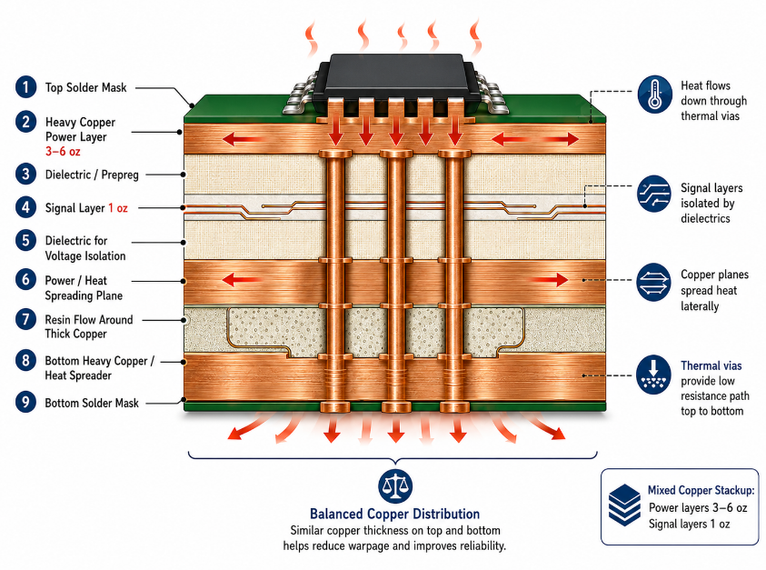
You may also like

What is a ceramic substrate PCB? PCB ceramic substrate

May 19th, 2026

What is a ceramic substrate for PCB?

Ceramic substrate for PCB refers to a specialized base material made from advanced ceramic compounds, designed to support and interconnect electronic components. Unlike conventional fiberglass-based laminates such as FR-4, ceramic substrates are engineered to deliver exceptional thermal stability, electrical insulation, and mechanical strength under demanding conditions.

In practical terms, a ceramic substrate circuit board is typically constructed using thick-film or thin-film processes. Conductive traces are printed or deposited directly onto the ceramic surface, forming highly reliable electrical pathways. These boards are often used in applications where heat management, reliability, and dimensional stability are critical—such as power electronics, RF modules, and high-frequency communication systems.

What is a ceramic substrate PCB? PCB ceramic substrate

From a design perspective, ceramic substrates offer a level of precision that is difficult to match with organic materials. Their low coefficient of thermal expansion (CTE) aligns closely with semiconductor devices, reducing mechanical stress during thermal cycling. This makes them particularly suitable for chip-on-board (COB) and direct die attachment configurations.

EBest Circuit (Best Technology), with its extensive experience in advanced PCB manufacturing, integrates ceramic substrate solutions into high-performance electronic assemblies. By combining precision fabrication techniques with strict quality control, We ensure that ceramic PCB substrates meet the rigorous demands of modern electronics.

What Materials Are Used for Ceramic Substrates PCB?

Ceramic substrate PCBs rely on a range of engineered ceramic materials, each selected based on performance requirements such as thermal conductivity, dielectric constant, and mechanical robustness. The most commonly used materials include:

  • Aluminum Oxide (Al₂O₃)
    Often referred to as alumina, this is the most widely used ceramic substrate material due to its cost-effectiveness and reliable performance. It provides good electrical insulation and moderate thermal conductivity, making it suitable for general-purpose applications.
  • Aluminum Nitride (AlN)
    Known for its exceptional thermal conductivity, aluminum nitride is ideal for high-power and heat-sensitive applications. It offers a thermal performance comparable to some metals while maintaining excellent electrical insulation.
  • Beryllium Oxide (BeO)
    This material delivers outstanding thermal conductivity but is less commonly used due to handling concerns. It is typically reserved for specialized, high-performance applications.
  • Silicon Nitride (Si₃N₄)
    Silicon nitride combines high mechanical strength with good thermal properties. It is particularly valued in applications requiring resistance to thermal shock and mechanical stress.

Each material brings a distinct set of advantages. For instance, alumina offers affordability and reliability, while aluminum nitride excels in thermal management.

What is a ceramic substrate PCB? PCB ceramic substrate

In advanced manufacturing environments like those at EBest Circuit, material selection is guided by both engineering analysis and real-world application experience. This ensures that each ceramic PCB substrate is optimized for its intended use.

What are the substrates for PCB?

Printed circuit boards can be built on a variety of substrate materials, each designed to meet different electrical, thermal, and mechanical requirements.

The most common PCB substrate types include:

  • FR-4 (Fiberglass Epoxy)
    The industry standard for general electronics, offering a balance of cost and performance.
  • Metal Core PCBs (MCPCB)
    Incorporate a metal base (usually aluminum) to improve heat dissipation.
  • Flexible Substrates (Polyimide)
    Used in applications requiring bending or dynamic movement.
  • Rogers and High-Frequency Laminates
    Designed for RF and microwave applications with controlled dielectric properties.
  • Ceramic Substrates
    Provide superior thermal conductivity, electrical insulation, and dimensional stability.

To better understand how ceramic substrates compare with traditional materials, the following table provides a clear overview:

PropertyFR-4Metal Core PCBCeramic Substrate PCB
Thermal ConductivityLowModerateHigh
Dielectric StabilityModerateModerateExcellent
Mechanical StrengthGoodGoodVery High
Operating TemperatureLimitedImprovedExtremely High
CostLowMediumHigher
ReliabilityStandardEnhancedPremium

Ceramic substrate PCBs distinguish themselves by delivering a unique combination of thermal and electrical performance. While they may involve higher upfront costs, their long-term reliability and efficiency often justify the investment.

How Does a Ceramic Substrate PCB Help with Heat Dissipation?

Heat management is one of the most compelling reasons to choose a ceramic substrate PCB. As electronic devices become more compact and powerful, efficient heat dissipation is no longer optional—it is essential for performance and longevity.

Ceramic materials inherently possess high thermal conductivity, allowing heat to spread rapidly across the substrate. This prevents localized hotspots, which can degrade components and reduce system reliability.

Several mechanisms contribute to the superior thermal performance of ceramic PCB substrates:

  • Direct Heat Conduction
    Heat generated by components is transferred directly into the ceramic substrate and distributed evenly.
  • Low Thermal Resistance
    Ceramic materials minimize resistance to heat flow, enabling efficient thermal transfer.
  • Stable Thermal Expansion
    Matching CTE between the substrate and components reduces stress and improves heat cycling performance.
  • Integration with Heat Sinks
    Ceramic substrates can be easily paired with external cooling solutions for enhanced thermal management.

Compared to traditional PCBs, ceramic substrates eliminate the need for additional thermal management layers or complex cooling structures. This not only simplifies design but also reduces overall system weight and footprint.

EBest Circuit leverages these advantages by offering precision-engineered ceramic PCB solutions tailored for high-power applications. Their manufacturing expertise ensures consistent thermal performance across production batches.

What features does COB ceramic substrate PCB possess?

COB (Chip-On-Board) ceramic substrate PCBs represent a highly integrated approach to electronic assembly. In this configuration, semiconductor chips are mounted directly onto the ceramic substrate, eliminating the need for traditional packaging.

What is a ceramic substrate PCB? PCB ceramic substrate

This design approach offers several distinctive features:

  • Compact Integration
    Direct chip attachment reduces size and improves signal integrity.
  • Enhanced Thermal Pathways
    Heat is transferred directly from the chip to the ceramic substrate.
  • Improved Electrical Performance
    Shorter interconnections minimize signal loss and latency.
  • High Reliability
    Fewer interconnect points reduce the risk of failure.
  • Precision Alignment
    Ceramic substrates provide a stable platform for accurate chip placement.

COB ceramic substrate PCBs are widely used in LED modules, sensors, and high-frequency devices. Their ability to combine compactness with performance makes them a preferred choice for advanced electronic systems.

At EBest Circuit, COB ceramic substrate solutions are developed with a focus on reliability and manufacturability. Their process control ensures consistent bonding quality and optimal performance.

What are ceramic PCBs used for?

Ceramic PCBs are deployed across a wide range of industries where performance and reliability are critical. Their unique properties make them indispensable in applications that demand high thermal efficiency and electrical precision.

Common applications include:

  • Power Electronics
    Used in inverters, converters, and power modules.
  • LED Lighting Systems
    Provide efficient heat dissipation for high-brightness LEDs.
  • Automotive Electronics
    Suitable for harsh environments and high-temperature conditions.
  • Telecommunications
    Ideal for RF and microwave circuits.
  • Medical Devices
    Ensure reliability in critical healthcare equipment.
  • Aerospace and Defense
    Deliver performance under extreme conditions.

These applications highlight the versatility of ceramic substrate PCBs. Whether in consumer electronics or mission-critical systems, they offer a dependable foundation for advanced circuitry.

What Are the Benefits of Ceramic Substrate PCBs?

Ceramic substrate PCBs deliver a compelling set of advantages that make them a preferred choice for high-performance applications. Their benefits extend beyond basic functionality, offering long-term value and reliability.

Key benefits include:

  • Exceptional Thermal Management
    Efficient heat dissipation enhances component lifespan.
  • High Electrical Insulation
    Prevents leakage and ensures stable operation.
  • Dimensional Stability
    Maintains structural integrity under temperature variations.
  • Chemical Resistance
    Resists corrosion and environmental degradation.
  • High-Frequency Performance
    Supports fast signal transmission with minimal loss.
  • Long Service Life
    Reduces maintenance and replacement costs.

These advantages translate into improved system performance and reduced operational risks. For engineers and designers, ceramic PCBs provide a reliable platform for innovation.

EBest Circuit integrates these strengths into their manufacturing processes, delivering ceramic PCB substrates that meet stringent industry standards. Our commitment to quality ensures consistent performance across applications.

What is a major disadvantage of ceramics?

While ceramic substrate PCBs offer numerous benefits, it is important to acknowledge their limitations to make informed design decisions.

The primary disadvantage is cost. Ceramic materials and manufacturing processes are generally more expensive than traditional PCB technologies. This can impact project budgets, especially for large-scale production.

Additionally, ceramics can be brittle, making them more susceptible to mechanical damage if not handled properly. However, modern engineering techniques have significantly improved their durability.

Despite these challenges, the advantages of ceramic substrates often outweigh the drawbacks in high-performance applications. When reliability and efficiency are priorities, ceramic PCBs remain a strong choice.

What is a ceramic substrate PCB? PCB ceramic substrate

FAQs About Ceramic Substrate PCB

1. Is ceramic substrate PCB better than FR-4?
It depends on the application. Ceramic PCBs outperform FR-4 in thermal and high-frequency scenarios, while FR-4 remains suitable for cost-sensitive designs.

2. Can ceramic PCBs be used in consumer electronics?
Yes, especially in devices requiring efficient heat management, such as LED lighting and power modules.

3. Are ceramic substrates environmentally stable?
They offer excellent resistance to moisture, chemicals, and temperature variations.

4. What industries benefit most from ceramic PCBs?
Automotive, aerospace, telecommunications, and medical industries are among the primary users.

5. How does EBest Circuit ensure quality?
Through strict process control, advanced manufacturing techniques, and adherence to international standards.

Summary:

Ceramic substrate PCBs represent a powerful evolution in circuit board technology. By replacing traditional organic materials with advanced ceramics, they deliver superior thermal performance, electrical stability, and long-term reliability. From power electronics to aerospace systems, their applications continue to expand as technology demands higher efficiency and durability.

For inquiries or technical support, feel free to reach out: sales@bestpcbs.com

You may also like

PTFE PCB Guide: Materials, Benefits, and Applications

May 19th, 2026

PTFE PCB plays an important role in RF, microwave, antenna, radar, and high-frequency communication products. Engineers choose PTFE-based circuit boards when they need low signal loss, stable impedance, and reliable high-frequency performance. Compared with standard FR4, PTFE materials offer better electrical stability at higher frequencies. However, material choice alone does not decide the final result. The stack-up, copper design, layout, drilling, plating, surface finish, and manufacturing control also matter. This guide explains what a PTFE PCB is, how PTFE laminate works, what layout factors need attention, and how to choose the right PTFE PCB manufacturer for your project.

PTFE PCB

What Is a PTFE PCB?

A PTFE PCB is a printed circuit board made with PTFE-based dielectric material. PTFE stands for polytetrafluoroethylene. It has low signal loss, low moisture absorption, strong chemical resistance, and stable electrical behavior.

Engineers often use PTFE boards in RF and microwave circuits. These circuits need better signal control than standard electronic boards. For example, antenna modules, radar boards, satellite communication products, RF amplifiers, and microwave devices often need PTFE materials.

A PTFE board may have one layer, two layers, or many layers. Some projects use pure PTFE laminate. Others combine PTFE with FR4 or other high-frequency materials. This hybrid structure can balance performance, cost, and strength.

PTFE behaves differently from FR4 during fabrication. It needs careful drilling, hole treatment, plating, lamination, and surface preparation. For this reason, a PTFE board requires more process control than a common FR4 board.

In simple terms, PTFE PCB is not just a board with a special material. It is a high-frequency circuit platform. Material, layout, stack-up, and manufacturing process must work together.

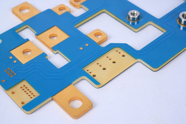
Why Do Engineers Use PTFE PCB Material in High-Frequency Circuits?

Engineers use PTFE PCB material because it helps high-frequency signals travel with less loss. At RF and microwave frequencies, the PCB trace acts like a transmission line. Small changes in material or trace shape can affect the signal.

PTFE material offers several key benefits:

  • Low dielectric constant
  • Low dissipation factor
  • Stable signal speed
  • Low moisture absorption
  • Good chemical resistance
  • Strong RF and microwave performance

These features help reduce signal loss. They also help keep impedance more stable. This matters in RF modules, antennas, filters, couplers, radar systems, and communication products.

FR4 works well for many standard electronic products. But it has higher loss at high frequencies. When a product needs cleaner signal transfer, PTFE becomes a better option.

Still, the material does not solve every problem. The layout must match the target impedance. The stack-up must match the design model. The copper thickness, dielectric thickness, via design, and surface finish also affect the final result.

That is why engineers should confirm the material and stack-up before production. Early review can save time and reduce design changes later.

PTFE PCB Laminate: Which Properties Matter Most?

A PTFE PCB laminate should match both electrical and production needs. Many buyers only check the dielectric constant. That is not enough. A good material choice needs a wider review.

PropertyWhy It Matters
Dielectric ConstantAffects impedance and signal speed
Dissipation FactorAffects signal loss
Laminate ThicknessHelps control impedance
Copper RoughnessAffects conductor loss at high frequency
Thermal ConductivityHelps manage heat
Dimensional StabilitySupports accurate layer alignment
Peel StrengthHelps copper stay bonded
Moisture AbsorptionHelps keep electrical values stable
Copper WeightAffects current, loss, and etching control

For RF circuits, dielectric constant and dissipation factor matter most. But copper roughness also plays a big role. At high frequencies, the signal travels near the copper surface. Rough copper can increase loss.

Laminate thickness also needs attention. If the thickness changes too much, impedance can shift. This may affect RF performance.

Before production, customers should confirm the laminate brand, thickness, copper weight, surface finish, and tolerance requirements. For multilayer boards, bonding material also matters.

A good PTFE PCB manufacturer should help review these details. The goal is simple: match the material with the real design and the real production process.

PTFE Teflon PCB vs FR4 PCB: What Is the Difference?

Many people use the term PTFE Teflon PCB when they talk about PTFE-based boards. Teflon is a well-known trade name. PTFE is the material name. In PCB projects, both terms often point to the same type of high-frequency board.

The main difference between PTFE and FR4 is electrical performance. FR4 works well for many common circuit boards. It offers good strength and a lower cost. PTFE offers better signal performance at high frequencies.

ItemPTFE Teflon PCBFR4 PCB
Main UseRF and microwave circuitsGeneral electronics
Signal LossLowerHigher at high frequency
Impedance StabilityBetter for RF designsGood for standard boards
CostHigherLower
Processing DifficultyHigherLower
Typical ProductsAntenna, radar, RF module, microwave boardControl board, power board, consumer electronics

You do not need PTFE for every board. If the product works at low speed or low frequency, FR4 may perform well. If the product works in RF or microwave bands, PTFE can give better results.

Some projects use both materials in one board. For example, the RF layer may use PTFE. Other layers may use FR4. This design can reduce cost while keeping RF performance where it matters.

The right choice depends on the frequency, signal loss target, cost target, board structure, and production volume.

How Does a High Frequency PCB with PTFE Improve Signal Performance?

A high frequency PCB with PTFE can improve signal performance by reducing loss and supporting stable impedance. In RF circuits, the board material becomes part of the circuit. The signal does not only travel through copper. It also interacts with the dielectric material around the trace.

PTFE helps in several ways.

First, it has a low dissipation factor. This reduces signal loss. It helps RF signals travel farther with less drop.

Second, it offers stable dielectric behavior. This helps engineers design accurate microstrip, stripline, and coplanar waveguide structures.

Third, it supports better phase stability. This matters in antennas, radar systems, and microwave communication products.

Fourth, it absorbs little moisture. This helps the board keep stable electrical behavior in changing environments.

However, PTFE does not work alone. The manufacturer must also control the board structure. Trace width, copper thickness, dielectric thickness, via position, solder mask, and plating thickness all affect the final result.

For example, a 50-ohm RF trace needs the right width and dielectric height. If the board thickness changes, impedance may shift. If copper plating becomes too thick, the trace shape may also change.

So, high-frequency PCB performance needs both good material and good manufacturing control.

How Should PTFE PCB Layout Be Designed for Stable High-Frequency Performance?

PTFE PCB layout should focus on signal path control, impedance stability, return path quality, and manufacturing feasibility. In many projects, the customer already has the circuit design. The PCB manufacturer mainly helps review the layout from a fabrication and DFM view.

Here are the key layout points.

Controlled Impedance

RF traces often need a clear impedance target, such as 50 ohms. The trace width, copper thickness, dielectric thickness, and ground plane all affect impedance. Before fabrication, the manufacturer should check whether the stack-up can meet the required value.

Short and Clean RF Paths

RF paths should stay as short and direct as possible. Sharp corners, sudden width changes, and long detours can affect signal quality. Smooth trace transitions help support stable performance.

Good Ground Reference

A stable ground plane helps the signal return path. RF layouts often need via stitching near signal paths, connectors, shielding areas, and ground edges. This helps reduce noise and improve RF behavior.

Proper Via Design

Vias affect high-frequency signals. Layout engineers should place RF vias carefully. Ground vias should support the return current path. Signal vias should avoid unnecessary length where possible.

Trace Width and Spacing

PTFE material needs careful process control. Very fine traces and tight spacing should match the manufacturer’s capability. A DFM review can confirm whether the design fits real production limits.

Copper Balance

Copper balance helps control board flatness and lamination behavior. This matters more in PTFE multilayer boards. Uneven copper can make production harder.

RF Connector Footprints

RF connectors need accurate pad size, ground pads, and solder mask clearance. A small footprint issue can affect both assembly and RF performance.

DFM Review Before Fabrication

A strong DFM review can check trace width, spacing, annular ring, via size, impedance stack-up, copper balance, panel design, and surface finish. This step helps turn layout data into a stable physical board.

For EBest Circuit, layout support mainly focuses on manufacturability, stack-up review, impedance feasibility, and production optimization. This helps customers improve the board before fabrication starts.

Rogers PTFE PCB: When Should You Choose Rogers-Based Materials?

A Rogers PTFE PCB can support RF and microwave products that need stable material quality. Rogers offers many high-frequency laminates. Some use PTFE-based systems, while others use different advanced resin systems.

Engineers often choose Rogers materials for:

  • RF modules
  • Microwave boards
  • Antenna circuits
  • Radar systems
  • Satellite communication products
  • Wireless infrastructure
  • High-speed test equipment

Rogers materials can offer low loss, stable dielectric values, and strong documentation. These features help engineers build more predictable RF products.

But Rogers is not the only option. Some projects may use Taconic, Isola, Panasonic, or other high-frequency materials. The best choice depends on the real application.

Before choosing a Rogers material, check these points:

  • Operating frequency
  • Target impedance
  • Board thickness
  • Copper weight
  • Loss requirement
  • Thermal demand
  • Layer count
  • Surface finish
  • Prototype or mass production plan

A good supplier should not simply suggest the most expensive material. Instead, the supplier should help match the material with performance, cost, and delivery needs.

For many projects, the best material is not the highest-grade material. It is the material that fits the design target and production plan.

Can PTFE Multilayer PCB Support Complex RF Designs?

Yes, PTFE multilayer PCB can support complex RF designs. It can combine RF signal layers, ground planes, power layers, control circuits, and shielding structures in one board.

This structure helps reduce board size. It also improves grounding and signal routing. Many RF modules, antenna systems, radar boards, and communication products use multilayer structures.

A typical PTFE multilayer board may include:

  • RF signal layers
  • Solid ground planes
  • Power layers
  • Digital control layers
  • Shielding areas
  • Via stitching
  • Hybrid PTFE and FR4 layers

Multilayer PTFE boards need strong process control. PTFE is softer than FR4. It also behaves differently during drilling and lamination. The manufacturer must control drilling, hole treatment, plating, bonding, and layer alignment carefully.

Hybrid stack-ups also need extra review. PTFE and FR4 do not expand in the same way under heat. The stack-up should account for this difference.

For RF products, the layer structure must also support impedance control. The distance between signal trace and reference plane must stay consistent. Copper thickness and dielectric thickness must match the design target.

Before production, customers should share the Gerber files, stack-up, impedance requirements, material choice, and special tolerance needs. This helps the manufacturer review the project clearly.

A PTFE multilayer PCB can work very well when design and production teams align early.

What Should Be Considered for RF Connector Assembly on PTFE PCB?

RF connectors play an important role in PTFE PCB performance. In many RF and microwave boards, the connector is not just a mechanical part. It is also the starting point of the signal path. If the connector footprint, soldering, grounding, or impedance transition is not well controlled, the board may lose part of its high-frequency advantage.

Connector Footprint Accuracy

The RF connector footprint should match the connector datasheet. Pad size, hole size, mounting position, solder mask opening, and ground pad layout all need careful review. For SMA, SMB, MMCX, or other coaxial connectors, even a small footprint error may affect assembly strength and RF performance.

50-Ohm Impedance Transition

Many RF connectors work with a 50-ohm transmission line. The transition from the connector pin to the PCB trace should stay smooth and controlled. Sudden trace width changes, long stubs, or poor pad geometry can create signal reflection. For PTFE PCB, the trace width should match the material thickness, copper thickness, and dielectric constant.

Ground Via Stitching

Good grounding helps the connector perform well. Ground vias should be placed close to the connector ground pads and around the RF launch area. This creates a shorter return path and helps reduce noise, radiation, and signal leakage.

Mechanical Stability

RF connectors often face repeated mating, cable pulling, and vibration. The PCB layout should provide enough copper area, mounting holes, and solder support. For heavier connectors, mechanical reinforcement may be needed to protect the solder joints and board edge.

Soldering Quality

PTFE PCB materials behave differently from FR4 during heating. The assembly process should control the soldering temperature, dwell time, and connector alignment. Clean solder joints help maintain both electrical performance and mechanical strength.

Board Edge and Connector Alignment

Many RF connectors mount at the board edge. The board outline, edge plating, connector position, and panel design should match the assembly requirement. Good alignment helps the cable connect smoothly and reduces mechanical stress.

Inspection After Assembly

After RF connector assembly, the board should be checked for solder quality, connector position, grounding, and mechanical strength. For high-frequency products, visual inspection, X-ray inspection, continuity testing, and RF-related testing may also be required based on the project.

In short, RF connector assembly on PTFE PCB requires close control of both layout and manufacturing details. A good PTFE PCB manufacturer should review the connector footprint, impedance transition, grounding method, soldering process, and inspection plan before production. This helps the final board keep stable RF performance after assembly.

PTFE PCB Manufacturing Capabilities at EBest Circuit (Best Technology)

PTFE PCB manufacturing needs stable material control, precise drilling, reliable plating, and strong impedance management. EBest Circuit (Best Technology) supports PTFE PCB fabrication, DFM review, PCBA assembly, component sourcing, testing, and turnkey electronics manufacturing for RF, microwave, antenna, radar, and communication applications.

CapabilityTechnical SpecificationBusiness Benefit
Material CoveragePTFE, Rogers, Taconic, Arlon, Nelco, and other RF laminatesMore choices for RF, microwave, antenna, and radar boards
Manufacturing Precision1–50 layers, 0.4–6.0 mm board thickness, 0.10 mm laser drilling, controlled impedance supportBetter signal stability and lower production risk
Quality CertificationsISO9001, ISO13485, IATF16949, AS9100D quality system supportSuitable for demanding industrial and regulated projects
Turnaround TimePrototype, small-batch, and volume production supportFaster project validation and smoother production planning
Global Sourcing & DeliveryPCB fabrication, component sourcing, PCBA assembly, testing, and deliveryLess supplier coordination and easier project management

Before production, EBest Circuit can review the material, stack-up, impedance target, trace width, via design, copper thickness, surface finish, and assembly needs. This helps customers reduce design-to-production risks and keep RF performance more stable.

For PTFE PCB projects, the goal is not only to manufacture the board. The goal is to keep the RF signal path stable from layout to final assembly. With DFM support, high-frequency PCB experience, and one-stop PCB/PCBA service, EBest Circuit helps customers move from prototype to reliable production.

Why Choose EBest Circuit (Best Technology) as Your PTFE PCB Manufacturer?

Choosing the right PTFE PCB manufacturer matters because PTFE boards need tighter process control than standard FR4 boards. The supplier should understand high-frequency materials, stack-up control, impedance, drilling, plating, and DFM review.

EBest Circuit (Best Technology) supports PCB fabrication, PCBA assembly, component sourcing, DFM review, testing, and turnkey electronics manufacturing. For PTFE and high-frequency PCB projects, the team can help review material choice, stack-up, impedance targets, layout feasibility, and production details.

Here are the main advantages.

High-Frequency PCB Experience

EBest Circuit works with high-frequency PCB materials for RF, microwave, antenna, communication, industrial control, automotive electronics, aerospace/UAV, and other electronic products.

DFM Review Before Production

The engineering team can review Gerber files, stack-up, trace width, spacing, via design, copper balance, impedance needs, and panel layout. This helps customers find possible issues before fabrication.

Controlled Impedance Support

Many PTFE boards need controlled impedance. EBest Circuit can help check the stack-up and production feasibility based on the target impedance.

PCB Fabrication and PCBA Assembly

Some customers need bare boards only. Others need complete assembly. EBest Circuit can support PCB fabrication, component sourcing, SMT assembly, through-hole assembly, testing, and box-build assembly.

Prototype to Batch Production

Many high-frequency projects start with samples. After testing, they move to small batch or volume production. EBest Circuit can support different stages with stable process control.

Quality and Traceability

EBest Circuit focuses on quality control, process records, and production traceability. This helps customers in industries that need stable documentation and reliable manufacturing support.

Clear Engineering Communication

High-frequency boards need clear communication. Small details can affect the final result. The team can discuss material, stack-up, tolerance, surface finish, assembly needs, and delivery plan with customers before production.

If you need PTFE PCB fabrication or turnkey assembly support, you can send Gerber files, stack-up, BOM, drawings, and technical requirements to sales@bestpcbs.com for review and quotation.

To summarize‌, a PTFE PCB is a strong choice for RF, microwave, antenna, radar, and high-frequency communication products. It helps reduce signal loss and supports stable electrical performance.

Still, the final result depends on more than material. The layout, stack-up, copper design, drilling, plating, surface finish, and assembly process all matter.

For high-frequency projects, an experienced PTFE PCB manufacturer can help make the process smoother. With early material review, layout checking, DFM support, and controlled fabrication, customers can move from prototype to production with more confidence.

FAQs About PTFE PCB

Q1: Is PTFE PCB only for RF circuits?
A1: PTFE PCB mainly serves RF, microwave, antenna, radar, and communication circuits. Some high-speed or low-loss products also use PTFE materials.

Q2: Is PTFE always better than FR4?
A2: No. PTFE works better for high-frequency and low-loss circuits. FR4 still works well for many standard electronic products. The best choice depends on frequency, cost, structure, and performance goals.

Q3: What files should I send for a PTFE PCB quote?
A3: You can send Gerber files, drill files, stack-up, board thickness, copper weight, surface finish, impedance needs, quantity, and special tolerance requirements. If you need assembly, also send the BOM and Pick-and-Place files.

Q4: Can PTFE PCB support SMT assembly?
A4: Yes. PTFE boards can support SMT assembly. The process should consider board thickness, material behavior, component type, soldering profile, and panel handling.

Q5: Which surface finish works well for PTFE PCB?
A5: ENIG often works well because it gives a flat and solderable surface. Other finishes may also fit some projects, depending on soldering, bonding, cost, and product needs.

Q6: Why does PTFE PCB cost more than FR4 PCB?
A6: PTFE materials cost more. The production process also needs tighter control. Drilling, hole treatment, plating, lamination, and impedance control all require more care.

Q7: Can PTFE work with FR4 in one board?
A7: Yes. Many designs use PTFE and FR4 together. This hybrid stack-up can balance RF performance, strength, board thickness, and cost.

Q8: How can I reduce risk before production?
A8: Confirm the material, stack-up, impedance target, copper thickness, via design, surface finish, and layout details early. A DFM review can help find issues before fabrication.

You may also like

Ceramic PCB Board – Aerospace AlN Ceramic PCB Board Manufacturer

May 18th, 2026

Ceramic PCB board is a high-performance circuit board built on a ceramic substrate instead of a conventional glass-fiber epoxy base. It is often selected when an electronic product needs excellent heat dissipation, dimensional stability, high insulation strength, and long-term reliability under demanding operating conditions. For aerospace electronics, power modules, RF devices, LED systems, medical equipment, and high-temperature industrial applications, ceramic circuit boards offer a strong foundation for designs where thermal and electrical performance matter from the first prototype to full production.

Ceramic PCB Board - Aerospace AlN Ceramic PCB Board Manufacturer

EBest Circuit (Best Technology) supports ceramic PCB fabrication, ceramic PCB prototype builds, ceramic substrate circuit board PCB PCBA projects, and engineering-driven manufacturing support for customers who need stable, production-ready solutions.

What Is a Ceramic PCB Board?

Ceramic PCB board is a printed circuit board that uses ceramic as the base substrate. The ceramic layer replaces the traditional FR4 laminate and provides stronger thermal conductivity, higher temperature resistance, and better electrical insulation. Conductive traces are formed on the ceramic surface through copper bonding, thick-film printing, thin-film metallization, or direct plated copper processes, depending on the application and performance target.

The main role of a ceramic PCB is to carry electronic circuits while also helping the product handle heat, stress, and electrical load more effectively. This makes it valuable for applications where a normal FR4 PCB may not provide enough thermal transfer or dimensional stability.

Ceramic circuit boards are often used in devices that must remain reliable for many years. These include aerospace power modules, RF amplifiers, laser systems, LED lighting modules, semiconductor test equipment, medical sensors, and industrial control products.

A ceramic PCB board may be supplied as a bare ceramic circuit board or as a fully assembled PCBA. A bare PCB board ceramic substrate includes the ceramic base, copper circuits, vias or pads if required, surface finish, and final inspection. A completed ceramic PCBA adds components, soldering, inspection, testing, and packaging. This full-process capability is useful when a customer wants one supplier to control fabrication, component sourcing, assembly, and quality verification.

How Is a Ceramic PCB Board Different from a Standard FR4 PCB?

Ceramic PCB board and an FR4 PCB both provide electrical interconnection, but they are designed for different performance levels. FR4 is a glass-reinforced epoxy laminate widely used in consumer electronics, control boards, communication devices, and general industrial products. It is affordable, easy to process, and suitable for many standard designs.

The biggest difference is the substrate. FR4 has relatively low thermal conductivity. It can work very well in many electronic products, but it does not move heat as quickly as ceramic. Ceramic materials such as aluminum nitride and alumina provide much stronger thermal paths.

Comparison ItemCeramic PCB BoardStandard FR4 PCB
Base MaterialAlumina, aluminum nitride, silicon nitride, or other ceramic substrateGlass fiber reinforced epoxy laminate
Thermal ConductivityHigh to very high, depending on ceramic materialLow, usually suitable for moderate heat loads
Temperature ResistanceExcellent for high-temperature environmentsGood for standard electronics, limited at higher temperatures
Electrical InsulationStrong insulation with good dielectric strengthGood insulation for common circuit designs
Dimensional StabilityVery stable under heatMore expansion under thermal stress
Typical ApplicationsAerospace, power electronics, RF, LED, medical, laser, semiconductor modulesConsumer electronics, general industrial boards, communication products
Cost LevelHigher because of material and process complexityLower and widely available
Prototype ConsiderationRequires careful design review and manufacturer experienceFaster and easier for common PCB factories
Assembly NeedsRequires controlled soldering and thermal process knowledgeMature and common SMT process flow

The choice is not about which material is always better. It is about whether the design needs the extra performance. For a simple control board with low heat, FR4 is often a smart choice. For a compact power module or aerospace AlN ceramic PCB board, ceramic can offer a stronger long-term solution.

What Are Ceramic Circuit Boards Used For?

Ceramic circuit boards are used in products where heat, power density, precision, and reliability must be controlled carefully. They are often found in industries that value stable performance over the full product life cycle.

In aerospace electronics, ceramic boards are used in power control modules, RF communication devices, sensor systems, radar-related circuits, and high-reliability control units. These products often work in environments with temperature changes, vibration, and strict weight limitations. A ceramic PCB can help engineers reduce thermal stress and improve circuit stability.

In power electronics, ceramic circuit boards are used for MOSFETs, IGBTs, power converters, motor drives, solid-state relays, and high-current modules. The ceramic substrate helps transfer heat from the power device to the heat spreader or housing. This supports smaller designs and more stable operating temperatures.

Ceramic PCB Board - Aerospace AlN Ceramic PCB Board Manufacturer

Common applications include:

  • Aerospace power modules, RF units, avionics sensors, and satellite-related electronic assemblies.
  • High-power LED modules, UV LED curing systems, automotive lighting, and industrial lighting engines.
  • RF and microwave circuits, including amplifiers, filters, antennas, and high-frequency ceramic substrate modules.
  • Medical electronics such as imaging equipment, sensor modules, laser systems, and diagnostic devices.
  • Semiconductor equipment, probe cards, laser diode carriers, and precision measurement instruments.
  • New energy products, charging modules, power conversion units, and thermal management assemblies.

Ceramic PCB boards are also widely used in high-end lighting. For example, LED chips generate concentrated heat. If that heat stays near the junction, brightness and life span can be affected. In RF applications, ceramic materials offer stable dielectric behavior. This is useful for circuits where signal loss, impedance control, and frequency stability are important.

What Ceramic PCB Materials Are Commonly Used?

The most common ceramic PCB materials include alumina, aluminum nitride, silicon nitride, and sometimes beryllium oxide in special legacy or niche applications. For modern commercial and industrial projects, alumina and aluminum nitride are the most widely used because they offer a practical balance of performance, manufacturability, availability, and cost.

Alumina ceramic, often written as Al₂O₃, is the most familiar option. It offers good insulation, good mechanical strength, stable performance, and a cost level that is more accessible than aluminum nitride. Common purities include 96% alumina and 99% alumina.

Aluminum nitride, written as AlN, is used when much higher thermal conductivity is required. Some buyers may search for an “aluminum nitride AIN ceramic PCB board,” although the correct chemical abbreviation is AlN. This material is especially attractive for aerospace, high-power LED, RF, laser, and power semiconductor applications. It offers excellent heat transfer while maintaining electrical insulation.

Ceramic PCB Board - Aerospace AlN Ceramic PCB Board Manufacturer

Silicon nitride is known for strong mechanical toughness and thermal shock resistance. It can be useful in applications where the board may face mechanical stress, impact risk, or repeated heating and cooling.

A simple way to view the material choices is this:

Ceramic PCB MaterialMain StrengthTypical Use CaseCost Tendency
96% AluminaGood insulation, stable processing, balanced costLED modules, sensors, industrial electronics, general ceramic PCB prototypeModerate
99% AluminaBetter purity, stronger electrical performancePrecision circuits, medical modules, high-reliability electronicsModerate to higher
Aluminum NitrideExcellent thermal conductivityAerospace, power modules, RF, laser diodes, high-power LEDHigher
Silicon NitrideHigh toughness and thermal shock resistanceHarsh mechanical or thermal environmentsHigher
Beryllium OxideVery high thermal performance but special handling concernsLimited specialized applicationsSpecial-case material

When selecting ceramic PCB materials, engineers should not only compare thermal conductivity values. They should also review copper bonding method, via structure, surface finish, operating voltage, component type, board size, tolerance, and assembly process.

What Is an Aluminum Nitride AlN Ceramic PCB Board?

An aluminum nitride AlN ceramic PCB board is a circuit board made with an AlN ceramic substrate. It is selected mainly for its excellent thermal conductivity and strong electrical insulation. For products that generate concentrated heat, AlN can help transfer heat away from components while still keeping the circuit electrically isolated.

AlN ceramic PCB boards are often used in aerospace electronics, laser diode modules, RF power amplifiers, high-brightness LED systems, power semiconductor packages, and new energy modules. In these products, heat is not just a side issue. It is one of the main factors that shapes the product’s service life, efficiency, and safety margin.

Aerospace applications are a strong fit for AlN because engineers often need compact and lightweight solutions. They also need materials that can perform through temperature changes and long operating cycles. An aerospace AlN ceramic PCB board can support this goal by combining thermal efficiency with a stable ceramic platform.

However, AlN projects require careful manufacturing control. The material is harder and more brittle than organic laminates, so drilling, cutting, metallization, and handling must be done with suitable process knowledge. Copper adhesion, surface flatness, laser processing, and final inspection are also important.

EBest Circuit supports aluminum nitride ceramic PCB manufacturing for customers who need high thermal performance, stable process control, and engineering communication during the design-to-production stage. For aerospace or other high-reliability projects, early DFM review is especially useful because it can help refine copper layout, board thickness, surface finish, and assembly method before production begins.

When Should You Choose Alumina Ceramic PCB Materials?

Alumina ceramic PCB materials are a strong choice when the design needs better thermal performance than FR4, good electrical insulation, stable mechanical properties, and a more economical ceramic option than AlN. Alumina is widely used because it offers a practical balance between performance and cost.

You may choose alumina when the heat load is moderate to high but does not require the premium thermal performance of aluminum nitride. It is common in LED modules, sensor boards, power control circuits, thick-film ceramic circuits, medical devices, and industrial electronics.

Alumina is available in different purity levels. A 96% alumina ceramic substrate is popular because it is cost-effective and reliable for many applications. A 99% alumina substrate can offer better purity and performance for more demanding circuits.

Before choosing alumina, engineers should review several points:

  • Thermal requirement: Alumina is better than FR4, but AlN is stronger for very high heat transfer.
  • Circuit density: Fine traces may require a more precise metallization process.
  • Operating environment: Alumina performs well in high-temperature and stable insulation applications.
  • Cost target: Alumina often supports a more controlled ceramic board price than premium ceramic materials.
  • Assembly plan: Component size, soldering profile, and thermal mass should be reviewed early.

Alumina is also suitable for ceramic PCB prototype projects. When a customer wants to validate a ceramic design before mass production, alumina can provide a dependable starting point. It allows engineers to test thermal behavior, mechanical fit, surface finish, solderability, and electrical function without immediately moving to a more expensive material.

What Is a Bare PCB Board Ceramic Substrate?

A bare PCB board ceramic substrate is a ceramic circuit board before electronic components are assembled. It includes the ceramic base, conductive circuits, pads, vias if required, and surface finish.

For a ceramic PCB, the bare board stage is especially important. The substrate material, copper bonding, circuit pattern accuracy, hole quality, surface finish, and inspection process all affect the final PCBA. If the bare ceramic circuit board is not controlled properly, assembly yield and long-term reliability can be affected.

A bare ceramic board may use several circuit-forming technologies. Thick-film ceramic circuits are made by printing conductive paste and firing it at high temperature. Thin-film ceramic circuits use vacuum deposition and etching to create fine patterns. DBC, or direct bonded copper, bonds copper directly to ceramic at high temperature and is often used for power modules. DPC, or direct plated copper, can create more precise copper features and plated vias for advanced designs.

The surface finish is also important. Common options may include ENIG, silver, gold plating, nickel plating, or other finishes depending on soldering and bonding needs. For wire bonding, the finish must support reliable bond strength.

A bare PCB board ceramic product is often ordered by customers who handle assembly internally or send it to another EMS provider. However, many customers now prefer one-stop support because ceramic boards require closer coordination between fabrication and assembly.

EBest Circuit provides bare ceramic PCB board manufacturing as well as assembled ceramic PCBA service. This helps customers move from ceramic substrate design to finished electronic module with better process continuity.

How Is a PCB Ceramic Circuit Board Manufactured?

A PCB ceramic circuit board is manufactured through a controlled process that depends on the ceramic material, copper structure, circuit density, and end application.

The manufacturing journey usually begins with engineering review. The manufacturer checks the Gerber files, stackup, substrate material, copper thickness, hole design, surface finish, tolerances, and assembly requirements. After the review, the ceramic substrate is prepared. The substrate must meet thickness, flatness, and surface quality requirements. Depending on the process, the circuit layer may be created by printing conductive paste, bonding copper foil, sputtering metal layers, or plating copper.

Typical manufacturing steps include:

  • Material selection and DFM review based on thermal, electrical, and mechanical requirements.
  • Ceramic substrate preparation, cleaning, thickness control, and surface inspection.
  • Circuit formation through thick film, thin film, DBC, DPC, or another suitable process.
  • Hole processing, laser drilling, mechanical drilling, or via formation where required.
  • Copper patterning, etching, plating, or metallization control according to the design.
  • Surface finish application for soldering, wire bonding, or corrosion protection.
  • Electrical test, dimensional inspection, visual inspection, and packaging.

For DBC ceramic boards, copper is bonded to ceramic at high temperature. This method is excellent for power electronics because it supports thicker copper and strong thermal paths. For DPC ceramic boards, copper is built through plating, which can support finer features and plated vias. For thin-film ceramic boards, the process can create very precise patterns for RF, sensor, and high-frequency applications.

Ceramic PCB Board - Aerospace AlN Ceramic PCB Board Manufacturer

Can Ceramic PCB Boards Support PCBA Assembly?

Yes, ceramic PCB boards can support PCBA assembly, and many ceramic projects are built as complete assembled modules. In fact, ceramic substrates are often selected because they provide a better base for high-power components, LEDs, RF devices, sensors, and semiconductor packages.

Ceramic PCBA assembly requires more process attention than standard FR4 assembly. The board has different thermal behavior, higher rigidity, and lower flexibility. Soldering profiles must be controlled carefully because ceramic substrates conduct and absorb heat differently. Components with large thermal pads, power packages, or bottom terminations may need special stencil design and solder paste control.

SMT assembly on ceramic boards can include LEDs, ICs, resistors, capacitors, MOSFETs, sensors, connectors, and custom components. Some designs may also use wire bonding, die attachment, or hybrid assembly methods.

For ceramic substrate circuit board PCB PCBA projects, the best results usually come from close cooperation between the board manufacturer and assembly team. Pad design, surface finish, solder paste type, reflow curve, component thermal path, and inspection method should be considered together. A ceramic PCB can also support testing after assembly. Depending on the product, testing may include visual inspection, AOI, X-ray inspection, electrical testing, functional testing, thermal testing, or reliability screening..

EBest Circuit (Best Technology) offers one-stop PCB and PCBA manufacturing support, including ceramic PCB fabrication, component sourcing, SMT assembly, testing, and engineering communication. For customers who need both bare board ceramic substrates and assembled modules, this integrated support can reduce coordination gaps and help the project move faster from prototype to production.

How Do You Choose a Reliable Ceramics PCB Board Manufacturer?

Choosing a reliable ceramics PCB board manufacturer requires more than comparing unit price. Ceramic boards involve special materials, precision processing, thermal design, and assembly knowledge. A low quote may look attractive at the beginning, but the real value comes from stable quality, clear communication, process capability, and the ability to support your product through prototype and production.

First, review the manufacturer’s ceramic material experience. A capable supplier should understand alumina, aluminum nitride, and other ceramic PCB materials. They should be able to explain which material fits your application and why.

Second, check the process capability. Different ceramic circuit boards may require DBC, DPC, thick-film, thin-film, laser drilling, copper plating, precision cutting, or special surface finishes.

Third, evaluate engineering support. Ceramic PCB designs often benefit from DFM review before production. A good engineering team can help check pad design, thermal path, board thickness, surface finish, panelization, and manufacturability.

Fourth, confirm quality control and traceability. For aerospace, medical, industrial, and power electronics, documentation matters. Inspection records, material control, electrical testing, dimensional reports, and production traceability can give customers more confidence.

EBest Circuit (Best Technology) is positioned as an engineering-driven PCB and PCBA manufacturing partner. The company supports ceramic PCB board fabrication, ceramic circuit boards, ceramic PCB prototype builds, PCB ceramic circuit board production, component sourcing, PCBA assembly, and testing. For customers working on aerospace AlN ceramic PCB boards, LED thermal modules, power electronics, medical devices, or industrial control products, EBest provides practical support from design review to production delivery.

For ceramic PCB board manufacturing, ceramic PCB prototype support, or ceramic PCB PCBA assembly, you can contact EBest Circuit (Best Technology) at sales@bestpcbs.com

You may also like