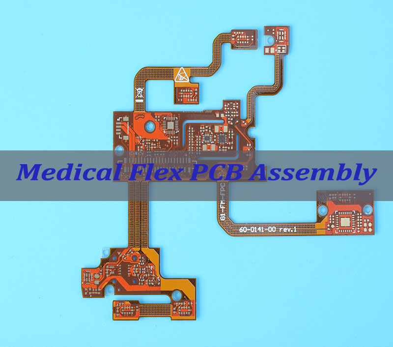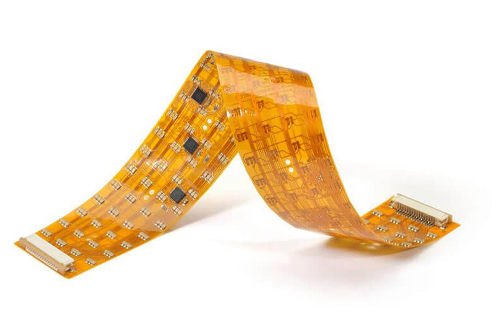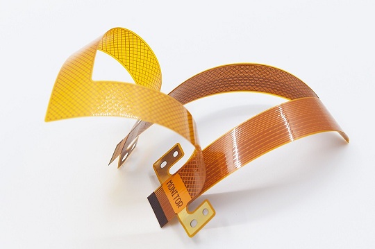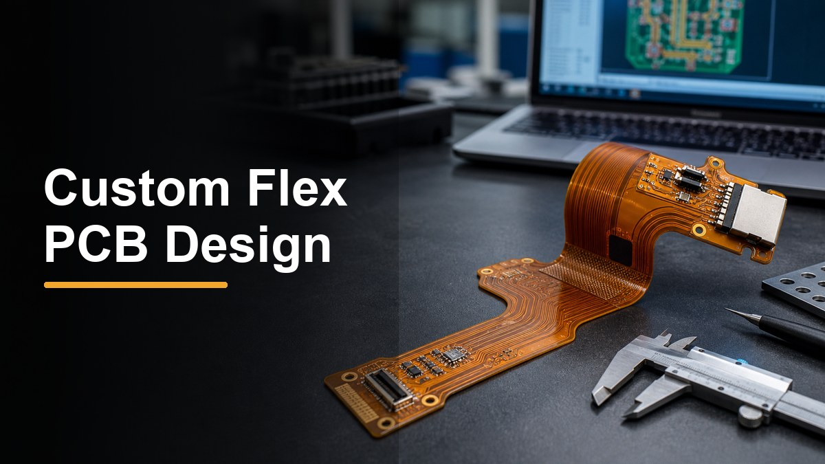
Custom flex PCB design is the process of defining a flexible printed circuit so it can bend, fold, connect and survive production without cracked copper, torn coverlay or weak connector areas. The core checks are bend radius, stackup, copper type, coverlay openings, stiffener support, component placement, panelization and test requirements.
This guide is written for engineers and buyers who already know they need a flex circuit, but want a cleaner file package before requesting a quote. It avoids generic FPC definitions and focuses on the details that usually decide whether the design is manufacturable.
What Makes a Custom Flex PCB Different from a Rigid PCB?
A custom flex PCB must be designed around movement, installation space and material stress, while a rigid PCB mainly stays flat after assembly.
FR4 boards can tolerate many layout habits that do not work on polyimide flex circuits. In a flex area, trace direction, copper grain, bend location, adhesive system and coverlay opening all affect reliability. If the layout treats the flex section like a thin rigid board, the first risk is usually copper fatigue near connectors, vias or the bend transition.
| Design point | Rigid PCB habit | Flex PCB design check |
| Bending | Usually not considered after installation | Define static or dynamic bend, bend direction and minimum bend radius |
| Material | FR4 laminate is common | Polyimide, adhesiveless laminate, rolled annealed copper or electrodeposited copper may be reviewed |
| Solder mask | Liquid solder mask is common | Coverlay openings and adhesive squeeze-out need review |
| Support | Board thickness gives support | Stiffeners may be needed under connectors, components or fingers |
| Files | Gerber and drill data may be enough for simple jobs | Mechanical drawing, bend notes, stackup and stiffener details should be included |
For rigid sections or combined constructions, compare the flex design with the site’s rigid flex circuit capability so the board type is clear before quoting.
Start with the Bend Radius and Bend Type
Bend radius should be defined before routing because it controls trace stress, layer count, copper choice and the safe location of vias or components.
A static bend usually happens during installation and then stays in place. A dynamic bend moves repeatedly during use, such as in a hinge, printer path, camera module or sliding mechanism. Dynamic flex areas normally need more conservative routing, fewer copper layers in the bend zone, smoother trace transitions and a larger bend radius than one-time installation bends.
Use IPC-2223 as a design reference point, but do not treat a single bend-radius number as universal. The practical limit depends on total flex thickness, number of copper layers, copper type, bend angle, coverlay, adhesive, temperature and expected cycles. For a deeper standards-oriented explanation, see the related IPC-2223 flex PCB design and bend radius guide.
| Bend situation | Main design risk | What to specify |
| One-time installation bend | Assembly damage during folding | Bend line, bend direction, minimum radius and keep-out areas |
| Repeated dynamic bend | Copper fatigue and coverlay cracking | Cycle expectation, bend radius, copper type and test method |
| Bend near connector | Pad lifting or cracked solder joints | Connector support, stiffener size and distance from bend zone |
| Tight enclosure routing | Over-bending during final assembly | 3D mechanical constraint, fixture path and installation notes |
Choose the Stackup Around Movement, Not Only Layer Count
A flex PCB stackup should reduce bending stress first, then satisfy signal, shielding, impedance and assembly needs.
Single-layer and double-sided flex circuits are easier to bend than multilayer flex circuits. Adding layers can help routing density, shielding or impedance, but it also increases thickness and bending stress. If the product needs a very tight bend, routing more signals through a wider flex tail may be safer than forcing too many layers into a narrow moving section.
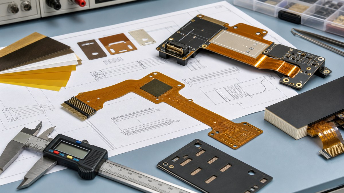
Material choice also matters. The flexible PCB materials used for the base film, adhesive system, coverlay and copper foil can change flexibility, dimensional stability and soldering behavior. For a moving product, ask the manufacturer to review whether rolled annealed copper, adhesiveless laminate or a thinner construction is more suitable than a default build.
Keep Vias, Pads and Components Away from the Bend Area
The safest flex bend area is usually a clean copper-trace zone without vias, plated holes, solder joints or heavy components.
Vias and plated holes create local stiffness changes. Components add mass and solder-joint stress. Sharp trace corners, sudden width changes and dense copper transitions can become fatigue points when the flex circuit bends. For that reason, the bend area should be treated as a controlled mechanical zone rather than leftover routing space.
- Route traces perpendicular to the bend line when possible.
- Use curved or gradual trace transitions instead of sharp 90-degree corners.
- Avoid placing vias, test pads or solder joints directly in the bend area.
- Balance copper distribution so one side of the flex area is not much stiffer than the other.
- Define keep-out zones for screws, housing ribs, adhesive and moving parts.
Use Stiffeners Where Connectors and Components Need Support
Stiffeners do not make a flex PCB more flexible; they protect selected areas that must behave like a rigid mounting surface.
Common stiffener materials include FR4, polyimide, stainless steel and aluminum, depending on thickness, heat exposure, grounding needs and assembly method. Stiffeners are often used under ZIF connector tails, soldered connectors, keypads, fingers, SMT component zones and assembly handling areas. The key is to stop the stiffener edge from becoming a stress concentration at the start of the bend.
| Stiffener location | Why it is used | RFQ detail to provide |
| Connector tail | Controls insertion thickness and connector support | Connector model, final thickness and exposed finger length |
| SMT component zone | Supports solder joints during handling and use | Component height, assembly side and reflow requirement |
| Mounting or screw area | Prevents tearing around holes | Hole size, tolerance, adhesive area and housing contact |
| Transition from rigid to flex | Controls stress near the flex exit | Stiffener edge, bend line distance and radius expectation |
Define Coverlay, Openings and Surface Finish Early
Coverlay design affects solderability, insulation, flexibility and how much copper remains protected during bending.
Unlike rigid PCB solder mask, flex PCB coverlay is usually a polyimide film with adhesive. Openings around pads must be large enough for manufacturing tolerance and soldering, but not so large that nearby copper is left unprotected in a bend-prone area. If the flex tail uses gold fingers, specify finger thickness, final thickness and insertion direction. For soldered pads, confirm whether ENIG, OSP, immersion tin or another surface finish fits the assembly plan.
If the project uses etched flex circuits with unusual shapes, copper details or connector geometry, the related custom etched flex circuits article is a useful supporting reference.
Plan Assembly Before Fabrication Files Are Frozen
Flex PCB assembly should be reviewed before fabrication because stiffener, panelization and component placement can change how the board is built.
Some flex circuits are supplied bare. Others need SMT assembly, connector soldering, metal dome placement, adhesive backing or final box build. If assembly is part of the project, discuss handling tabs, carrier panels, fiducials, component side, reflow exposure and inspection access before freezing the Gerber package. For assembled flex circuits, Best Technology’s quick-quote flex PCB assembly page is a relevant service page to review.
The following FPC manufacturing process video is relevant because it shows actual flexible circuit production context. The article remains complete without the video, but the visual process can help buyers understand why stackup, coverlay and bend details matter.
Prepare an RFQ File Package That a Manufacturer Can Review
A strong RFQ package should let the manufacturer review electrical design, mechanical bending and assembly risk without guessing.
For simple rigid PCBs, Gerber, drill and quantity may start a quote. For a flex circuit, missing mechanical details often cause delays or incorrect assumptions. The drawing should show board outline, bend line, bend direction, bend angle, minimum radius, stiffener size, final thickness, connector area and any adhesive or shielding requirement.
- Gerber or ODB++ fabrication files.
- Drill file and slot requirements.
- Stackup target, material notes and copper weight.
- Mechanical drawing with bend lines, stiffeners, tolerances and final thickness.
- BOM, centroid file and assembly drawing if components are included.
- Surface finish, coverlay color, marking and adhesive backing notes.
- Test requirements, such as electrical test, continuity test or fixture needs.
- Quantity, delivery target and whether the design is prototype or production.
Check Testing and Inspection Requirements Before Production
Testing should match how the flex circuit will fail in real use, not only whether nets are connected at the factory.
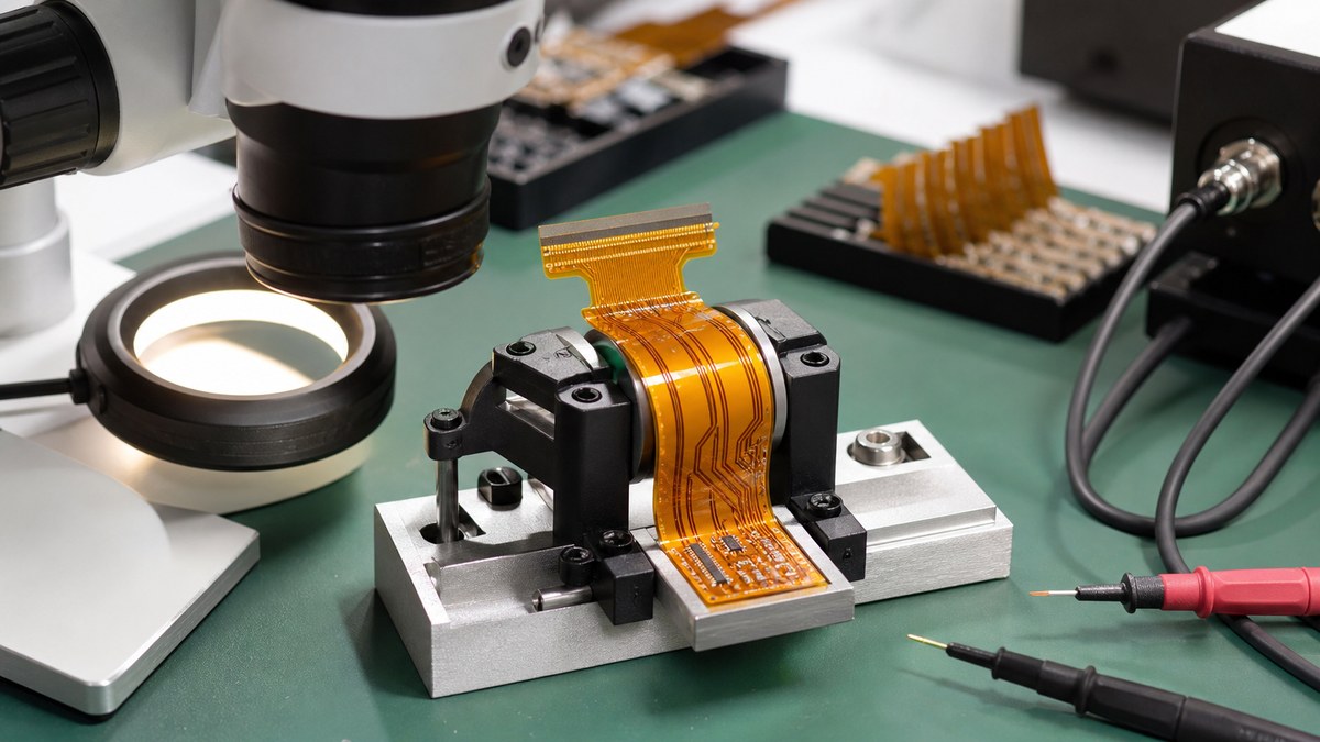
Electrical test can catch opens and shorts, but it may not prove the flex tail will survive the product’s bend path. Visual inspection, dimensional checks, continuity testing after forming, connector fit and sample bending review may be needed for higher-risk designs. For projects that need inspection capability context, the site’s PCB test equipment page gives useful background on available quality-control tools.
Common Flex PCB Design Mistakes
Most flex PCB problems come from treating the board as a flat electrical layout after the mechanical constraints have already been decided.
| Mistake | Likely result | Better action |
| No bend radius shown on drawing | Manufacturer guesses the mechanical limit | Add bend line, direction, radius and bend type |
| Vias placed in bend area | Cracking, intermittent opens or plating stress | Move vias into supported zones |
| Connector without stiffener | Poor insertion support or solder-joint stress | Specify stiffener material and final thickness |
| Dense copper in one side of bend | Uneven stiffness and local stress | Balance copper or adjust routing |
| Assembly not discussed until after fabrication | Panelization or handling problems | Review assembly method before release |
How to Choose a Custom Flex PCB Supplier
A suitable supplier should review mechanical and manufacturing risk, not only quote from Gerber files.
Ask whether the supplier can review bend radius, stackup, coverlay, stiffener, panelization and assembly together. A low quote is not useful if the design cracks during installation or needs a board respin because the flex exit was not checked. For early projects, a manufacturer that can support prototypes, engineering feedback and assembly review is usually more useful than a quote-only channel.
- Can you review the bend radius against the proposed stackup?
- Which copper type and laminate system do you recommend for static or dynamic bending?
- Where should stiffeners be added, and what final thickness is realistic?
- Do you need a 3D model or mechanical drawing to confirm the bend path?
- Can you build both bare flex PCB and assembled flex PCB if the project moves to PCBA?
- What inspection or sample validation should be done before mass production?
FAQ About Flex PCB Design
What is a custom flex PCB?
It is a flexible printed circuit made to a specific outline, bend path, connector layout, stackup and application requirement. It is usually built on polyimide film and may include coverlay, stiffeners, adhesive backing, shielding or assembled components.
What files are needed for a flex PCB quote?
Send Gerber or ODB++ files, drill data, stackup notes, quantity and a mechanical drawing. For flex circuits, the drawing should include bend line, bend direction, minimum radius, stiffener details, final thickness and connector information. Add BOM and centroid data if assembly is needed.
Is bend radius the same for every flex PCB?
No. Bend radius depends on flex thickness, copper layers, copper type, adhesive system, coverlay, bend angle and whether the circuit bends once or moves repeatedly. Use IPC-2223 as a reference, then confirm the actual stackup with the manufacturer.
Should components be placed on a flex PCB?
Components can be placed on flex circuits, but they usually need a supported area, stiffener or controlled handling method. Avoid placing components in active bend zones. If the product needs many components, rigid-flex construction may be more reliable than a fully flexible board.
What is the difference between flex PCB and rigid-flex PCB?
A flex PCB is mainly flexible material, while a rigid-flex PCB combines rigid board sections and flexible interconnect sections in one construction. Rigid-flex is useful when components need rigid support but the product still needs folding or three-dimensional packaging.
Why are stiffeners used in flexible PCBs?
Stiffeners support selected areas such as connectors, SMT zones, fingers or mounting holes. They help control insertion thickness, solder-joint stress and handling damage. They should be placed carefully so the stiffener edge does not create a new stress point.
Can a custom flex PCB be assembled with components?
Yes. Many custom flex PCBs can be assembled with SMT parts, connectors, domes or adhesive-backed components. The assembly plan should be reviewed before fabrication so panelization, stiffener location, fiducials, reflow exposure and inspection access are correct.
What increases flex PCB cost?
Cost can increase with tighter bend requirements, multilayer flex stackups, fine traces, special copper, stiffeners, adhesive backing, impedance control, dynamic bending validation, low-volume setup and assembly complexity. A complete drawing helps the supplier quote these factors accurately.
How can buyers reduce flex PCB production risk?
Provide the mechanical drawing early, confirm bend radius, keep vias out of bend areas, define stiffeners, review material choice and validate a prototype before volume production. Do not wait until enclosure assembly to discover that the bend path is too tight.
Is a video required in every flex PCB article or page?
No. A video is useful only when it directly supports the topic. For a custom flex PCB design article, a manufacturing process video can help explain why material, coverlay and bend details matter, but the written RFQ checklist should still stand alone.
Final Custom Flex PCB RFQ Checklist
A flex circuit is ready for quotation when the supplier can see both the electrical circuit and the mechanical bending requirement.
Before sending the RFQ, check that the package includes Gerber or ODB++ files, drill data, stackup, material notes, coverlay openings, bend radius, bend direction, stiffener drawing, final thickness, surface finish, assembly files if needed and test expectations. If any of those details are uncertain, ask for engineering review before production release.
If you are sourcing custom flex PCB, rigid-flex PCB or assembled flexible circuits for prototypes or production, send the design files, mechanical drawing and target application to our engineering team for a manufacturability review and quote at sales@bestpcbs.com.