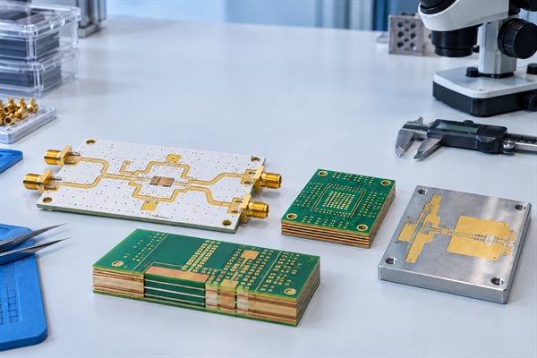
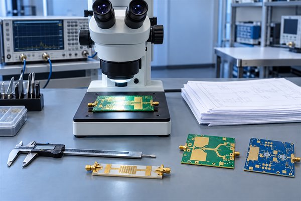
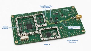
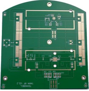
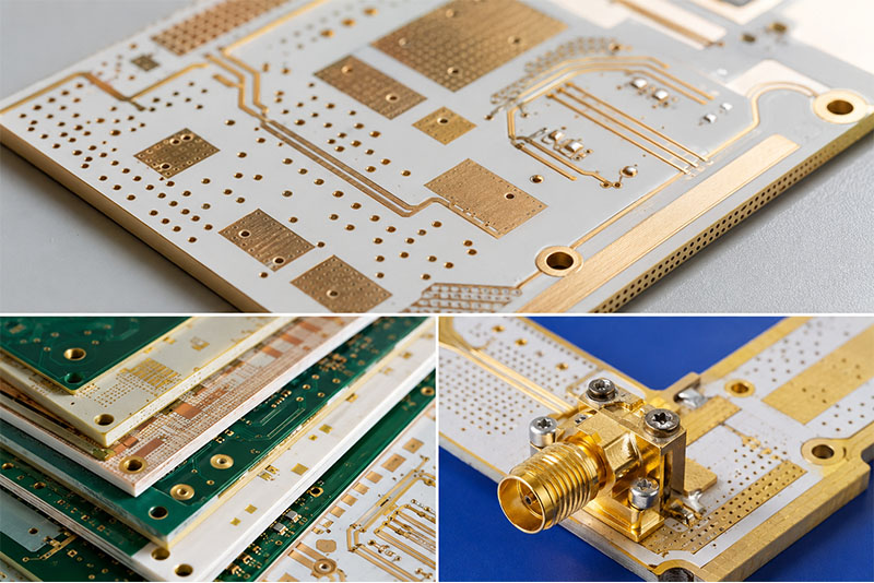
High-frequency PCB manufacturers in Europe cover PTFE multilayers, RF/FR-4 hybrid stackups, HDI, controlled impedance, 24–77 GHz radar PCBs, metal-backed boards, and RF testing. This guide compares seven manufacturers with documented European production and published high-frequency PCB capabilities.
Top 7 High-Frequency PCB Manufacturers in Europe
The seven manufacturers below differ mainly in RF material experience, layer structure, mmWave capability, HDI processing, production location, lead time, and target applications. The table provides a direct comparison of their published manufacturing strengths.
Manufacturer
Manufacturing Site
Process Capability
Lead Time
Strength
ACB
France
PTFE, microwave laminates, multilayer RF PCB
Quick-turn available; by quote
RF and microwave PCB specialization
Aspocomp
Oulu, Finland
PTFE, RF/FR-4 hybrid, HDI, microvias, via filling
3–20 days
RF + HDI integration
AT&S
Fehring, Austria
High-frequency PCB up to 10 layers, multilayer, HDI
By quote
Advanced multilayer capability and broad certifications
Eurocircuits
Europe
Rogers 4000 series, I-Tera, 2- and 4-layer RF PCB
5 days bare / 10 days assembled for eligible RF Pool orders
What High-Frequency PCB Capabilities Do European Manufacturers Offer?
European manufacturers cover both conventional microwave PCBs and more complex structures that combine RF materials, multilayer construction, HDI, fine conductor control, thermal management, and mmWave processing. The following capabilities are the most relevant when comparing factories.
Microvias, blind vias, buried vias, stacked and staggered vias
Controlled Impedance
Controlled-impedance transmission lines and verification
Fine-Line Etching
Published tolerances down to ±15 µm for selected processes
mmWave PCB
24 GHz and 77 GHz radar and sensor PCB production
Via Processing
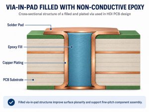
Via filling, copper-filled vias, via-in-pad
Special Structures
Metal-backed PCB, cavities, controlled-depth features
Assembly
SMT and RF PCB assembly
Testing
Electrical test, impedance verification, RF/microwave test
At higher frequencies, trace width, dielectric thickness, copper profile, registration, and material stability have greater influence on impedance and insertion loss. For hybrid RF/FR-4 multilayers, lamination and dimensional compensation also become critical process controls.
Which Certifications Matter When Choosing a High-Frequency PCB Manufacturer in Europe?
Certifications should be matched to the application, production site, and required quality system. They are particularly relevant for automotive, aerospace, medical, and other regulated electronics.
ISO 9001 — quality management system for general PCB manufacturing.
IATF 16949 — relevant to automotive radar, ADAS, vehicle sensing, and automotive communication electronics.
EN 9100 / AS9100 — used for aerospace and aviation electronics where traceability and process control requirements are higher.
ISO 13485 — relevant to PCB production for medical devices and medical electronics.
NADCAP — applies to qualified special processes in aerospace supply chains where required.
ISO 14001 — covers environmental management systems.
IPC-6018 — covers performance requirements for high-frequency and microwave printed boards.
Before supplier approval, verify the certificate holder, factory address, certification scope, and validity period against the site that will manufacture the PCB.
How Does Lead Time Differ Among European High-Frequency PCB Manufacturers?
High-frequency PCB lead time varies with RF material availability, PCB structure, lamination cycles, HDI processing, special mechanical features, testing, and assembly. Published quick-turn times normally apply only to designs that fit a defined process window.
Manufacturer
Lead Time
Scope
ACB
Quick-turn available
Project-specific RF build
Aspocomp
3–20 days
Oulu production
AT&S
By quote
Site and construction dependent
Eurocircuits
5 days bare / 10 days assembled
Eligible RF Pool orders
KSG
By quote
Material and PCB structure dependent
Schweizer Electronic
By quote
Project-specific RF production
Teledyne Labtech
From 5 days
Qualifying prototypes
Lead time usually increases with:
special-order RF laminates
high layer count
PTFE or mixed-dielectric lamination
sequential lamination
microvias and filled vias
cavities or controlled-depth routing
metal-backed structures
additional impedance or RF testing
PCB assembly
For supplier comparison, use the required delivery date, not fabrication days alone. Material procurement, inspection, assembly, freight, and customs can materially change the final schedule.
How Does European High-Frequency PCB Manufacturing Compare With Asian Manufacturing?
For most sourcing decisions, the practical comparison is quality control, lead time, cost, process capability, material availability, engineering support, and production capacity. These factors affect both prototype development and volume production.
Factor
European Manufacturing
Asian Manufacturing
Quality Control
Strong specialist RF factories and sector-specific quality systems
Established RF factories can support tight impedance, HDI, and high-reliability production
Lead Time
Shorter transport for European deliveries
Fast fabrication possible; international freight and customs add time
Cost
Higher labor and manufacturing overhead
Generally more competitive for medium- and high-volume production
Process Capability
Strong in specialty RF, radar, aerospace, and complex prototypes
Broad capability across RF, HDI, multilayer, hybrid, rigid-flex, and volume production
RF Materials
Strong specialist laminate experience
Broad material sourcing network and supplier base
Prototype Support
Strong regional quick-turn options
Competitive prototype fabrication with longer logistics to Europe
Volume Capacity
Some suppliers focus on specialty or lower-volume programs
Stronger large-volume manufacturing capacity
Engineering Support
Easier time-zone alignment for European programs
Depends on supplier engineering resources and response process
Production Origin
Suitable where European manufacture is required
Suitable where offshore manufacturing is accepted
Total Cost
Higher manufacturing cost but shorter regional logistics
Lower production cost; freight, customs, and inventory must be included
European production is more suitable when local origin, regional engineering access, specialist RF processing, or shorter European logistics are required. Asian production is often stronger when volume capacity and manufacturing cost are higher priorities.
How Should You Choose the Right High-Frequency PCB Manufacturer in Europe?
The supplier should be evaluated against the actual RF stackup and the processes that are hardest to control on the board. A useful qualification compares measurable manufacturing capability rather than general claims such as “RF PCB supported.”
Match the manufacturer to the operating frequency. A manufacturer experienced with a 2–6 GHz communication board is not automatically qualified for a 24 GHz or 77 GHz radar PCB. Check whether the factory has documented production experience near the required frequency range and with similar transmission-line structures.
Confirm the exact RF material system. Specify the complete laminate grade rather than writing only “Rogers PCB” or “PTFE PCB.” Verify the core, prepreg or bonding material, dielectric thickness, copper type, material availability, and approved alternatives.
Review the proposed stackup before releasing production files. For RF/FR-4 hybrid multilayers, confirm layer order, dielectric thickness, finished copper, impedance targets, lamination sequence, and material compatibility. Any stackup change can alter trace dimensions and impedance.
Check the processes that affect RF performance. The most relevant controls include etching tolerance, conductor width, copper profile, dielectric thickness, registration, lamination, controlled-depth machining, and surface finish. For mmWave designs, small dimensional changes can have a measurable electrical effect.
Verify HDI and via capability where required. For dense RF/digital boards, check microvia diameter, blind and buried vias, via-in-pad, copper filling, stacked or staggered vias, and sequential lamination. Confirm that these processes are qualified with the selected RF laminate rather than only standard FR-4.
Confirm impedance control and inspection methods. Define the required impedance and tolerance on the fabrication drawing. Ask whether verification includes impedance coupons, TDR results, microsections, dimensional inspection, or other project-specific records.
Check special RF and thermal structures. For high-power amplifiers, radar modules, antennas, or microwave systems, verify capability for metal-backed PCBs, cavities, thermal vias, copper-filled vias, controlled-depth routing, edge plating, or other required structures.
Match certifications to the final application. A standard industrial RF PCB may require ISO 9001, while automotive radar may require IATF 16949 and aerospace electronics may require EN 9100/AS9100 or additional process approvals. Confirm that the certificate covers the actual production site.
Compare lead time using the same starting point. Ask each manufacturer to quote from engineering approval and material availability through fabrication, inspection, assembly, and dispatch. This avoids comparing a five-day fabrication cycle with another supplier's complete delivery schedule.
Check prototype and production capacity separately. A supplier may be excellent at prototypes but have limited volume capacity. Confirm prototype quantity, monthly production demand, panel requirements, expected ramp-up, and whether the same factory and process will be used after qualification.
Confirm the manufacturing location. For PCB groups with plants in several countries, specify the required production site if country of origin, certification scope, logistics, or customer approval depends on it.
Qualify the supplier with a representative build. The first build should contain the same RF laminate, stackup, critical conductor geometry, via structures, surface finish, and special processes planned for production. Review the finished PCB together with the agreed inspection records before approving volume production.
A strong supplier comparison should therefore answer five practical questions: Can the factory process the required RF material? Can it hold the critical geometry and impedance? Can it manufacture the full stackup and via structure? Can it provide the required quality evidence? Can it repeat the same process at the required production volume?
What Information Should You Provide When Requesting a High-Frequency PCB Quote?
A complete RFQ allows the manufacturer to review material availability, stackup feasibility, impedance, special processes, inspection requirements, and lead time before quotation. This reduces engineering questions after the order is released.
For PCB fabrication, provide:
Gerber X2 or ODB++
NC drill files
fabrication drawing
PCB dimensions
layer count
stackup
RF laminate grade
dielectric thickness
copper thickness
controlled impedance
critical RF traces
surface finish
via structure
finished hole size
cavity or controlled-depth requirements
metal-backed or thermal structures
order quantity
PCB acceptance standard
test requirements
delivery destination
For PCB assembly, also provide:
BOM
pick-and-place file
assembly drawing
approved substitutions
programming requirements
functional test requirements
RF test requirements
If the stackup has not been finalized, complete the manufacturer stackup review before fixing the final RF trace width and spacing.
FAQs About High-Frequency PCB Manufacturers in Europe
The following questions cover common issues that arise when comparing European RF PCB suppliers, especially for Rogers materials, 77 GHz boards, hybrid stackups, HDI, lead time, and certification.
Q1: Are there Rogers PCB manufacturers in Europe?
A1: Yes. European manufacturers including ACB and Eurocircuits publish support for Rogers high-frequency laminate systems.
Q2: Which European manufacturers can produce 77 GHz PCBs?
A2: KSG and Schweizer Electronic publish 77 GHz PCB manufacturing capability, particularly for radar and sensing applications.
Q3: Can European manufacturers produce RF/FR-4 hybrid PCBs?
A3: Yes. Several manufacturers support mixed-dielectric multilayers combining RF laminates with FR-4.
Q4: Can high-frequency PCBs use HDI technology?
A4: Yes. Microvias, blind vias, buried vias, via-in-pad, and sequential buildup can be combined with RF structures when the material and process are qualified together.
Q5: Are European high-frequency PCB manufacturers faster than Asian suppliers?
A5: European production can reduce shipping time within Europe, while Asian factories may offer similar or shorter fabrication cycles. Compare total delivery time rather than fabrication time alone.
Q6: Are European high-frequency PCBs more expensive?
A6: European production generally has higher labor and manufacturing costs. Asian manufacturing is often more competitive for medium- and high-volume production.
Q7: Can European suppliers provide RF PCB assembly?
A7: Yes. Some manufacturers focus on bare PCB fabrication, while others provide PCB assembly and RF or microwave testing.
Q8: What process controls matter most for 77 GHz PCBs?
A8: Conductor geometry, dielectric thickness, copper profile, registration, impedance, and material stability become increasingly sensitive at mmWave frequencies.
Q9: Does ISO 9001 prove high-frequency PCB capability?
A9: No. ISO 9001 verifies the quality management system. RF capability must be evaluated through materials, process tolerances, impedance control, and testing.
Q10: Should the production site be confirmed before ordering?
A10: Yes. Confirm the actual manufacturing site whenever country of origin, certification scope, qualification, or logistics requirements apply.
Conclusion
KSG and Schweizer Electronic publish strong 77 GHz radar capability, Aspocomp combines RF materials with HDI, Eurocircuits provides standardized quick-turn RF prototypes, and Teledyne Labtech combines complex microwave PCB fabrication with RF testing.
If European manufacturing is not required, EBest Circuit provides custom high-frequency PCB fabrication and PCBA support from China, from prototype through volume production. We support custom stackups and free DFM review. Send your Gerber or ODB++, stackup, RF material, impedance requirements, quantities, BOM, and assembly files to sales@bestpcbs.com.
Choosing a high-frequency PCB manufacturer in USA requires more than comparing company names or the shortest advertised turnaround. The factory must be able to hold the approved RF laminate, dielectric thickness, copper profile, transmission-line geometry, via structure, impedance target, and verification plan as one controlled build.
A sound sourcing decision combines a verifiable US fabrication site, proven RF capability, lot-level quality evidence, relevant certifications, realistic lead time, and a quotation based on the same released design. The 15-manufacturer comparison connects those requirements to cost, USA-versus-overseas sourcing, and the information needed for a quote that can be compared line by line.
Top 15 High-Frequency PCB Manufacturers in the USA
The 15 companies have documented US operations and RF, microwave, low-loss, or related advanced PCB capabilities. Their addresses, manufacturing capabilities, lead times, and practical advantages identify which suppliers fit a project’s material system, board complexity, volume, and schedule. For a multi-site company, the quotation should name the plant that will fabricate the board.
Manufacturer
Address
Manufacturing Capabilities
Lead Time
Practical Advantage
Sierra Circuits
1108 W Evelyn Ave, Sunnyvale, CA 94086
RF and microwave PCBs, PTFE and specialty laminates, controlled impedance, HDI and microvias, DFM, prototypes, and production support.
3–5 days standard; 24-hour expedite for eligible builds.
Useful for engineering-intensive prototypes that need stackup, impedance, and manufacturability feedback before release.
AdvancedPCB
21101 E 32nd Pkwy, Aurora, CO 80011; multi-site US network
Rogers, Taconic, PTFE, and other low-loss materials; mixed-material stackups; controlled impedance; HDI; via fill; and backdrilling.
Quick-turn available; final date follows material and plant review.
Multiple US facilities provide a broad prototype-to-production route, subject to site-specific capability confirmation.
Summit Interconnect
223 N Crescent Way, Anaheim, CA 92801; multi-site US network
PTFE and low-loss materials, RF/digital hybrid stackups, controlled impedance, plated cavities and edges, controlled-depth milling, and via-stub control.
5 days or less for eligible quick-turn builds.
Strong fit for complex defense, aerospace, and advanced-technology boards that need specialized processes and site-level qualifications.
Calumet Electronics
25830 Depot St, Calumet, MI 49913
RF and microwave boards, advanced and hybrid materials, HDI/HDBU, microvias, backdrilling, plated edges, dimensional control, and test support.
3–5 weeks standard; 5–7 weeks with engineering work.
Domestic manufacturing with an emphasis on registration, process control, and traceable production for demanding programs.
TTM Technologies
5823 Widewaters Pkwy, Suite 1, East Syracuse, NY 13057; global multi-site company
RF and microwave PCBs, hybrid dielectrics, material characterization, microvias, sequential lamination, cavities, and precision backdrilling.
Quoted after site, material, and process review.
Broad engineering and volume resources for programs that can match the design to a qualified TTM facility.
A focused option for RF boards that combine specialty laminates with metal-backed, machined, or bondable features.
Cirexx International
791 Nuttman St, Santa Clara, CA 95054
RF/microwave, hybrid FR-4/PTFE/Rogers stackups, controlled impedance and TDR, HDI and microvias, flex, and rigid-flex.
1-day quick turn; 10–15 days standard by technology.
In-house US design, fabrication, and assembly coordination can reduce handoffs on prototype and complex interconnect work.
Royal Circuit Solutions
21 Hamilton Ct, Hollister, CA 95023
Rigid RF and high-speed boards, low-loss laminate support, controlled impedance, heavy copper, quick-turn prototypes, and production services.
Quoted after laminate allocation and stackup approval.
Responsive prototype service for teams that need a US build and a path from early revisions to repeat orders.
PNC Inc.
115 E Centre St, Nutley, NJ 07110
RF and microwave boards, Rogers and Taconic materials, hybrid stackups, controlled impedance, blind/buried vias, microvias, ENIG, and ENEPIG.
From 24 hours; RF/hybrid timing follows engineering review.
Design, bare-board fabrication, assembly, and test coordination are available through one US operation.
Custom Circuit Boards
17650 N 25th Ave, Suite 2, Phoenix, AZ 85023
Rogers, Teflon, Arlon, and Nelco materials; Rogers/FR-4 hybrids; multilayers; controlled impedance; blind/buried vias; and multiple finishes.
24-hour, 2-, 3-, 5-, or 10-day prototype options.
Flexible prototype schedules for low-loss and hybrid constructions when the required material is available.
Compunetics
700 Seco Rd, Monroeville, PA 15146
RF, microwave, and millimeter-wave boards; PTFE and low-loss materials; mixed dielectrics; complex vias; cavities; edge plating; and metal-core constructions.
About 5 days quick turn; about 4 weeks standard.
US manufacturing with specialized RF structures and vertically coordinated electronics capabilities.
Accurate Circuit Engineering
3019 S Kilson Dr, Santa Ana, CA 92707
RF, antenna, and microwave PCBs; PTFE/FR-4 hybrids; controlled impedance; RF trenching; Rogers and Taconic materials; cavities; and TDR.
24 hours to 20 days, depending on scope.
A specialized US source for prototype and low-volume RF work with unusual machining or hybrid-material needs.
Sanmina
2945 Airway Ave, Costa Mesa, CA 92626; multi-site global company
Advanced rigid and rigid-flex PCBs, HDI, sequential lamination, hybrid materials, Rogers and Taconic low-loss systems, wire-bondable gold, and solid copper via fill.
Quoted after the fabrication site and scope are confirmed.
Suitable for complex programs that need advanced PCB fabrication integrated with broader product-manufacturing services.
Saturn Electronics Corporation
28450 Northline Rd, Romulus, MI 48174
RF and microwave boards, PTFE processing, metal-core thermal management, blind/buried vias, and via-in-pad structures.
Quoted after material and delivery review.
US fabrication for teams combining RF features with thermal-management or advanced-via requirements.
Imagineering
2425 Touhy Ave, Elk Grove Village, IL 60007; US prototype/assembly operation
Rogers and PTFE prototypes, controlled impedance, HDI and microvias, multilayer fabrication, assembly, and production sourcing.
From 24 hours; small-volume builds around 5–6 days.
Fast prototype coordination, but buyers requiring domestic production should verify the factory for each production order.
What Should You Consider When Choosing a High-Frequency PCB Manufacturer in the USA?
The right manufacturer is the specific factory that can repeat the complete RF construction at the required volume and prove it with order-level records. Site identity, material control, engineering response, verification, production transfer, and commercial scope determine whether that capability is credible.
Actual manufacturing site: Ask which legal entity and street address will laminate, drill, plate, image, etch, finish, inspect, and electrically test the board. A US sales office, headquarters, or assembly line does not by itself prove US bare-board fabrication.
Complete-build capability: Give the supplier the layer count, laminate system, copper, controlled geometry, via structure, finish, tolerances, and test plan together. Separate maximum values do not prove that the factory can combine every requirement in one build.
Material and substitution control: Confirm the exact laminate grade, thickness, copper foil, bondply, stock status, approved alternates, and written approval process for changes. An unapproved material substitution can change impedance, loss, dimensional behavior, and qualification status.
Engineering response: A useful DFM response identifies conflicts, proposes measurable alternatives, and returns the finished stackup and modeled geometry for approval. A simple “files look good” response leaves the important RF assumptions unresolved.
Verification evidence: Match coupons, TDR, microsections, dimensional measurements, material certificates, electrical test, and RF measurements to the risks in the design. Ask who performs each test and what data will accompany the lot.
Prototype-to-production control: Determine whether production will use the same site, materials, tooling logic, coupons, and test methods. If the route changes, require a documented transfer and a new approval build.
Commercial transparency: Compare material, tooling, test, documentation, freight, duties, assembly, and nonrecurring charges under the same assumptions. A low unit price is not a saving if it excludes a required material or acceptance test.
Select only suppliers that return a named factory, an approved stackup, a test plan, a written exception list, and schedule dependencies. These five outputs make technical capability and commercial risk comparable before purchase.
What Manufacturing Capabilities Do High-Frequency PCB Manufacturers in the USA Offer?
Required manufacturing capability is determined by the electrical and physical construction: operating band, loss budget, power, layer count, via transitions, finish, and assembly interface. US suppliers differ most in how they combine low-loss materials, controlled impedance, hybrid lamination, advanced vias, precision machining, and RF-sensitive surface control.
RF and microwave materials: Common options include hydrocarbon-ceramic laminates, PTFE systems, low-loss epoxy materials, bondplies, and mixed-material constructions. The factory should state the design Dk, test method, frequency, dielectric tolerance, copper profile, and thickness used in its impedance model.
Controlled transmission lines: Manufacturers may support microstrip, stripline, grounded coplanar waveguide, differential structures, antenna features, and controlled connector launches. The returned model should show finished trace width, gap, copper thickness, dielectric thickness, and target tolerance.
Hybrid and multilayer lamination: RF laminate combined with FR-4 can reduce cost or add mechanical support, but the factory must control bonding, resin flow, copper balance, registration, z-axis movement, drilling, and desmear for the chosen materials.
Advanced vias and depth control: Blind/buried vias, microvias, via-in-pad, filled vias, backdrilling, controlled-depth milling, cavities, and plated edges can reduce stubs or support compact RF packaging. Ask for achievable tolerances on the actual board thickness and material set.
RF-sensitive surface control: Copper roughness, final finish, solder mask over or beside RF traces, cleanliness, flatness, and wire-bondable surfaces may affect loss, assembly, bonding, or mechanical fit. Define the acceptance method instead of relying on a finish name alone.
Prototype, production, and assembly: Some suppliers provide only bare boards; others coordinate components, assembly, RF connectors, shielding, programming, and functional test. If assembly is included, separate bare-board acceptance from assembled RF performance so a failure can be traced correctly.
Approve the complete process window before release: laminate and foil, finished stackup, modeled transmission-line geometry, via and machining limits, surface finish, and the prototype-to-production route. A material name alone does not show that one factory can hold every RF-critical feature in the same build.
How Can You Evaluate the Quality of High-Frequency PCBs From USA Manufacturers?
Quality is demonstrated when every RF-critical feature has an agreed measurement and a lot-specific record. The evaluation should trace the approved stackup through representative coupons, physical inspection, electrical testing, material identity, and repeat-lot trends.
Approve the finished stackup: Compare the manufacturer’s proposed dielectric thicknesses, copper build, design Dk, copper profile, trace geometry, and impedance model with the released design. The observable result is a signed or revision-controlled stackup before tooling.
Define representative coupons: Specify the structures, target, tolerance, panel location, test method, and reporting format for impedance coupons. A valid coupon should use the same relevant material, copper, lamination, and process as the board feature it represents.
Inspect physical construction: Use microsections, plating-thickness measurements, dielectric and finished-thickness records, backdrill depth, critical dimensions, registration data, and material certificates where they address actual risk. Sampling and acceptance limits should be agreed before the order.
Separate electrical tests: Bare-board continuity and isolation detect opens and shorts. TDR evaluates impedance and discontinuities. Insertion loss, return loss, phase, coupling, resonant behavior, and assembled function require different fixtures, reference planes, frequency ranges, and acceptance limits.
Review lot traceability: Check the laminate lot, date code, traveler, inspection results, equipment or test identity where required, certificate of conformance, and documented deviations. The records should point to the same site and revision named on the purchase order.
Compare repeat lots: Track impedance, critical dimensions, plating, yield, defects, and RF data across lots. A trend toward a limit is more actionable than a single pass/fail value because it can trigger correction before field performance changes.
A complete quality record lets engineering compare the delivered board with the approved model and isolate whether a deviation came from material, fabrication, assembly, the test fixture, or the circuit design. If the records cannot support that diagnosis, the acceptance plan is incomplete.
Which Certifications Matter When Choosing a High-Frequency PCB Manufacturer in the USA?
Certifications matter only when their site, scope, and validity match the factory and end market named on the purchase order. Use ISO 9001 for general quality-system screening, then add aerospace, medical, automotive, defense, UL, or customer approvals only when the program requires them.
Match the address and legal entity: Compare the certificate name, site, scope, issue date, expiration date, and standard revision with the factory on the quotation. A corporate certificate may not include every facility.
Separate quality systems from product acceptance: A management-system certificate shows that a process framework has been audited; it does not prove that one RF lot met impedance, loss, material, dimensional, or reliability requirements.
Name the performance specification:IPC-6018D addresses qualification and performance requirements for microwave printed boards. State the applicable class, board type, addendum, deviations, coupons, and acceptance details in the procurement documents.
Check program-specific obligations: Aerospace, defense, medical, automotive, telecom, and controlled-data programs may require different approvals, record retention, traceability, source restrictions, or change notification. Translate those needs into purchase-order clauses.
Verify continuing validity: Review certificate status before supplier approval and again when the site, scope, ownership, or process route changes. Require notice when a relevant approval is suspended, expires, or no longer covers the product.
Treat certification as an entry requirement and lot evidence as acceptance proof. Approve the supplier only when the certificate covers the named site and the purchase order separately defines the board’s measurable quality requirements.
How Long Does High-Frequency PCB Manufacturing Usually Take in the USA?
US prototype lead time can range from one to five working days for a material-ready, straightforward board; hybrid laminates, HDI, special finishes, RF testing, or customer documentation can extend the build to several weeks. A credible schedule begins after material allocation and engineering release and ends at the agreed delivery point.
Engineering closure: Incomplete stackup, impedance, material, finish, panel, test, or documentation requirements delay release. Ask the supplier to list every open item and identify the date on which the manufacturing clock starts.
Material readiness: “Supported material” is not the same as material reserved for the order. Confirm grade, thickness, copper, minimum purchase, stock location, shelf life, and procurement time before accepting an expedited promise.
Process route: Extra lamination cycles, laser drilling, via fill, backdrill, cavities, edge plating, sequential inspection, outsourced finishes, or RF testing add dependent operations. The schedule should identify the critical path and any outside service.
Inspection and documentation: Coupons, microsections, dimensional reports, first-article inspection, source inspection, RF data, and customer record review need planned capacity. A board can be physically complete while the required acceptance package is not.
Prototype-to-production transition: Production may use a different panel, material lot, tooling set, capacity window, or factory. Ask what transfers unchanged and which features require another approval build.
Shipping endpoint: Distinguish fabrication complete, ex-works ship date, domestic delivery, and arrival at your assembly site. The comparison should include weekends, freight method, customs when applicable, and receiving inspection.
Accept a lead time only when it includes engineering release, material allocation, fabrication, inspection, shipment, and delivery milestones. This exposes the step responsible for delay and prevents a fast factory-complete date from being mistaken for the customer’s arrival date.
How Much Does High-Frequency PCB Manufacturing Cost in the USA?
High-frequency PCB cost is built from the approved construction, not a generic price per board. Laminate usage, layer count, RF geometry, special processes, yield risk, testing, quantity, documentation, and delivery scope determine whether two quotations describe the same product.
Laminate and panel utilization: Material grade, thickness, copper foil, bondply, panel size, nesting efficiency, minimum purchase quantity, scrap, and shelf life determine more than the raw price per sheet.
Construction complexity: Hybrid dielectrics, high layer count, multiple lamination cycles, thin cores, tight dielectric control, copper balance, and difficult registration increase process steps and can reduce yield.
Geometry and special features: Fine RF gaps, filled microvias, backdrilling, cavities, plated edges, controlled-depth routing, metal backing, selective solder mask, and bondable finishes add tooling, processing, or inspection.
Testing and records: TDR coupons, microsections, critical-dimension reports, RF test vehicles, third-party testing, first-article inspection, lot traceability, and customer-specific documentation should appear as included scope or separate charges.
Order profile: Prototype setup, production quantity, recurring lot size, forecast stability, expedite priority, change frequency, assembly scope, and component sourcing affect unit and nonrecurring costs differently.
Total landed cost: Add engineering time, freight, insurance, duties, inventory, schedule risk, requalification, corrective action, and communication overhead. A higher fabrication quote can be the lower-cost choice when it prevents a redesign or delayed system test.
A valid price comparison uses the same revision, material, tolerances, tests, documentation, quantity, and delivery terms. Recalculate any quote that substitutes a material, relaxes a limit, omits evidence, or changes the factory before choosing the lowest total.
USA vs Overseas High-Frequency PCB Manufacturers: What Is the Difference?
Compare USA and overseas factories on lead time, total cost, quality control, engineering support, production-location requirements, and capacity. Both routes should be judged against the same released stackup, acceptance evidence, quantity, and delivery endpoint.
Decision Factor
USA High-Frequency PCB Manufacturers
Overseas High-Frequency PCB Manufacturers
Lead Time
Shorter domestic transit and same-time-zone engineering can speed prototypes and revisions.
Longer freight and customs time; production can scale efficiently after design release.
Cost
Unit prices are often higher, but freight, duties, and communication costs are lower.
Unit prices can be lower at volume; include freight, duties, inventory, and rework.
Quality Control
Easier site access and first-article review; verify process data and lot records.
Quality can be equivalent when controls, test data, and traceability are qualified.
Engineering Support
Same-time-zone access can shorten DFM, stackup, and deviation decisions.
Requires disciplined revision control, response times, and written technical records.
Production Location
Fits programs requiring domestic fabrication or controlled US data access.
Use when offshore production and data transfer are permitted and disclosed.
Capacity and Supply
Useful for low-volume, high-mix, or regulated work; capacity may be limited.
Often offers more volume flexibility; control materials, transfers, and requalification.
What Information Do You Need to Provide for a High-Frequency PCB Quote?
A quotation from a high-frequency PCB manufacturer in USA is comparable only when every supplier receives the same design revision, stackup, material, electrical limits, inspection plan, quality requirements, quantities, and delivery terms. The RFQ should also require each factory to return its assumptions, exceptions, and proposed process route.
Release package: Provide Gerber, ODB++, or IPC-2581 data as applicable; drill files; fabrication drawing; netlist; revision; units; quantities; panel preference; and document precedence. Require the supplier to confirm one quoted revision.
Electrical requirements: State the operating band, impedance structures and tolerances, loss or phase limits where applicable, power concerns, controlled RF features, and the acceptance method for each requirement.
Material definition: Name the laminate, bondply or prepreg, dielectric thickness, copper foil and profile, approved alternates, design Dk or model assumptions, finish, solder mask, and substitution-approval rule.
Physical construction: Include the proposed stackup, finished copper, critical transmission-line dimensions, reference planes, via structures, backdrill, cavities, edge features, connector launches, controlled dimensions, and tolerances.
Inspection and test: Define coupons, TDR, microsections, electrical test, critical dimensions, RF test vehicles or data, sampling, limits, report format, and treatment of a nonconforming result.
Quality and traceability: Specify the applicable performance document, certification or customer approval, material and lot traceability, certificate of conformance, record retention, first-article needs, change notice, and approved site.
Commercial scope: State prototype and production quantities, forecast, target delivery date and location, Incoterm, packaging, assembly and component scope, documentation package, freight assumptions, and quote validity.
Required response: Ask for the named factory, material status, finished stackup, modeled geometry, process route, test plan, lead-time start and endpoint, tooling charges, unit prices, exclusions, and a line-by-line exception list.
A complete RFQ should return a named factory, material status, finished stackup, modeled geometry, test plan, schedule, price breakdown, and exception list. Resolve any missing output before technical or commercial approval.
FAQs About High-Frequency PCB Manufacturers in the USA
These five questions resolve common qualification gaps: RF versus high-speed design, FR-4 limits, proof of US fabrication, the scope of TDR, and prototype-to-production transfer.
Q1: Is a high-frequency PCB the same as a high-speed PCB?
A1: They overlap but emphasize different risks. High-frequency boards focus on RF or microwave behavior such as loss, impedance, radiation, coupling, and phase. High-speed digital boards focus on edge rate, timing, reflections, crosstalk, and power integrity. A mixed-signal board may require both disciplines, so the RFQ should name the actual structures and acceptance criteria.
Q2: Can standard FR-4 be used for a high-frequency PCB?
A2: Yes, when route length, frequency, loss budget, impedance tolerance, temperature, and unit-to-unit consistency leave enough margin. Model the real interconnect and compare predicted and measured performance. Use a lower-loss or more stable laminate when FR-4 attenuation or variation consumes the available margin.
Q3: Does a US address prove that the PCB is manufactured in the USA?
A3: No. The address may belong to a headquarters, sales office, engineering group, warehouse, or assembly site. Require the quotation and purchase order to identify the facility that performs bare-board fabrication and disclose any subcontracted or offshore operations.
Q4: Is a TDR report enough to qualify an RF PCB manufacturer?
A4: No. TDR can evaluate characteristic impedance and discontinuities under the agreed method, but it does not prove insertion loss, return loss, phase, material identity, plating reliability, or assembled RF function. Pair it with the physical, material, dimensional, and RF evidence required by the design.
Q5: Should the same factory build prototypes and production boards?
A5: Using the same factory can reduce transfer variables, but it is not mandatory. If production moves, freeze the material, stackup, artwork compensation, tooling assumptions, coupons, test methods, limits, and approved deviations, then requalify the transferred build before volume release.
Choosing a high-frequency PCB manufacturer in the USA requires one factory to match the RF material system, complete process route, quality evidence, certifications, lead time, cost, and production controls defined by the released design. The manufacturer table and USA-versus-overseas comparison narrow the field, while a complete RFQ confirms the stackup, tests, exceptions, schedule, and price under one revision.
If you need an overseas manufacturer that can produce high-frequency PCBs, contact us at sales@bestpcbs.com.
High-frequency PCB manufacturers in China range from large industrial groups to RF specialists, custom PCB/PCBA partners, and online prototype platforms. Their production scale, material systems, engineering access, assembly scope, and order models differ substantially, so the right candidate depends on the released board and expected production route.
A useful comparison starts with manufacturing location, RF process capability, material and inspection control, lead-time basis, and the benefit each supplier brings to the order. The table below provides that overview before the individual company profiles explain where each manufacturer fits.
How Do the Top High-Frequency PCB Manufacturers in China Compare?
Material-specific engineering support for custom RF and microwave boards
Victory Giant Technology
Huizhou
High-layer and HDI PCB; high-frequency and high-speed signal-integrity production
Program-specific quotation
Scalable manufacturing for mature communications, computing, and automotive programs
Aoshikang
Hunan and other sites
RF and microwave mixed-pressure PCB; HDI; embedded copper; blind and through holes
Confirm hybrid stackup schedule
Strong fit for integrated antenna, radar, interconnect, and thermal requirements
Bomin Electronics
Shenzhen, Meizhou, and Jiangsu
Microwave and high-frequency PCB; HDI; high-layer production across multiple sites
Confirm by producing site
Multi-site route for projects moving from development into recurring production
Delton Technology
Guangzhou and other sites
High-speed and high-frequency multilayer PCB for data, 5G, AI, and automotive systems
Program-specific quotation
Production network suited to complex infrastructure boards and planned volume
Fastprint
Shenzhen and other sites
High-mix and quick-turn PCB; 5G transceiver and microwave-board experience
Quick-turn focus; confirm RF build date
Responsive engineering-lot route with a path to repeat production
AKM Meadville
Xiamen and other sites
Advanced HDI, substrate-like PCB, rigid-flex, and high-speed/RF engineering
Confirm by site and construction
Supports compact products combining RF performance with fine interconnection
Viasion
Shenzhen
Rogers, Arlon, Isola, and Taconic; controlled impedance; HDI; inspection and turnkey PCBA
Confirmed after engineering review
Flexible low-to-medium-volume fabrication and assembly coordination
PCBWay
Hangzhou
High-frequency and mixed-material PCB; Rogers, Taconic, Arlon, and PTFE; HDI and assembly
Live estimate for supported configurations
Accessible online ordering for prototypes and small production runs
JLCPCB
China production network
Standardized Rogers and PTFE options; supported high-frequency PCB and assembly
Displayed in the live ordering platform
Fast sourcing route for designs that fit published platform rules
LZJPCB
Shenzhen
RO4003C, RO4350B, Taconic, and Isola; multilayer PCB; prototype-to-volume PCBA
Confirm material and plant schedule
Custom export supply combining named laminates, fabrication, and assembly
Use the table to identify two or three manufacturers whose location, process scope, lead-time basis, and advantages fit the same released board. The profiles below explain the differences behind those initial matches.
1. EBest Circuit
EBest Circuit is a Shenzhen-based custom PCB and PCBA manufacturer founded in 2006. It supports engineering prototypes, repeat production, component sourcing, assembly, and testing coordination for overseas customers. This gives product teams one technical interface from bare-board review through assembled hardware instead of requiring separate fabrication and assembly vendors.
Its high-frequency scope includes RF boards, controlled-impedance multilayers, Rogers and Taconic materials, HDI, rigid-flex, and mixed PCB/PCBA programs. Customers can submit fabrication files with the BOM, placement data, assembly drawing, and test requirements for a free DFM review before quotation. That review can identify material, stackup, drill, impedance, panelization, component, and assembly conflicts while design changes are still manageable.
The service model is built around custom orders rather than a fixed online menu. This gives customers room to coordinate bare-board requirements with sourcing, soldering, programming, or functional-test needs, while retaining a single project contact. Order-specific capability, material availability, inspection, and final acceptance criteria are confirmed during quotation and engineering review.
Suitable projects: Custom RF and microwave products that need direct engineering communication and a coordinated prototype-to-production route. EBest is especially relevant to overseas teams that want controlled-impedance fabrication, component sourcing, assembly, and order documentation managed through one supplier.
2. Shennan Circuits
Shenzhen-headquartered Shennan Circuits combines printed circuit boards, packaging substrates, and electronic assembly within a large industrial group. Its public PCB portfolio includes RF and microwave products as well as high-speed and high-capacity boards, making it relevant to infrastructure programs that need several advanced technologies under one corporate supplier.
The company publicly lists Rogers RO3003, RO3006, RO4350B, RO4360G2, and RO4835, together with CLTE, GenClad, RF-35, and FastRise 27. This breadth supports designs that specify a precise low-loss laminate rather than a generic material brand. Its wider PCB and assembly operations also suit programs that combine RF sections with complex digital, power, or system-level requirements and need capacity beyond a development batch.
Shennan’s corporate scale is a meaningful advantage for programs that require formal qualification, production ramp, and long-term capacity planning. The same scale can bring a more structured onboarding process, so it fits mature specifications and forecasted demand better than informal, rapidly changing prototype work.
Suitable projects: Large or technically demanding communications, data, server, and industrial programs that can support formal supplier qualification and need scalable PCB or PCBA capacity over a long product lifecycle.
3. Kinwong Electronics
Shenzhen-headquartered Kinwong Electronics gives RF and microwave PCBs a distinct place in its product portfolio rather than treating them as a minor extension of standard multilayer production. Its public RF information covers PTFE, hydrocarbon, and ceramic-filled material families, plus pure high-frequency and hybrid constructions.
The same portfolio includes blind and buried vias, microvias, and multilayer structures. That combination matters when an antenna, radar, or RF front end must share a compact board with dense digital control circuitry. Kinwong’s differentiation is the ability to bring material processing and interconnect density into one manufacturing platform, which can reduce the need to split an integrated RF module across several PCB suppliers.
This combination also makes Kinwong relevant when a project must move from a pure RF section to a compact mixed-technology product. Its public evidence supports evaluating the company for advanced board construction, while the exact laminate, layer count, via span, copper, and tolerance combination still belongs in the order-level capability review.
Suitable projects: Automotive, communications, industrial, and mixed RF/digital products that need high-frequency material processing together with multilayer or HDI integration. It is more relevant to integrated boards than to simple two-layer microwave circuits.
4. Suntak Technology
Shenzhen-headquartered Suntak Technology publicly connects its PCB capability to high-frequency antennas, high-speed and high-layer boards, optical modules, communications equipment, and impedance-controlled products. Its 5G-related material also describes RF and high-speed boards used in active antenna units.
Its product range is most relevant when antenna or RF paths must coexist with high-speed digital interfaces or optical networking hardware. Suntak’s multi-product manufacturing base offers a broader production route than a small RF-only shop for mature communications programs, particularly when impedance-controlled multilayers, recurring volume, and experience across several electronics markets matter together.
For international buyers, the practical attraction is not a single laminate name but the overlap between antenna, high-speed, optical, and multilayer production. That overlap can simplify supplier selection for equipment containing several signal domains and complex product lifecycles, provided the assigned factory and current material construction are confirmed for the released board and planned production volume.
Suitable projects: Communications, optical networking, automotive, and industrial programs that need an established multilayer producer with both high-frequency and high-speed product coverage. It is a stronger candidate for repeat programs and long-term volume support than for a one-off experimental coupon.
5. Sunking PCB
Sunking PCB operates manufacturing in Huizhou and Ji’an and presents high-frequency PCB fabrication as a dedicated service. Its public material coverage names Rogers, Taconic, Isola, and PTFE families, giving RF buyers more useful starting information than a general claim that the factory supports special materials.
The company also describes mixed-dielectric constructions, multilayer boards, HDI, prototype-to-volume manufacturing, and optional PCB assembly. This combination can support antenna, microwave, communications, and control products that place RF and digital functions on the same board. The assembly option is useful when fabrication and component placement must be coordinated, while the named laminate families make early material screening easier.
Compared with a large diversified group, Sunking presents a more specialized RF-facing offer. That can help small and mid-sized teams reach the relevant engineering service faster, particularly when a hybrid stackup or named laminate requires discussion before pricing. The trade-off is that program scale and plant allocation should be matched to the order.
Suitable projects: Custom RF and microwave boards that need a specified high-frequency laminate, hybrid construction, or integrated assembly service. Sunking is a closer fit for buyers seeking material-specific engineering support than for orders selected only through an instant online quote.
6. Victory Giant Technology
Victory Giant Technology is based in Huizhou and is oriented toward high-volume, high-layer, and HDI production for data, communications, automotive, and other electronics markets. Its public material and product information connects high-frequency and high-speed signal integrity with complex multilayer manufacturing.
This production model suits boards in which an RF function is part of a larger high-density system, such as communications infrastructure or computing hardware, rather than a stand-alone microwave circuit. The company’s strength is scalable multilayer and HDI capacity for mature programs with stable forecasts. Its scale can support long product lifecycles, although onboarding and production ramp are likely to be more formal than on a prototype platform.
Victory Giant is oriented toward production scale and complex board integration rather than a catalogue of small RF prototype options. Buyers with stable designs can benefit from that orientation, while projects still changing materials or layer structures may need a supplier with a more flexible engineering-lot model.
Suitable projects: Forecasted communications, computing, and automotive programs that need high-layer or HDI production at scale, controlled signal-integrity features, and a supplier structured for recurring volume rather than one-off development boards.
7. Aoshikang
Hunan-based Aoshikang, also known as ASKPCB, presents RF and microwave mixed-pressure boards alongside HDI, embedded-copper, blind-hole, and through-hole technologies. Its market information connects these products to communications, antenna systems, 77 GHz automotive radar, servers, and other high-frequency or high-speed applications.
The mixed-pressure capability is relevant when a design uses low-loss material only on critical RF layers and another laminate elsewhere for mechanical, density, or cost reasons. Aoshikang’s combination of hybrid material processing, embedded copper, and advanced vias gives it a broader role than a conventional RF board shop. It can address products in which antenna or radar performance, thermal paths, and high-density interconnection must share one construction.
This gives Aoshikang a distinct position among volume-oriented manufacturers: its public examples connect advanced process combinations to concrete antenna and radar uses. A buyer evaluating an integrated radar or communications board can compare one supplier’s ability to handle RF material, dense interconnection, and thermal features together.
Suitable projects: Hybrid-material RF boards, radar and antenna electronics, or dense products that need advanced vias and a route from sample production to higher volume. The public application evidence is particularly relevant to automotive radar and communications hardware.
8. Bomin Electronics
Bomin Electronics was founded in 1994 and operates PCB production bases in Shenzhen, Meizhou, and Jiangsu. Its public product scope includes microwave and high-frequency boards, HDI, and high-layer PCBs, while the wider group also covers electronic components and related system services.
The multi-site footprint gives Bomin capacity options across several board technologies and stages of a product lifecycle. Microwave or RF requirements can be combined with HDI or high-layer construction for industrial, communications, and automotive electronics. Its wider group structure may also help customers planning supply continuity or services beyond a single bare-board prototype, although plant and service scope remain specific to the quoted order.
Bomin’s main advantage is its breadth across facilities and PCB categories. It may suit customers that expect a project to grow or diversify, because the group can be evaluated for several construction types under one corporate relationship. That same multi-site model makes the actual producing factory an important part of the quotation.
Suitable projects: Buyers seeking an established multi-site Chinese manufacturer for microwave, high-frequency, HDI, or multilayer production, with room to expand from development quantities into repeat manufacturing.
9. Delton Technology
Guangzhou-based Delton Technology was founded in 2002 and publicly identifies high-speed and high-frequency PCB manufacturing as a central business. Its production network includes sites in Guangzhou, Dongguan, Huangshi, and Thailand, and its application focus spans data centers, cloud computing, artificial intelligence, 5G communications, and automotive electronics.
Delton is aligned with complex infrastructure and computing boards that combine controlled signal paths, high layer counts, demanding drilling, and recurring production volume. Its production network also gives international programs options for capacity and supply-chain planning. This differs from a small online prototype service: the main value lies in a manufacturing platform built around demanding data and communications applications.
The application mix is useful for buyers whose definition of high frequency overlaps with high-speed digital performance. Rather than approaching Delton as a general prototype source, procurement teams can evaluate it for complex system boards, production ramp, and multi-site capacity where signal integrity and manufacturing scale are closely linked.
Suitable projects: Data infrastructure, 5G, AI computing, and automotive programs that need high-speed/high-frequency multilayer capability and planned production scale. It is most relevant when the RF requirement is one part of a complex system board.
10. Fastprint
Fastprint began in Shenzhen in 1999 with a quick-turn and high-mix focus, then expanded into broader PCB, substrate, flexible-circuit, and test-board production. Its public product examples include 5G transceiver and microwave stepped-slot boards, creating a clearer RF connection than a generic advanced-PCB claim.
The company is differentiated by its engineering-lot and high-mix orientation. It can serve teams that expect several design revisions, test-board variants, or lower volumes before a stable release. This profile is useful in communications and measurement programs where learning speed and responsive engineering matter more than the lowest recurring unit price. Its broader portfolio also provides a path from specialized samples to repeat builds after the design matures.
Fastprint sits between mass-production groups and self-service quote platforms. Its prototype heritage with broader manufacturing resources lets teams retain engineering interaction during early builds, preserve a consistent set of fabrication assumptions through design revisions, and keep a qualified route into repeat production after the construction stabilizes.
Suitable projects: Engineering prototypes, high-mix programs, test hardware, and 5G or microwave boards that benefit from responsive sample production and a later volume path.
11. AKM Meadville
AKM Meadville is headquartered in Xiamen and operates production facilities in Guangzhou, Shanghai, Suzhou, Xiamen, and Thailand. Its product portfolio emphasizes advanced HDI, substrate-like PCB, rigid-flex, packaging substrates, and boards for 5G communications, artificial intelligence, and cloud infrastructure.
The company also publishes engineering roles connected to RF and high-speed/high-frequency test methods, indicating a technical focus that extends beyond fabrication alone. Its main distinction is advanced system integration: dense interconnects, fine features, rigid-flex structures, or substrate-like construction can be combined with high-speed and RF functions for compact advanced electronic products.
This portfolio gives AKM Meadville a stronger fit for advanced electronics platforms than for commodity RF boards. A buyer may shortlist it when packaging density, flex integration, fine interconnects, and system performance all influence the PCB choice, especially when the program needs access to several production sites and broader engineering depth across multiple product generations.
Suitable projects: Global programs that combine dense interconnects, rigid-flex or substrate-like structures, and high-speed or RF functions under a large multi-site supplier. It is more relevant to integrated devices than to uncomplicated two-layer microwave circuits.
12. Viasion
Shenzhen-based Viasion focuses on custom, low-to-medium-volume PCB manufacturing and assembly. Its high-frequency service publicly references Rogers, Arlon, Isola, and Taconic materials, controlled impedance, HDI features, electrical test, automated optical inspection, and turnkey assembly.
The company differs from a large listed group because it is aimed at buyers who need a flexible project interface and coordinated fabrication and PCBA. Its named material families, impedance support, board inspection, and turnkey scope are useful for lower-volume industrial or communications products whose stackup, connectors, or assembly test still need active engineering discussion. For such orders, access to a responsive project team can matter more than total corporate scale.
Viasion’s service breadth lets a customer keep prototype fabrication, component purchasing, assembly, and inspection within one managed order. That can reduce handoff work for a small engineering team, while its low-to-medium-volume positioning distinguishes it from companies optimized primarily for large and stable production forecasts.
Suitable projects: Low-to-medium-volume industrial, communications, and RF products requiring a custom board plus assembly and export support. Viasion is a practical option when the project remains too specialized for a standardized ordering platform.
13. PCBWay
Hangzhou-based PCBWay provides an online ordering route for prototypes and small production runs while also publishing advanced-board capabilities. Its platform supports high-frequency and mixed-material work using Rogers, Taconic, Arlon, and Chinese PTFE families, alongside HDI and other special PCB options.
The online workflow is convenient for early engineering builds, especially when the design fits selectable materials and published process rules. The platform also offers assembly, reducing logistics for evaluation hardware. PCBWay is more accessible than a large volume supplier for small teams and one-off development, while covering a broader range of special materials and board structures than a basic low-cost prototype service.
Its practical value comes from the combination of online access and an unusually broad published special-process menu. This makes initial sourcing easier for startups, laboratories, and engineering groups that want to compare materials or order evaluation quantities before committing to a formal volume-manufacturer onboarding process.
Suitable projects:Fast prototypes and small batches with defined requirements that fit the platform’s current material and process options. It is useful for teams that value online access and transparent ordering more than a highly customized supplier-qualification program.
14. JLCPCB
China-based JLCPCB is known for a standardized online PCB ordering system and large prototype ecosystem. Its current quotation options include Rogers and PTFE high-frequency boards, allowing engineers to price and order supported constructions without a traditional supplier-onboarding cycle.
This model is efficient for evaluation boards and straightforward RF prototypes because supported material and construction options are visible during ordering. JLCPCB also offers assembly within its broader platform. Its advantage is speed and accessibility for standardized designs; custom hybrid stackups, specialized coupons, unusual RF testing, or tightly controlled production changes may require a more consultative supplier model.
JLCPCB differs from the large industrial groups through its self-service workflow and from custom shops through its standardized rules. That clarity can shorten sourcing for a supported board, but the buyer has less reason to choose it when the design depends on a highly tailored material stack, documentation package, or product-specific RF test plan.
Suitable projects: Cost-sensitive prototypes and small runs that match the platform’s selectable high-frequency process options. It is best considered when the board can stay within standardized rules and does not need an extensive custom qualification package.
15. LZJPCB
LZJPCB is a Shenzhen supplier founded in 2006 with PCB and PCBA services and production resources in China and Indonesia. Its public manufacturing information names Rogers RO4003C and RO4350B, Taconic, Isola, high-frequency boards, multilayer fabrication, and prototype-to-volume service.
The combined fabrication and assembly scope can simplify sourcing for an RF product when the customer prefers one commercial contact. Its named Rogers grades and additional laminate brands make it relevant to common low-loss board requirements, while the China and Indonesia resources may support export-oriented production planning. Compared with a standardized online platform, LZJPCB offers a more conventional custom-supplier relationship across prototype, production, and PCBA.
That model places LZJPCB between a specialist RF fabricator and a turnkey export supplier. It can be useful when the customer’s priorities include named laminate support, assembly coordination, international shipment handling, and a recurring production route, but do not require the scale and formal onboarding of China’s largest listed PCB groups.
Suitable projects: Export-oriented custom PCB and PCBA orders that use established Rogers or comparable high-frequency materials and need a prototype-to-production path with international support for overseas customers through one supplier relationship.
What Should You Look for in a High-Frequency PCB Manufacturer in China?
Look for a factory that can build the complete RF construction, verify its critical characteristics, and support the order quantity you actually need. A material brand or generic multilayer claim is insufficient because laminate grade, copper, geometry, via structure, inspection, and production scale interact in the same board.
Material and stackup fit: Confirm the exact laminate grade, dielectric thickness, bonding system, copper type, layer order, and permitted substitutions. The returned stackup should match the electrical model and identify the producing factory.
Combined process capability: Check the hardest combination rather than isolated maxima: controlled impedance, fine geometry, HDI or blind vias, hybrid pressing, board thickness, copper, surface finish, and assembly must coexist in one approved process window.
Inspection and RF evidence: Specify electrical test, impedance coupons or TDR, microsection, dimensional inspection, material traceability, and any product-specific RF test before quotation. The supplier should state which records accompany prototypes and production lots.
Production and service model: Match prototype flexibility, engineering communication, PCBA support, volume capacity, and change control to the program. A self-service platform, specialist factory, and large group solve different sourcing problems.
Realistic lead-time basis: Ask whether the quoted date starts after engineering approval, whether the laminate is in stock, which plant will build the board, and whether inspection, assembly, freight, and customs are included. The useful output is a dated route from release to delivery.
These checks turn the manufacturer profiles into a practical qualification list. The FAQs below address the remaining questions buyers commonly face about materials, prototypes, assembly, cost, lead time, verification, and quotation inputs.
FAQs About High-Frequency PCB Manufacturers in China
Q1: Who are the major high-frequency PCB manufacturers in China?
A1: China’s major high-frequency PCB candidates span large advanced-PCB groups, specialist factories, custom PCB/PCBA suppliers, and online prototype platforms. Shennan Circuits, Kinwong, Victory Giant, Suntak, Aoshikang, Bomin, Delton, Fastprint, and AKM Meadville focus on different advanced or scaled production needs. Sunking, EBest Circuit, Viasion, PCBWay, JLCPCB, and LZJPCB provide different custom, export, prototype, or integrated PCB/PCBA routes.
Q2: Which Chinese PCB manufacturers work with Rogers materials?
A2: Shennan Circuits, Sunking PCB, EBest Circuit, Viasion, PCBWay, JLCPCB, and LZJPCB publicly identify Rogers materials or selectable Rogers options. Confirm the exact grade, thickness, copper type, bonding system, and assigned factory in the current quotation because brand-level support does not approve every construction.
Q3: Can Chinese manufacturers produce high-frequency PCB prototypes?
A3: Yes, Chinese suppliers can produce high-frequency PCB prototypes through custom engineering services or standardized online platforms. Confirm that the prototype uses the planned laminate, stackup, process route, impedance coupon, and inspection method so the result can support a later production decision.
Q4: Can one supplier provide both high-frequency PCB fabrication and assembly?
A4: Several suppliers can combine high-frequency PCB fabrication with component sourcing and assembly. Keep separate acceptance points for the bare board and the assembled product, including impedance evidence, soldering quality, connector launches, shielding, programming, and functional testing where the design requires them.
Q5: How much does a high-frequency PCB cost in China?
A5: High-frequency PCB cost depends on the released construction, so a universal China price is not useful. Laminate grade and minimum purchase, layer count, board area, copper, hybrid pressing, geometry, holes, surface finish, panel yield, quantity, testing, reports, assembly, and freight all change the quotation. Compare suppliers with the same files, quantity, and acceptance requirements.
Q6: What is the typical lead time for a high-frequency PCB from China?
A6: Lead time depends most on material availability, engineering approval, process complexity, testing, assembly, and shipping. Ask when the supplier’s clock starts and request separate dates for engineering release, material readiness, fabrication completion, inspection, assembly, and delivery rather than relying on one unsupported day count.
Q7: How can I verify a Chinese high-frequency PCB manufacturer?
A7: Verify the legal company, the actual producing factory, and a stackup-specific capability response before approving a supplier. Then review relevant certificate scope, prototype results, inspection records, electrical and impedance evidence, material traceability, and change-control terms against the same acceptance criteria.
Q8: What should I send for a high-frequency PCB quotation?
A8: Send fabrication data, drill files, the fabrication drawing, approved or proposed stackup, exact laminate and copper requirements, and the impedance table. Add critical tolerances, surface finish, prototype and forecast quantities, delivery location, required date, inspection records, plus BOM, assembly, programming, and test files when PCBA is included.
Conclusion
Your final supplier should match the laminate, stackup, impedance, inspection, volume, and delivery requirements of the released design. Once those points are aligned, the quotation becomes easier to compare and approve.
Planning a high-frequency PCB or PCBA project? Send EBest Circuit your Gerber or ODB++ files, stackup, laminate grade, impedance requirements, quantities, delivery destination, and any BOM, assembly, or test files. Our engineering team will provide a free DFM review, identify issues that could affect fabrication or assembly, and prepare a quotation for your actual build. Email sales@bestpcbs.com to discuss your requirements and request a quote.
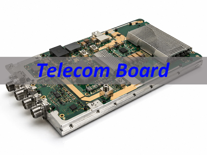
A telecom board supports signal transfer, power control, data exchange, and network communication inside telecom equipment. It may look like a common PCB, but it often needs tighter control over layout, materials, impedance, assembly, and testing. Therefore, engineers and buyers should understand how each manufacturing step affects final performance. In this guide, we explain what a telecom board is, where it works, what layout details matter, how manufacturers build it, and how EBest Circuit supports telecom PCB fabrication and assembly from prototype to production.
What Is a Telecom Board?
A telecom board is a printed circuit board for communication equipment. People may also call it a telecommunications board, telecom PCB, or telecom circuit board.
In simple terms, this board helps electronic devices send, receive, process, or control communication signals. These signals may come from RF modules, optical devices, routers, switches, gateways, or wireless systems.
Unlike a simple control board, a telecom board often needs better signal control. For example, it may need controlled impedance, stable grounding, low signal loss, clean power delivery, or high-speed data routing. Also, many telecom products run for long hours. So, the board must support stable operation over time.
A telecom board can use different structures. It may be a standard FR4 PCB, a high-frequency PCB, a multilayer PCB, a rigid-flex PCB, or a metal core PCB. The right choice depends on the product design, working frequency, heat level, size, and assembly needs.
In real production, a good telecom board does not depend on one factor alone. Instead, it comes from a full process. Layout review, material selection, stack-up control, PCB fabrication, component sourcing, SMT assembly, inspection, and testing all matter.
Item
What It Means for a Telecom Board
Signal transmission
The board must support clean and stable signal paths.
Power control
The board must deliver steady power to ICs, RF parts, and modules.
Material choice
The laminate must match frequency, loss, heat, and cost needs.
Assembly quality
Components must be placed and soldered with good process control.
Testing
Electrical, impedance, AOI, X-ray, and functional tests help confirm quality.
Telecom Board vs Telecommunications Board: Are They the Same?
In most PCB manufacturing contexts, telecom board and telecommunications board mean nearly the same thing. Both refer to circuit boards for communication products.
However, the word “board” can create confusion. In some searches, a telecom board may mean a cable installation backer board. In other searches, it may mean a company board of directors or a telecom job board. Because of this, a PCB article should make the meaning clear from the beginning.
In this article, a telecom board means a PCB or PCBA for electronic communication equipment.
Term
Common Meaning
In This Article
Telecom board
A short term with several possible meanings
A PCB or PCBA used in telecom equipment
Telecommunications board
A more formal term
A circuit board for communication systems
Telecom PCB
A clear manufacturing term
A bare printed circuit board for telecom use
Telecom PCBA
An assembled board
A telecom PCB with components mounted on it
The shorter term telecom board sounds more common and easier to search. The term telecommunications board sounds more formal. Still, both can describe the same product type when we talk about PCB manufacturing.
For buyers, the name matters less than the actual requirement. A real telecommunications board must support stable signal paths, reliable solder joints, suitable materials, and repeatable production quality. Therefore, the focus should stay on engineering and manufacturing details.
What Are Telecom Circuit Boards Used For?
Telecom circuit boards work in many communication systems. Some boards process high-speed digital signals. Some handle RF signals. Others manage power, interfaces, control logic, or network connections.
Application
Common Board Function
Typical PCB Requirement
5G and wireless equipment
Signal transmission, antenna control, RF processing
For example, 5G modules, antenna systems, repeaters, base station parts, and wireless transmission devices often need telecom circuit boards. These boards may require controlled impedance, low-loss materials, and stable copper patterns.
Routers and switches also need telecom boards. These boards support data transfer, power regulation, interface control, and signal processing. Also, they often include BGA chips, Ethernet interfaces, fine-pitch components, and high-speed signal lines.
In industrial communication, gateway boards connect machines, sensors, PLCs, and cloud systems. Therefore, their boards often combine communication interfaces, power circuits, isolation areas, and control units.
As a result, telecom circuit boards cover a wide range of products. However, they share one common goal: they must help communication signals move with stability and low interference.
What Telecom PCB Layout Factors Affect Signal Integrity?
Telecom PCB layout has a strong effect on signal quality. EBest Circuit does not position itself as a full circuit design company. However, we can support layout review, DFM suggestions, stack-up review, impedance coordination, and manufacturability checks.
Before production, engineers should check several layout details.
Split planes, via stitching, reference layer design
RF trace clearance
It reduces noise and coupling.
Distance from power, clock, and digital lines
Via placement
It can affect RF and high-speed signals.
Via count, via position, via type, stub length
Power layout
It supports stable IC operation.
Decoupling placement, power plane design
Assembly clearance
It reduces SMT risk.
Component spacing, pad size, solder mask clearance
Many telecom boards need controlled impedance. This is common in RF lines, Ethernet lines, differential pairs, and high-speed digital interfaces. Trace width, spacing, copper thickness, dielectric thickness, and material type all affect impedance. Therefore, the layout and stack-up should match each other.
Grounding also deserves attention. A clean return path helps signals move with less noise. If a signal crosses a split ground plane, the return path may become unstable. So, ground plane continuity should be checked early.
RF traces need enough distance from noisy power lines, clock signals, and digital circuits. In many telecom PCBs, engineers also use via fences, shielding areas, or grounded copper to improve isolation.
A layout may look perfect in design software. However, real PCB production has tolerances. Etching, drilling, plating, solder mask registration, and lamination can all change final results. Therefore, DFM review helps reduce risk before fabrication.
At EBest Circuit, our layout-related support focuses on practical production checks. We help customers review manufacturability, stack-up feasibility, impedance needs, soldering risks, and assembly clearance.
How Do Telecom Board Manufacturing Processes Support Stable Signal Transmission?
Telecom board performance does not come from layout alone. The manufacturing process also plays a major role. Even small process changes can affect impedance, signal loss, solderability, and long-term stability.
The stack-up defines layer order, dielectric thickness, copper thickness, and reference planes. For controlled impedance boards, stack-up control is very important. EBest can review the stack-up and match it with material and impedance needs.
Signal traces must stay close to the design target. If etching changes the trace width too much, impedance may shift. Therefore, manufacturers need stable imaging and etching control.
Vias also matter. Multilayer telecom boards often include many vias. Accurate drilling helps keep layer connections stable. Also, good hole wall preparation supports reliable copper plating.
Surface finish selection affects assembly quality. Telecom boards may use ENIG, OSP, immersion silver, HASL, or other finishes. ENIG often works well for fine-pitch components and BGA assembly. However, the best finish depends on the product, storage needs, and assembly process.
In short, stable telecom board manufacturing needs tight process control. Each step should support the electrical goal of the board.
What Materials Are Best for High-Frequency Telecom Circuit Boards?
Material choice has a direct effect on telecom board performance. Different products need different materials. Therefore, engineers should not choose a material only by price or habit.
Material Type
Best-Fit Telecom Application
Main Advantage
Standard FR4
Control boards, network boards, low-to-mid frequency boards
Mature process and cost control
High-Tg FR4
Multilayer boards and higher-temperature products
Better thermal stability
Rogers material
RF, microwave, antenna, and high-frequency boards
Lower loss and stable dielectric behavior
PTFE-based laminate
Low-loss RF and microwave boards
Good high-frequency performance
Metal core PCB
Power modules and heat-generating telecom boards
Better heat spreading
Hybrid stack-up
Boards with both RF and digital sections
Balance between cost and performance
FR4 works well for many standard telecom control boards, digital boards, and network interface boards. It offers good cost control, easy sourcing, and mature processing.
High-Tg FR4 supports better thermal stability than standard FR4. It suits multilayer telecom boards, dense assemblies, and products with higher working temperatures.
Rogers laminates are common in RF, antenna, microwave, and high-frequency telecom PCBs. These materials offer more stable dielectric performance and lower signal loss than standard FR4 in many high-frequency designs.
Some RF and microwave boards use PTFE-based materials. These materials can support low-loss signal transmission. However, they need careful fabrication control because they behave differently from FR4.
Some telecom modules generate more heat. For example, power modules or RF amplifier boards may need better thermal paths. In these cases, aluminum or copper base PCBs can help spread heat.
Also, some telecom boards combine FR4 and high-frequency materials. This can reduce cost while keeping RF layers stable. As a result, hybrid stack-ups often work well when only part of the board needs high-frequency performance.
When choosing materials, engineers should review dielectric constant, dissipation factor, copper foil type, Tg, CTE, thermal conductivity, thickness tolerance, and supply stability.
How Does Custom Telecom PCB Assembly Work at EBest?
Telecom PCB assembly at EBest follows a controlled process from files to finished PCBA. This section does not only talk about “reliability.” Instead, it shows the actual assembly flow and process capability.
EBest supports telecom PCB assembly for RF modules, communication control boards, network gateway boards, and other telecom-related products.
Assembly Step
What EBest Does
Customer Benefit
BOM review
Checks part availability, package, lead time, and alternatives
Helps reduce sourcing risk
DFM review
Checks pad size, spacing, polarity, stencil needs, and panelization
Helps reduce SMT issues
Stencil control
Matches stencil design with component packages
Improves solder paste printing
SMT placement
Controls component position and direction
Supports stable assembly quality
Reflow control
Matches temperature profile with board and components
Helps form stable solder joints
BGA/QFN assembly
Handles hidden and fine-pitch packages
Supports dense telecom PCBAs
AOI inspection
Checks visible solder joints and placement
Finds common assembly defects
X-ray inspection
Checks hidden solder joints under BGA/QFN
Improves inspection confidence
Functional testing
Follows customer test requirements
Helps verify board operation
First, EBest reviews the BOM and checks component availability. This step helps customers find supply risks early. Also, it helps confirm package type, part lifecycle, lead time, and possible alternatives.
Next, our team checks assembly-related details. These include pad size, component spacing, solder mask clearance, stencil needs, polarity marks, panelization, and connector placement. As a result, customers can reduce SMT risks before production.
Telecom boards may include QFN, BGA, small passive parts, RF connectors, and shielding parts. Therefore, stencil design and solder paste control matter. Good solder paste printing helps improve solder joint consistency.
During SMT placement, EBest controls component position, feeder setup, package direction, and program accuracy. Then, the reflow profile must match the board and component mix. A proper profile helps form stable solder joints and reduces soldering defects.
Finally, AOI and X-ray inspection help confirm assembly quality. AOI checks visible solder joints, missing parts, polarity, and alignment. X-ray inspection checks hidden solder joints under BGA and QFN packages.
Through this process, EBest helps customers move from bare telecom PCB to assembled PCBA with fewer handoff issues.
Telecom Board Manufacturing Across Communication Applications – EBest Case Studies
EBest Circuit supports telecom board projects across different communication applications. The examples below show how manufacturing choices can support real product needs.
EBest Project Type
Main Challenge
EBest Support
RF communication module board
Signal loss and impedance control
Stack-up review, high-frequency material support, impedance testing
Copper thickness review, thermal via feedback, material suggestions
RF Communication Module Board An RF communication module board often needs controlled impedance, stable material performance, and accurate trace control. For this type of board, EBest focuses on stack-up review, high-frequency material handling, copper thickness control, and impedance testing.
For example, a customer may need an RF board for wireless signal transmission. In this case, material choice and trace accuracy matter. So, EBest reviews the stack-up, confirms the laminate, controls line width, and checks impedance. This helps the board meet the expected signal target.
Industrial Network Gateway PCBA An industrial network gateway often includes processors, memory, power circuits, communication interfaces, connectors, and I/O terminals. Therefore, this project needs both PCB fabrication and PCBA assembly.
For this type of board, EBest can support multilayer PCB production, component sourcing, SMT assembly, AOI, X-ray inspection, and functional testing. In addition, our team can review assembly risks before production. This helps the customer improve production consistency.
Communication Control Board for Equipment Integration Some telecom boards work as control boards inside larger communication equipment. These boards may not use very high RF frequencies. However, they still need stable routing, clean power, reliable solder joints, and good connector strength.
For this type of project, EBest supports prototype builds, small-batch production, and later volume production. Also, we help review material choice, stack-up, DFM issues, assembly process, and testing needs.
High-Power Communication Module Board Some communication modules carry higher current or generate more heat. In these cases, EBest can support copper thickness review, thermal via design feedback, material suggestions, and assembly process control. As a result, the board can handle heat more effectively.
These examples show one point clearly. A telecom board needs more than basic PCB production. It needs careful control from design files to final assembly.
How Do You Choose a Telecom Board Manufacturer?
Choosing a telecom board manufacturer requires more than checking price. A good supplier should understand materials, impedance, fabrication, assembly, testing, and project communication.
Electrical, impedance, AOI, X-ray, functional test
Helps confirm quality before shipment
Production support
Prototype, small batch, mass production
Supports product growth
Communication speed
Clear feedback and practical suggestions
Reduces mistakes and delays
First, check whether the manufacturer has experience with telecom PCBs, RF boards, high-frequency boards, and multilayer boards. Experience helps the supplier find risks faster.
Next, review fabrication capability. The manufacturer should support controlled impedance, multilayer PCB production, fine line control, via plating, surface finishes, and electrical testing.
If your project needs assembly, choose a supplier with SMT assembly, BGA/QFN experience, AOI, X-ray inspection, component sourcing, and testing support.
DFM review is also important. It helps find layout and production risks before manufacturing. This step can save time, especially for dense telecom boards or high-frequency boards.
Finally, consider communication speed. Your supplier should respond clearly, explain risks, and give practical suggestions. This helps reduce mistakes during production.
Why Choose EBest Circuit as Your Telecom Board Manufacturer?
EBest Circuit, also known as Best Technology, supports telecom board customers with PCB fabrication, component sourcing, PCBA assembly, testing, and engineering support.
EBest Capability
How It Helps Telecom Board Projects
One-stop PCB and PCBA service
Customers can manage PCB, components, assembly, and testing with one partner.
EBest supports FR4, High-Tg FR4, Rogers, ceramic, metal core, and special PCB structures.
Component sourcing support
EBest helps check part availability, lead time, package match, and supply risks.
SMT assembly
EBest supports fine-pitch parts, BGA, QFN, connectors, and module-level assembly.
Inspection and testing
AOI, X-ray, electrical testing, and functional testing can support quality control.
Prototype and batch support
Customers can move from sample runs to production with a stable process.
Quality control and traceability
Production records and inspection steps support long-term manufacturing needs.
EBest supports bare PCB fabrication and assembled PCBA production. Therefore, customers can manage PCB, components, assembly, and testing through one manufacturing partner.
EBest can also review manufacturability-related layout details. These include spacing, pad design, solder mask clearance, stack-up feasibility, impedance needs, panelization, and assembly risk. This support is useful for telecom boards with RF traces, dense parts, or mixed signal and power sections.
In addition, EBest has experience with FR4, High-Tg FR4, Rogers materials, ceramic PCBs, metal core PCBs, and other special PCB structures. This helps customers choose a better material path for telecom applications.
For assembly projects, EBest supports SMT assembly for telecom PCBs, including fine-pitch parts, BGA, QFN, connectors, and module-level assemblies. Also, AOI, X-ray inspection, electrical testing, and functional testing can support quality control.
If you need telecom PCB fabrication, telecom PCB assembly, or one-stop telecom board manufacturing support, contact EBest Circuit at sales@bestpcbs.com for a project review or quotation.
FAQs About Telecom Board
1. Is a telecom board the same as a telecom PCB? Yes. In PCB manufacturing, a telecom board usually means a telecom PCB or telecom PCBA for communication equipment.
2. What is the difference between telecom board and telecommunications board? The meaning is usually similar. Telecom board sounds shorter, while telecommunications board sounds more formal.
3. Can FR4 work for telecom circuit boards? Yes. FR4 works for many telecom control boards, network boards, and digital communication boards. For RF or low-loss designs, high-frequency materials may work better.
4. When should a telecom board use Rogers materials? Rogers materials suit RF, microwave, antenna, and high-frequency telecom boards that need lower signal loss and stable dielectric performance.
5. Does every telecom board need impedance control? No. However, boards with RF traces, differential pairs, Ethernet lines, or high-speed signals often need controlled impedance.
6. What does EBest check during telecom PCB layout review? EBest checks manufacturability items such as spacing, stack-up, impedance needs, pad design, solder mask clearance, panelization, via structure, and assembly risk.
7. Can EBest provide telecom PCB assembly? Yes. EBest supports telecom PCB assembly, including SMT assembly, component sourcing, BGA/QFN assembly, AOI, X-ray inspection, and testing support.
8. What files should I provide for a telecom board quotation? You can provide Gerber files, BOM, pick-and-place file, assembly drawing, stack-up requirements, impedance requirements, material preference, quantity, and testing needs.
9. How do I choose a telecom board manufacturer? Choose a supplier with telecom PCB experience, material knowledge, impedance control, PCBA assembly, testing support, DFM review, and clear communication.
PTFE PCB projects usually come with clear business goals: stable RF performance, reliable fabrication, smooth assembly, and fewer delays before production. For buyers, the key question is not only “What is PTFE?” It is also “Can this manufacturer support my material, stack-up, impedance, RF connector assembly, and delivery needs?”
This guide helps you compare PTFE PCB materials, manufacturing capabilities, application fit, DFM support, and supplier selection factors.
What Is a PTFE PCB and Is It Right for Your Project?
A PTFE PCB is a printed circuit board made with PTFE-based dielectric material. Engineers often choose it for RF, microwave, antenna, radar, and high-frequency communication products.
Can the supplier control material, impedance, drilling, and assembly?
When PTFE PCB Is a Good Fit
Your Project Need
Why PTFE Helps
RF signal transmission
Supports lower dielectric loss
Microwave circuit design
Helps keep signal behavior stable
Antenna board development
Supports controlled impedance and phase stability
Radar or communication module
Works well in high-frequency environments
Low-loss signal path
Reduces signal attenuation compared with standard FR4
When FR4 May Still Be Enough
Project Condition
Better Choice
Low-frequency control board
FR4
Cost-sensitive general electronics
FR4
Simple power or LED board
FR4 or MCPCB
RF, microwave, radar, or antenna product
PTFE or other high-frequency laminate
Quick takeaway: Choose PTFE when signal quality matters more than material cost.
What PTFE PCB Materials and Laminates Can You Choose?
Material choice affects loss, impedance, lead time, cost, and long-term reliability. Buyers should not choose a laminate only by brand name. The material should match the frequency, stack-up, copper weight, and production plan.
Material / Laminate Type
Common Use
Buyer Benefit
PTFE Laminate
RF and microwave boards
Low loss and stable electrical behavior
Rogers PTFE-Based Materials
Antenna, radar, telecom, aerospace electronics
Strong RF performance and trusted material data
Taconic Materials
RF modules, microwave circuits, antennas
Good high-frequency options for different budgets
Arlon Materials
RF, military, aerospace, and communication boards
Good fit for demanding high-frequency circuits
Nelco Materials
High-speed and RF-related boards
Useful for signal integrity and stable fabrication
Hybrid PTFE + FR4 Stack-Up
Mixed RF and control circuits
Balances cost, strength, and RF performance
Key Material Properties to Check
Property
Why Buyers Should Care
Dielectric Constant
Affects impedance and signal speed
Dissipation Factor
Affects signal loss
Laminate Thickness
Impacts controlled impedance
Copper Roughness
Influences high-frequency conductor loss
Thermal Stability
Supports reliable soldering and use
Moisture Absorption
Helps keep RF performance stable
Dimensional Stability
Supports drilling, routing, and layer alignment
Practical Material Selection Guide
If Your Product Is…
Consider This Material Direction
Antenna PCB
Low-loss PTFE or Rogers-based laminate
RF module
PTFE laminate with controlled impedance
Microwave board
Low dissipation factor laminate
Radar board
Stable dielectric and tight thickness tolerance
Mixed RF + digital board
Hybrid stack-up may reduce cost
Prototype stage
Choose available materials to shorten lead time
Buyer note: The best material is not always the most expensive one. The best material is the one that matches your RF target, budget, and delivery plan.
PTFE PCB Manufacturing Capabilities at EBest Circuit (Best Technology)
PTFE materials need tighter process control than standard FR4. Drilling, plating, lamination, impedance control, and assembly must work together.
PTFE, Rogers, Taconic, Arlon, Nelco, and other RF laminates
More choices for RF, microwave, antenna, and radar boards
Manufacturing Precision
1–50 layers, 0.4–6.0 mm board thickness, 0.10 mm laser drilling, controlled impedance support
Better signal stability and lower production risk
Quality Certifications
ISO9001, ISO13485, IATF16949, AS9100D quality system support
Suitable for industrial and regulated projects
Turnaround Time
Prototype, small-batch, and volume production support
Faster validation and smoother production planning
Global Sourcing & Delivery
PCB fabrication, component sourcing, PCBA assembly, testing, and delivery
Less supplier coordination and easier project management
What Customers Can Send for Review
File / Information
Why It Helps
Gerber files
Checks circuit pattern and fabrication details
Drill files
Confirms hole size, via design, and plating needs
Stack-up
Confirms layer structure and impedance feasibility
Material request
Checks laminate availability and alternatives
Impedance requirement
Supports controlled RF performance
BOM
Helps with component sourcing and assembly
Pick-and-Place file
Supports SMT assembly preparation
Drawing or special notes
Clarifies tolerance, marking, finish, and testing needs
Manufacturing Items Worth Confirming Early
Laminate brand and grade
Board thickness and tolerance
Copper weight
Controlled impedance target
Minimum trace width and spacing
Minimum hole size
Via structure
Surface finish
RF connector type
Testing requirement
Short takeaway: Good PTFE PCB manufacturing starts before production. Early review helps avoid cost, schedule, and performance issues.
PTFE PCB Solutions for RF, Microwave, Antenna, and Communication Applications
PTFE-based boards serve projects where signal loss, impedance, and frequency stability matter. Buyers often search for a supplier because the product has moved beyond simple FR4 capability.
Application
Common Requirement
How PTFE PCB Helps
RF Modules
Low-loss signal path
Supports stable RF transmission
Microwave Circuits
Controlled signal behavior
Helps reduce dielectric loss
Antenna Boards
Stable impedance and phase
Supports consistent radiation performance
Radar Systems
High-frequency accuracy
Helps with signal stability
Satellite Communication
Reliable RF path
Supports low-loss designs
Wireless Infrastructure
Stable high-frequency operation
Fits RF front-end and antenna systems
Test Equipment
Repeatable signal performance
Supports accurate measurement circuits
Industrial Communication
Reliable signal transfer
Helps in harsh or demanding environments
Application-Based Buying Checklist
Question
Why It Matters
What is the operating frequency?
Helps select the right laminate
What impedance do you need?
Guides stack-up and trace width
Does the board need assembly?
Affects footprint, finish, and PCBA plan
Will the board use RF connectors?
Requires connector launch review
Is the product for prototype or volume?
Affects material choice and lead time
Does the product need special testing?
Impacts cost and delivery schedule
Common RF Board Features
50-ohm transmission lines
Microstrip or stripline structure
Ground via stitching
RF connector launch area
Shielding area
Tight trace control
Low-loss laminate
Stable reference plane
Project note: For RF and microwave boards, the PCB is not only a carrier. It becomes part of the signal path.
PTFE Multilayer PCB Solutions for Complex High-Frequency Projects
Complex RF products often need more than a simple double-sided board. A multilayer PTFE structure can combine RF signal layers, ground planes, power layers, and control circuits.
Multilayer Need
What It Supports
RF Signal Layer
Controlled high-frequency routing
Ground Plane
Better return path and shielding
Power Layer
Stable power distribution
Digital Control Layer
Supports mixed RF and control functions
Via Stitching
Improves grounding around RF areas
Hybrid Stack-Up
Balances cost, RF performance, and strength
Commercial Benefits of PTFE Multilayer Support
Buyer Concern
Multilayer Solution
Board size is too large
More routing layers reduce area
RF and digital circuits need separation
Layer planning improves isolation
Signal path needs stable reference
Ground planes support impedance
Product needs compact design
Multilayer structure supports integration
Cost must stay controlled
Hybrid stack-up can help
Manufacturing Risks to Review
Risk Area
What the Manufacturer Should Check
Layer alignment
Registration between RF and ground layers
Lamination
Bonding material and pressure control
Drilling
Hole quality in PTFE material
Plating
Reliable copper in vias and holes
Impedance
Trace width, dielectric height, and copper thickness
Hybrid structure
CTE difference between PTFE and FR4
Best-Fit Projects
RF modules with dense routing
Antenna control boards
Radar electronics
Microwave communication boards
Mixed RF and digital products
Compact high-frequency assemblies
Buyer note: A multilayer PTFE PCB needs strong front-end engineering review. It should not move directly from file upload to production without stack-up confirmation.
RF Connector Assembly Support for PTFE PCB Projects
RF connectors affect both assembly quality and signal performance. For many high-frequency boards, the connector launch area decides how smoothly the signal enters or leaves the PCB.
RF Connector Item
What to Check
Why It Matters
Connector Type
SMA, SMB, MMCX, U.FL, coaxial connector
Matches frequency, size, and cable interface
Footprint
Pad size, hole size, ground pad, solder mask opening
Supports accurate assembly
Impedance Transition
Connector pin to RF trace
Reduces signal reflection
Ground Via Stitching
Vias near connector ground pads
Improves return path
Mechanical Support
Mounting holes, solder area, board edge
Improves connector strength
Soldering Control
Temperature, alignment, solder volume
Supports stable electrical and mechanical quality
Inspection
Visual check, X-ray, continuity, RF test if required
Short takeaway: RF connector assembly is not a small detail. It directly affects signal quality, board strength, and customer testing results.
DFM Review Support Before PTFE PCB Production
DFM review helps customers find production risks before fabrication starts. For PTFE PCB projects, this step is especially useful because high-frequency boards often have tight material and impedance requirements.
DFM Review Item
What EBest Circuit Checks
Customer Benefit
Material Match
Laminate type, thickness, copper weight
Avoids wrong material selection
Stack-Up
Layer order, dielectric height, bonding material
Supports impedance and reliability
Trace Width / Spacing
Manufacturability and RF routing limits
Reduces production risk
Impedance Target
50-ohm or custom impedance requirements
Improves RF consistency
Via Design
Hole size, annular ring, via placement
Supports plating reliability
Copper Balance
Copper distribution across layers
Helps board flatness
Surface Finish
ENIG or other finish options
Supports soldering and contact quality
RF Connector Area
Footprint, launch, grounding, mechanical support
Improves assembly and signal transition
Panelization
Panel size, breakaway, handling
Supports smoother production
Typical Problems DFM Can Catch
Problem
Possible Impact
Trace width does not match impedance model
RF performance may shift
Via too close to RF trace
Signal path may suffer
Connector pad does not match datasheet
Assembly issue or weak solder joint
Copper area is uneven
Board flatness risk
Stack-up lacks clear reference plane
Poor signal return path
Material is hard to source
Longer lead time
Files Needed for DFM Review
Gerber files
Drill files
Stack-up drawing
Impedance table
Material preference
BOM, if assembly is required
Connector datasheet
Special tolerance notes
Buyer note: DFM review does not replace circuit design. It helps turn your design into a board that the factory can build with better control.
Why Choose EBest Circuit (Best Technology) for PTFE PCB Manufacturing?
Choosing a PTFE PCB supplier should not depend only on price. High-frequency boards need material knowledge, process control, engineering support, and assembly experience.
Customer Need
EBest Circuit Support
High-frequency PCB fabrication
Supports PTFE and RF laminate projects
Material selection help
Reviews Rogers, Taconic, Arlon, Nelco, and other options
Stack-up review
Checks layer structure and impedance feasibility
Controlled impedance
Supports RF and high-speed requirements
DFM before production
Helps reduce manufacturing risks
RF connector assembly
Supports footprint, grounding, soldering, and inspection review
PCBA assembly
Supports SMT, through-hole, sourcing, and testing
Project stages
Supports prototype, small batch, and volume production
Global delivery
Supports overseas customers with one-stop service
Why This Matters for Buyers
Buying Concern
How One-Stop Support Helps
Too many suppliers
PCB, sourcing, assembly, and testing can stay together
Send Gerber files, drill files, stack-up, material request, impedance requirement, quantity, and drawings. For assembly, send BOM and Pick-and-Place files.
Can PTFE PCB use RF connectors?
Yes. RF connectors such as SMA, SMB, MMCX, U.FL, and coaxial types can be assembled when the footprint and grounding design match the connector requirement.
Why does PTFE PCB cost more than FR4?
PTFE laminate costs more. The manufacturing process also needs tighter drilling, plating, lamination, and impedance control.
Can I use Rogers material for PTFE PCB?
Yes. Rogers offers high-frequency materials for RF and microwave products. The right choice depends on frequency, loss target, stack-up, and budget.
Does DFM review help before production?
Yes. It can catch stack-up, impedance, via, connector, copper balance, and manufacturability issues before fabrication.
Can PTFE PCB support prototype and batch production?
Yes. A capable manufacturer can support samples first, then help move the project to small-batch or volume production.
Final Takeaway
If You Need…
Focus On…
Stable RF signal
PTFE laminate, impedance, copper control
Reliable production
DFM review, drilling, plating, lamination
Compact RF design
Multilayer or hybrid stack-up
Complete assembly
RF connector support, SMT, testing
Fewer supplier issues
One-stop PCB + PCBA service
Faster quotation
Complete Gerber, stack-up, BOM, and requirement files
PTFE PCB manufacturing is a project-level decision, not just a material choice. Buyers should check the laminate, stack-up, impedance, RF connector design, DFM support, assembly plan, and supplier capability before production.
EBest Circuit (Best Technology) helps customers move from RF board design files to reliable PCB fabrication and PCBA assembly with practical engineering support.
PTFE PCB plays an important role in RF, microwave, antenna, radar, and high-frequency communication products. Engineers choose PTFE-based circuit boards when they need low signal loss, stable impedance, and reliable high-frequency performance. Compared with standard FR4, PTFE materials offer better electrical stability at higher frequencies. However, material choice alone does not decide the final result. The stack-up, copper design, layout, drilling, plating, surface finish, and manufacturing control also matter. This guide explains what a PTFE PCB is, how PTFE laminate works, what layout factors need attention, and how to choose the right PTFE PCB manufacturer for your project.
What Is a PTFE PCB?
A PTFE PCB is a printed circuit board made with PTFE-based dielectric material. PTFE stands for polytetrafluoroethylene. It has low signal loss, low moisture absorption, strong chemical resistance, and stable electrical behavior.
Engineers often use PTFE boards in RF and microwave circuits. These circuits need better signal control than standard electronic boards. For example, antenna modules, radar boards, satellite communication products, RF amplifiers, and microwave devices often need PTFE materials.
A PTFE board may have one layer, two layers, or many layers. Some projects use pure PTFE laminate. Others combine PTFE with FR4 or other high-frequency materials. This hybrid structure can balance performance, cost, and strength.
PTFE behaves differently from FR4 during fabrication. It needs careful drilling, hole treatment, plating, lamination, and surface preparation. For this reason, a PTFE board requires more process control than a common FR4 board.
In simple terms, PTFE PCB is not just a board with a special material. It is a high-frequency circuit platform. Material, layout, stack-up, and manufacturing process must work together.
Why Do Engineers Use PTFE PCB Material in High-Frequency Circuits?
Engineers use PTFE PCB material because it helps high-frequency signals travel with less loss. At RF and microwave frequencies, the PCB trace acts like a transmission line. Small changes in material or trace shape can affect the signal.
PTFE material offers several key benefits:
Low dielectric constant
Low dissipation factor
Stable signal speed
Low moisture absorption
Good chemical resistance
Strong RF and microwave performance
These features help reduce signal loss. They also help keep impedance more stable. This matters in RF modules, antennas, filters, couplers, radar systems, and communication products.
FR4 works well for many standard electronic products. But it has higher loss at high frequencies. When a product needs cleaner signal transfer, PTFE becomes a better option.
Still, the material does not solve every problem. The layout must match the target impedance. The stack-up must match the design model. The copper thickness, dielectric thickness, via design, and surface finish also affect the final result.
That is why engineers should confirm the material and stack-up before production. Early review can save time and reduce design changes later.
PTFE PCB Laminate: Which Properties Matter Most?
A PTFE PCB laminate should match both electrical and production needs. Many buyers only check the dielectric constant. That is not enough. A good material choice needs a wider review.
Property
Why It Matters
Dielectric Constant
Affects impedance and signal speed
Dissipation Factor
Affects signal loss
Laminate Thickness
Helps control impedance
Copper Roughness
Affects conductor loss at high frequency
Thermal Conductivity
Helps manage heat
Dimensional Stability
Supports accurate layer alignment
Peel Strength
Helps copper stay bonded
Moisture Absorption
Helps keep electrical values stable
Copper Weight
Affects current, loss, and etching control
For RF circuits, dielectric constant and dissipation factor matter most. But copper roughness also plays a big role. At high frequencies, the signal travels near the copper surface. Rough copper can increase loss.
Laminate thickness also needs attention. If the thickness changes too much, impedance can shift. This may affect RF performance.
Before production, customers should confirm the laminate brand, thickness, copper weight, surface finish, and tolerance requirements. For multilayer boards, bonding material also matters.
A good PTFE PCB manufacturer should help review these details. The goal is simple: match the material with the real design and the real production process.
PTFE Teflon PCB vs FR4 PCB: What Is the Difference?
Many people use the term PTFE Teflon PCB when they talk about PTFE-based boards. Teflon is a well-known trade name. PTFE is the material name. In PCB projects, both terms often point to the same type of high-frequency board.
The main difference between PTFE and FR4 is electrical performance. FR4 works well for many common circuit boards. It offers good strength and a lower cost. PTFE offers better signal performance at high frequencies.
Item
PTFE Teflon PCB
FR4 PCB
Main Use
RF and microwave circuits
General electronics
Signal Loss
Lower
Higher at high frequency
Impedance Stability
Better for RF designs
Good for standard boards
Cost
Higher
Lower
Processing Difficulty
Higher
Lower
Typical Products
Antenna, radar, RF module, microwave board
Control board, power board, consumer electronics
You do not need PTFE for every board. If the product works at low speed or low frequency, FR4 may perform well. If the product works in RF or microwave bands, PTFE can give better results.
Some projects use both materials in one board. For example, the RF layer may use PTFE. Other layers may use FR4. This design can reduce cost while keeping RF performance where it matters.
The right choice depends on the frequency, signal loss target, cost target, board structure, and production volume.
How Does a High Frequency PCB with PTFE Improve Signal Performance?
A high frequency PCB with PTFE can improve signal performance by reducing loss and supporting stable impedance. In RF circuits, the board material becomes part of the circuit. The signal does not only travel through copper. It also interacts with the dielectric material around the trace.
PTFE helps in several ways.
First, it has a low dissipation factor. This reduces signal loss. It helps RF signals travel farther with less drop.
Second, it offers stable dielectric behavior. This helps engineers design accurate microstrip, stripline, and coplanar waveguide structures.
Third, it supports better phase stability. This matters in antennas, radar systems, and microwave communication products.
Fourth, it absorbs little moisture. This helps the board keep stable electrical behavior in changing environments.
However, PTFE does not work alone. The manufacturer must also control the board structure. Trace width, copper thickness, dielectric thickness, via position, solder mask, and plating thickness all affect the final result.
For example, a 50-ohm RF trace needs the right width and dielectric height. If the board thickness changes, impedance may shift. If copper plating becomes too thick, the trace shape may also change.
So, high-frequency PCB performance needs both good material and good manufacturing control.
How Should PTFE PCB Layout Be Designed for Stable High-Frequency Performance?
PTFE PCB layout should focus on signal path control, impedance stability, return path quality, and manufacturing feasibility. In many projects, the customer already has the circuit design. The PCB manufacturer mainly helps review the layout from a fabrication and DFM view.
Here are the key layout points.
Controlled Impedance
RF traces often need a clear impedance target, such as 50 ohms. The trace width, copper thickness, dielectric thickness, and ground plane all affect impedance. Before fabrication, the manufacturer should check whether the stack-up can meet the required value.
Short and Clean RF Paths
RF paths should stay as short and direct as possible. Sharp corners, sudden width changes, and long detours can affect signal quality. Smooth trace transitions help support stable performance.
Good Ground Reference
A stable ground plane helps the signal return path. RF layouts often need via stitching near signal paths, connectors, shielding areas, and ground edges. This helps reduce noise and improve RF behavior.
Proper Via Design
Vias affect high-frequency signals. Layout engineers should place RF vias carefully. Ground vias should support the return current path. Signal vias should avoid unnecessary length where possible.
Trace Width and Spacing
PTFE material needs careful process control. Very fine traces and tight spacing should match the manufacturer’s capability. A DFM review can confirm whether the design fits real production limits.
Copper Balance
Copper balance helps control board flatness and lamination behavior. This matters more in PTFE multilayer boards. Uneven copper can make production harder.
RF Connector Footprints
RF connectors need accurate pad size, ground pads, and solder mask clearance. A small footprint issue can affect both assembly and RF performance.
DFM Review Before Fabrication
A strong DFM review can check trace width, spacing, annular ring, via size, impedance stack-up, copper balance, panel design, and surface finish. This step helps turn layout data into a stable physical board.
For EBest Circuit, layout support mainly focuses on manufacturability, stack-up review, impedance feasibility, and production optimization. This helps customers improve the board before fabrication starts.
Rogers PTFE PCB: When Should You Choose Rogers-Based Materials?
A Rogers PTFE PCB can support RF and microwave products that need stable material quality. Rogers offers many high-frequency laminates. Some use PTFE-based systems, while others use different advanced resin systems.
Engineers often choose Rogers materials for:
RF modules
Microwave boards
Antenna circuits
Radar systems
Satellite communication products
Wireless infrastructure
High-speed test equipment
Rogers materials can offer low loss, stable dielectric values, and strong documentation. These features help engineers build more predictable RF products.
But Rogers is not the only option. Some projects may use Taconic, Isola, Panasonic, or other high-frequency materials. The best choice depends on the real application.
Before choosing a Rogers material, check these points:
Operating frequency
Target impedance
Board thickness
Copper weight
Loss requirement
Thermal demand
Layer count
Surface finish
Prototype or mass production plan
A good supplier should not simply suggest the most expensive material. Instead, the supplier should help match the material with performance, cost, and delivery needs.
For many projects, the best material is not the highest-grade material. It is the material that fits the design target and production plan.
Can PTFE Multilayer PCB Support Complex RF Designs?
Yes, PTFE multilayer PCB can support complex RF designs. It can combine RF signal layers, ground planes, power layers, control circuits, and shielding structures in one board.
This structure helps reduce board size. It also improves grounding and signal routing. Many RF modules, antenna systems, radar boards, and communication products use multilayer structures.
A typical PTFE multilayer board may include:
RF signal layers
Solid ground planes
Power layers
Digital control layers
Shielding areas
Via stitching
Hybrid PTFE and FR4 layers
Multilayer PTFE boards need strong process control. PTFE is softer than FR4. It also behaves differently during drilling and lamination. The manufacturer must control drilling, hole treatment, plating, bonding, and layer alignment carefully.
Hybrid stack-ups also need extra review. PTFE and FR4 do not expand in the same way under heat. The stack-up should account for this difference.
For RF products, the layer structure must also support impedance control. The distance between signal trace and reference plane must stay consistent. Copper thickness and dielectric thickness must match the design target.
Before production, customers should share the Gerber files, stack-up, impedance requirements, material choice, and special tolerance needs. This helps the manufacturer review the project clearly.
A PTFE multilayer PCB can work very well when design and production teams align early.
What Should Be Considered for RF Connector Assembly on PTFE PCB?
RF connectors play an important role in PTFE PCB performance. In many RF and microwave boards, the connector is not just a mechanical part. It is also the starting point of the signal path. If the connector footprint, soldering, grounding, or impedance transition is not well controlled, the board may lose part of its high-frequency advantage.
Connector Footprint Accuracy
The RF connector footprint should match the connector datasheet. Pad size, hole size, mounting position, solder mask opening, and ground pad layout all need careful review. For SMA, SMB, MMCX, or other coaxial connectors, even a small footprint error may affect assembly strength and RF performance.
50-Ohm Impedance Transition
Many RF connectors work with a 50-ohm transmission line. The transition from the connector pin to the PCB trace should stay smooth and controlled. Sudden trace width changes, long stubs, or poor pad geometry can create signal reflection. For PTFE PCB, the trace width should match the material thickness, copper thickness, and dielectric constant.
Ground Via Stitching
Good grounding helps the connector perform well. Ground vias should be placed close to the connector ground pads and around the RF launch area. This creates a shorter return path and helps reduce noise, radiation, and signal leakage.
Mechanical Stability
RF connectors often face repeated mating, cable pulling, and vibration. The PCB layout should provide enough copper area, mounting holes, and solder support. For heavier connectors, mechanical reinforcement may be needed to protect the solder joints and board edge.
Soldering Quality
PTFE PCB materials behave differently from FR4 during heating. The assembly process should control the soldering temperature, dwell time, and connector alignment. Clean solder joints help maintain both electrical performance and mechanical strength.
Board Edge and Connector Alignment
Many RF connectors mount at the board edge. The board outline, edge plating, connector position, and panel design should match the assembly requirement. Good alignment helps the cable connect smoothly and reduces mechanical stress.
Inspection After Assembly
After RF connector assembly, the board should be checked for solder quality, connector position, grounding, and mechanical strength. For high-frequency products, visual inspection, X-ray inspection, continuity testing, and RF-related testing may also be required based on the project.
In short, RF connector assembly on PTFE PCB requires close control of both layout and manufacturing details. A good PTFE PCB manufacturer should review the connector footprint, impedance transition, grounding method, soldering process, and inspection plan before production. This helps the final board keep stable RF performance after assembly.
PTFE PCB Manufacturing Capabilities at EBest Circuit (Best Technology)
PTFE PCB manufacturing needs stable material control, precise drilling, reliable plating, and strong impedance management. EBest Circuit (Best Technology) supports PTFE PCB fabrication, DFM review, PCBA assembly, component sourcing, testing, and turnkey electronics manufacturing for RF, microwave, antenna, radar, and communication applications.
Capability
Technical Specification
Business Benefit
Material Coverage
PTFE, Rogers, Taconic, Arlon, Nelco, and other RF laminates
More choices for RF, microwave, antenna, and radar boards
Manufacturing Precision
1–50 layers, 0.4–6.0 mm board thickness, 0.10 mm laser drilling, controlled impedance support
Better signal stability and lower production risk
Quality Certifications
ISO9001, ISO13485, IATF16949, AS9100D quality system support
Suitable for demanding industrial and regulated projects
Turnaround Time
Prototype, small-batch, and volume production support
Faster project validation and smoother production planning
Global Sourcing & Delivery
PCB fabrication, component sourcing, PCBA assembly, testing, and delivery
Less supplier coordination and easier project management
Before production, EBest Circuit can review the material, stack-up, impedance target, trace width, via design, copper thickness, surface finish, and assembly needs. This helps customers reduce design-to-production risks and keep RF performance more stable.
For PTFE PCB projects, the goal is not only to manufacture the board. The goal is to keep the RF signal path stable from layout to final assembly. With DFM support, high-frequency PCB experience, and one-stop PCB/PCBA service, EBest Circuit helps customers move from prototype to reliable production.
Why Choose EBest Circuit (Best Technology) as Your PTFE PCB Manufacturer?
Choosing the right PTFE PCB manufacturer matters because PTFE boards need tighter process control than standard FR4 boards. The supplier should understand high-frequency materials, stack-up control, impedance, drilling, plating, and DFM review.
EBest Circuit (Best Technology) supports PCB fabrication, PCBA assembly, component sourcing, DFM review, testing, and turnkey electronics manufacturing. For PTFE and high-frequency PCB projects, the team can help review material choice, stack-up, impedance targets, layout feasibility, and production details.
Here are the main advantages.
High-Frequency PCB Experience
EBest Circuit works with high-frequency PCB materials for RF, microwave, antenna, communication, industrial control, automotive electronics, aerospace/UAV, and other electronic products.
DFM Review Before Production
The engineering team can review Gerber files, stack-up, trace width, spacing, via design, copper balance, impedance needs, and panel layout. This helps customers find possible issues before fabrication.
Controlled Impedance Support
Many PTFE boards need controlled impedance. EBest Circuit can help check the stack-up and production feasibility based on the target impedance.
PCB Fabrication and PCBA Assembly
Some customers need bare boards only. Others need complete assembly. EBest Circuit can support PCB fabrication, component sourcing, SMT assembly, through-hole assembly, testing, and box-build assembly.
Prototype to Batch Production
Many high-frequency projects start with samples. After testing, they move to small batch or volume production. EBest Circuit can support different stages with stable process control.
Quality and Traceability
EBest Circuit focuses on quality control, process records, and production traceability. This helps customers in industries that need stable documentation and reliable manufacturing support.
Clear Engineering Communication
High-frequency boards need clear communication. Small details can affect the final result. The team can discuss material, stack-up, tolerance, surface finish, assembly needs, and delivery plan with customers before production.
If you need PTFE PCB fabrication or turnkey assembly support, you can send Gerber files, stack-up, BOM, drawings, and technical requirements to sales@bestpcbs.com for review and quotation.
To summarize, a PTFE PCB is a strong choice for RF, microwave, antenna, radar, and high-frequency communication products. It helps reduce signal loss and supports stable electrical performance.
Still, the final result depends on more than material. The layout, stack-up, copper design, drilling, plating, surface finish, and assembly process all matter.
For high-frequency projects, an experienced PTFE PCB manufacturer can help make the process smoother. With early material review, layout checking, DFM support, and controlled fabrication, customers can move from prototype to production with more confidence.
FAQs About PTFE PCB
Q1: Is PTFE PCB only for RF circuits? A1: PTFE PCB mainly serves RF, microwave, antenna, radar, and communication circuits. Some high-speed or low-loss products also use PTFE materials.
Q2: Is PTFE always better than FR4? A2: No. PTFE works better for high-frequency and low-loss circuits. FR4 still works well for many standard electronic products. The best choice depends on frequency, cost, structure, and performance goals.
Q3: What files should I send for a PTFE PCB quote? A3: You can send Gerber files, drill files, stack-up, board thickness, copper weight, surface finish, impedance needs, quantity, and special tolerance requirements. If you need assembly, also send the BOM and Pick-and-Place files.
Q4: Can PTFE PCB support SMT assembly? A4: Yes. PTFE boards can support SMT assembly. The process should consider board thickness, material behavior, component type, soldering profile, and panel handling.
Q5: Which surface finish works well for PTFE PCB? A5: ENIG often works well because it gives a flat and solderable surface. Other finishes may also fit some projects, depending on soldering, bonding, cost, and product needs.
Q6: Why does PTFE PCB cost more than FR4 PCB? A6: PTFE materials cost more. The production process also needs tighter control. Drilling, hole treatment, plating, lamination, and impedance control all require more care.
Q7: Can PTFE work with FR4 in one board? A7: Yes. Many designs use PTFE and FR4 together. This hybrid stack-up can balance RF performance, strength, board thickness, and cost.
Q8: How can I reduce risk before production? A8: Confirm the material, stack-up, impedance target, copper thickness, via design, surface finish, and layout details early. A DFM review can help find issues before fabrication.
This website uses cookies to enhance your experience, remember your preferences, and help us understand how visitors use our site. You can accept all cookies, reject non-essential cookies, or manage your settings.
This website uses cookies to improve your experience while you navigate through the website. Out of these cookies, the cookies that are categorized as necessary are stored on your browser as they are essential for the working of basic functionalities of the website. We also use third-party cookies that help us analyze and understand how you use this website. These cookies will be stored in your browser only with your consent. You also have the option to opt-out of these cookies. But opting out of some of these cookies may have an effect on your browsing experience.
Necessary cookies are absolutely essential for the website to function properly. These cookies ensure basic functionalities and security features of the website, anonymously.
Cookie
Duration
Description
cookielawinfo-checkbox-analytics
11 months
This cookie is set by GDPR Cookie Consent plugin. The cookie is used to store the user consent for the cookies in the category "Analytics".
cookielawinfo-checkbox-functional
11 months
The cookie is set by GDPR cookie consent to record the user consent for the cookies in the category "Functional".
cookielawinfo-checkbox-necessary
11 months
This cookie is set by GDPR Cookie Consent plugin. The cookies is used to store the user consent for the cookies in the category "Necessary".
cookielawinfo-checkbox-others
11 months
This cookie is set by GDPR Cookie Consent plugin. The cookie is used to store the user consent for the cookies in the category "Other.
cookielawinfo-checkbox-performance
11 months
This cookie is set by GDPR Cookie Consent plugin. The cookie is used to store the user consent for the cookies in the category "Performance".
viewed_cookie_policy
11 months
The cookie is set by the GDPR Cookie Consent plugin and is used to store whether or not user has consented to the use of cookies. It does not store any personal data.
Functional cookies help to perform certain functionalities like sharing the content of the website on social media platforms, collect feedbacks, and other third-party features.
Performance cookies are used to understand and analyze the key performance indexes of the website which helps in delivering a better user experience for the visitors.
Analytical cookies are used to understand how visitors interact with the website. These cookies help provide information on metrics the number of visitors, bounce rate, traffic source, etc.
Advertisement cookies are used to provide visitors with relevant ads and marketing campaigns. These cookies track visitors across websites and collect information to provide customized ads.