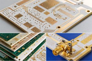
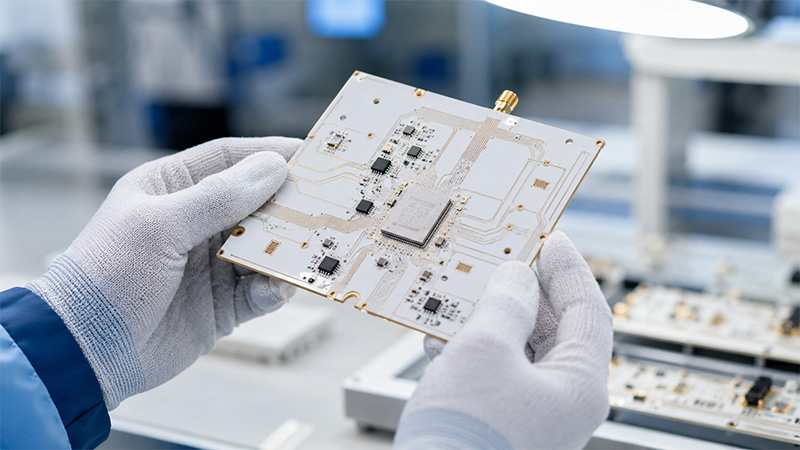
PTFE PCB plays an important role in RF, microwave, antenna, radar, and high-frequency communication products. Engineers choose PTFE-based circuit boards when they need low signal loss, stable impedance, and reliable high-frequency performance. Compared with standard FR4, PTFE materials offer better electrical stability at higher frequencies. However, material choice alone does not decide the final result. The stack-up, copper design, layout, drilling, plating, surface finish, and manufacturing control also matter. This guide explains what a PTFE PCB is, how PTFE laminate works, what layout factors need attention, and how to choose the right PTFE PCB manufacturer for your project.
What Is a PTFE PCB?
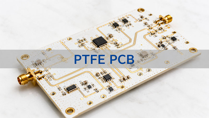
A PTFE PCB is a printed circuit board made with PTFE-based dielectric material. PTFE stands for polytetrafluoroethylene. It has low signal loss, low moisture absorption, strong chemical resistance, and stable electrical behavior.
Engineers often use PTFE boards in RF and microwave circuits. These circuits need better signal control than standard electronic boards. For example, antenna modules, radar boards, satellite communication products, RF amplifiers, and microwave devices often need PTFE materials.
A PTFE board may have one layer, two layers, or many layers. Some projects use pure PTFE laminate. Others combine PTFE with FR4 or other high-frequency materials. This hybrid structure can balance performance, cost, and strength.
PTFE behaves differently from FR4 during fabrication. It needs careful drilling, hole treatment, plating, lamination, and surface preparation. For this reason, a PTFE board requires more process control than a common FR4 board.
In simple terms, PTFE PCB is not just a board with a special material. It is a high-frequency circuit platform. Material, layout, stack-up, and manufacturing process must work together.
Why Do Engineers Use PTFE PCB Material in High-Frequency Circuits?
Engineers use PTFE PCB material because it helps high-frequency signals travel with less loss. At RF and microwave frequencies, the PCB trace acts like a transmission line. Small changes in material or trace shape can affect the signal.
PTFE material offers several key benefits:
- Low dielectric constant
- Low dissipation factor
- Stable signal speed
- Low moisture absorption
- Good chemical resistance
- Strong RF and microwave performance
These features help reduce signal loss. They also help keep impedance more stable. This matters in RF modules, antennas, filters, couplers, radar systems, and communication products.
FR4 works well for many standard electronic products. But it has higher loss at high frequencies. When a product needs cleaner signal transfer, PTFE becomes a better option.
Still, the material does not solve every problem. The layout must match the target impedance. The stack-up must match the design model. The copper thickness, dielectric thickness, via design, and surface finish also affect the final result.
That is why engineers should confirm the material and stack-up before production. Early review can save time and reduce design changes later.
PTFE PCB Laminate: Which Properties Matter Most?
A PTFE PCB laminate should match both electrical and production needs. Many buyers only check the dielectric constant. That is not enough. A good material choice needs a wider review.
| Property | Why It Matters |
|---|---|
| Dielectric Constant | Affects impedance and signal speed |
| Dissipation Factor | Affects signal loss |
| Laminate Thickness | Helps control impedance |
| Copper Roughness | Affects conductor loss at high frequency |
| Thermal Conductivity | Helps manage heat |
| Dimensional Stability | Supports accurate layer alignment |
| Peel Strength | Helps copper stay bonded |
| Moisture Absorption | Helps keep electrical values stable |
| Copper Weight | Affects current, loss, and etching control |
For RF circuits, dielectric constant and dissipation factor matter most. But copper roughness also plays a big role. At high frequencies, the signal travels near the copper surface. Rough copper can increase loss.
Laminate thickness also needs attention. If the thickness changes too much, impedance can shift. This may affect RF performance.
Before production, customers should confirm the laminate brand, thickness, copper weight, surface finish, and tolerance requirements. For multilayer boards, bonding material also matters.
A good PTFE PCB manufacturer should help review these details. The goal is simple: match the material with the real design and the real production process.
PTFE Teflon PCB vs FR4 PCB: What Is the Difference?
Many people use the term PTFE Teflon PCB when they talk about PTFE-based boards. Teflon is a well-known trade name. PTFE is the material name. In PCB projects, both terms often point to the same type of high-frequency board.
The main difference between PTFE and FR4 is electrical performance. FR4 works well for many common circuit boards. It offers good strength and a lower cost. PTFE offers better signal performance at high frequencies.
| Item | PTFE Teflon PCB | FR4 PCB |
|---|---|---|
| Main Use | RF and microwave circuits | General electronics |
| Signal Loss | Lower | Higher at high frequency |
| Impedance Stability | Better for RF designs | Good for standard boards |
| Cost | Higher | Lower |
| Processing Difficulty | Higher | Lower |
| Typical Products | Antenna, radar, RF module, microwave board | Control board, power board, consumer electronics |
You do not need PTFE for every board. If the product works at low speed or low frequency, FR4 may perform well. If the product works in RF or microwave bands, PTFE can give better results.
Some projects use both materials in one board. For example, the RF layer may use PTFE. Other layers may use FR4. This design can reduce cost while keeping RF performance where it matters.
The right choice depends on the frequency, signal loss target, cost target, board structure, and production volume.
How Does a High Frequency PCB with PTFE Improve Signal Performance?
A high frequency PCB with PTFE can improve signal performance by reducing loss and supporting stable impedance. In RF circuits, the board material becomes part of the circuit. The signal does not only travel through copper. It also interacts with the dielectric material around the trace.
PTFE helps in several ways.
First, it has a low dissipation factor. This reduces signal loss. It helps RF signals travel farther with less drop.
Second, it offers stable dielectric behavior. This helps engineers design accurate microstrip, stripline, and coplanar waveguide structures.
Third, it supports better phase stability. This matters in antennas, radar systems, and microwave communication products.
Fourth, it absorbs little moisture. This helps the board keep stable electrical behavior in changing environments.
However, PTFE does not work alone. The manufacturer must also control the board structure. Trace width, copper thickness, dielectric thickness, via position, solder mask, and plating thickness all affect the final result.
For example, a 50-ohm RF trace needs the right width and dielectric height. If the board thickness changes, impedance may shift. If copper plating becomes too thick, the trace shape may also change.
So, high-frequency PCB performance needs both good material and good manufacturing control.
How Should PTFE PCB Layout Be Designed for Stable High-Frequency Performance?
PTFE PCB layout should focus on signal path control, impedance stability, return path quality, and manufacturing feasibility. In many projects, the customer already has the circuit design. The PCB manufacturer mainly helps review the layout from a fabrication and DFM view.
Here are the key layout points.
Controlled Impedance
RF traces often need a clear impedance target, such as 50 ohms. The trace width, copper thickness, dielectric thickness, and ground plane all affect impedance. Before fabrication, the manufacturer should check whether the stack-up can meet the required value.
Short and Clean RF Paths
RF paths should stay as short and direct as possible. Sharp corners, sudden width changes, and long detours can affect signal quality. Smooth trace transitions help support stable performance.
Good Ground Reference
A stable ground plane helps the signal return path. RF layouts often need via stitching near signal paths, connectors, shielding areas, and ground edges. This helps reduce noise and improve RF behavior.
Proper Via Design
Vias affect high-frequency signals. Layout engineers should place RF vias carefully. Ground vias should support the return current path. Signal vias should avoid unnecessary length where possible.
Trace Width and Spacing
PTFE material needs careful process control. Very fine traces and tight spacing should match the manufacturer’s capability. A DFM review can confirm whether the design fits real production limits.
Copper Balance
Copper balance helps control board flatness and lamination behavior. This matters more in PTFE multilayer boards. Uneven copper can make production harder.
RF Connector Footprints
RF connectors need accurate pad size, ground pads, and solder mask clearance. A small footprint issue can affect both assembly and RF performance.
DFM Review Before Fabrication
A strong DFM review can check trace width, spacing, annular ring, via size, impedance stack-up, copper balance, panel design, and surface finish. This step helps turn layout data into a stable physical board.
For EBest Circuit, layout support mainly focuses on manufacturability, stack-up review, impedance feasibility, and production optimization. This helps customers improve the board before fabrication starts.
Rogers PTFE PCB: When Should You Choose Rogers-Based Materials?
A Rogers PTFE PCB can support RF and microwave products that need stable material quality. Rogers offers many high-frequency laminates. Some use PTFE-based systems, while others use different advanced resin systems.
Engineers often choose Rogers materials for:
- RF modules
- Microwave boards
- Antenna circuits
- Radar systems
- Satellite communication products
- Wireless infrastructure
- High-speed test equipment
Rogers materials can offer low loss, stable dielectric values, and strong documentation. These features help engineers build more predictable RF products.
But Rogers is not the only option. Some projects may use Taconic, Isola, Panasonic, or other high-frequency materials. The best choice depends on the real application.
Before choosing a Rogers material, check these points:
- Operating frequency
- Target impedance
- Board thickness
- Copper weight
- Loss requirement
- Thermal demand
- Layer count
- Surface finish
- Prototype or mass production plan
A good supplier should not simply suggest the most expensive material. Instead, the supplier should help match the material with performance, cost, and delivery needs.
For many projects, the best material is not the highest-grade material. It is the material that fits the design target and production plan.
Can PTFE Multilayer PCB Support Complex RF Designs?
Yes, PTFE multilayer PCB can support complex RF designs. It can combine RF signal layers, ground planes, power layers, control circuits, and shielding structures in one board.
This structure helps reduce board size. It also improves grounding and signal routing. Many RF modules, antenna systems, radar boards, and communication products use multilayer structures.
A typical PTFE multilayer board may include:
- RF signal layers
- Solid ground planes
- Power layers
- Digital control layers
- Shielding areas
- Via stitching
- Hybrid PTFE and FR4 layers
Multilayer PTFE boards need strong process control. PTFE is softer than FR4. It also behaves differently during drilling and lamination. The manufacturer must control drilling, hole treatment, plating, bonding, and layer alignment carefully.
Hybrid stack-ups also need extra review. PTFE and FR4 do not expand in the same way under heat. The stack-up should account for this difference.
For RF products, the layer structure must also support impedance control. The distance between signal trace and reference plane must stay consistent. Copper thickness and dielectric thickness must match the design target.
Before production, customers should share the Gerber files, stack-up, impedance requirements, material choice, and special tolerance needs. This helps the manufacturer review the project clearly.
A PTFE multilayer PCB can work very well when design and production teams align early.
What Should Be Considered for RF Connector Assembly on PTFE PCB?
RF connectors play an important role in PTFE PCB performance. In many RF and microwave boards, the connector is not just a mechanical part. It is also the starting point of the signal path. If the connector footprint, soldering, grounding, or impedance transition is not well controlled, the board may lose part of its high-frequency advantage.
Connector Footprint Accuracy
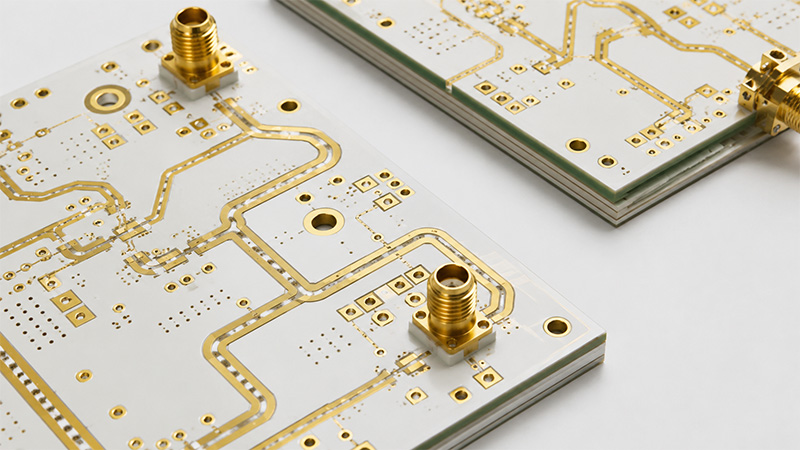
The RF connector footprint should match the connector datasheet. Pad size, hole size, mounting position, solder mask opening, and ground pad layout all need careful review. For SMA, SMB, MMCX, or other coaxial connectors, even a small footprint error may affect assembly strength and RF performance.
50-Ohm Impedance Transition
Many RF connectors work with a 50-ohm transmission line. The transition from the connector pin to the PCB trace should stay smooth and controlled. Sudden trace width changes, long stubs, or poor pad geometry can create signal reflection. For PTFE PCB, the trace width should match the material thickness, copper thickness, and dielectric constant.
Ground Via Stitching
Good grounding helps the connector perform well. Ground vias should be placed close to the connector ground pads and around the RF launch area. This creates a shorter return path and helps reduce noise, radiation, and signal leakage.
Mechanical Stability
RF connectors often face repeated mating, cable pulling, and vibration. The PCB layout should provide enough copper area, mounting holes, and solder support. For heavier connectors, mechanical reinforcement may be needed to protect the solder joints and board edge.
Soldering Quality
PTFE PCB materials behave differently from FR4 during heating. The assembly process should control the soldering temperature, dwell time, and connector alignment. Clean solder joints help maintain both electrical performance and mechanical strength.
Board Edge and Connector Alignment
Many RF connectors mount at the board edge. The board outline, edge plating, connector position, and panel design should match the assembly requirement. Good alignment helps the cable connect smoothly and reduces mechanical stress.
Inspection After Assembly
After RF connector assembly, the board should be checked for solder quality, connector position, grounding, and mechanical strength. For high-frequency products, visual inspection, X-ray inspection, continuity testing, and RF-related testing may also be required based on the project.
In short, RF connector assembly on PTFE PCB requires close control of both layout and manufacturing details. A good PTFE PCB manufacturer should review the connector footprint, impedance transition, grounding method, soldering process, and inspection plan before production. This helps the final board keep stable RF performance after assembly.
PTFE PCB Manufacturing Capabilities at EBest Circuit (Best Technology)
PTFE PCB manufacturing needs stable material control, precise drilling, reliable plating, and strong impedance management. EBest Circuit (Best Technology) supports PTFE PCB fabrication, DFM review, PCBA assembly, component sourcing, testing, and turnkey electronics manufacturing for RF, microwave, antenna, radar, and communication applications.
| Capability | Technical Specification | Business Benefit |
|---|---|---|
| Material Coverage | PTFE, Rogers, Taconic, Arlon, Nelco, and other RF laminates | More choices for RF, microwave, antenna, and radar boards |
| Manufacturing Precision | 1–50 layers, 0.4–6.0 mm board thickness, 0.10 mm laser drilling, controlled impedance support | Better signal stability and lower production risk |
| Quality Certifications | ISO9001, ISO13485, IATF16949, AS9100D quality system support | Suitable for demanding industrial and regulated projects |
| Turnaround Time | Prototype, small-batch, and volume production support | Faster project validation and smoother production planning |
| Global Sourcing & Delivery | PCB fabrication, component sourcing, PCBA assembly, testing, and delivery | Less supplier coordination and easier project management |
Before production, EBest Circuit can review the material, stack-up, impedance target, trace width, via design, copper thickness, surface finish, and assembly needs. This helps customers reduce design-to-production risks and keep RF performance more stable.
For PTFE PCB projects, the goal is not only to manufacture the board. The goal is to keep the RF signal path stable from layout to final assembly. With DFM support, high-frequency PCB experience, and one-stop PCB/PCBA service, EBest Circuit helps customers move from prototype to reliable production.
Why Choose EBest Circuit (Best Technology) as Your PTFE PCB Manufacturer?
Choosing the right PTFE PCB manufacturer matters because PTFE boards need tighter process control than standard FR4 boards. The supplier should understand high-frequency materials, stack-up control, impedance, drilling, plating, and DFM review.
EBest Circuit (Best Technology) supports PCB fabrication, PCBA assembly, component sourcing, DFM review, testing, and turnkey electronics manufacturing. For PTFE and high-frequency PCB projects, the team can help review material choice, stack-up, impedance targets, layout feasibility, and production details.
Here are the main advantages.
High-Frequency PCB Experience
EBest Circuit works with high-frequency PCB materials for RF, microwave, antenna, communication, industrial control, automotive electronics, aerospace/UAV, and other electronic products.
DFM Review Before Production
The engineering team can review Gerber files, stack-up, trace width, spacing, via design, copper balance, impedance needs, and panel layout. This helps customers find possible issues before fabrication.
Controlled Impedance Support
Many PTFE boards need controlled impedance. EBest Circuit can help check the stack-up and production feasibility based on the target impedance.
PCB Fabrication and PCBA Assembly
Some customers need bare boards only. Others need complete assembly. EBest Circuit can support PCB fabrication, component sourcing, SMT assembly, through-hole assembly, testing, and box-build assembly.
Prototype to Batch Production
Many high-frequency projects start with samples. After testing, they move to small batch or volume production. EBest Circuit can support different stages with stable process control.
Quality and Traceability
EBest Circuit focuses on quality control, process records, and production traceability. This helps customers in industries that need stable documentation and reliable manufacturing support.
Clear Engineering Communication
High-frequency boards need clear communication. Small details can affect the final result. The team can discuss material, stack-up, tolerance, surface finish, assembly needs, and delivery plan with customers before production.
If you need PTFE PCB fabrication or turnkey assembly support, you can send Gerber files, stack-up, BOM, drawings, and technical requirements to sales@bestpcbs.com for review and quotation.
To summarize, a PTFE PCB is a strong choice for RF, microwave, antenna, radar, and high-frequency communication products. It helps reduce signal loss and supports stable electrical performance.
Still, the final result depends on more than material. The layout, stack-up, copper design, drilling, plating, surface finish, and assembly process all matter.
For high-frequency projects, an experienced PTFE PCB manufacturer can help make the process smoother. With early material review, layout checking, DFM support, and controlled fabrication, customers can move from prototype to production with more confidence.
FAQs About PTFE PCB
Q1: Is PTFE PCB only for RF circuits?
A1: PTFE PCB mainly serves RF, microwave, antenna, radar, and communication circuits. Some high-speed or low-loss products also use PTFE materials.
Q2: Is PTFE always better than FR4?
A2: No. PTFE works better for high-frequency and low-loss circuits. FR4 still works well for many standard electronic products. The best choice depends on frequency, cost, structure, and performance goals.
Q3: What files should I send for a PTFE PCB quote?
A3: You can send Gerber files, drill files, stack-up, board thickness, copper weight, surface finish, impedance needs, quantity, and special tolerance requirements. If you need assembly, also send the BOM and Pick-and-Place files.
Q4: Can PTFE PCB support SMT assembly?
A4: Yes. PTFE boards can support SMT assembly. The process should consider board thickness, material behavior, component type, soldering profile, and panel handling.
Q5: Which surface finish works well for PTFE PCB?
A5: ENIG often works well because it gives a flat and solderable surface. Other finishes may also fit some projects, depending on soldering, bonding, cost, and product needs.
Q6: Why does PTFE PCB cost more than FR4 PCB?
A6: PTFE materials cost more. The production process also needs tighter control. Drilling, hole treatment, plating, lamination, and impedance control all require more care.
Q7: Can PTFE work with FR4 in one board?
A7: Yes. Many designs use PTFE and FR4 together. This hybrid stack-up can balance RF performance, strength, board thickness, and cost.
Q8: How can I reduce risk before production?
A8: Confirm the material, stack-up, impedance target, copper thickness, via design, surface finish, and layout details early. A DFM review can help find issues before fabrication.