What is HDI PCB fabrication? This guide explores its types, applications, fabrication process, manufacturer recommendation and how to get a quote.
Are you troubled with these problems?
- Are you struggling with design inefficiency caused by high-density routing complexity?
- Are frequent thermal stress cracking issues due to insufficient microvia reliability affecting your production?
- Is yield fluctuation and cost overruns caused by multi-layer alignment accuracy deviation impacting your operations?
As a HDI PCB fabrication manufacturer, EBest Circuit (Best Technology) can provide you service and solutions:
- Customized lamination solutions: Selecting high-Tg substrates and laser microvia technology to achieve ≥98% yield for microvias under 100μm, directly addressing thermal stress cracking challenges.
- Signal integrity optimization package: Providing impedance matching design and dielectric constant control services to ensure ≤5% loss in high-frequency signal transmission, resolving routing complexity issues.
- Flexible capacity matching: 7×12-hour rapid response system, reducing lead time from order placement to prototype delivery to 48 hours, addressing cycle time pressures for multi-variety small-batch orders.
Welcome to contact us if you have any request for HDI PCB fabrication service: sales@bestpcbs.com.
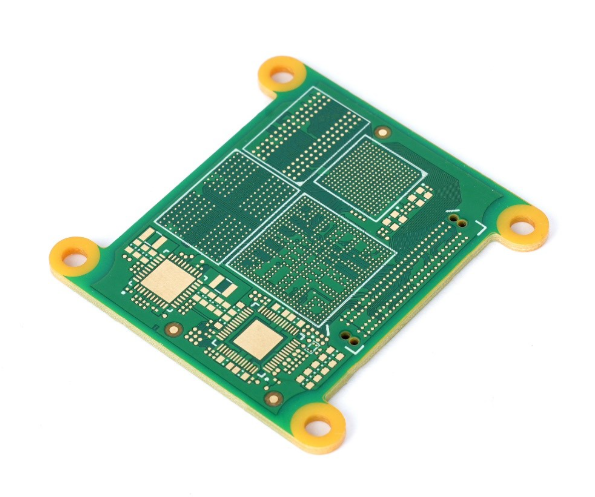
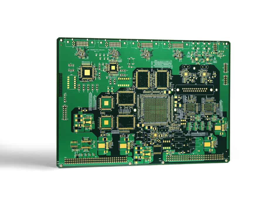
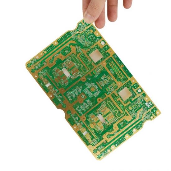
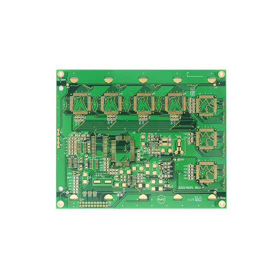
What Is HDI PCB Fabrication?
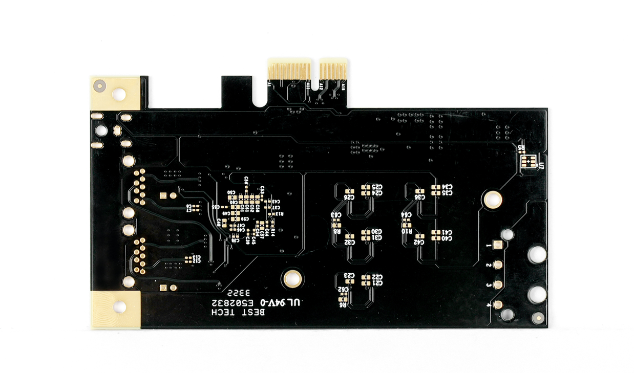
HDI PCB Fabrication is an advanced printed circuit board production technology that achieves significantly higher complex circuit routing and component density in a smaller space by using finer line/spacing, smaller microvias (such as laser-drilled blind and buried vias), and higher layer stack-up structures.
This process is designed to meet the stringent requirements of modern electronic products for miniaturization, lightweight design, high-speed and high-frequency performance, and powerful functionality, providing designers with a reliable interconnect solution to overcome space limitations and realize complex designs.

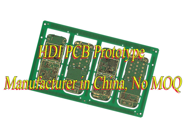
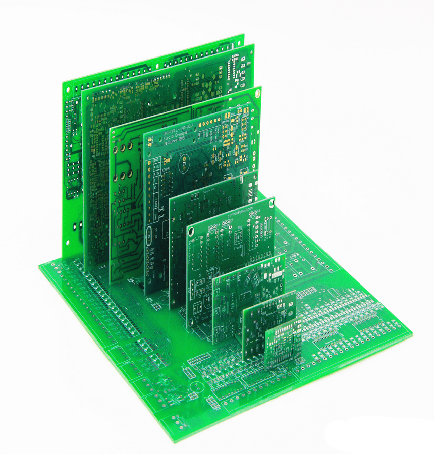
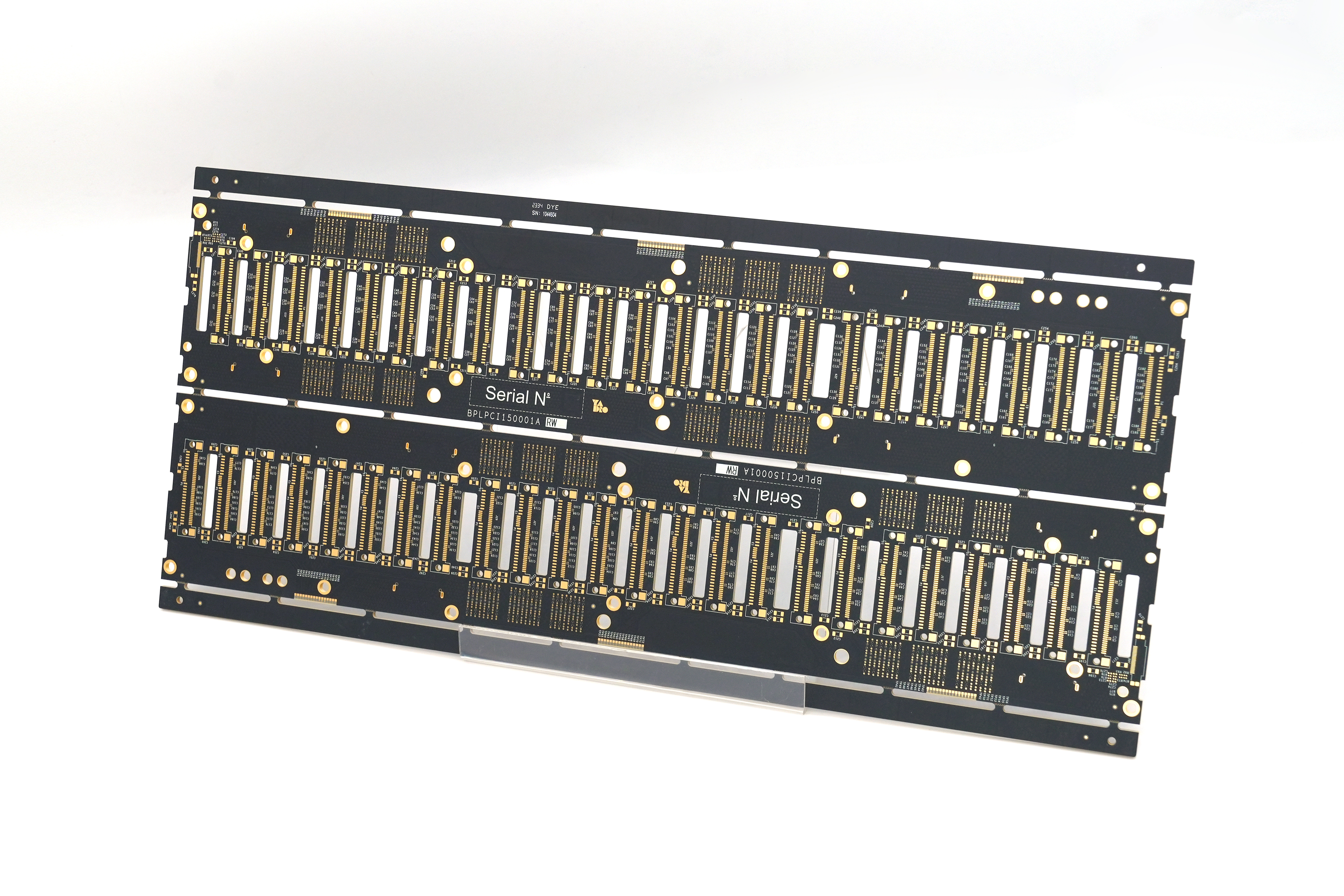
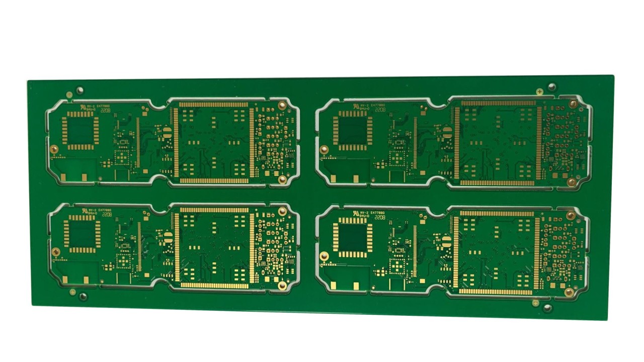
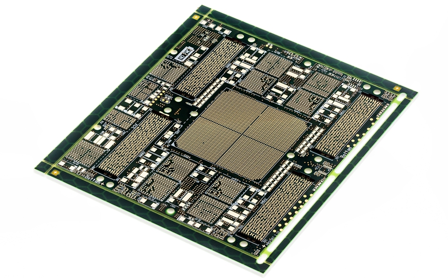
Types of HDI Printed Circuit Board Fabrication
First-order HDI Type I
- Structure Features: Single-layer blind via structure, typically “1+N+1” form. Uses through-hole and blind via only, no buried via. Blind via connects surface layer to inner layer without penetrating the entire board.
- Technical Highlights: Completed through one outer copper foil lamination, one drilling, and one laser drilling.
- Application Scenarios: Suitable for low-complexity applications like cost-sensitive consumer electronics and basic control modules.
- Advantages: Simple process, low cost, meets basic interconnection needs.
Second-order HDI Type II
- Structure Features: Adds buried via based on Type I, forming a 3D interconnection network of through-hole, blind via, and buried via.
- Technical Highlights: Requires two outer copper foil laminations, two drillings, and two laser drillings. Buried via connects internal multi-layer circuits.
- Application Scenarios: Applied in medium-complexity circuits like smartphones, tablets, wearable device motherboards, and mid-range consumer electronics.
- Advantages: Enhanced wiring density and signal transmission capability, supports multi-pin device connections.
Third-order HDI Type III
- Structure Features: Features two or more blind via layers, requiring multiple laser drilling, plating, and lamination processes. Typical forms include “2+N+2” or “3+N+3”.
- Technical Highlights: Uses stacked or staggered blind via designs combined with via-in-pad plating to achieve high-density interconnection. Blind via, buried via, and through-hole work together for complex layer-to-layer connections.
- Application Scenarios: Used in high-density BGA devices, 5G communication equipment, medical imaging devices, automotive electronics, and high-performance scenarios.
- Advantages: High wiring density, low signal loss, excellent thermal management, meets high-speed signal transmission requirements.
Anylayer HDI
- Structure Features: All layers are high-density interconnection layers. Each layer conductor connects freely via stacked via-in-pad micro blind via structures, supporting arbitrary layer-to-layer interconnection.
- Technical Highlights: Adopts modified semi-additive process to achieve fine line width/spacing. Combines laser direct imaging for precision processing.
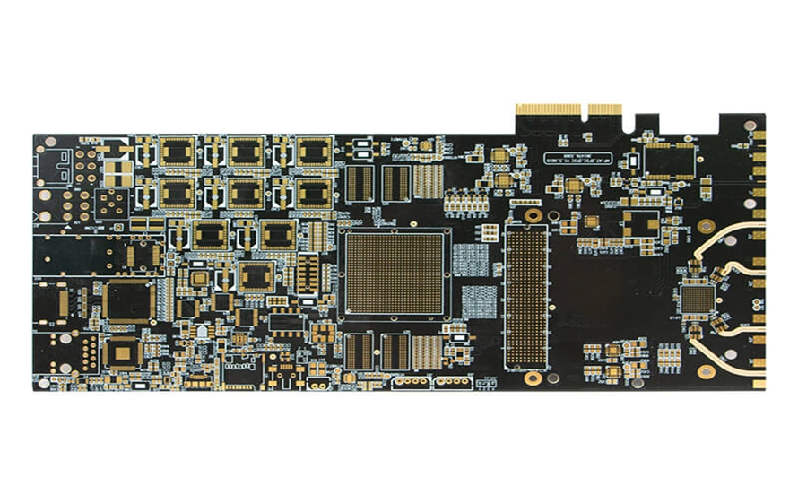
- Application Scenarios: Applied in high-end smartphones, high-performance servers, AI acceleration modules, 5G base stations, and complex industrial control systems.
- Advantages: Ultimate wiring density, flexible design freedom, low signal delay, suitable for ultra-compact, high-integration electronics.
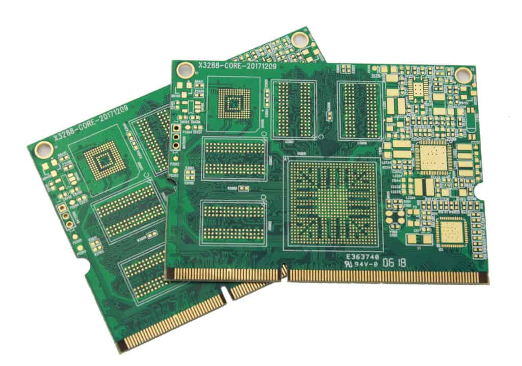
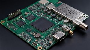
Applications of HDI PCB Fabrication
- Smartphones and Tablets: Applied in motherboard design to support high-density integration of 5G RF modules, AI chips, and other components, enabling compact device designs.
- Wearable Devices: Utilized in smartwatches, earbuds, and similar devices to achieve miniaturization and multifunctional integration through HDI technology.
- Automotive Electronics: Deployed in autonomous driving systems, in-car navigation, millimeter-wave radar, and infotainment systems to ensure high-precision signal transmission.
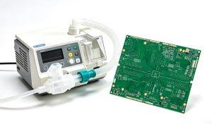
- Medical Equipment: Used in EEG machines, implantable devices, and diagnostic tools requiring high reliability and precision wiring.
- Communication Infrastructure: Essential for 5G base stations, data center switches, and network devices needing high-speed signal processing and multi-layer stacking.
- Industrial Control: Integrated into sensors, industrial printers, and automation systems for stable operation in complex environments.
- Aerospace and Defense: Critical for satellites, missiles, flight recorders, and similar equipment demanding high reliability and extreme durability.
- Consumer Electronics Modules: Applied in drones, IoT devices, and premium cameras to enable multifunctional integration within compact spaces.
HDI PCB Fabrication Process
1. Design & Engineering Preparation
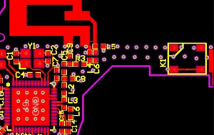
- Circuit Design: Utilize professional EDA software (e.g., Cadence Allegro, Mentor PADS) for schematic design and PCB layout, generating Gerber files, drilling data, and IPC netlists for manufacturing.
- Design for Manufacturability (DFM): Engineers review design files to verify compliance with process capabilities (e.g., trace width/spacing, hole sizes, stack-up structures) and address potential issues through engineering queries (EQ) with clients.
- Process Planning: Determine laser drilling cycles, lamination sequences, and specialized processes (e.g., via filling plating) based on HDI complexity (e.g., 1+N+1, 2+N+2, or any-layer interconnections).
2. Inner Layer Fabrication
- Cutting: Size raw copper-clad laminate (CCL) panels to production dimensions.
- Pre-treatment: Remove copper surface oxides/impurities via mechanical brushing/chemical cleaning to ensure dry film adhesion.
- Lamination & Exposure: Apply photosensitive dry film to copper surfaces, then transfer circuit patterns using UV light through artwork films or LDI (Laser Direct Imaging).
- Development & Etching: Dissolve unexposed dry film with alkaline solution, followed by acidic etching to remove exposed copper, forming inner layer circuits.
- Stripping & AOI Inspection: Remove residual dry film, then perform automatic optical inspection (AOI) to detect defects like opens, shorts, or pinholes.
- Brown Oxide Treatment: Micro-etch copper surfaces to create a uniform organic-metallic layer, enhancing adhesion to prepreg (PP) during lamination.
3. Lamination & Drilling
- Lay-up & Lamination: Align inner core boards, prepreg sheets, and copper foils per stack-up design, then laminate under heat/vacuum to bond layers via cured resin.
- Mechanical Drilling: Create through-holes using carbide drills.
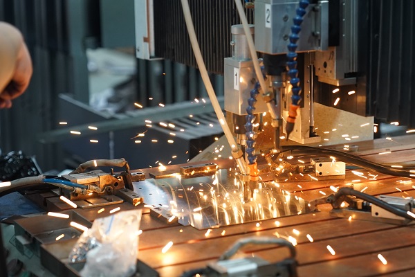
- Laser Drilling: Core HDI process using CO₂/UV lasers to ablate dielectric material, forming microvias/buried vias (<150μm diameter) for high-density routing.
4. Hole Metallization & Plating
- Desmear & Electroless Copper Deposition: Remove drilling residues (smear) with permanganate solutions, then deposit 0.3-0.5μm conductive copper via chemical reduction to enable hole conductivity.
- Electroplating Copper: Electrolytically thicken copper to ≥5-8μm on hole walls/surfaces for mechanical strength/current capacity.
- Via Filling Plating: Fill blind vias with specialized plating chemicals or conductive/insulative resins for planarization, enabling fine-pitch outer layer routing.
5. Outer Layer Fabrication
- Pattern Transfer: Repeat inner-layer-like processes (dry film application, exposure/LDI, development) to create outer layer circuit patterns.
- Pattern Plating: Electroplate additional copper on exposed circuits/vias, often with a thin tin layer as etch resist.
- Etching & Stripping: Remove unprotected copper via etching, then strip tin to reveal final outer layer circuits.
- AOI Inspection: Conduct final AOI to ensure defect-free outer layer circuits.
6. Solder Mask & Surface Finish
- Solder Mask Application: Coat liquid photoimageable solder mask (LPI), cure permanently after exposure/development to expose pads while insulating/protecting circuits.
- Surface Finish: Treat exposed pads for solderability/reliability. Common finishes include:
- ENIG (Electroless Nickel Immersion Gold): Deposit nickel/gold layers for flatness/weldability.
- Immersion Tin: Provide uniform surface/solderability.
- OSP (Organic Solderability Preservative): Apply organic film for cost efficiency (shorter shelf life).
- Silkscreen Printing: Print component identifiers, polarity marks, and logos for assembly/recognition.
7. Formation & Electrical Testing
- Routing/Profiling: CNC mill production panels into individual PCBs or use V-cut/punching methods.
- Electrical Test: Perform 100% open/short testing via flying probe or fixture-based systems to verify electrical integrity per design.
8. Final Inspection & Packaging
- Final Quality Control (FQC): Conduct visual inspection (scratches/copper exposure), dimensional checks, and hole position verification to meet specifications.
- Packaging & Shipping: Clean, vacuum-seal with desiccant, attach inspection reports, and prepare for dispatch.

HDI PCB Fabrication Service We Offered
Here are HDI PCB fabrication service we can provide you:
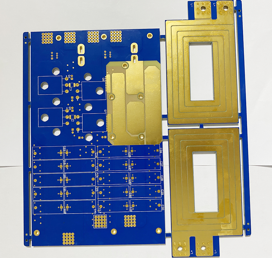
- Precision Design Support: Equipped with a professional engineering team, we provide full-process design support from circuit design optimization, stack-up structure design to signal integrity analysis. We support complex structural designs including blind/buried vias, microvias (starting from 0.1mm diameter), and Via-in-Pad, ensuring design for manufacturability (DFM) and cost control.
- Multi-Stage HDI Process Capability: Our capabilities span from 1+N+1 to any-layer HDI processes, supporting advanced technologies such as fine line width/spacing (≥50μm), back-drilling, copper-filled vias, and laser direct imaging (LDI). These meet the demands of high density, high-frequency, high-speed, and high-thermal dissipation applications.
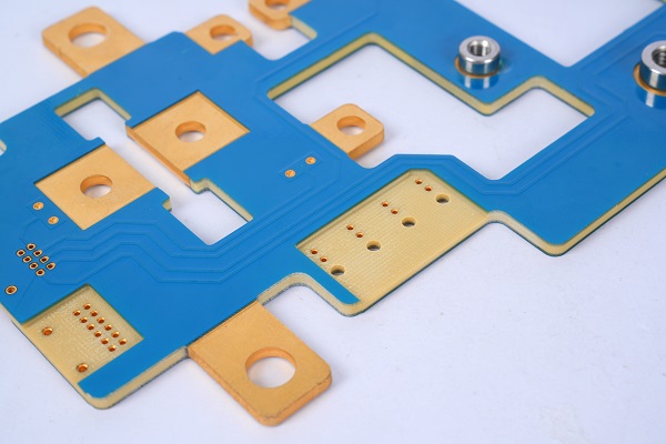
- Diverse Materials and Surface Finishes: We offer a range of material options including high-frequency/high-speed substrates (e.g., PTFE, hydrocarbon resin), high-Tg laminates, and halogen-free materials. Surface finish options include ENIG, ENEPIG, OSP, immersion silver, and immersion tin, catering to various application scenarios.
- Rapid Prototyping and Mass Production Services: With automated production lines and efficient manufacturing systems, we support fast prototyping for new product introduction (NPI) with a turnaround as quick as 48 hours. Our short mass production lead times and flexible capabilities accommodate both small-batch multi-variety and large-batch orders.
- Strict Quality Control System: Certified to international standards such as ISO 9001 and IATF 16949, we employ full-process inspection equipment including AOI, X-ray, flying probe testing, and reliability tests (e.g., thermal shock, thermal humidity cycling) to ensure zero-defect delivery.
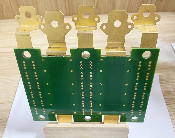
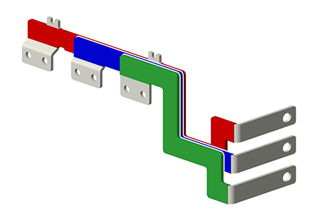
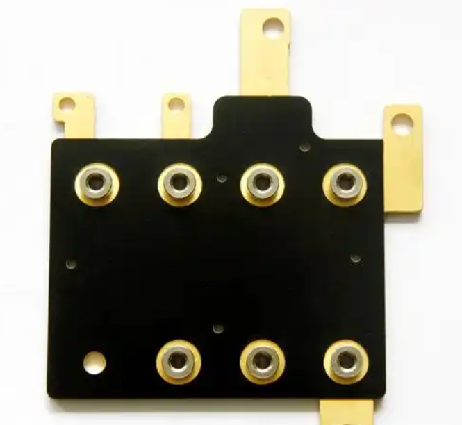
- Customized Solutions: We provide tailored services to meet specific client needs, such as thick-copper HDI (supporting copper thickness over 3oz), rigid-flex HDI, embedded components (e.g., capacitors, resistors), and metal-core HDI. These address the stringent requirements of consumer electronics, automotive electronics, medical devices, aerospace, and other industries.

Why Choose EBest Circuit (Best Technology) as HDI PCB Fabrication Manufacturer?
Below are reasons why choose as HDI PCB fabrication manufacturer:
- 19-Year Experience-Driven Cost Advantage: Leveraging 19 years of HDI PCB production experience, we achieve 15-25% lower prices compared to industry averages through scaled manufacturing and global supply chain collaboration. Transparent pricing and tailored cost-control solutions precisely align with designers’ budget requirements.
- Quality Benchmarks Meeting International Standards: Utilizing Class A substrates and high-precision LDI exposure equipment, our products comply with ISO 9001, IPC-6012, and other global certifications. Microvia precision is controlled within ±0.02mm, and interlayer alignment deviation is ≤5μm, ensuring long-term stability in high-frequency, high-speed applications.
- Comprehensive Quality Control System: Implementing 18 rigorous inspection procedures from raw materials to finished products, we integrate AOI optical inspection, flying probe testing, and X-ray interlayer detection technologies. Defect rates are capped at 0.02%, meeting stringent reliability delivery standards.
- Efficient Delivery Capability: Optimized production scheduling via intelligent management systems reduces standard HDI board lead times to 5-7 days, with urgent orders achievable within 48 hours. Partnering with DHL/UPS international express ensures timely sample delivery to global design hubs.
- Full-Cycle Design and Assembly Services: From PCB layout optimization and DFM analysis to rapid prototyping, SMT assembly, and functional testing, we offer end-to-end solutions. A multilingual engineering team provides 24/7 support, minimizing cross-departmental coordination costs for clients.
- Global Market Access Certifications: Products are certified under UL safety standards, RoHS, and REACH regulations and other international market entry requirements. This accelerates your product certification processes and market deployment.
- Customized Process Solutions: For niche applications like 5G millimeter-wave, automotive ADAS, and medical implants, we provide specialized processes including HDI+AnyLayer, blind/buried vias, and rigid-flex boards, supporting composite applications with high-frequency/high-speed materials such as Taconic/Rogers.
- Green Manufacturing Practices: Adopting lead-free, halogen-free processes and closed-loop wastewater treatment systems, we reduce carbon emissions by 30% compared to industry averages. Compliance with ISO 14001 environmental management standards aligns with ESG procurement demands from international clients.
Our Quality Inspection for HDI PCB Fabrication
- Material Inspection: Conduct rigorous incoming inspection of raw materials including substrate, copper foil, and dielectric layers to ensure key parameters such as dielectric properties, decomposition temperature, and mechanical durability meet design requirements. Inspection covers copper foil thickness (9μm to 400μm), dielectric constant (Dk), loss factor (Df), and glass transition temperature (Tg), preventing signal integrity degradation or thermal reliability issues due to material defects.
- Inner Layer Pattern and Etching Inspection: Utilize Automatic Optical Inspection (AOI) systems to check line width, spacing, alignment, and etching uniformity of inner layer circuits, identifying defects like shorts, opens, or residual copper. High-precision imaging ensures geometric accuracy in fine-pitch areas (e.g., μBGA regions), preventing signal distortion or impedance mismatch.
- Microvia and Drilling Quality Inspection: Employ X-ray and microsectioning techniques to evaluate microvia hole wall quality, copper plating uniformity, and interlayer alignment accuracy. Focus on aspect ratio, debris removal efficacy, and target pad connection integrity to ensure interconnect reliability per IPC-6012 standards.
- Lamination Process Inspection: Verify board thickness uniformity, dielectric layer thickness, and interlayer bonding strength post-lamination. Validate absence of delamination, blisters, or inadequate resin fill via thermal stress testing (e.g., 5-cycle IPC-TM 650-2.6.8 Condition B). Monitor glass-to-resin ratio impact on coefficient of thermal expansion (CTE).
- Surface Finish Inspection: Assess surface coating thickness, flatness, and solderability per application requirements (e.g., ENIG, OSP, HASL). Evaluate coating adhesion via tape peel tests, ensuring soldering yield and long-term oxidation resistance.
- Electrical Performance Testing: Perform continuity testing (opens/shorts), impedance verification, and high-frequency signal integrity validation using flying probe testers or dedicated fixtures. Measure insulation resistance (≥10MΩ), dielectric withstand voltage (≥1000VDC), and humid environment insulation performance (≥500MΩ) per IPC-TM 650 standards to confirm circuit functionality.
- Final Appearance and Dimensional Inspection: Conduct visual checks for warpage, scratches, pad oxidation, and dimensional measurements (hole position accuracy, outline tolerance). Ensure mechanical tolerances within ±0.05mm using optical metrology tools per IPC-A-600 standards, meeting assembly requirements.
- Reliability Testing: Evaluate durability under extreme conditions via thermal cycling (-55°C to +125°C), mechanical vibration, and humid aging tests. Monitor conductor resistance change (≤10%), dielectric integrity, and microvia structural stability to ensure lifecycle performance reliability.
How to Get a Quote for HDI PCB Fabrication Service?
List of materials required for quotation:
- Gerber Files with Layer Stack-up Details
- Bill of Materials (BOM) specifying material types and component specifications
- Via Specifications including microvia, blind via, and buried via counts, sizes, and plating requirements
- Surface Finish Requirements (e.g., ENIG, HASL, Immersion Silver, Gold Plating)
- Impedance Control Specifications for targeted layers or layer pairs
- Minimum Trace Width and Spacing tolerances
- Drill Files and Drill Chart with hole sizes and types
- Solder Mask and Silkscreen color/location specifications
- Material Specifications (e.g., FR4, high-frequency laminates, polyimide substrates, copper foil grades)
- Production Quantity and Volume (prototype vs. mass production)
- Testing Requirements (AOI, X-ray, flying probe test, reliability testing)
- Certification Standards (IPC Class 2/3, RoHS, UL, ISO compliance)
- Special Process Requests (embedded components, thermal management solutions, controlled dielectric thickness)
Welcome to contact us if you have any request for HDI PCB fabrication: sales@bestpcbs.com.