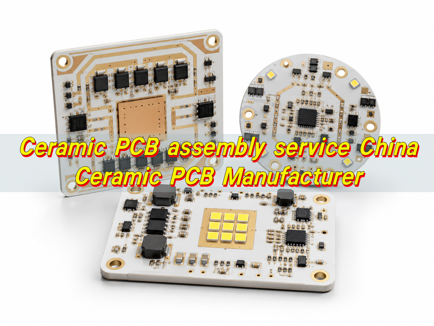
What Is Ceramic PCB Assembly?
Ceramic PCB assembly is the process of mounting electronic components onto a ceramic PCB board and turning it into a working electronic module. The process may include solder paste printing, SMT placement, reflow soldering, through-hole assembly, inspection, electrical testing, functional testing, and final packaging.
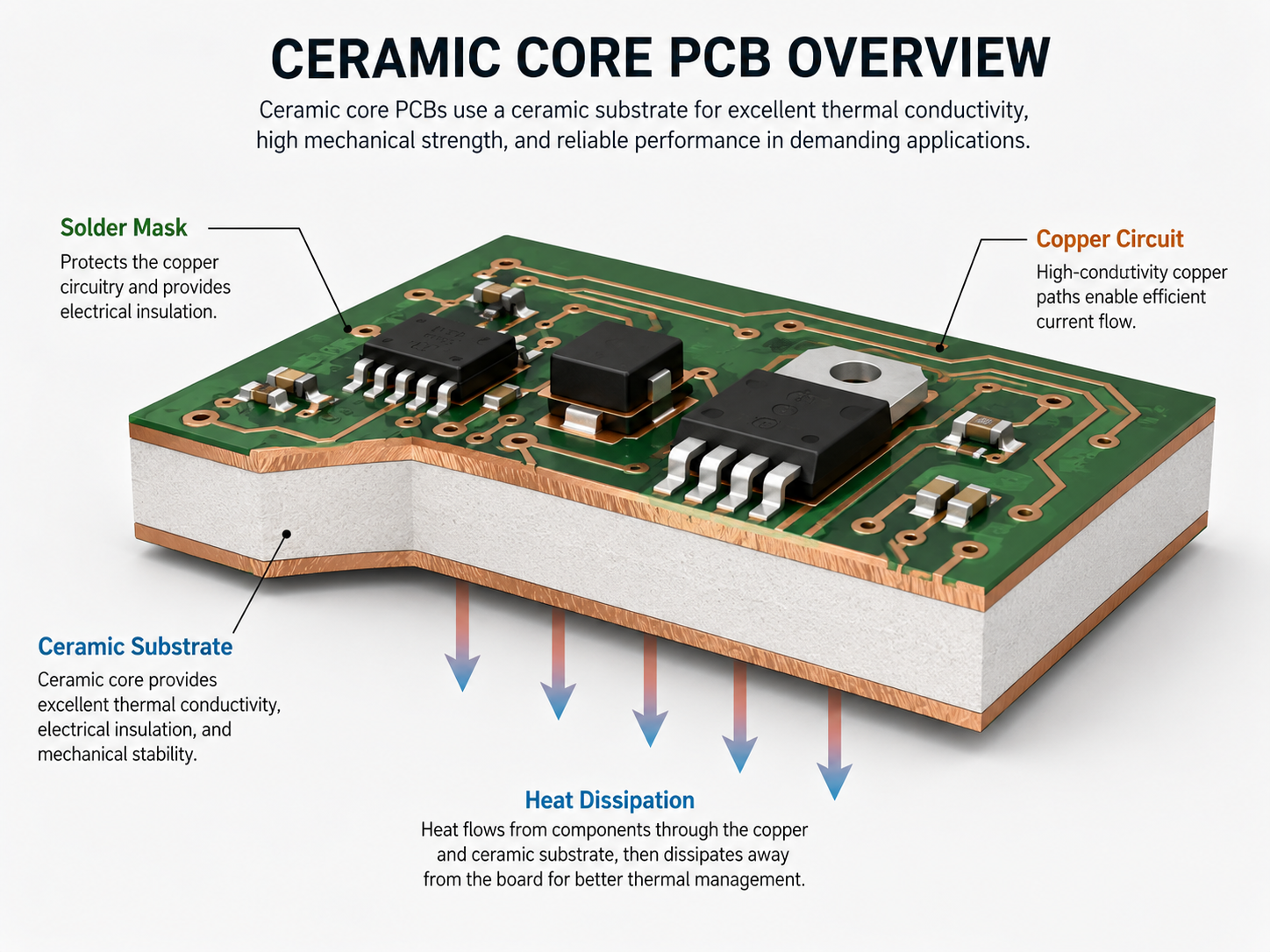
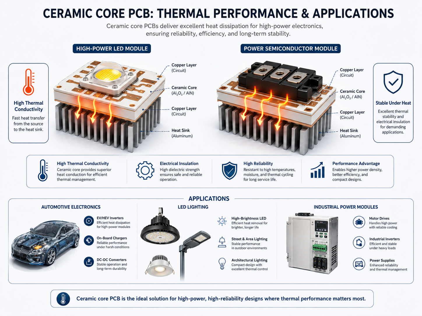
A ceramic PCB is used when a product needs better heat transfer, stable insulation, high dimensional stability, or reliable performance in compact power circuits. These boards are widely used in LED modules, power supplies, automotive electronics, RF products, laser devices, medical equipment, industrial controls, and high-temperature electronics.
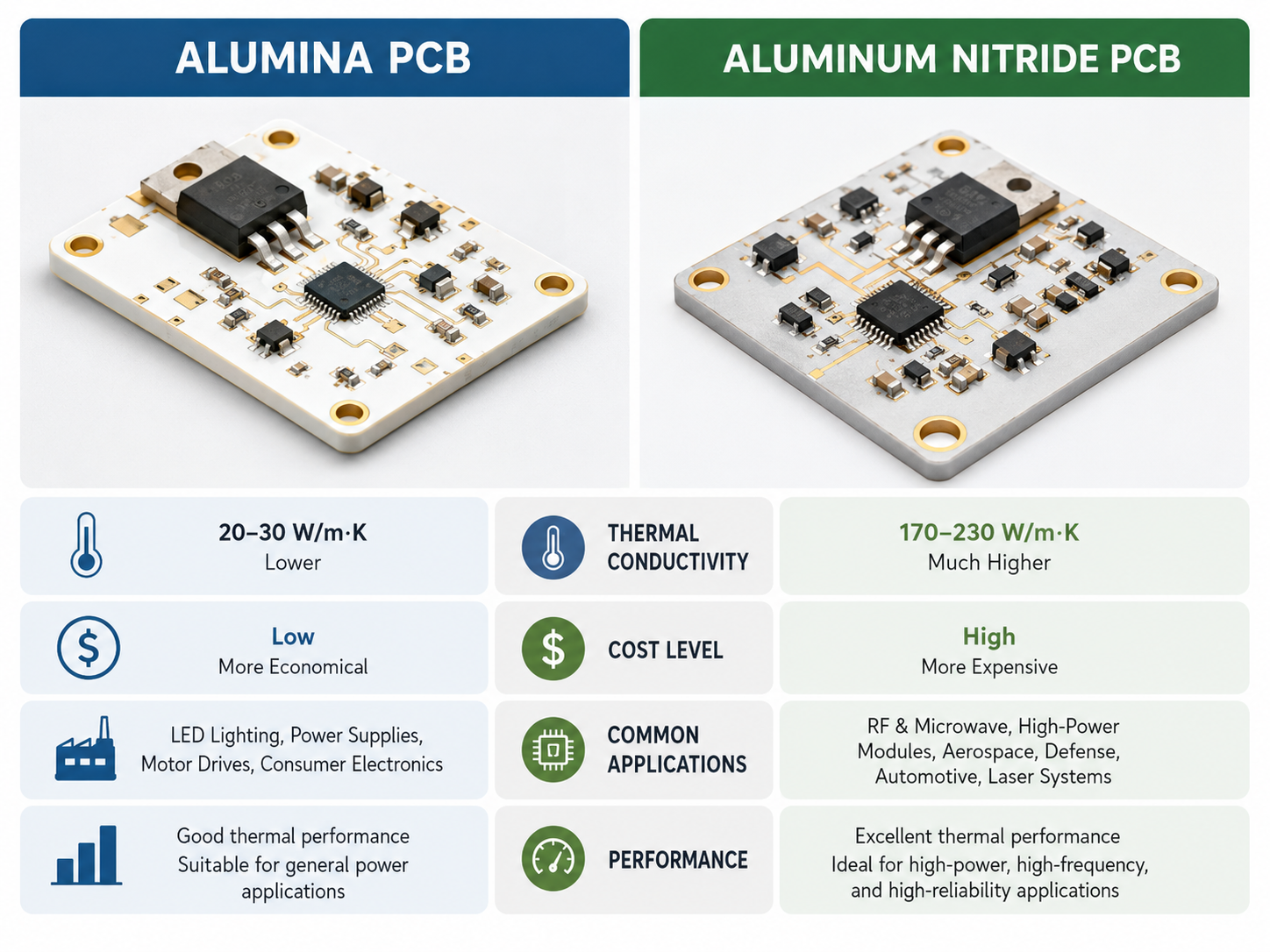
Typical FR4 has thermal conductivity of about 0.3 W/m·K. Alumina ceramic is commonly around 24–30 W/m·K, while aluminum nitride can reach about 140–180 W/m·K depending on grade and supplier.
EBest Circuit (Best Technology) supports ceramic PCB fabrication, component sourcing, SMT assembly, through-hole assembly, inspection, and testing. For ceramic projects, the engineering team usually reviews material selection, copper structure, component package, soldering method, and test requirements before production.
How Is Ceramic PCB Assembly Different from Standard PCB Assembly?
Ceramic PCB assembly follows many standard PCBA steps, but the process control is more specific. Standard FR4 boards have moderate flexibility and are easier to handle during panel processing, component insertion, and depaneling. Ceramic boards are dimensionally stable and thermally efficient, but they require more careful handling because the substrate is rigid and brittle.
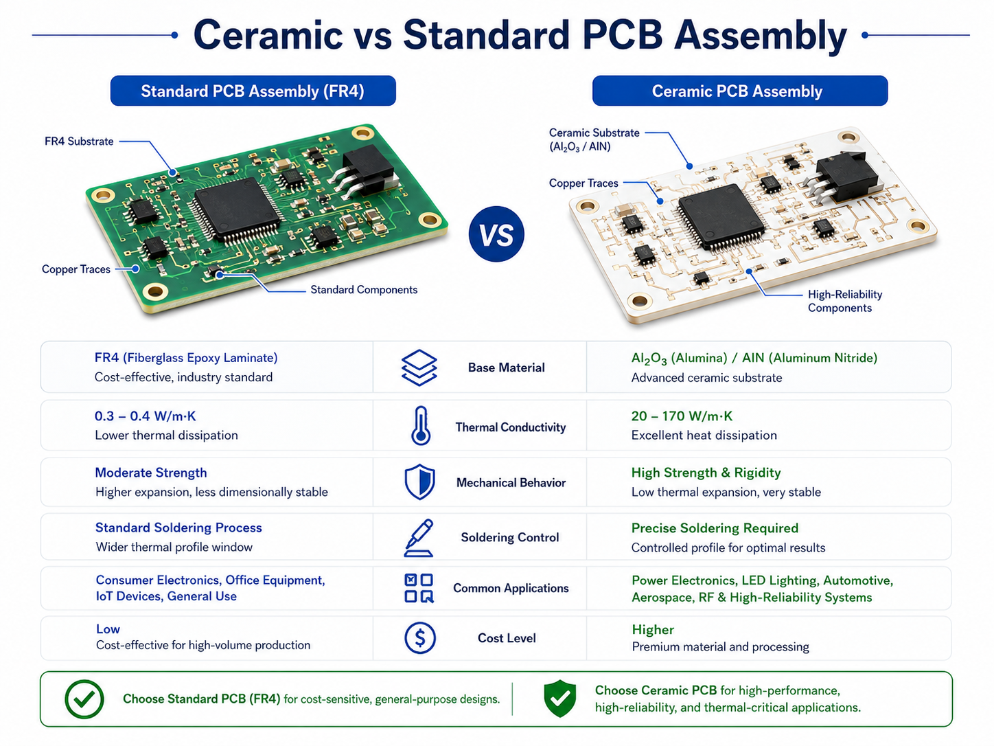
The copper structure can also be different. Ceramic boards may use DPC, DBC, AMB, thick-film, or thin-film technology. Each process has different copper thickness, line capability, bonding strength, and cost. For example, DBC is often used in power modules because it supports thicker copper and efficient thermal transfer. DPC is often used when fine lines and accurate metallization are required.
| Item | Standard FR4 PCB Assembly | Ceramic PCB Assembly |
|---|---|---|
| Base material | Glass fiber epoxy laminate | Alumina, aluminum nitride, silicon nitride, or other ceramic substrate |
| Thermal conductivity | Usually around 0.3 W/m·K | Commonly from 24 W/m·K to over 170 W/m·K |
| Mechanical behavior | More flexible | Rigid and requires careful handling |
| Soldering control | Wider process window | Requires more accurate thermal profiling |
| Copper structure | Standard etched copper layers | DPC, DBC, AMB, thick-film, or thin-film structures |
| Common applications | General electronics | Power, LED, RF, automotive, medical, aerospace, and industrial electronics |
| Cost level | Lower material and processing cost | Higher substrate, fabrication, and handling cost |
| Inspection focus | Placement, solder joints, polarity, electrical test | Solder joints, voids, cracks, copper adhesion, thermal pads, edge condition |
The main value of ceramic boards is performance under thermal, electrical, or mechanical demand. The main requirement is disciplined process control. When both are matched, ceramic assemblies can provide stable performance in applications where FR4 may not be suitable.
Can Through-Hole Components Be Used on Ceramic PCBs?
Through-hole components can be used on ceramic PCBs when the hole structure, lead size, soldering method, and mechanical stress are properly reviewed. Although many ceramic pcb boards use SMT components, some products still require pin headers, terminals, connectors, sensors, fuses, or power pins.
Hole formation in ceramic materials is different from FR4 processing. Depending on the material, board thickness, and hole diameter, holes may be made by laser drilling, mechanical drilling, or other ceramic-specific methods. If the hole needs electrical connection, the inner wall must be metallized. Hole tolerance, copper adhesion, and plating quality should be checked before production.
Through-hole assembly is often used in these ceramic PCB applications:
- Power modules with high-current pins or screw terminals.
- LED driver boards with power input and control connectors.
- Sensor modules requiring stable external wiring.
- High-voltage boards using leaded components with controlled spacing.
- Hybrid assemblies combining SMT parts and through-hole parts.
The soldering method depends on design and volume. Selective soldering, manual soldering, pin-in-paste reflow, or fixture-assisted soldering may be used. The process should control heat input and reduce mechanical force. For heavy components, mechanical support may be needed so the solder joints do not carry the full load during product use.
EBest Circuit (Best Technology) reviews through-hole ceramic designs by checking hole size, substrate thickness, copper structure, solder access, connector load, and inspection requirements.
What Files Are Needed for Ceramic PCB Assembly?
A complete file package helps the manufacturer quote, fabricate, assemble, and test the product correctly. For ceramic PCB assembly, the files should show not only the circuit layout but also the material, copper structure, component position, soldering notes, and test method.
For a ceramic pcb prototype, basic files may be enough for early quotation. For production, the documentation should be more complete, especially for power electronics, medical devices, automotive electronics, aerospace products, and industrial control modules.
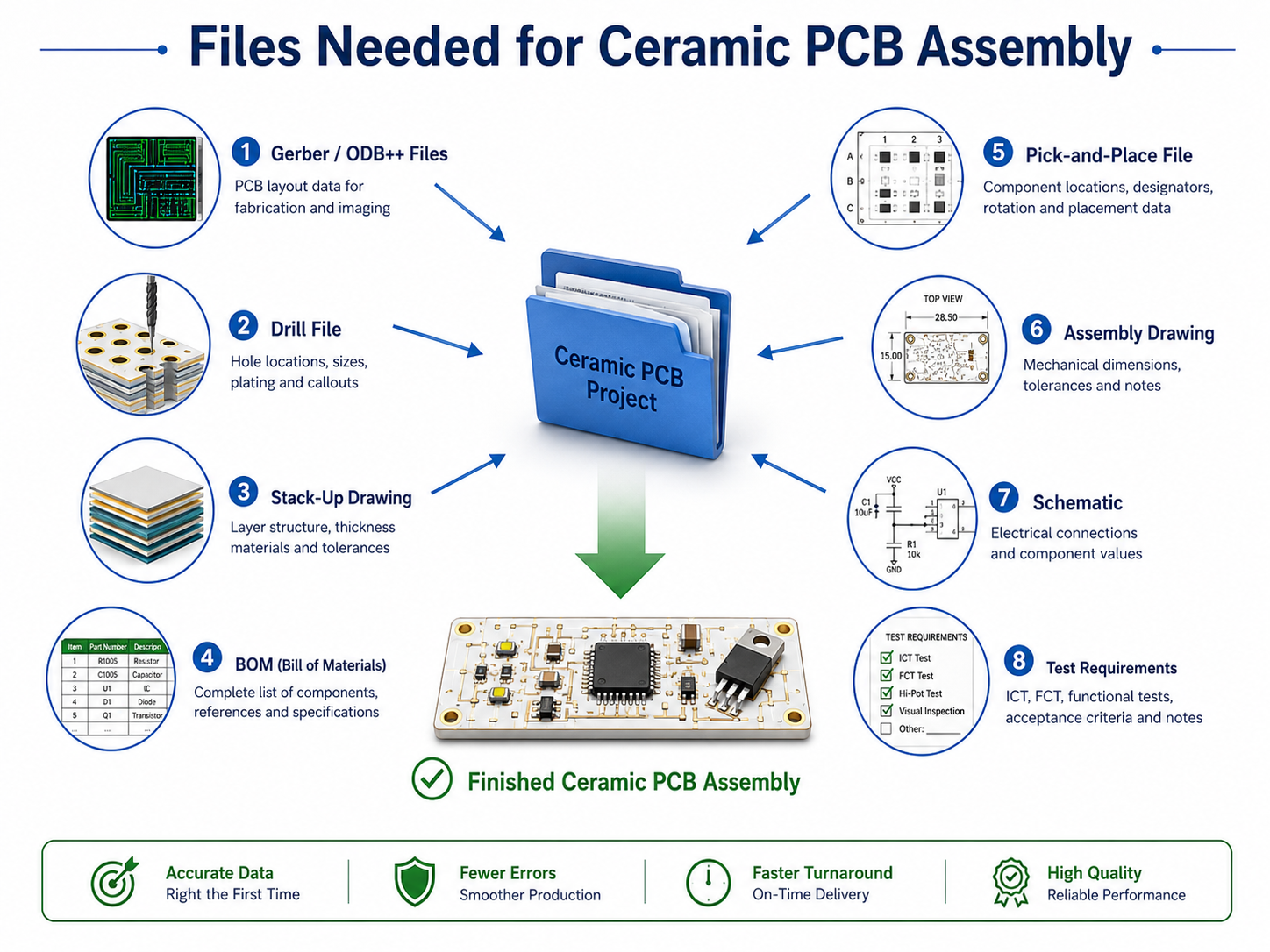
A practical file package usually includes:
- Gerber files or ODB++ files for PCB fabrication.
- Drill files for plated holes, non-plated holes, and slots.
- Stack-up drawing showing ceramic material, board thickness, copper thickness, and surface finish.
- BOM with manufacturer part number, package, quantity, tolerance, and approved alternatives.
- Pick-and-place file with coordinates and rotation.
- Assembly drawing showing polarity, orientation, special notes, and keep-out areas.
- Schematic for engineering review and test planning.
- Stencil requirements if solder paste aperture control is already defined.
- Test instructions for electrical test, functional test, programming, high-voltage test, or thermal test.
- Quality requirements such as IPC class, RoHS/REACH request, inspection criteria, and traceability level.
| File Type | Purpose | Why It Matters |
|---|---|---|
| Gerber or ODB++ | Defines circuit pattern | Confirms pad geometry, copper area, spacing, and fabrication data |
| Drill file | Defines holes and slots | Supports ceramic drilling and metallization review |
| Stack-up drawing | Defines material and thickness | Affects heat transfer, insulation, RF behavior, and mechanical strength |
| BOM | Defines components | Supports sourcing, assembly preparation, and alternative review |
| Pick-and-place file | Guides SMT placement | Reduces rotation and position errors |
| Assembly drawing | Shows component orientation and notes | Helps manual inspection and special process control |
| Schematic | Explains circuit function | Supports DFM review, testing, and troubleshooting |
| Test document | Defines acceptance method | Confirms how the finished assembly will be verified |
For ceramic pcb assembly service China projects, many overseas customers send partial information at the first RFQ stage. That is acceptable for budgetary review. Before production, the manufacturer should confirm all critical data.
EBest Circuit (Best Technology) can review the file package before production and provide feedback on manufacturability, BOM availability, component alternatives, and test planning.
What Should Be Checked Before Ceramic PCB Assembly?
Before assembly starts, the engineering team should confirm whether the design matches the selected ceramic material and production process. Ceramic boards are often used in high-value applications, so early checks can save time during prototype validation and batch production.
The first item is material selection. Alumina is widely used because it offers good insulation, stable performance, and controlled cost. Aluminum nitride is selected when heat dissipation is a major requirement. Silicon nitride is used in some demanding power and automotive applications because it offers good mechanical strength and thermal shock resistance.
The second item is copper structure. Copper thickness, line width, spacing, bonding method, and surface finish must match current load, heat transfer, insulation distance, and soldering requirements. For high-current circuits, thick copper may be required. For fine-pitch circuits, DPC or thin-film ceramic technology may be more suitable.
Pad design should also be reviewed. Large thermal pads can create solder voids if stencil openings are not optimized. Small pads may reduce solder joint strength or thermal transfer. For LEDs, QFN, LGA, MOSFETs, and power ICs, the stencil design, solder paste volume, and thermal pad layout should be checked together.
The BOM should be verified before SMT preparation. The review should cover package type, polarity, MSL level, lead time, lifecycle status, and substitute options.
Key pre-assembly checks include material grade, board thickness, copper thickness, surface finish, pad size, stencil aperture, component orientation, fixture design, handling method, reflow profile, cleaning requirement, test access, and traceability requirement. For high-voltage products, creepage and clearance should be reviewed. For RF products, impedance, dielectric constant, grounding structure, and connector transition should be checked.
EBest Circuit (Best Technology) provides DFM review for ceramic PCB and PCBA projects. The review focuses on practical production points, including material choice, soldering feasibility, component sourcing, inspection access, and testing method.
What Soldering Process Is Used for Ceramic PCB Assembly?
The soldering process depends on substrate material, copper structure, component type, board thickness, thermal mass, surface finish, and production volume. Most ceramic PCB assemblies use SMT reflow soldering for surface mount parts. Some products also require selective soldering, manual soldering, pin-in-paste reflow, vacuum reflow, or fixture-assisted soldering.
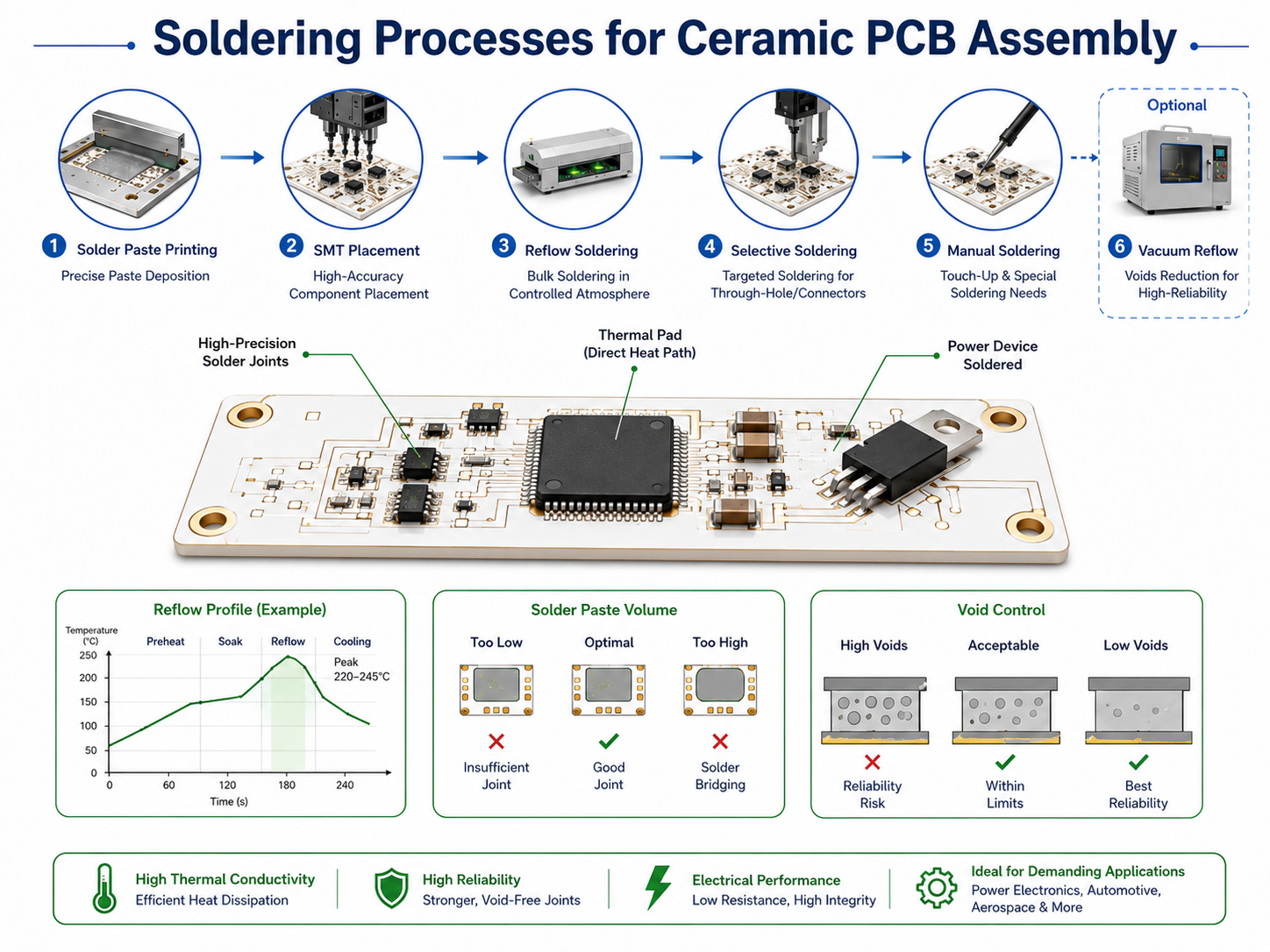
SMT reflow is used for LEDs, ICs, resistors, capacitors, sensors, RF parts, and many power devices. The process starts with solder paste printing. Components are then placed by SMT equipment, and the board passes through a controlled reflow oven.
| Soldering Method | Typical Use | Key Control Point |
|---|---|---|
| SMT reflow soldering | LEDs, ICs, resistors, capacitors, sensors, RF parts | Reflow profile, solder paste volume, thermal balance |
| Selective soldering | Through-hole connectors, terminals, and pins | Local heating, hole fill, substrate stress |
| Manual soldering | Prototype, low-volume, special components | Tip temperature, contact time, operator consistency |
| Pin-in-paste reflow | Through-hole pins assembled during SMT | Paste volume, lead length, hole fill |
| Vacuum reflow | Power modules and large thermal pads | Void reduction under hidden pads |
| Fixture-assisted soldering | Special structures or heavy components | Alignment, stability, and heat uniformity |
Solder paste selection should match surface finish, component terminal plating, and reliability requirements. Lead-free SAC solder is common, while high-temperature solder or special alloys may be used for certain power or harsh-environment applications. Flux residue requirements should also be confirmed, especially for high-voltage, RF, medical, and clean electronic assemblies.
How Are Ceramic PCB Assemblies Tested?
Ceramic PCB assemblies are tested through visual inspection, AOI, X-ray inspection, electrical test, functional test, and application-specific verification. The test plan depends on circuit function, product risk, industry requirement, and customer acceptance criteria.
Visual inspection checks ceramic edges, surface condition, component placement, solder appearance, polarity, marking, contamination, and mechanical damage. Since ceramic substrates are rigid, edge chips and cracks should be checked carefully.
AOI is used after SMT reflow to check missing parts, wrong parts, offset, polarity, tombstoning, solder bridges, and visible solder issues. AOI is efficient for visible components, but it cannot inspect hidden solder joints under BGA, QFN, LGA, or large thermal pads.
X-ray inspection is useful for hidden joints and large thermal pads. It helps identify solder voids, bridging, insufficient solder, and alignment problems.
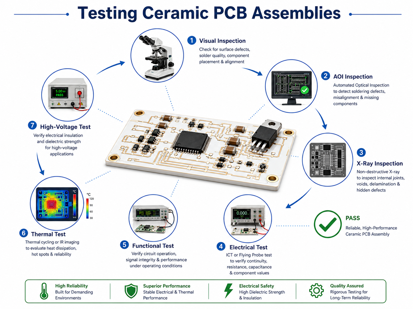
Electrical testing confirms continuity, isolation, and circuit behavior. Depending on the design, the test may include open/short test, insulation resistance test, high-voltage test, current test, programming, communication check, or full functional test. RF ceramic boards may require impedance-related checks, return loss, insertion loss, or frequency response testing based on product requirements.
| Test Method | What It Checks | Typical Use |
|---|---|---|
| Visual inspection | Surface condition, solder appearance, ceramic edges, polarity | First-level quality control |
| AOI | Placement, missing parts, solder bridges, polarity | SMT process verification |
| X-ray | Hidden joints, voids, BGA/QFN/LGA soldering | Power, LED, and fine-pitch assemblies |
| Electrical test | Opens, shorts, isolation, basic circuit integrity | Bare board and assembled board verification |
| Functional test | Product operation under defined conditions | Production acceptance |
| Thermal test | Temperature rise and heat path behavior | LED, power, and high-current products |
| High-voltage test | Insulation and safety spacing | Power and high-voltage circuits |
| Aging or burn-in | Stability over time and temperature | Higher-reliability applications |
EBest Circuit (Best Technology) supports AOI, X-ray, electrical test, functional test, and project-based traceability for ceramic PCB and PCBA projects.
What Common Problems Can Happen During Ceramic PCB Assembly?
Ceramic PCB assembly is reliable when design, material, and process are aligned. Most process issues are linked to material handling, soldering profile, pad design, documentation, or component stress. Early DFM review and controlled production methods can reduce these risks.
| Possible Issue | Main Cause | Control Method |
|---|---|---|
| Edge chipping | Handling impact, unsuitable fixture, rough tooling | Use protective packaging and controlled fixtures |
| Substrate cracking | Mechanical stress or rapid thermal change | Review mounting, insertion force, and reflow profile |
| Solder voids | Large thermal pads or unsuitable paste/profile | Optimize stencil, paste, reflow, and X-ray control |
| Poor wetting | Surface contamination or finish mismatch | Control storage and verify solderability |
| Tombstoning | Pad imbalance or uneven heating | Review pad design, paste volume, and profile |
| Component shift | Excess paste, vibration, package imbalance | Improve placement and reflow stability |
| Limited test coverage | Missing test points or unclear procedure | Define test access and acceptance limits early |
The practical solution is to review fabrication, assembly, component sourcing, and testing together. A qualified ceramic pcb manufacturer should identify process risks before production and provide clear recommendations for improvement.
What Affects Ceramic PCB Assembly Cost?
Ceramic PCB assembly cost is affected by material, board size, board thickness, copper thickness, metallization method, surface finish, component selection, assembly complexity, test scope, order quantity, and lead time. A ceramic board price is usually higher than FR4 because ceramic materials, fabrication processes, and handling requirements are different.
Material choice is a major factor. Alumina is usually more economical and widely used. Aluminum nitride costs more but provides much higher thermal conductivity. Silicon nitride and other advanced ceramic materials may be selected for mechanical strength, thermal shock resistance, or special operating conditions.
Fabrication method also affects cost. DPC, DBC, AMB, thick-film, and thin-film ceramic processes have different production requirements. Fine lines, tight spacing, thick copper, large copper coverage, and special surface finishes increase process complexity.
Assembly cost depends on component count, package type, placement density, soldering method, and inspection level. Fine-pitch ICs, QFN, BGA, high-power packages, large thermal pads, and through-hole terminals require more process control. X-ray inspection, functional testing, high-voltage testing, thermal testing, programming, conformal coating, and serialization also affect the final cost.
A ceramic pcb prototype usually has a higher unit price because setup, stencil, engineering review, tooling, and process preparation are spread across a small quantity. After the design is verified, batch production can reduce unit cost through better material planning and repeatable process flow.
EBest Circuit (Best Technology) can review stack-up, BOM, assembly method, and test scope during quotation, helping customers understand the main cost drivers before production.
Why Choose China Ceramic PCB Assembly?
China ceramic PCB assembly is widely used by global electronics companies because it combines PCB fabrication, component sourcing, SMT assembly, testing, and production scaling in one mature supply chain.
A capable China ceramic PCB assembly partner can support LED modules, power electronics, industrial controls, RF devices, medical electronics, automotive assemblies, and high-temperature products.
Component sourcing is also important. Many ceramic PCB projects use LEDs, power semiconductors, RF parts, connectors, sensors, passives, and thermal materials. A supplier with sourcing capability can check lead time, lifecycle status, approved alternatives, and package compatibility before assembly.
When choosing ceramic pcb assembly service china, buyers should evaluate capability, not only price. The supplier should understand ceramic materials, copper structure, soldering control, void inspection, through-hole processing, functional testing, and English technical communication.
EBest Circuit (Best Technology) provides ceramic PCB fabrication, component sourcing, SMT assembly, through-hole assembly, testing, and engineering support. For ceramic projects, the team can review material selection, manufacturability, BOM status, soldering method, inspection requirements, and delivery schedule.tion.
If you are looking for a ceramic PCB manufacturer or need support for ceramic PCB assembly in China, send your drawings, BOM, and project requirements to sales@bestpcbs.com for review and quotation.