PCB manufacturing PCB manufacturing
Home > Blog

aluminum nitride pcb

Ceramic Core PCB | Alumina & Aluminum Nitride Ceramic PCB
Monday, May 11th, 2026

What is a ceramic core PCB?

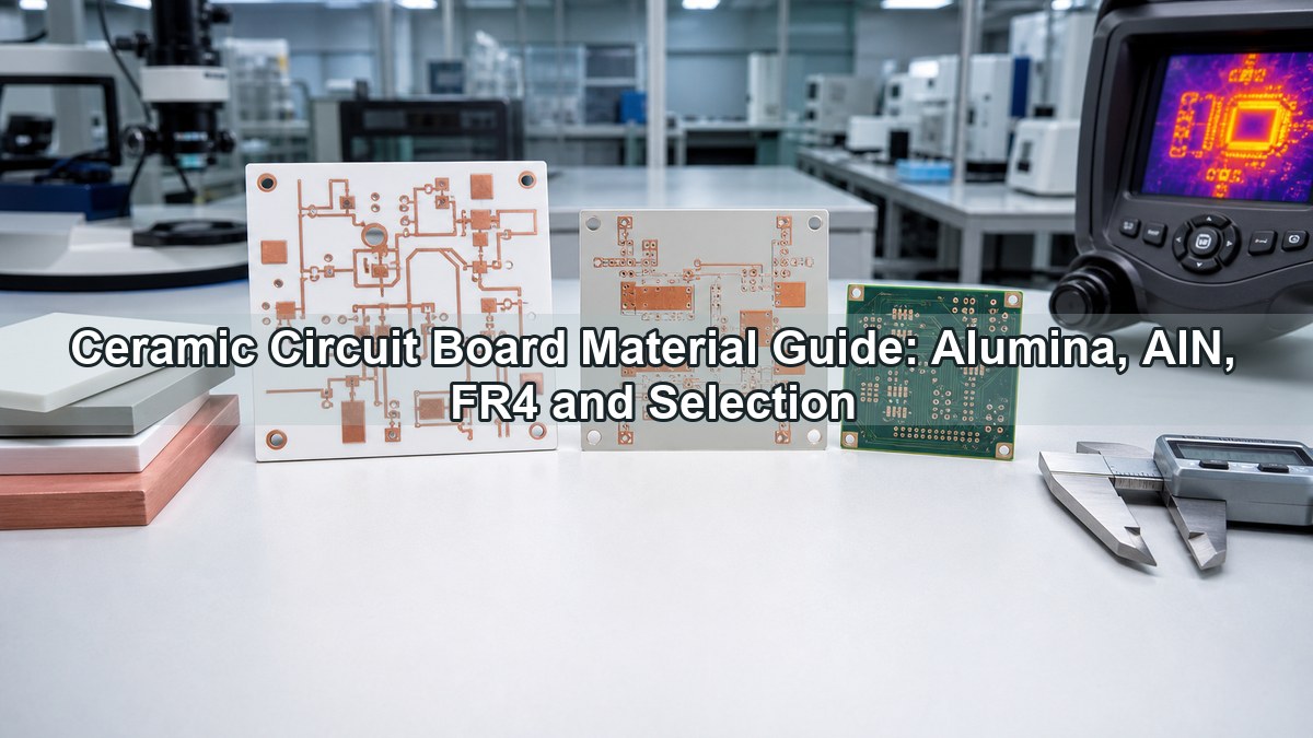
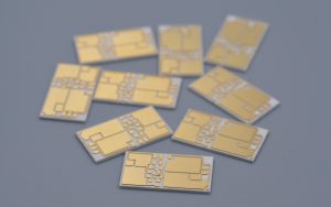
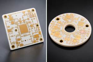
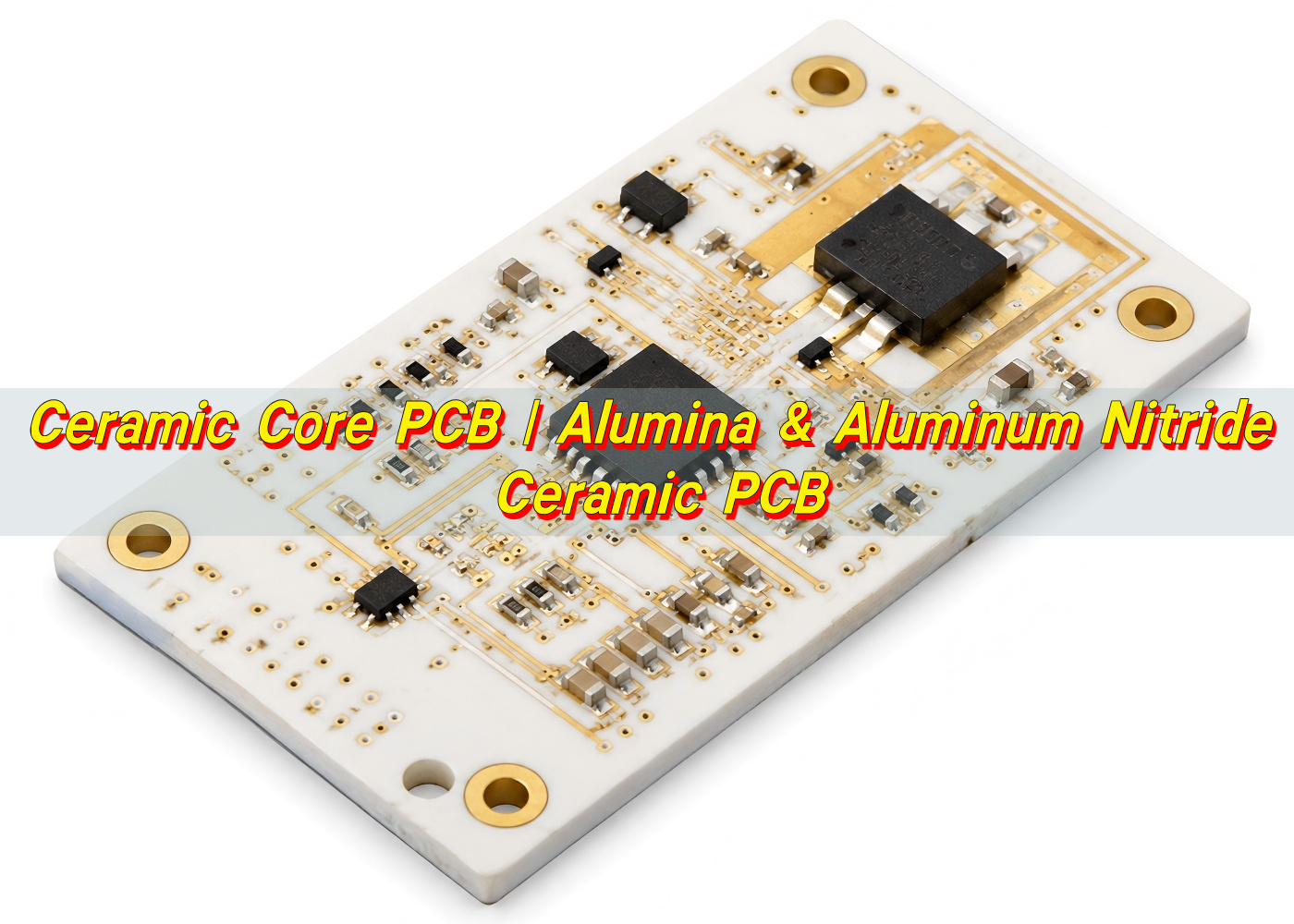
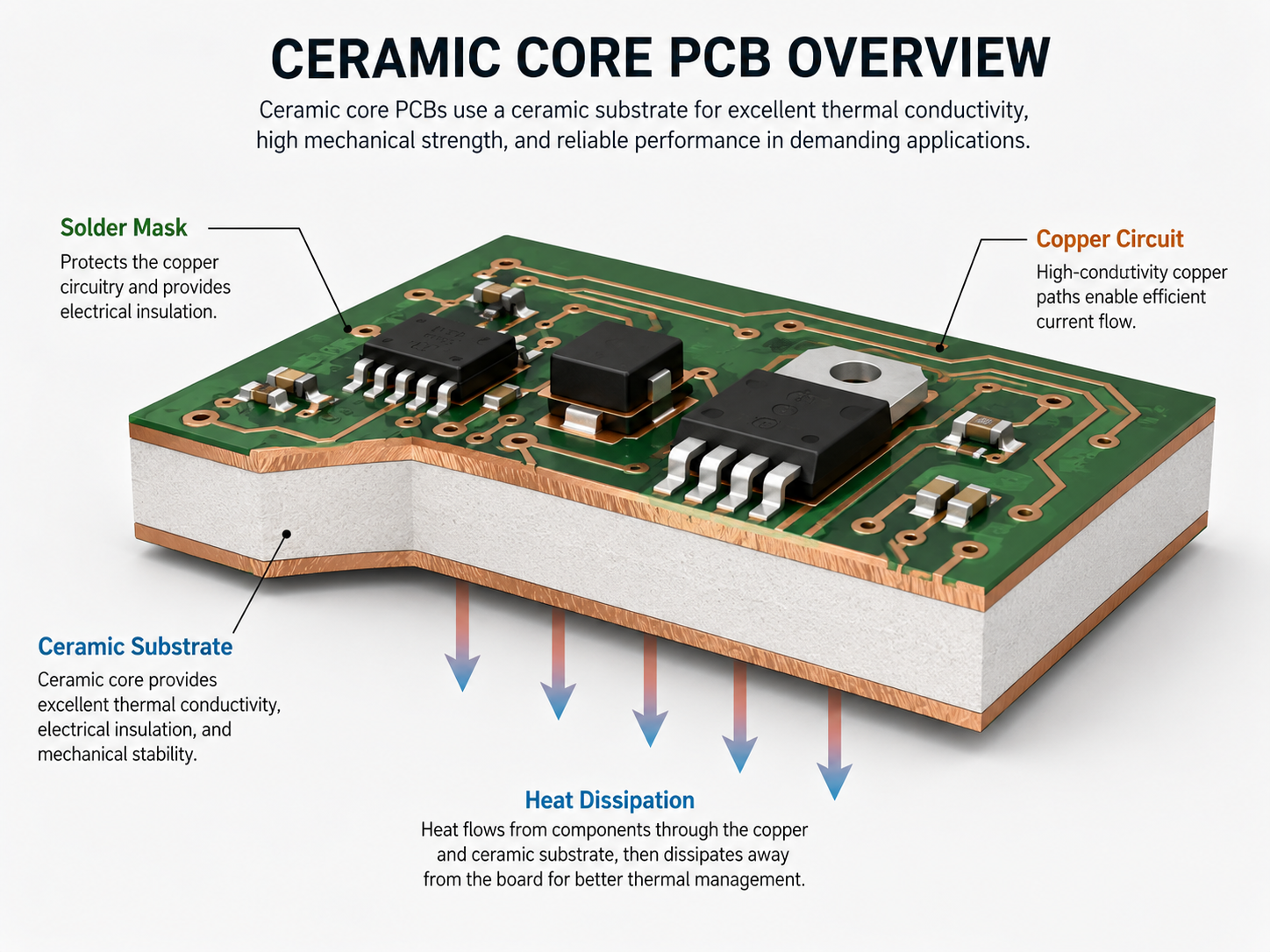
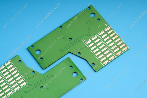
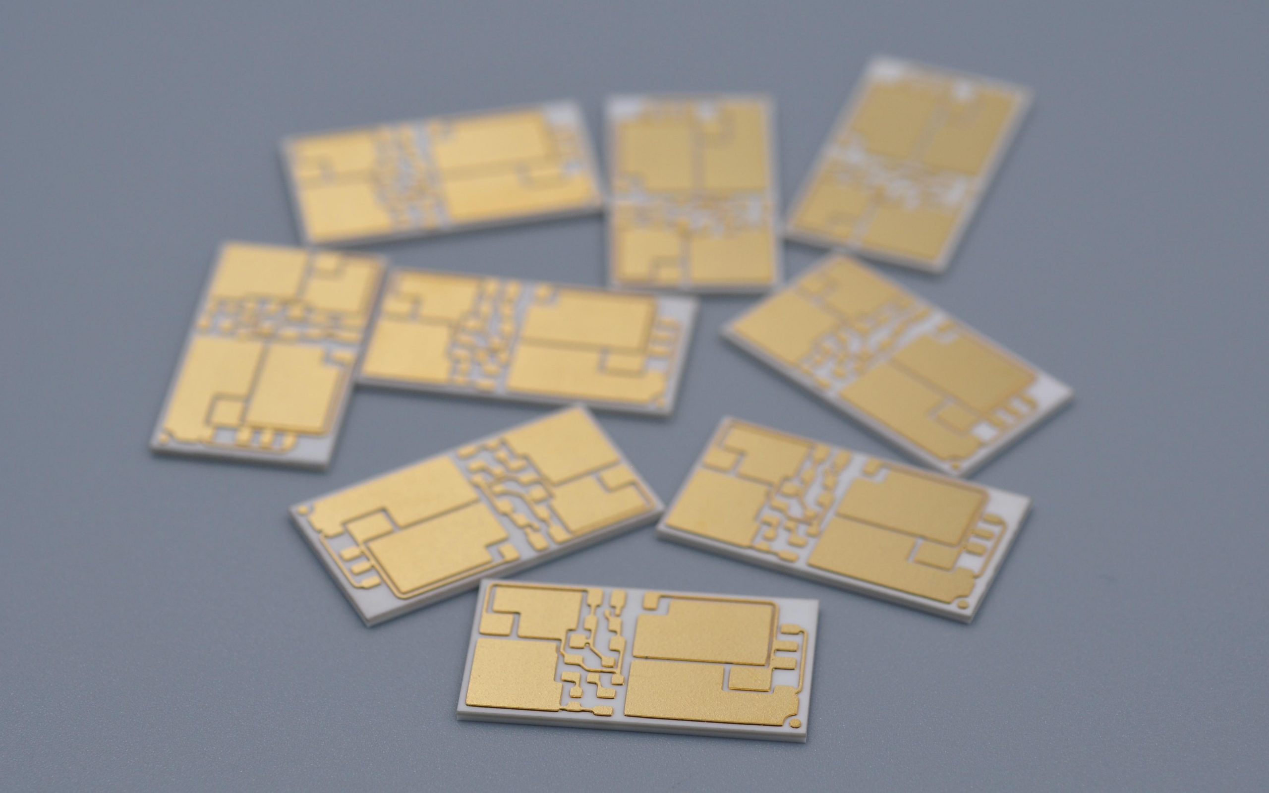
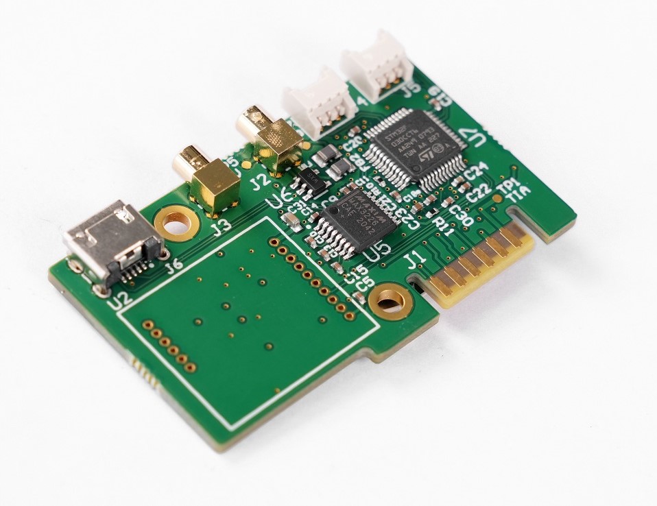
Ceramic core PCB is a printed circuit board built on a ceramic substrate instead of a conventional organic laminate such as FR4. In this type of board, the ceramic layer works as the main supporting base and thermal pathway. It gives the circuit strong heat transfer, stable electrical insulation, and excellent dimensional consistency under demanding operating conditions.

Unlike standard PCB materials that rely on glass fiber and resin, ceramic PCB boards use inorganic ceramic materials such as alumina, aluminum nitride, or silicon nitride. These materials are valued in high-power, high-frequency, high-temperature, and high-reliability electronics.

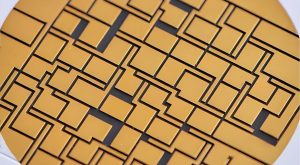
In the PCB industry, ceramic core PCB is often used for applications where ordinary laminates cannot provide enough thermal conductivity or long-term stability. The board may support thick copper, thin-film circuits, DPC copper plating, DBC bonding, or AMB structures, depending on the electrical and mechanical requirements of the project.

EBest Circuit (Best Technology) supports ceramic PCB manufacturing for engineers who need more than a basic circuit board. With experience in alumina PCB, aluminum nitride PCB, DPC ceramic PCB, DBC ceramic substrate, AMB ceramic substrate, and customized ceramic PCB boards, EBest Circuit helps customers move from early design review to production with practical engineering support.

What is the difference between ceramic and FR4?

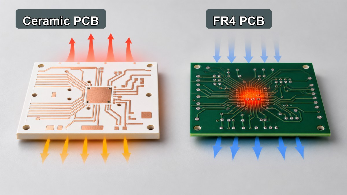
Ceramic PCB and FR4 PCB are both widely used in electronics, but they are designed for different performance levels. FR4 is the most common PCB substrate because it is cost-effective, easy to process, and suitable for many consumer, industrial, and general electronic products. Ceramic PCB is selected when the circuit needs higher thermal conductivity, better temperature resistance, and stronger dimensional stability.

FR4 is made from woven fiberglass cloth and epoxy resin. It performs well in standard electronic assemblies, but its thermal conductivity is limited. Ceramic boards, by contrast, use inorganic ceramic substrates that conduct heat much more efficiently while keeping excellent insulation. This is why ceramic core PCB is commonly found in LED modules, laser equipment, power electronics, sensors, medical devices, automotive electronics, and aerospace-related systems.

ItemCeramic Core PCBFR4 PCB
Main materialAlumina, aluminum nitride, silicon nitride, or other ceramic materialsGlass fiber reinforced epoxy laminate
Thermal conductivityHigh, suitable for heat-sensitive and power applicationsLow to moderate, suitable for general electronics
Temperature resistanceExcellent stability at elevated temperaturesGood for standard operating environments
Mechanical behaviorHard, stable, and rigid, but requires careful handlingTougher and more flexible during standard assembly
Electrical insulationVery strong insulation performanceReliable insulation for common circuit designs
Typical applicationsHigh-power LEDs, RF modules, power devices, sensors, automotive electronicsConsumer electronics, control boards, communication devices, general PCBA
Cost levelHigher due to material and process complexityLower and highly scalable

The choice should not be based only on price. If the circuit generates a high amount of heat or must keep stable performance in a harsh environment, ceramic PCB can provide a stronger technical foundation.

What’s the difference between alumina PCB and aluminum nitride PCB?

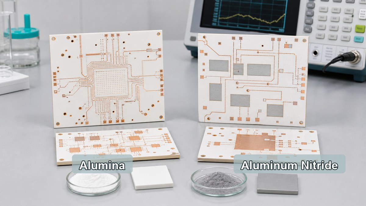
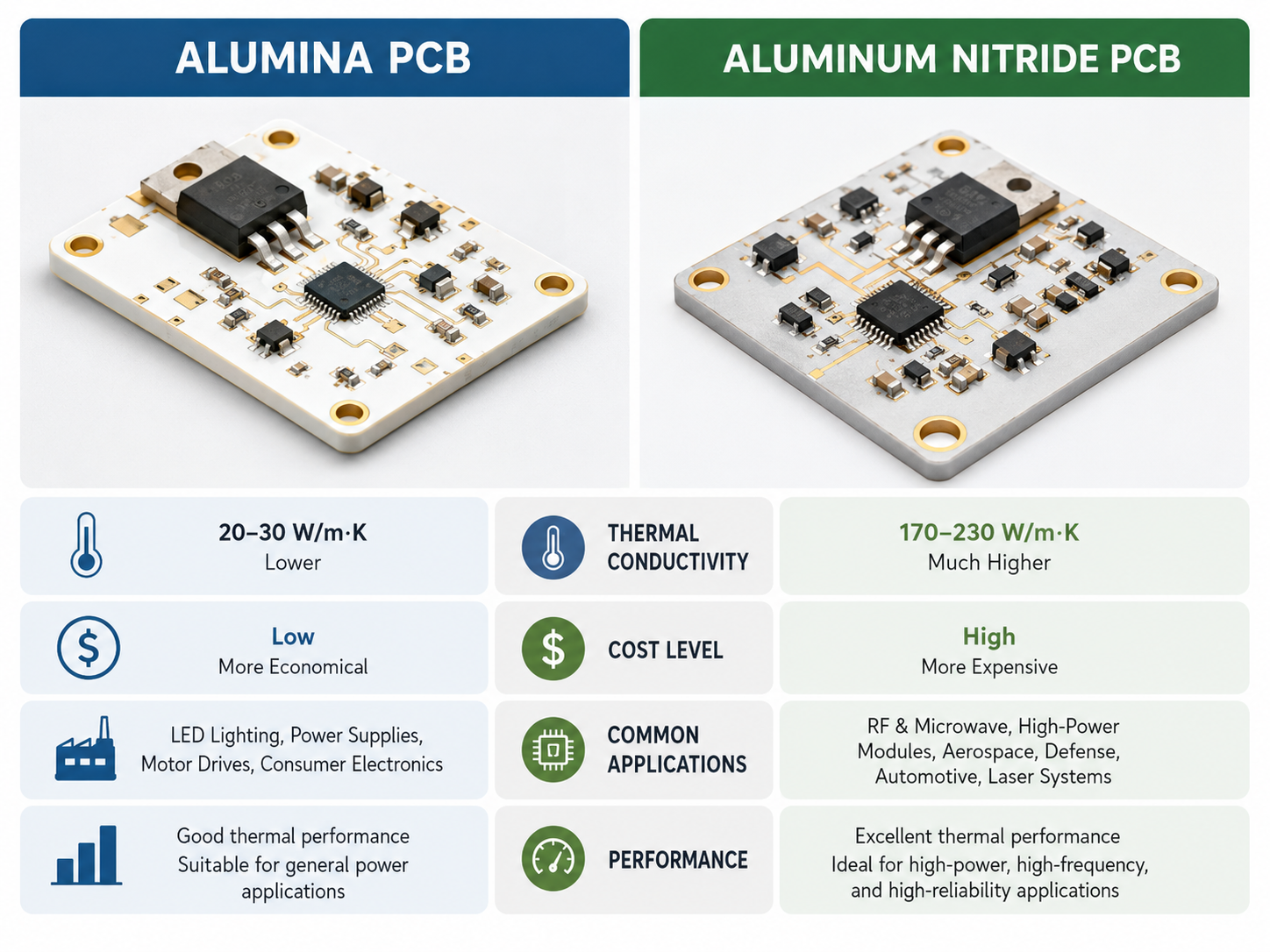
Alumina PCB and aluminum nitride PCB are two of the most common ceramic PCB materials. Both provide good insulation, stable structure, and better thermal performance than FR4. The key difference is thermal conductivity. Alumina is widely used because it offers a balanced combination of price, process maturity, and electrical performance. Aluminum nitride is chosen when the design needs much higher heat dissipation.

Alumina PCB usually refers to ceramic boards made from aluminum oxide. Common grades include 96% alumina and 99.6% alumina. It is a practical choice for many LED, sensor, power module, and industrial electronic applications. It has good mechanical strength, stable electrical insulation, and a more accessible ceramic board price compared with aluminum nitride.

Aluminum nitride PCB is often used in more demanding thermal designs. Its thermal conductivity can be several times higher than alumina, making it highly suitable for power semiconductors, high-brightness LEDs, laser diodes, automotive power modules, and compact high-power assemblies. It is usually more expensive than alumina because the raw material, sintering process, and manufacturing control are more demanding.

ItemAlumina PCBAluminum Nitride PCB
MaterialAluminum oxide ceramicAluminum nitride ceramic
Thermal conductivityGood, commonly used for medium to high thermal needsExcellent, suitable for high-power heat dissipation
CostMore economical among ceramic PCB optionsHigher due to material and process requirements
Mechanical strengthStrong and mature in productionStrong, with careful process control needed
Electrical insulationExcellentExcellent
Typical useLED modules, sensors, heaters, industrial controls, power circuitsPower modules, laser devices, high-power LEDs, RF and automotive electronics

EBest Circuit can help customers compare ceramic PCB materials during DFM review, so the final design matches both technical needs and production cost targets.

Why use ceramic PCB?

Ceramic PCB is used because it solves several practical engineering problems at the same time. It helps remove heat, keeps circuits electrically insulated, supports high-density layouts, and performs well in high-temperature environments.

One of the strongest reasons to use ceramic PCB is thermal management. As electronic products become smaller and more powerful, heat has less room to escape. If heat remains around chips, LEDs, or power components, performance can drop over time. A ceramic board gives heat a faster path away from the source, helping the assembly work in a more stable condition.

Ceramic PCB also supports excellent electrical properties. It can provide low dielectric loss, high insulation resistance, and stable performance across demanding operating conditions. This is important for RF circuits, sensor modules, high-voltage electronics, and power devices.

  • High thermal conductivity for better heat spreading
  • Strong electrical insulation for compact circuit layouts
  • Excellent temperature resistance for harsh environments
  • Stable dimensions during thermal cycling
  • Good compatibility with power devices, LEDs, sensors, and RF modules
  • Long service life in high-reliability electronic products

For manufacturers, ceramic PCB also brings value in quality consistency. The substrate has stable physical properties, which helps reduce performance drift in precision electronics. For engineers, it allows a cleaner thermal design and can reduce the need for bulky heat sinks in some compact products.

How much does a ceramic PCB cost?

Ceramic PCB cost is usually higher than standard FR4 PCB cost because the material, processing method, copper bonding, laser drilling, metallization, and quality control are more specialized. In high-power or high-reliability products, better heat transfer and longer operating stability can reduce the risk of field problems and improve product performance.

The ceramic board price depends on several technical factors. Material selection is one of the biggest cost drivers. Alumina PCB is generally more economical, while aluminum nitride PCB costs more because it provides much higher thermal conductivity. Board size, thickness, copper thickness, circuit precision, via structure, surface finish, tolerance control, and production quantity also affect the final quotation.

Cost FactorHow It Affects Ceramic PCB Cost
Ceramic materialAlumina is usually more economical; aluminum nitride is higher in cost but stronger in thermal performance.
Board sizeLarger ceramic boards use more raw material and may require tighter handling control.
Substrate thicknessSpecial thickness requirements may increase material preparation and processing cost.
Copper thicknessThicker copper improves current capacity but increases plating or bonding complexity.
Line width and spacingFine circuits require more precise manufacturing control.
Via structureFilled vias, laser vias, and conductive vias can raise process complexity.
Surface finishENIG, immersion silver, nickel gold, or other finishes may affect pricing.
Order quantityPrototype cost per piece is higher; batch production usually improves unit cost.

For a reliable ceramic PCB quotation, engineers should provide Gerber files, drawings, material requirements, board thickness, copper thickness, surface finish, tolerance needs, and expected quantity. If the design is still being evaluated, EBest Circuit can review the technical requirements and suggest a practical manufacturing route before final pricing.

Can ceramic core PCB be customized in size and layout?

Yes, ceramic core PCB can be customized in size, layout, thickness, copper pattern, surface finish, and structure. Customization is one of the main reasons ceramic PCB is used in advanced electronic products.

Custom ceramic PCB does require careful design planning. Ceramic materials are hard and stable, but they are processed differently from FR4. Features such as hole size, edge shape, slot position, via design, copper thickness, and board outline should be reviewed before production. A strong DFM check helps improve manufacturability and keeps the finished board aligned with the original electrical and thermal goals.

Common customization options include:

  • Alumina PCB or aluminum nitride PCB substrate selection
  • Custom board outline, size, and ceramic thickness
  • Single-sided, double-sided, or multilayer ceramic PCB structure
  • Thin-film or thick-film circuit design
  • DPC, DBC, or AMB ceramic core manufacturing process
  • ENIG, nickel gold, silver, or other surface finish options
  • Laser drilling, via filling, and precision routing
  • Thick copper design for higher current carrying capacity

EBest Circuit works with customers on customized ceramic PCB projects where standard PCB materials may not deliver enough thermal or mechanical stability. The engineering team can assist with material selection, stack-up review, ceramic core manufacturing process evaluation, and production feasibility checks.

How are ceramic cores made?

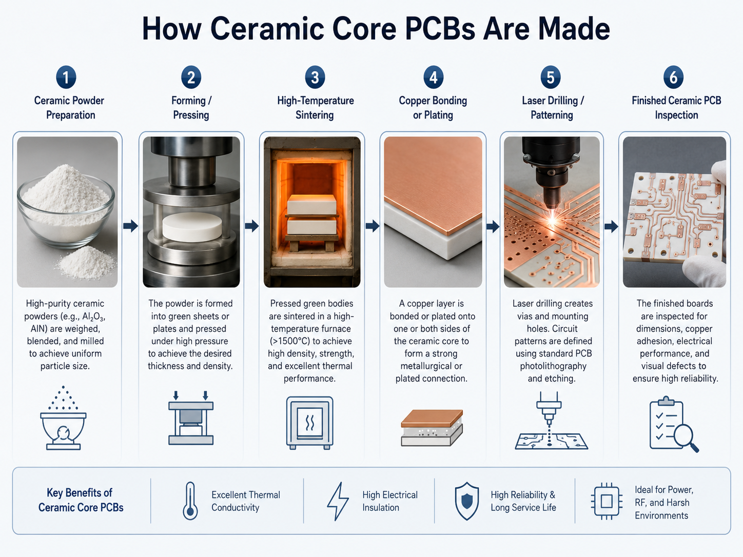
Ceramic cores are made through a controlled process that starts with ceramic powder preparation and ends with a dense, stable substrate suitable for circuit formation. The exact process depends on the material and final PCB structure.

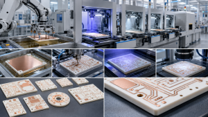
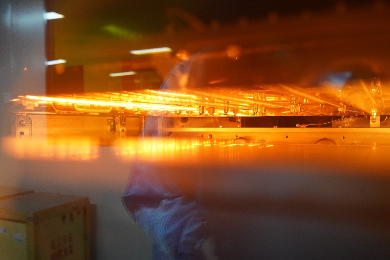
In a typical ceramic substrate process, ceramic powder is mixed with binders and additives to form a workable material. The material is shaped into sheets or pressed forms, then dried and sintered at high temperature. Sintering gives the ceramic its hardness, density, and stable physical properties. After that, the substrate may be lapped, polished, laser drilled, metallized, plated, etched, and finished according to the PCB design.

For circuit formation, different ceramic PCB technologies can be used. DPC, or Direct Plated Copper, is often chosen for fine circuits and high-precision designs. DBC, or Direct Bonded Copper, bonds copper directly onto the ceramic surface and is often used for power modules. AMB, or Active Metal Brazing, provides very strong bonding and is suitable for high-reliability power electronics.

Process TypeMain FeatureTypical Application
DPC ceramic PCBUses copper plating technology for fine circuits and precision patternsLED modules, sensors, optical devices, high-density ceramic circuits
DBC ceramic PCBDirect copper bonding provides strong thermal and current capacityPower modules, IGBT substrates, high-power electronics
AMB ceramic PCBActive brazing creates strong copper-to-ceramic bondingAutomotive power modules, high-reliability energy electronics
Thick-film ceramic PCBConductive paste is printed and fired onto ceramicHeaters, sensors, hybrid circuits, industrial modules
Thin-film ceramic PCBHigh-precision metal layers are deposited on ceramicMicrowave circuits, precision sensors, RF electronics

A professional ceramic PCB manufacturer must control material quality, sintering conditions, copper adhesion, surface flatness, circuit accuracy, and inspection standards. EBest Circuit combines process knowledge with practical PCB engineering support, helping customers choose the right ceramic core manufacturing process for the final product environment.

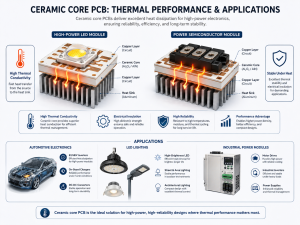
What thermal performance does ceramic core PCB deliver?

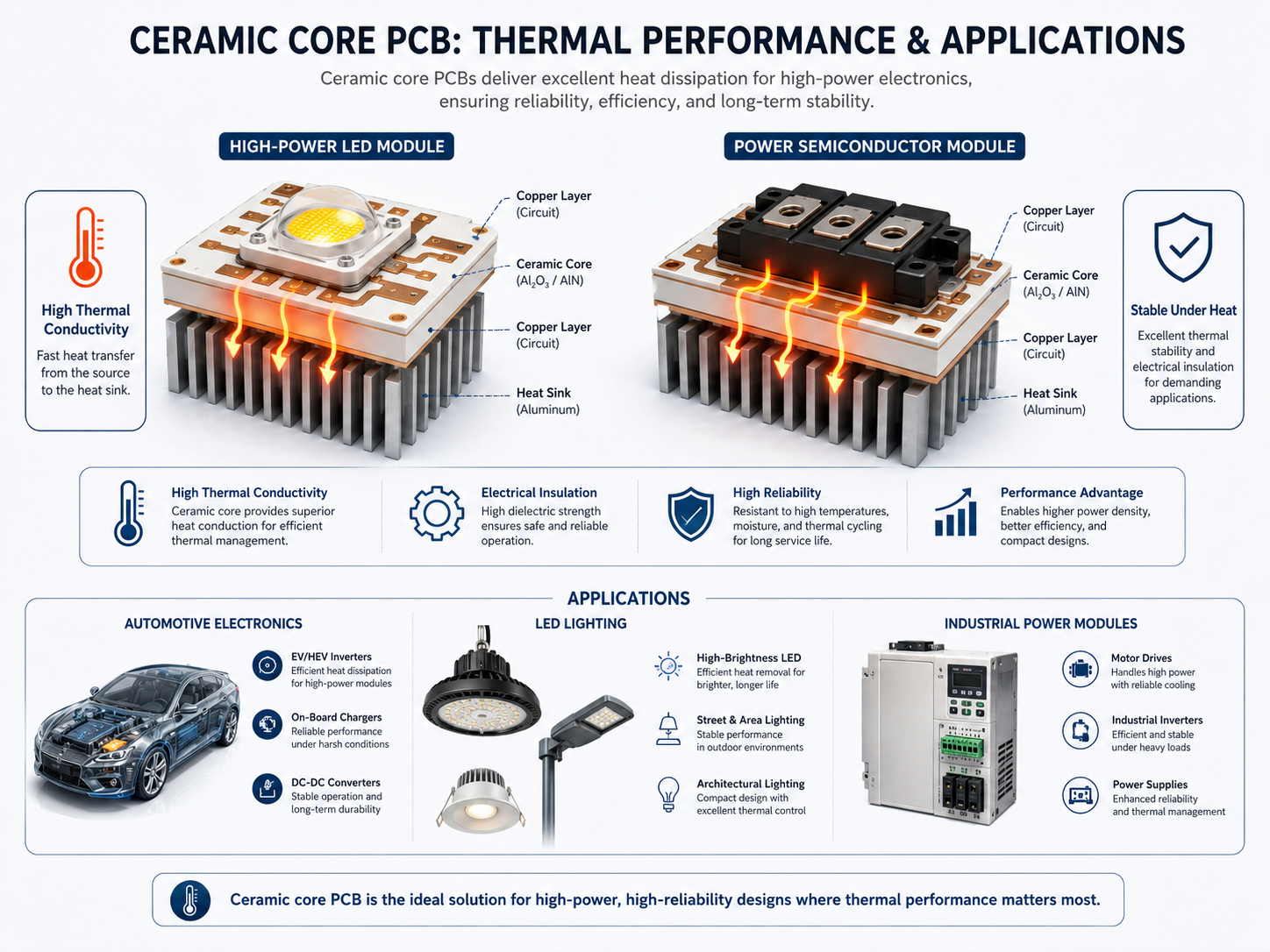
Ceramic core PCB delivers much stronger thermal performance than standard FR4 boards. The main advantage is that ceramic materials can transfer heat efficiently while still providing electrical insulation.

Alumina PCB offers good thermal conductivity for many industrial and LED applications. Aluminum nitride PCB provides a much higher level of heat transfer and is often used where thermal density is more demanding. With the right copper thickness, layout, and mounting structure, ceramic PCB boards can move heat away from components quickly and help maintain stable operating temperatures.

Thermal performance is not only about the ceramic material itself. The final result also depends on copper design, substrate thickness, dielectric path, via structure, solder joint quality, component placement, and heat sink contact.

MaterialGeneral Thermal PerformanceBest-Fit Applications
FR4Limited thermal conductivityGeneral electronics and low-to-medium power circuits
Alumina ceramicGood thermal conductivity with balanced costLEDs, sensors, industrial modules, moderate power electronics
Aluminum nitride ceramicExcellent thermal conductivityHigh-power LEDs, laser modules, power semiconductors, automotive electronics
Silicon nitride ceramicStrong thermal and mechanical reliabilityHigh-reliability power modules and harsh operating environments

For thermal-sensitive designs, EBest Circuit can support layout review and material comparison. This is helpful when customers need to decide between alumina PCB and aluminum nitride PCB, or when they want to optimize the balance between ceramic PCB cost, heat dissipation, and long-term reliability.

What are ceramic cores used for?

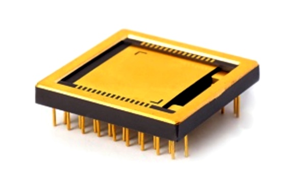
Ceramic cores are used in electronic products that need better thermal control, high insulation, stable structure, and reliable performance under demanding conditions. They are especially useful where compact size and high power must coexist. Because ceramic materials can transfer heat efficiently while maintaining electrical separation, they are widely used in modern power, lighting, automotive, medical, and communication systems.

In LED products, ceramic PCB helps move heat away from LED chips and supports stable brightness. In power electronics, ceramic substrates are used for modules that handle high current and high voltage. In RF and microwave circuits, ceramic materials can provide stable electrical characteristics. In medical and aerospace electronics, ceramic PCB boards support reliability, precision, and long service life.

  • High-power LED modules and lighting engines
  • Laser diode modules and optical devices
  • Power semiconductor packages and IGBT modules
  • Automotive electronics and electric vehicle power modules
  • RF, microwave, and communication circuits
  • Medical sensors and monitoring devices
  • Industrial control modules and high-temperature electronics
  • Aerospace, UAV, and high-reliability electronic assemblies

Ceramic core PCB is a strong choice when the product needs more than ordinary PCB performance. Alumina PCB is suitable for balanced thermal and cost requirements, while aluminum nitride PCB is ideal for stronger heat dissipation. For custom ceramic PCB boards, ceramic PCB materials, ceramic PCB cost evaluation, and ceramic core manufacturing process support, EBest Circuit (Best Technology) can help engineers build a practical path from prototype to production.

Summary:

Ceramic core PCB is not simply a premium version of FR4. It is a specialized circuit platform for products that need excellent heat transfer, high insulation, stable operation, and compact design. If your project requires alumina PCB, aluminum nitride PCB, or custom ceramic PCB manufacturing support, you can contact sales@bestpcbs.com for project discussion and quotation support.

You may also like

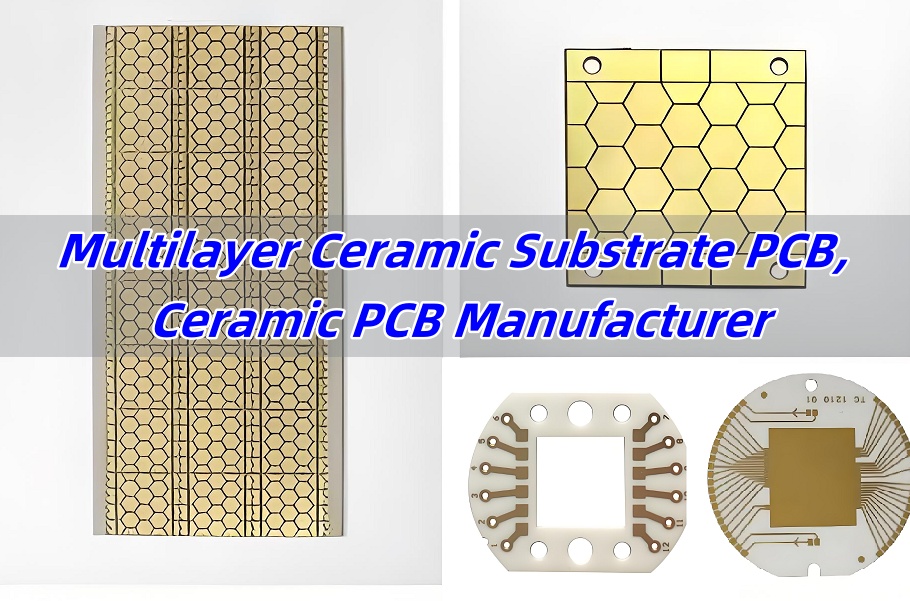
Multilayer Ceramic Substrate PCB, Ceramic PCB Manufacturer
Tuesday, April 15th, 2025

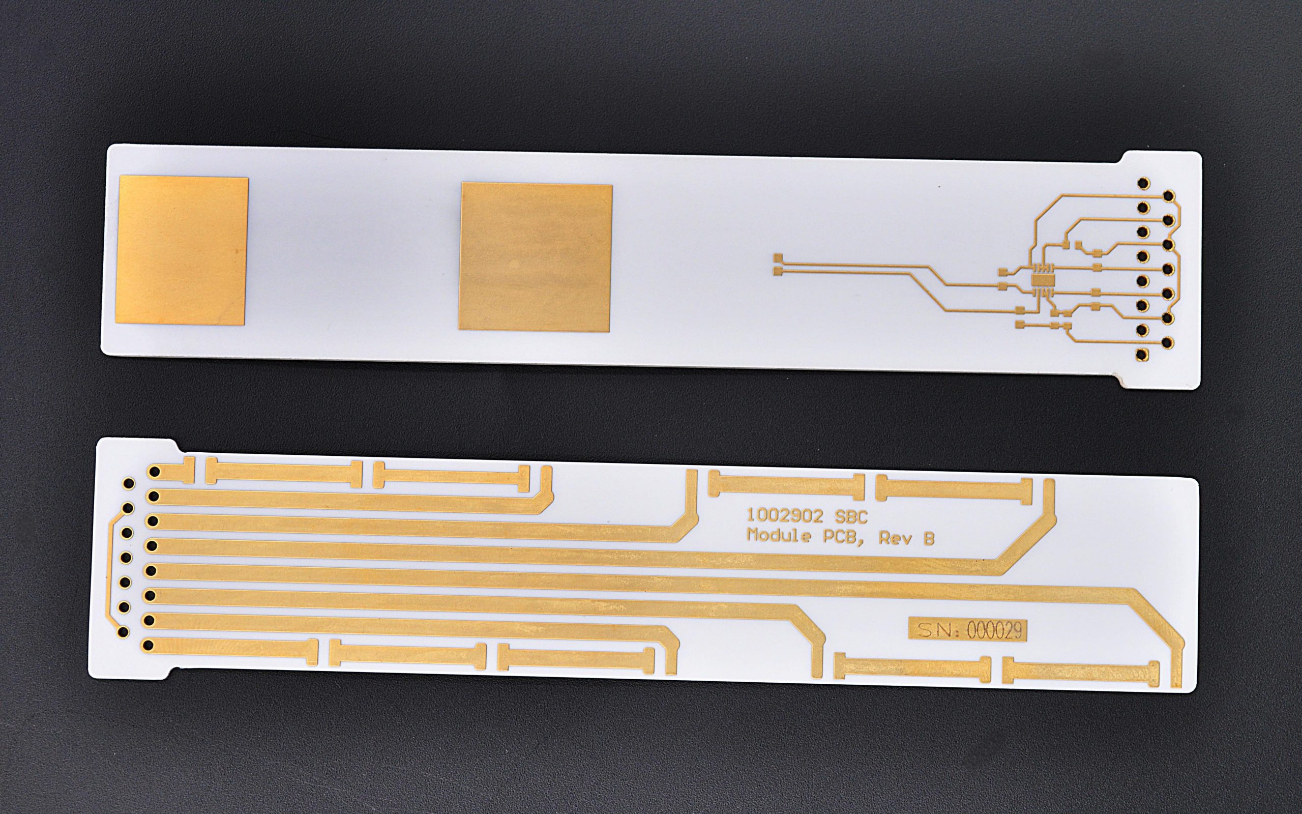
With nearly two decades of experience, EBest Circuit (Best Technology) has become one of the most reliable ceramic PCB manufacturers in Asia. We specialize in high-quality ceramic substrate PCBs for a wide range of industries. From automotive to aerospace, from LED lighting to power electronics—we support innovation with strong technical backing and fast delivery.

We don’t just offer boards; we offer tailored solutions. Our team listens carefully, moves quickly, and delivers results. Whether you need AlN, Al₂O₃, or multilayer ceramic PCB, we’ve got your back.

Multilayer Ceramic Substrate PCB, Ceramic PCB Manufacturer

What Is a Ceramic Substrate PCB?

A ceramic substrate PCB is a circuit board made using ceramic materials as the base instead of traditional resins. Unlike FR-4 or other standard materials, ceramics offer excellent heat resistance, thermal conductivity, and mechanical strength.

They’re not just tough—they’re smart. Ceramics can carry high-frequency signals without distortion. They also handle high power loads with ease, which is why they’re often used in power modules and high-speed communication systems.

Ceramic Substrate PCB Types

Ceramic PCBs vary based on two main categories: materials and production techniques.

1. Divided by Materials

  • Aluminum Nitride (AlN) PCB

Aluminum nitride PCB is favored for its exceptional thermal performance. Its thermal conductivity ranges from 170 to 230 W/m·K, which is much higher than FR4 or even alumina. It’s often used in power devices, RF modules, and LED lighting. This type also provides strong insulation and good mechanical stability.

  • Alumina (Al2O3) PCB

Alumina PCBs are the most common type. They offer a balanced mix of electrical insulation, mechanical strength, and cost-effectiveness. They’re available in 96%, 99%, or 99.6% purity levels. The higher the purity, the better the thermal and electrical properties. These boards are widely used in automotive sensors, LED lighting, and industrial controls.

  • Beryllium Oxide (BeO) PCB

BeO PCBs offer the highest thermal conductivity among ceramic materials—up to 300 W/m·K. However, due to safety concerns during manufacturing, it’s less popular today. Still, for very specific military or aerospace projects, it’s an option. At EBest Circuit (Best Technology), we generally recommend safer materials like AlN or Alumina for most projects.

  • Silicon Nitride (Si₃N₄) PCB

Silicon nitride offers high strength and fracture toughness. It handles heavy vibration and thermal shock better than others. It performs well in both high-temperature and high-load environments.

  • Silicon Carbide (SiC) PCB

SiC gaining attention in high-demand environments like electric vehicles and aerospace systems. It offers thermal conductivity in the range of 80 to 180 W/m·K, along with excellent chemical and radiation resistance.

  • Zirconia (ZrO₂) PCB

Zirconia is known for its toughness and wear resistance. ZrO₂ is used in environments requiring abrasion resistance, such as medical implants, aerospace sealing systems, or sensor housings. It’s not as popular for power electronics but fills special roles where durability matters more than heat dissipation.

2. Divided by Manufacturing Techniques

  • Thick Film Ceramic Substrate PCB

These use screen-printing to apply conductive and dielectric pastes onto the ceramic surface. It’s reliable, cost-effective, and great for low to medium-volume production. The conductor is usually silver or gold. This type works well for sensors and power hybrid circuits. They also support multilayer designs.

  • Thin Film Ceramic PCB

This method uses vacuum deposition and photolithography. It’s precise and supports very fine lines and spaces. Thin-film PCBs are more expensive but deliver unmatched performance in miniaturized devices, such as medical implants or RF modules.

  • DBC Ceramic PCB (Direct Bonded Copper)

DBC PCBs bond copper directly onto a ceramic surface through a high-temperature process. The copper layer is thick and can carry high currents. They are suitable for power semiconductors and automotive applications. They also offer strong adhesion and excellent heat spreading.

  • DPC Ceramic PCB (Direct Plated Copper)

DPC PCBs are made by plating copper directly onto the ceramic using a chemical process. They can achieve finer features than DBC and are suitable for high-frequency or miniaturized devices.

Multilayer Ceramic Substrate PCB, Ceramic PCB Manufacturer
  • HTCC Ceramic PCB (High-Temperature Co-fired Ceramic)

HTCC involves firing a mix of ceramic and metal powders at over 1600°C. It’s durable and works in harsh environments. HTCC PCBs are commonly used in military and aerospace industries due to their stability under extreme conditions.

  • LTCC Ceramic PCB (Low-Temperature Co-fired Ceramic)

LTCC is similar to HTCC but fired at a lower temperature (around 850°C). This process allows for the embedding of passive components, which saves space. It’s perfect for compact, multi-functional devices, especially in telecom and satellite systems. Both HTCC and LTCC ceramic substrate can made into multilayers.

  • AMB Ceramic PCB (Active Metal Brazing)

AMB PCBs use an active brazing technique to bond copper and ceramic. This method provides better bonding strength than DBC and is ideal for high-load applications like electric vehicles.

Technical Specification of Beryllium Oxide (BeO) Ceramic Substrate

Material PropertyUnitValue
ColorWhite
Medium grain sizeum3-5
Surface roughness (Ra)um0.3-0.5
DensityKg/m33010
Rate of water absorption%0
Bending strength4 point method (40x4x3mm3)Mpa400
Dual ring method (0.63mm substrate thickness)Mpa500
Thermal conductivity (20-100℃)W/m-k220-250
Specific heatJ/kg.K800
Coefficient of Linear expansion1*E-6 / K5.1-8.9
Dielectric constant 6-7
Dielectric loss factor (1 MHz)1*E-30.3
Breakdown Voltage2.0mm substrateKV/mm34
1.0mm substrate17
0.635mm substrate11
Volume resistivity20℃Ohm * cm

Technical Specification of Silicon Nitride (Si₃N₄) Ceramic Substrate

Material PropertyUnitValue
ColorGray, White, Off-White
Medium grain sizeum3-5
Surface roughness (Ra)um0.3-0.5
DensityKg/m33120-3220
Rate of water absorption%0
Bending strength4 point method (40x4x3mm3)Mpa147
Dual ring method (0.63mm substrate thickness)Mpa490
Thermal conductivityW/m-k18.42
Specific heatJ/kg.K710
Coefficient of Linear expansion (20-1000℃)10-6/℃2.8-3.2
Dielectric constant 9.4-9.5
Dielectric loss factor (1 MHz)1*E-30.3
Breakdown Voltage2.0mm substrateKV/mm34
1.0mm substrate17
0.635mm substrate11
Volume resistivity20℃Ohm * m1.4*105
500℃Ohm * m4*108

Technical Specification of Silicon Carbide (SiC) Ceramic Substrate

Material PropertyUnitValue
ColorBlack
Medium grain sizeum3-5
Surface roughness (Ra)um0.3-0.5
DensityKg/m33220
Rate of water absorption%0
Bending strength4 point method (40x4x3mm3)Mpa400
Dual ring method (0.63mm substrate thickness)Mpa500
Thermal conductivityW/m-k83.6
Specific heat-106℃J/kg.K399.84
107℃472.27
247℃1266.93
Coefficient of Linear expansion (20-1000℃)10-6/℃6.28-9.63
Dielectric constant 7
Dielectric loss factor (1 MHz)1*E-30.3
Breakdown Voltage2.0mm substrateKV/mm34
1.0mm substrate17
0.635mm substrate11
Volume resistivity20℃M * cm102

Technical Specification of Zirconia (ZrO₂) Ceramic Substrate

Material PropertyUnitValue
ColorWhite
Medium grain sizeum3-5
Surface roughness (Ra)um0.3-0.5
DensityKg/m35850
Rate of water absorption%0
Bending strength4 point method (40x4x3mm3)Mpa380
Dual ring method (0.63mm substrate thickness)Mpa500
Thermal conductivityW/m-k2.09
Specific heatJ/kg.K563.89
Coefficient of Linear expansion (20-1000℃)10-6/℃6.5-11.2
Dielectric constant 27
Dielectric loss factor (1 MHz)1*E-30.3
Breakdown Voltage2.0mm substrateKV/mm34
1.0mm substrate17
0.635mm substrate11
Volume resistivity1000℃Ohm * cm104
1700℃Ohm * cm6-7

For technical specifications of Al2O3 and AlN, please click here to view the details.  

What Is the Difference Between Ceramic Substrate and FR-4?

PropertyCeramic Substrate PCBFR-4 PCB
Material Composition  Inorganic (e.g., Al₂O₃, AlN, Si₃N₄)Organic (Epoxy resin + fiberglass)
Thermal ConductivityHigh (AlN: 170–230 W/m·K, BeO: up to 300 W/m·K)Low (~0.3–0.5 W/m·K)  
Operating TemperatureUp to 800°C or moreLimited to ~130–150°C
Electrical InsulationExcellent and stableModerate
Dielectric ConstantLow and stable (AlN ~8.5, Al₂O₃ ~9.8)Higher and less stable (~4.2–4.8)
Moisture AbsorptionNone (non-porous)Yes (hygroscopic)
Mechanical StrengthHigh (brittle but rigid)Good flexibility and toughness
Thermal Expansion (CTE)Very low (~5–7 ppm/°C)Higher (~14–17 ppm/°C)
RF / Microwave PerformanceExcellent (low loss, stable dielectric)Poor to average (higher signal loss)
PriceHigherLower
ApplicationFocus High-power, high-reliability systems (LEDs, lasers, RF)General-purpose, consumer electronics  
Design FlexibilityLess flexible, requires precise processingVery flexible, supports complex multilayer structures

How Thick Is a Ceramic Substrate?

Ceramic substrate PCBs come in various thicknesses, depending on the material and application. The most commonly used thicknesses range from 0.25 mm to 3.0 mm. However, special requests can push this range even further.

  • For alumina, the standard thicknesses are 0.25 mm, 0.38 mm, 0.5 mm, 0.635 mm, 1.0 mm, and 1.5 mm. These sizes work well for LED packages and power control boards.
  • Aluminum nitride substrates are typically used in 0.38 mm to 1.0 mm thicknesses. The thinner sheets are used in RF circuits, while thicker ones help in thermal management and mechanical support.
  • Silicon nitride and silicon carbide can also be customized in terms of thickness. Some high-strength applications require boards thicker than 2 mm to add mechanical stability.
  • For LTCC and HTCC processes, the thickness can vary as layers are stacked. After sintering, the final board may be thinner than expected due to shrinkage. Designers often specify individual layer thicknesses from 100 µm to 300 µm before lamination.

Factors Affect Ceramic Substrate PCB Price

A ceramic substrate price can be varied depends on the material and process used. Here is a detailed explanation.

1. Material Type

Alumina is the most cost-effective, followed by aluminum nitride. Silicon nitride, silicon carbide, and beryllium oxide are more expensive due to material costs and production challenges.

2. Board Size and Thickness

Larger boards cost more to produce. Thicker substrates also require more raw material and longer sintering times, increasing the cost.

3. Layer Count

Single-layer ceramic PCBs are cheaper. Multilayer designs need more lamination and alignment, raising both time and processing costs.

4. Metallization Method

The choice between thick film, DPC, DBC, or HTCC has a big impact. DPC and DBC processes require specialized equipment, so they are more expensive than thick film types.

5. Tolerances and Precision

If your application requires tight tolerances or fine trace widths, this will increase the cost. More precise laser cutting, printing, or etching takes longer and demands higher quality control.

6. Volume

Like most products, higher quantities reduce the per-unit cost. Low-volume or prototype runs are usually priced higher due to tooling and setup.

7. Surface Finish and Testing

Optional services such as ENIG, silver plating, or 100% electrical testing will raise the overall price.

In summary, the price of a ceramic substrate PCB depends on the complexity, material, and quality requirements. While they cost more than FR-4 boards, their performance and longevity often justify the higher investment.

What Is a Ceramic PCB Used For?

  • High-brightness and long-lifetime lighting
  • Inverters
  • IGBTs
  • Motor drives
  • Imaging systems
  • Implants
  • Diagnostics
  • Telecom
  • Antennas
  • Filters
  • Base stations
  • EV batteries
  • Sensors
  • Control units
  • Aerospace
  • Radar systems
  • Satellite modules

Multilayer Ceramic PCB Manufacturing Process

Multilayer ceramic PCBs are built using different methods than traditional FR-4 boards. The most popular technique is the thick film, HTCC or LTCC process, which allows stacking multiple ceramic layers with embedded circuits. Here’s a step-by-step look at how they’re made:

1. Ceramic Tape Casting

First, thin ceramic tapes (called green sheets) are cast using alumina, aluminum nitride, or other ceramic powders mixed with binders and solvents. These tapes are then dried and punched to create holes for vias.

2. Via Filling and Screen Printing

Vias are filled with conductive pastes such as gold, silver, or tungsten. Then, a conductive pattern is printed on each layer using screen printing or sputtering techniques.

3. Layer Alignment and Lamination

Multiple layers are stacked together carefully, with precise alignment. They are then laminated under pressure and heat, forming a compact structure ready for sintering.

4. Sintering or Firing

In this step, the laminated structure is fired in a high-temperature furnace—up to 1,600°C for HTCC or 850°C for LTCC. This burns off the organic materials and solidifies the ceramic and metal layers.

5. Metallization and Plating

After sintering, the external layers are coated with surface finishes like silver, gold, ENIG, or nickel. These finishes improve solderability and prevent oxidation.

6. Laser Cutting and Drilling

Final shaping is done using CO₂ or UV lasers. This step defines the board outline and makes precise holes for connectors or mounting.

7. Inspection and Testing

Each board undergoes dimensional inspection, electrical testing, and sometimes X-ray analysis to check for internal defects or misalignments.

Why Choose EBest Circuit (Best Technology) as Your Ceramic PCB Manufacturer?

You’re not just buying a board. You’re choosing a partner. At EBest Circuit (Best Technology), we offer:

  • Free ceramic substrate technical consultation
  • In-house production for better lead times
  • 100% electrical testing before shipping
  • Rapid prototyping and mass production
  • Custom designs for all industries
  • Friendly support team that speaks your language
  • Military-grade quality
  • ISO13485, IATF16949, AS9100D certificated
  • No minimum order quantity requirement
  • 5 years quality assurance

Let us help bring your next high-performance product to life. Whether it’s Aluminum Nitride PCB, Alumina, or multilayer ceramic PCB, we’re ready to deliver results you can count on.

You may also like

Al2O3 Ceramic PCB Fabrication & Ceramic PCB Manufacturer
Tuesday, March 4th, 2025

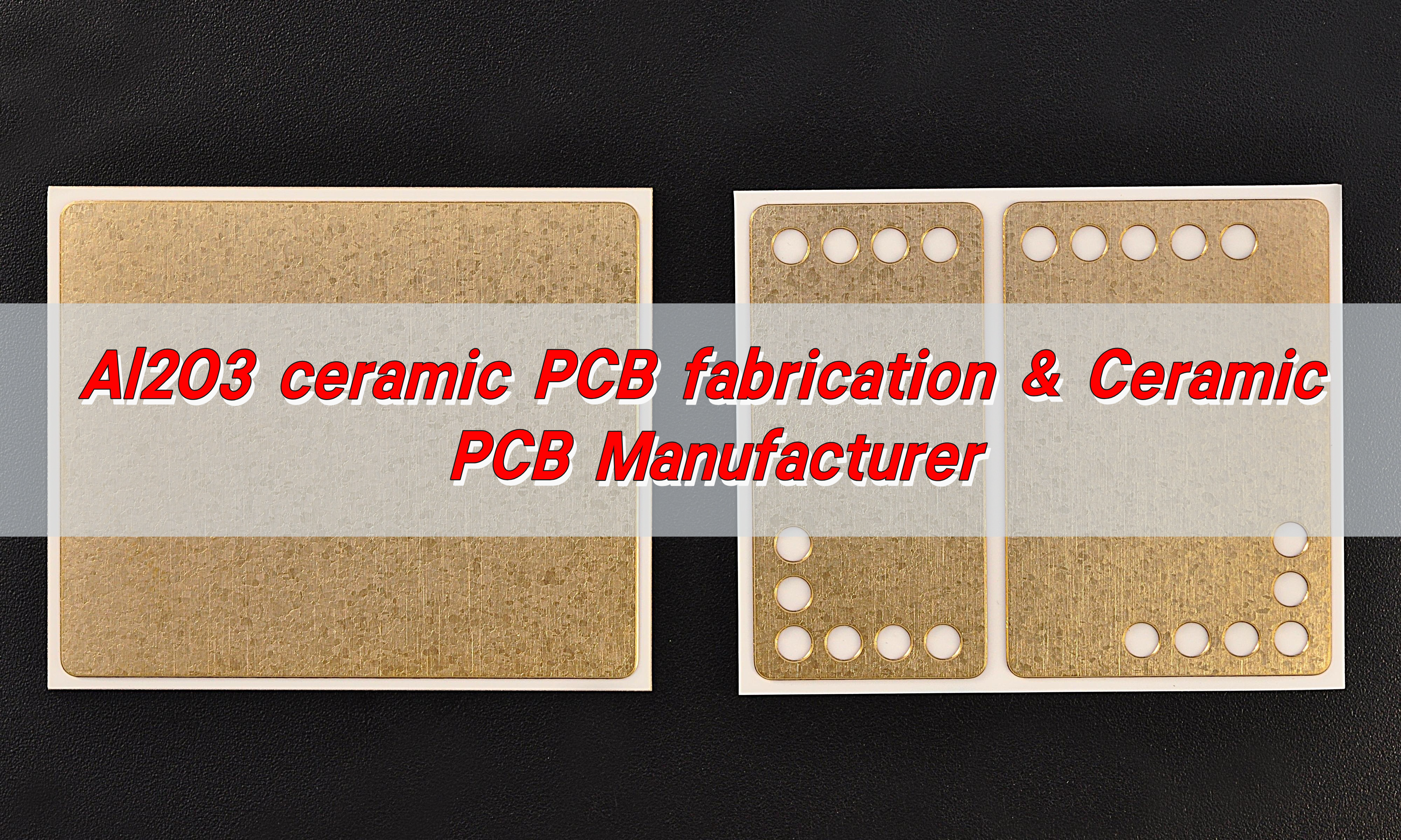
Al2O3 ceramic PCB fabrication is the process of producing printed circuit boards using alumina (Al2O3) ceramic substrates. Alumina ceramics have high mechanical strength, hardness, heat resistance, electrical insulation and corrosion resistance, and are one of the most cost-effective materials in the electronic packaging industry.

Al2O3 Ceramic PCB Fabrication & Ceramic PCB Manufacturer

Unlike ordinary PCBs, ceramic PCBs are made by directly bonding copper foil and ceramic substrates under high temperature environments. They have strong bonding strength, the copper foil will not fall off, and have high reliability and performance stability under high temperature and high humidity environments.

As a ceramic PCB manufacturer with 18 years of manufacturing experience, BEST Technology has accumulated rich professional strength in the manufacturing of alumina ceramic PCBs. In terms of manufacturing technology, it adopts advanced manufacturing processes to ensure that each alumina ceramic PCB meets high quality standards.

What is Alumina Ceramic PCB?

Alumina ceramic PCBs are circuit boards made using aluminum oxide (Al₂O₃) as the substrate material. This type of PCB is known for its excellent thermal management, high insulation resistance, and mechanical strength.

Compared to conventional FR-4 boards, alumina ceramic PCBs offer better heat dissipation, making them ideal for high-power applications like LED lighting, automotive electronics, and aerospace systems.

Unlike standard PCB materials, alumina ceramic is highly resistant to chemical corrosion and environmental stress. It can endure extreme temperatures without degrading, ensuring long-term reliability in demanding conditions.

How Do You Make Al₂O₃ Ceramic PCB?

Fabricating an alumina ceramic PCB requires a specialized manufacturing process. Unlike FR-4 boards, which are processed using laminates, ceramic PCBs are created through advanced sintering techniques.

The process typically involves:

  • Material Preparation – High-purity alumina ceramic is selected based on thermal and electrical requirements.
Al2O3 Ceramic PCB Fabrication & Ceramic PCB Manufacturer
  • Substrate Formation – The ceramic is shaped and sintered at high temperatures to achieve a dense, strong structure.
  • Metallization – Copper, silver, or gold is deposited onto the ceramic surface using thick-film or thin-film technology.
  • Circuit Patterning – The conductive layer is etched or laser-processed to define the circuit layout.
  • Component Assembly – SMD or through-hole components are mounted using high-temperature soldering or wire bonding.
  • Final Testing – The finished PCB undergoes electrical and thermal testing to ensure optimal performance.

This fabrication method results in a robust, high-performance PCB with excellent electrical insulation and thermal efficiency.

What Are the Advantages of Alumina Ceramic PCB?

Al₂O₃ ceramic PCBs come with a range of benefits that make them superior to traditional materials.

  • Exceptional Heat Dissipation – The ceramic substrate effectively transfers heat away from components, preventing overheating.
  • High Mechanical Strength – Alumina ceramic is incredibly strong, resisting mechanical stress and impact.
  • Superior Electrical Insulation – This material prevents electrical leakage, ensuring stable circuit performance.
  • Corrosion Resistance – Unlike metal-based PCBs, alumina ceramic does not rust or degrade over time.
  • Dimensional Stability – It maintains its structure under extreme conditions, including high temperatures and humidity.

These advantages make alumina ceramic PCBs a top choice for advanced electronic applications requiring reliability and efficiency.

What Are the Materials Used in Ceramic Substrate?

Ceramic PCBs can be made using different types of ceramics, each offering unique properties:

  • Alumina (Al₂O₃) – The most widely used ceramic material, known for its affordability and strong thermal performance.
Al2O3 Ceramic PCB Fabrication & Ceramic PCB Manufacturer
  • Aluminum Nitride (AlN) – Offers higher thermal conductivity than alumina but comes at a higher cost.
  • Beryllium Oxide (BeO) – Provides outstanding thermal properties but has limited use due to toxicity concerns.
  • Silicon Carbide (SiC) – Used in specialized high-temperature applications.

Each material is selected based on specific electrical, thermal, and mechanical requirements.

Is Alumina Ceramic Better Than Zirconia Ceramic?

Alumina and zirconia ceramics are both high-performance materials, but they serve different purposes.

  • Alumina Ceramic (Al₂O₃) – Offers better thermal conductivity, making it ideal for PCBs that require efficient heat dissipation.
  • Zirconia Ceramic (ZrO₂) – Has superior mechanical toughness and is often used in wear-resistant applications.

For electronic circuit boards, alumina is the preferred choice due to its balance of strength, electrical insulation, and heat management.

How Thick is Alumina Ceramic PCB?

The thickness of an alumina ceramic PCB varies based on application needs. Typically, the substrate thickness ranges from 0.25mm to 5mm, depending on thermal and mechanical requirements.

Thinner PCBs are used in compact electronics, while thicker substrates are chosen for heavy-duty applications requiring robust performance.

What is the Difference Between Al₂O₃ Ceramic PCB and FR-4?

FR-4 and alumina ceramic PCBs are widely used, but they differ in key ways:

  • Material CompositionFR-4 is a fiberglass-reinforced epoxy, while alumina ceramic is a solid ceramic substrate.
Al2O3 Ceramic PCB Fabrication & Ceramic PCB Manufacturer
  • Thermal Conductivity – Alumina ceramic dissipates heat much more efficiently than FR-4.
  • Durability – Ceramic PCBs can withstand harsh environments, whereas FR-4 boards are more prone to degradation.
  • Electrical Performance – Alumina has superior insulation and minimal signal loss, making it ideal for high-frequency circuits.

For applications where heat management and longevity are critical, alumina ceramic PCBs offer a clear advantage.

What Are the Applications of Alumina Ceramic PCB?

Due to their exceptional properties, alumina ceramic PCBs are used in various industries:

  • LED Lighting – Ensures efficient heat dissipation for high-brightness LEDs.
  • Power Electronics – Used in high-voltage circuits requiring stability and durability.
  • Automotive Electronics – Found in electric vehicles, sensors, and power management systems.
  • Aerospace & Defense – Used in radar, communication, and avionics due to reliability under extreme conditions.
  • Medical Devices – Integrated into imaging systems and surgical instruments for their biocompatibility and precision.

As electronic devices continue to demand higher efficiency and performance, alumina ceramic PCBs are becoming an essential part of modern technology.

Conclusion:

Al₂O₃ ceramic PCBs provide a superior solution for applications requiring durability, thermal efficiency, and electrical reliability. Compared to traditional FR-4 boards, they offer better heat dissipation, mechanical strength, and longevity.

For high-quality alumina ceramic PCB fabrication, choosing the right manufacturer is crucial. At EBest Circuit (Best Technology), we specialize in custom ceramic PCBs designed to meet the most demanding requirements. Contact us at sales@bestpcbs.com to discuss your project needs!

You may also like

Aluminum Nitride PCB | Aluminum Nitride Ceramic PCB Design
Thursday, October 10th, 2024

What is Aluminum Nitride PCB?

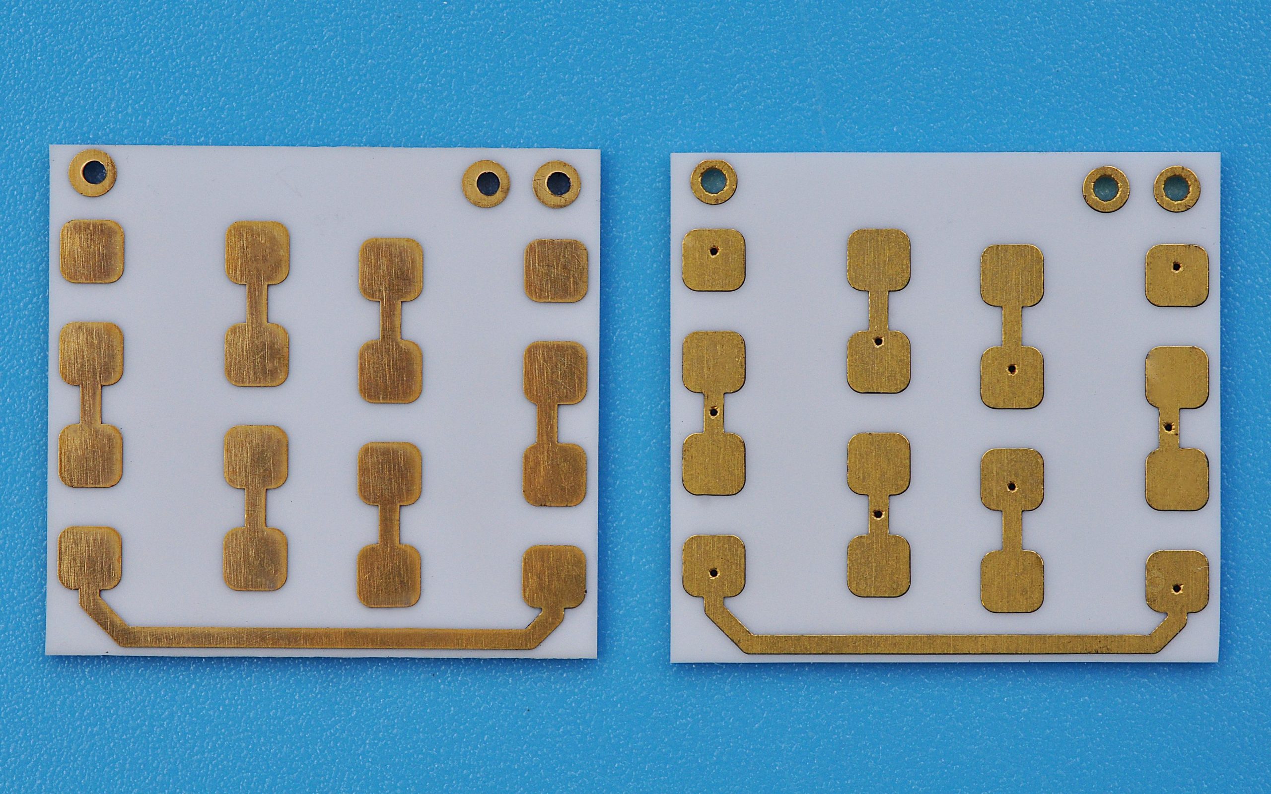
Aluminum nitride PCB also known as Aluminum nitride ceramic PCB or short for AlN PCB. It is a high-performance circuit board made from aluminum nitride ceramic, a material known for its exceptional thermal conductivity and electrical insulation properties. These boards are commonly used in industries where efficient heat dissipation is crucial, such as in power electronics, LED applications, and high-frequency devices. AlN PCBs are gaining popularity due to their ability to withstand extreme temperatures.

Aluminum Nitride PCB | Aluminum Nitride Ceramic PCB

Benefits of AlN PCBs

One of the key advantages of AlN PCBs is their excellent thermal conductivity, which helps prevent overheating in electronic components. With exceptional thermal conductivity of 170 W/mK, strong dielectric strength, and a low thermal expansion coefficient (CTE <4 ppm/°C), AlN is widely used in applications like high-power LEDs, lasers, high-current switches, and even ultra-low temperature vacuum electronics such as those in quantum computing. In addition to these features, AlN offers the same benefits as other ceramic materials, including rigidity, environmental and chemical resistance, and 0% water absorption.

Key reasons for choosing Aluminum Nitride over other PCB materials include:

  • Outstanding thermal conductivity of 170 W/mK
  • Excellent dielectric properties
  • High operating temperatures exceeding 350°C
  • Low thermal expansion coefficient (<4 ppm/°C)
  • Compact designs due to better integration
  • Hermetically sealed packages with 0% water absorption
  • Minimal to no outgassing

What is the Thermal Conductivity of Aluminum Nitride PCB?

‌The thermal conductivity of aluminum nitride PCB ranges from 170-230W/(m·K).

The high thermal conductivity of aluminum nitride PCB is due to its unique structure and chemical composition. The thermal conductivity of aluminum nitride ceramic substrate is 2-3 times higher than that of traditional alumina ceramics and silicon-based ceramics, and 10-20 times higher than that of titanium substrate. This high thermal conductivity allows them to effectively dissipate heat from high-power electronic components, preventing overheating and ensuring stable performance. The ability to manage heat efficiently makes AlN PCBs an ideal choice for applications that generate a significant amount of heat, such as power modules, LEDs, and RF components. In comparison to other materials like aluminum oxide, which has lower thermal conductivity (around 20-30 W/mK), aluminum nitride stands out as a top choice for heat-sensitive applications.

Factors affect thermal conductivity of AlN PCB

Although the theoretical thermal conductivity of AlN is extremely high, its performance in practical applications is limited by a number of factors, mainly including:

  • Microstructure

Phonon scattering is a key mechanism for heat conduction. Grain boundaries, interfaces, second phases, and defects can all affect the mean free path of phonons, thereby influencing thermal conductivity. High-purity, low-defect single-crystal AlN has a longer phonon mean free path and higher thermal conductivity.

  • Oxygen Impurity Content

AlN’s strong affinity with oxygen leads to the easy introduction of oxygen impurities, which form alumina films and lattice defects, such as aluminum vacancies. These significantly reduce the phonon mean free path, lowering thermal conductivity. When the oxygen concentration is below 0.75%, oxygen atoms primarily replace nitrogen atoms in the lattice; however, exceeding this concentration causes aluminum vacancies to disappear and results in the formation of extended defects, further affecting thermal conductivity.

  • Sintering Process and Additives

By selecting appropriate sintering additives (such as Y₂O₃-Li₂O, Y₂O₃-CaC₂ composite systems), densification can be achieved at lower temperatures, while reducing the formation of oxygen impurities and second phases, effectively improving the thermal conductivity of AlN ceramics. These additives help purify grain boundaries and optimize the microstructure, facilitating more efficient phonon transmission.

What is Aluminum Nitride PCB Used For?

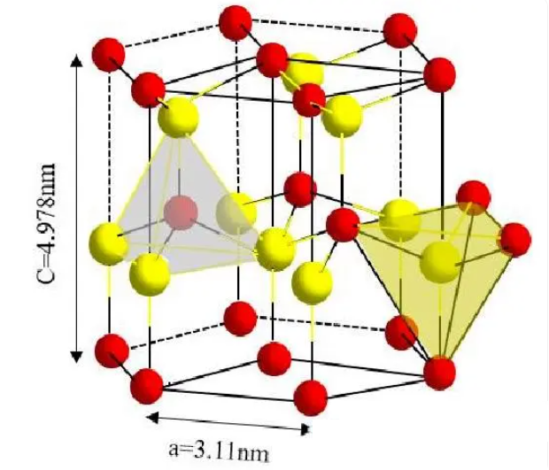
Aluminum nitride as a stable hexagonal wurtzite covalent bond compound, has shown extensive application potential in the field of electronics and optoelectronics due to its unique physical and chemical properties. Its crystal structure takes AlN4 tetrahedron as the basic unit, space group P63mc, belongs to the hexagonal crystal system, which gives AlN a series of excellent properties and use in advanced applications.

Aluminum Nitride PCB | Aluminum Nitride Ceramic PCB

Some common applications include:

  • Optical Communication
  • Integrated Circuits and High-Power Electronic Devices
  • Power Electronics
  • Wafer chips
  • Epoxy Resin Packaging
  • Optical Devices and Piezoelectric Devices
  • Industrial Materials
  • Acoustic Devices
  • Aerospace
  • Military

Why is Aluminum Nitride Expensive?

The high cost of aluminum nitride PCBs stems from several factors.

First of all, the raw material cost of aluminum nitride PCB is higher. The preparation of aluminum nitride powder requires high purity raw materials, synthesis methods include direct nitriding method, carbothermal reduction method, self-propagating high temperature synthesis and chemical vapor deposition method, etc. These methods have high requirements on equipment and technology, resulting in higher costs.

Secondly, the production process is complicated. The preparation process of aluminum nitride PCB is complex, including multiple steps such as molding and sintering, which has high requirements for equipment and technology and a high production threshold.

Finally, the market demand is large. Aluminum nitride PCB in power electronics, communication equipment, automotive electronics and other fields have a wide range of applications, especially in high power, high frequency and other occasions, its excellent heat dissipation and insulation performance can not be replaced, resulting in short supply in the market, the price of natural rising.

Aluminum Nitride PCB vs. Alumina Oxide PCB

Both aluminum nitride (AlN) and alumina oxide (Al2O3) are ceramic materials used in PCB manufacturing, but they differ significantly in terms of performance. AlN offers superior thermal conductivity, typically 170-230 W/mK, compared to aluminum oxide’s lower range of 20-30 W/mK. This makes AlN the better option for applications requiring efficient heat dissipation, such as high-power electronics and LED lighting.

However, aluminum oxide is more cost-effective and is often used in applications where high thermal conductivity is not as crucial. While Al2O3 provides good electrical insulation and is easier to produce, it may not perform as well in heat-sensitive environments as AlN. Therefore, the choice between AlN and Al2O3 depends on the specific thermal and budgetary requirements of the application. Here are the parameters of AlN and Al2O3 materials:

ParameterAluminum Nitride (AlN)Alumina Oxide (Al2O3)
Thermal conductivity170-230 W/m.k24-30 W/m.k
Dielectric constant8.89.2-10
Dielectric strength15-25kV/mm10-15kV/mm
Temperature resistance1000-1500C1000-1200C
CTE4.0 ppm/K6.5-7 ppm/K
Flexural strength450MPa320MPa
Dielectric breakdown voltage14 V/m10 V/m

AlN Ceramic PCB Design Considerations

When designing an aluminum nitride PCB, several factors need to be considered to optimize performance:

1. Trace Width

The trace width on AlN PCBs should be a minimum of 10 mils. This ensures that the conductor cross-section is sufficient to handle the current and heat dissipation needs. Given the thermal advantages of AlN, wider traces help in spreading heat more efficiently, minimizing the risk of overheating in power-dense applications.

2. Trace Clearance

Clearances between adjacent traces should be at least 8 to 10 mils. AlN PCBs often work with higher voltage levels, making spacing critical to prevent arcing or dielectric breakdown. In high-power designs, careful spacing between traces reduces the likelihood of signal interference and maintains the board’s insulation integrity.

3. Via Pads

For via pads, a minimum diameter of 16 mils is recommended. This provides sufficient area for stable soldering and ensures proper electrical connection through the via. Depending on the board’s application, larger via pads may be necessary to accommodate higher currents or thermal dissipation needs. Via sizing should also account for assembly techniques, such as reflow soldering or thermal management features, like thermal vias, which enhance heat transfer away from components.

4. Pad Geometry Adjustments

Unlike FR-4 designs, AlN PCBs often require specific adjustments in pad geometries. The mechanical and thermal properties of AlN are quite different from those of traditional PCBs. The expansion rate, hardness, and substrate fragility mean that pad designs should allow for thermal expansion and contraction without causing stress fractures. Proper pad design also ensures better solder joint reliability, particularly for components exposed to continuous thermal cycling.

5. Gold Plating for Wire Bonding Pads

In high-performance applications, wire bonding is often used, and gold plating is a preferred surface finish for wire bonding pads. The use of gold provides a stable, corrosion-resistant surface that improves bond integrity and longevity. Wire bonding is especially critical in high-frequency, high-reliability devices, where the connections must maintain integrity under thermal stress or in harsh environments.

Aluminum Nitride PCB | Aluminum Nitride Ceramic PCB

6. Component and Solder Matching

All components and solder materials must match the electrical and mechanical properties of the AlN substrate. Mismatches in thermal expansion between the PCB material and components can lead to stress, causing cracking or delamination. It’s important to select components and solder that can withstand high temperatures and thermal cycles while maintaining compatibility with AlN’s characteristics, especially in applications like power electronics and RF circuits.

7. Hermetic Sealing and Height Restrictions

For applications requiring hermetic sealing, such as aerospace or medical devices, height restrictions may apply to the components on the PCB. Hermetic seals protect against moisture and environmental contaminants, ensuring long-term reliability in sensitive applications. The overall component height should be kept in line with the sealing requirements, and compact designs are often necessary to meet stringent packaging constraints.

8. Thermal Expansion Management

When attaching large dies or high-power devices, it’s crucial to model and account for thermal expansion. Even though AlN has a low thermal expansion coefficient (<4 ppm/°C), the difference in expansion rates between components and the substrate can create mechanical stress, especially during thermal cycling. Careful design, including flexible connections or underfill materials, can help mitigate these effects.

9. Thermal Vias

Thermal vias are essential for managing heat in high-power applications. By placing thermal vias directly underneath hot components, heat can be efficiently transferred away from sensitive areas, extending the lifespan of both the components and the PCB itself. In many designs, a network of thermal vias is integrated with heat sinks or spreaders to further improve heat dissipation.

10. Surface Finishes and Coatings

Aluminum nitride PCBs can benefit from surface finishes such as electroless nickel immersion gold (ENIG) or immersion silver, which protect the copper traces from oxidation and provide excellent solderability. The choice of surface finish may also depend on the specific application environment and the reliability requirements, especially in high-power or high-frequency circuits.

FAQs About AlN PCBs

1. How durable are aluminum nitride PCBs?

    AlN PCBs are highly durable and can withstand extreme temperatures and harsh environments.

    2. Can AlN PCBs be used in high-frequency applications?

    Yes, aluminum nitride PCBs are well-suited for high-frequency and high-speed applications due to their excellent electrical insulation and low signal loss.

    3. Are aluminum nitride PCBs environmentally friendly?

    While the production process can be resource-intensive, AlN PCBs offer longer lifespans and higher efficiency, which can reduce the environmental impact over time.

    4. How do AlN PCBs compare with metal-core PCBs?

    Metal-core PCBs, such as those with an aluminum core, provide good thermal management but lack the superior electrical insulation of AlN PCBs. AlN PCBs are preferred for applications requiring both high thermal conductivity and insulation.

    5. What industries typically use aluminum nitride PCBs?

    Industries like power electronics, aerospace, automotive, and telecommunications commonly use AlN PCBs for their high-performance needs.

    You may also like