PCB manufacturing PCB manufacturing
Home > Blog

RF PCB Manufacturing

5-in-1 Antenna PCB Layout, Fabrication, and PCBA Assembly
Wednesday, May 27th, 2026

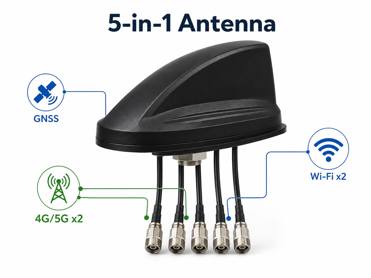
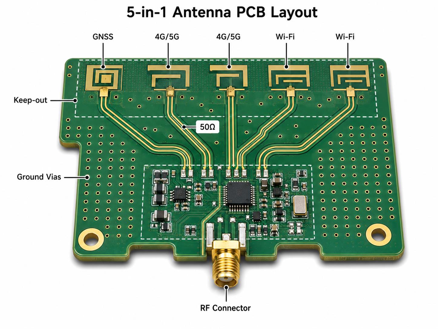
A 5-in-1 antenna usually combines GNSS, 4G/5G cellular, and Wi-Fi signal paths in one antenna unit. It is common in IoT gateways, vehicle trackers, industrial routers, smart transportation devices, and outdoor wireless terminals.

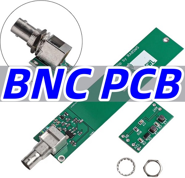
This guide focuses on the checks a PCB/PCBA manufacturer can realistically support before fabrication, assembly, and shipment. In many 5-in-1 antenna PCB and PCBA projects, the antenna is connected through RF interfaces such as SMA connector PCB, SMB PCB, UFL Connector PCB, BNC PCB, or MMCX PCB. If your wireless device requires RF connector assembly, controlled impedance PCB fabrication, or PCBA production review, you can send your Gerber files, BOM, and assembly requirements to sales@bestpcbs.com.

5-in-1 Antenna

What Is a 5-in-1 Antenna?

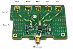
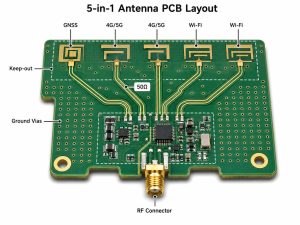
A 5-in-1 antenna is an integrated antenna solution with five wireless signal paths. A common structure includes:

  • 1x GNSS antenna
  • 2x 4G/5G cellular MIMO antennas
  • 2x Wi-Fi MIMO antennas

In a real device, the antenna connects to the PCB assembly through RF connectors, coaxial cables, wireless modules, matching circuits, ESD protection parts, and controlled impedance traces.

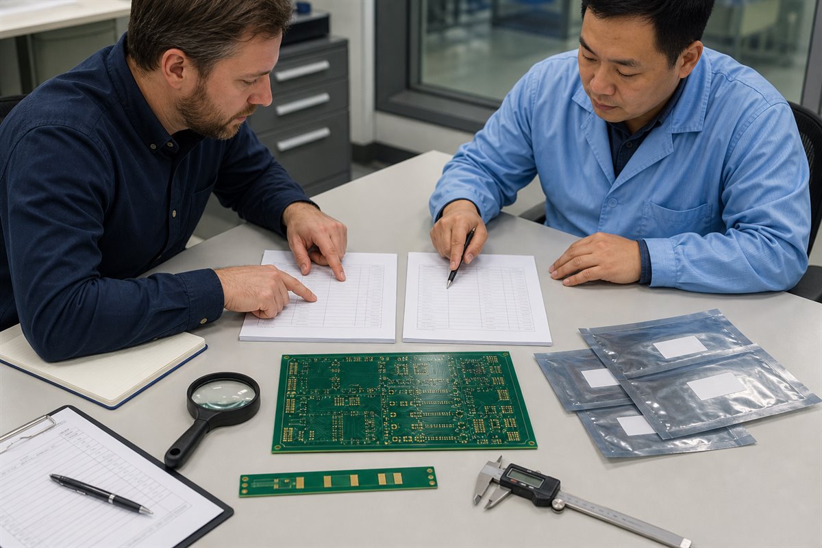
A PCB/PCBA manufacturer does not replace the antenna engineer. Its value is to check whether the PCB files, stackup, impedance notes, RF connector footprint, BOM, assembly drawing, and test requirements are ready for production.

5-in-1 Antenna

Common PCB and PCBA Risks in 5-in-1 Antenna Projects

Problem Found LaterCommon Manufacturing CauseWhat Should Be Checked Early
Weak GNSS receptionPoor RF path control or unclear layout notesGNSS path, impedance note, connector area, module guide
Unstable 4G/5G connectionImpedance mismatch or connector issue50Ω trace, stackup, RF connector footprint
Poor Wi-Fi performanceTrace discontinuity or cable assembly issueWi-Fi RF path, connector placement, coaxial cable route
Prototype works, batch variesStackup changed or impedance not controlledStackup drawing, impedance coupon, fabrication tolerance
RF connector becomes looseWrong footprint or weak pad designConnector datasheet, pad size, solder mask opening
RF matching issueWrong value or misplaced small componentsBOM, placement file, first article inspection
Shielding issuePoor soldering or incomplete groundingShielding can footprint, solderability, ground pads

These problems are expensive because they often appear after SMT assembly or final testing. Early manufacturing review is much cheaper than redesign, rework, or repeated debugging.

What Should Be Checked Before PCB Fabrication?

Before PCB fabrication, the main task is to confirm whether the board data can support stable RF-related production.

1. Stackup

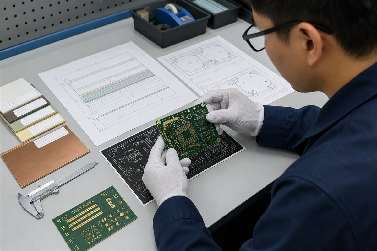
Stackup affects impedance, trace width, return path, and signal loss. For antenna-related products, stackup should be confirmed before production.

Check:

  • Layer count
  • Dielectric thickness
  • Copper thickness
  • RF reference layer
  • Solder mask condition
  • Material availability
  • Impedance tolerance

2. 50Ω RF Trace Requirement

Most GNSS, cellular, and Wi-Fi feed lines use 50Ω controlled impedance. This requirement should be clearly marked in the fabrication notes.

Customers should provide:

  • Target impedance
  • Controlled impedance layer
  • Trace width and spacing
  • Stackup drawing
  • Impedance tolerance
  • Test coupon requirement

Without clear impedance notes, the board may be treated as a normal PCB instead of an RF-controlled board.

3. RF Connector Footprint

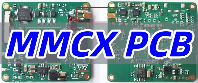
RF connector problems are common in antenna-related PCBA projects. SMA, U.FL, IPEX, MMCX, and board-to-board RF connectors all have specific footprint requirements.

Check:

  • Pad size
  • Ground pad connection
  • Solder mask opening
  • Connector orientation
  • Edge clearance
  • Cable direction
  • Rework space

A small footprint error can cause soldering defects, weak contact, or unstable field performance.

RF Connector Area and Assembly Clearance

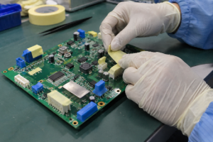
The RF connector area should be reviewed before PCB fabrication and PCBA assembly. For a 5-in-1 antenna product, connector placement and nearby PCB details can affect soldering quality, cable installation, inspection, rework access, and production consistency.

A PCB/PCBA manufacturer can help check whether the connector footprint, solder mask opening, ground pads, board edge clearance, and cable direction match the assembly requirement. If the customer provides a wireless module layout guide or antenna reference design, the manufacturer can also review whether the board files follow the key manufacturing notes.

Check before production:

  • RF connector footprint against the datasheet
  • Pad size and solder mask opening
  • Ground pad connection around the connector
  • Board edge clearance
  • Cable plugging direction
  • Space for manual inspection and rework
  • Coaxial cable bend radius
  • Shielding can footprint and solderability, if used
  • Keep-out notes provided by the module or antenna supplier

This review does not replace antenna tuning, OTA testing, or RF chamber testing. Its purpose is to reduce assembly risk, connector failure, soldering defects, and avoidable layout-to-production problems.

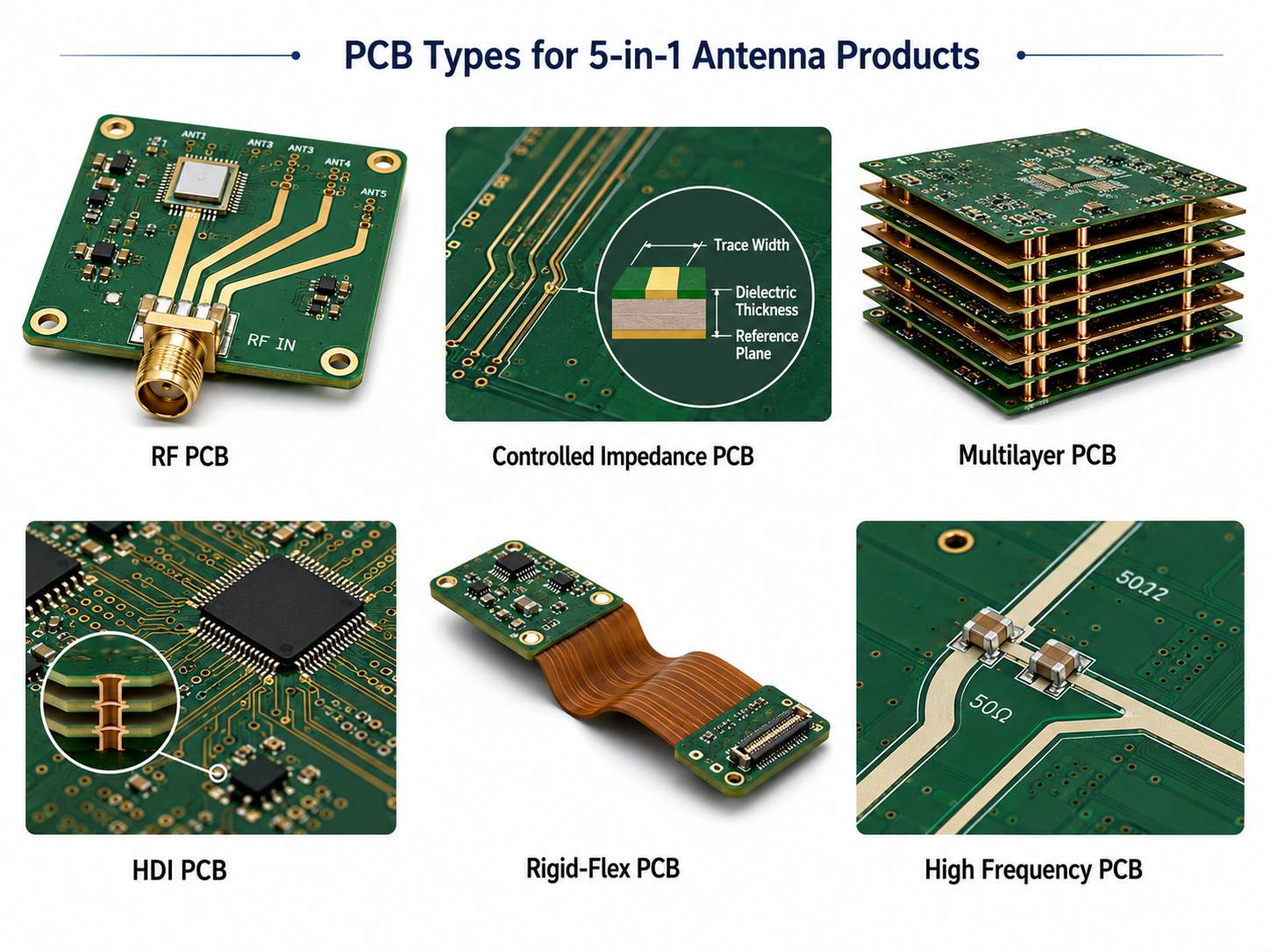
What Types of PCBs Are Used in 5-in-1 Antenna Products?

Different products need different PCB structures. The PCB type should match the RF requirement, space limit, assembly method, and working environment.

PCB TypeTypical UseManufacturing Value
RF PCBAntenna feed lines, wireless modulesBetter RF trace and impedance control
High Frequency PCBHigher-frequency or lower-loss RF pathsMore stable signal transmission
Controlled Impedance PCBGNSS, cellular, Wi-Fi RF tracesKeeps 50Ω signal paths consistent
Multilayer PCBGateways, routers, tracking devicesBetter grounding, routing, and power distribution
HDI PCBCompact wireless devicesSupports fine-pitch modules and dense routing
Rigid PCBIndustrial and outdoor devicesStable structure for connectors and modules
Flexible PCBSpace-limited internal connectionsFits compact mechanical structures
Rigid-Flex PCBMulti-section compact devicesReduces connectors and improves reliability
High-TG PCBAutomotive, outdoor, industrial productsBetter thermal stability
Ceramic PCBSpecial RF or thermal-sensitive modulesGood for high-reliability applications
Metal Core PCBSmart LED or power products with wireless functionHelps thermal management

For many projects, the practical choice is a multilayer controlled impedance PCB. Compact products may use HDI PCB or rigid-flex PCB. Higher-frequency paths may require RF PCB or high frequency PCB.

5-in-1 Antenna

What Should Be Checked During PCBA Assembly?

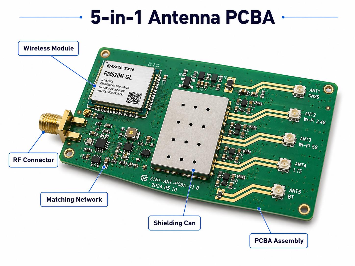
5-in-1 antenna PCBA assembly usually includes RF connectors, wireless modules, small matching components, shielding parts, and coaxial cables. These areas need tighter process control.

RF Connectors

  • Check connector position, solder quality, grounding, mechanical strength, and cable plugging direction. U.FL and IPEX connectors are small and can be damaged by poor soldering or repeated rework.

Wireless Modules

  • Check solder paste volume, stencil opening, reflow profile, placement accuracy, and inspection method. LGA, BGA, castellated, and fine-pitch wireless modules need stable SMT control.

Matching Network Components

  • Small capacitors and inductors near RF paths must match the BOM and placement file. Wrong values or wrong positions can change RF behavior.

Shielding Cans

  • Shielding only works well when grounding and soldering are reliable. Shielding can footprints, solder paste openings, and inspection standards should be confirmed before assembly.

Coaxial Cables and Wire Harnesses

  • Cable direction, bend radius, connector locking, strain relief, and final assembly sequence should be checked before batch production.

First Article Inspection

  • For the first build, inspect connector placement, module alignment, component value, polarity, solder joints, shielding position, and test results before moving to larger quantities.
5-in-1 Antenna

What Testing Should Be Planned Before Shipment?

Testing should be defined before assembly, not after production is finished.

TestPurpose
Bare PCB electrical testCheck opens and shorts
Impedance testConfirm RF trace impedance on test coupon
AOICheck solder joints, polarity, missing parts
X-rayInspect BGA/LGA or hidden solder joints
Functional testConfirm power, module boot, interface communication
RF path continuity checkFind connector or soldering issues
GNSS/Wi-Fi/cellular function checkVerify product-level wireless function
Final assembly inspectionCheck cable, connector, enclosure, label, and package

A PCB/PCBA factory can support production-level tests such as electrical test, impedance test, AOI, X-ray, visual inspection, and functional testing based on customer procedures.

Advanced antenna tests such as OTA, radiation pattern, antenna efficiency, and certification-level RF performance usually require customer fixtures, RF chambers, or third-party labs.

What Files Are Needed for a Faster Quote?

Complete files help the manufacturer review the project faster and quote more accurately.

Send:

  • Gerber or ODB++ files
  • Drill files
  • PCB stackup
  • Controlled impedance requirement
  • BOM with manufacturer part numbers
  • Pick-and-place file
  • Assembly drawing
  • RF connector datasheets
  • Wireless module datasheets
  • Antenna specification
  • Testing requirements
  • Cable or wire harness requirements
  • Order quantity
  • Target delivery schedule

For PCBA projects, BOM quality matters. RF connectors, wireless modules, EOL parts, and alternative components should be checked before batch production.

FAQs About 5-in-1 Antenna PCB and PCBA Manufacturing

Q1: Can a PCB/PCBA manufacturer design the 5-in-1 antenna?
Usually no. A PCB/PCBA manufacturer supports layout review, DFM, impedance control, fabrication, assembly, and testing. Full antenna electromagnetic design should be handled by RF antenna specialists.

Q2: Does a 5-in-1 antenna PCB need controlled impedance?
In most cases, yes. GNSS, cellular, and Wi-Fi RF feed lines commonly require 50Ω controlled impedance.

Q3: Can FR4 be used for 5-in-1 antenna products?
Yes, FR4 can be used when the frequency, loss requirement, and layout structure are suitable. For higher-frequency or lower-loss paths, high frequency PCB materials may be needed.

Q4: What is the most common manufacturing issue?
Common issues include unclear impedance notes, incorrect RF connector footprints, poor grounding, missing assembly clearance, wrong matching components, and poor cable routing.

Q5: What PCB type is commonly used?
Many projects use multilayer controlled impedance PCB. Compact wireless products may use HDI PCB or rigid-flex PCB.

Q6: Can the factory test RF performance?
The factory can support production-level tests. Advanced RF performance testing may require customer fixtures, RF chambers, or third-party RF labs.

In summary, a 5-in-1 antenna product is not difficult only because it uses several wireless functions. The real production challenge is making the PCB and PCBA stable, repeatable, and testable.

Before production, customers should confirm RF trace impedance, stackup, connector footprint, assembly clearance, shielding parts, cable routing, BOM accuracy, and test method. These checks help reduce rework, shorten debugging time, and improve batch consistency.

Best Technology supports RF PCB, high frequency PCB, controlled impedance PCB, multilayer PCB, HDI PCB, rigid-flex PCB, ceramic PCB, metal core PCB, PCB fabrication, PCBA assembly, SMT stencil, wire harness, component sourcing, DFM review, and production testing.

Send your Gerber files, BOM, antenna specification, and project requirements to sales@bestpcbs.com. Our engineering team can review your 5-in-1 antenna PCB and PCBA project before production and help you move from prototype to a more stable manufacturing build.

You may also like

PTFE PCB Manufacturer for High-Frequency Boards
Tuesday, May 19th, 2026

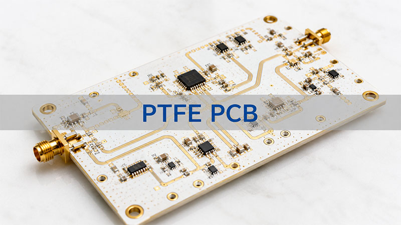
PTFE PCB projects usually come with clear business goals: stable RF performance, reliable fabrication, smooth assembly, and fewer delays before production. For buyers, the key question is not only “What is PTFE?” It is also “Can this manufacturer support my material, stack-up, impedance, RF connector assembly, and delivery needs?”

This guide helps you compare PTFE PCB materials, manufacturing capabilities, application fit, DFM support, and supplier selection factors.

ptfe pcb

What Is a PTFE PCB and Is It Right for Your Project?

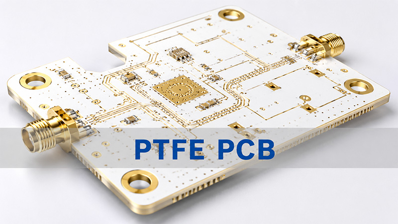
A PTFE PCB is a printed circuit board made with PTFE-based dielectric material. Engineers often choose it for RF, microwave, antenna, radar, and high-frequency communication products.

ItemWhat It Means for Your Project
Material TypePTFE-based high-frequency laminate
Main PurposeLower signal loss and stable RF behavior
Common Board TypesSingle-sided, double-sided, multilayer, hybrid stack-up
Typical CircuitsRF lines, antenna circuits, microwave paths, radar modules
Main Buyer ConcernCan the supplier control material, impedance, drilling, and assembly?

When PTFE PCB Is a Good Fit

Your Project NeedWhy PTFE Helps
RF signal transmissionSupports lower dielectric loss
Microwave circuit designHelps keep signal behavior stable
Antenna board developmentSupports controlled impedance and phase stability
Radar or communication moduleWorks well in high-frequency environments
Low-loss signal pathReduces signal attenuation compared with standard FR4

When FR4 May Still Be Enough

Project ConditionBetter Choice
Low-frequency control boardFR4
Cost-sensitive general electronicsFR4
Simple power or LED boardFR4 or MCPCB
RF, microwave, radar, or antenna productPTFE or other high-frequency laminate

Quick takeaway:
Choose PTFE when signal quality matters more than material cost.

ptfe pcb

What PTFE PCB Materials and Laminates Can You Choose?

Material choice affects loss, impedance, lead time, cost, and long-term reliability. Buyers should not choose a laminate only by brand name. The material should match the frequency, stack-up, copper weight, and production plan.

Material / Laminate TypeCommon UseBuyer Benefit
PTFE LaminateRF and microwave boardsLow loss and stable electrical behavior
Rogers PTFE-Based MaterialsAntenna, radar, telecom, aerospace electronicsStrong RF performance and trusted material data
Taconic MaterialsRF modules, microwave circuits, antennasGood high-frequency options for different budgets
Arlon MaterialsRF, military, aerospace, and communication boardsGood fit for demanding high-frequency circuits
Nelco MaterialsHigh-speed and RF-related boardsUseful for signal integrity and stable fabrication
Hybrid PTFE + FR4 Stack-UpMixed RF and control circuitsBalances cost, strength, and RF performance

Key Material Properties to Check

PropertyWhy Buyers Should Care
Dielectric ConstantAffects impedance and signal speed
Dissipation FactorAffects signal loss
Laminate ThicknessImpacts controlled impedance
Copper RoughnessInfluences high-frequency conductor loss
Thermal StabilitySupports reliable soldering and use
Moisture AbsorptionHelps keep RF performance stable
Dimensional StabilitySupports drilling, routing, and layer alignment

Practical Material Selection Guide

If Your Product Is…Consider This Material Direction
Antenna PCBLow-loss PTFE or Rogers-based laminate
RF modulePTFE laminate with controlled impedance
Microwave boardLow dissipation factor laminate
Radar boardStable dielectric and tight thickness tolerance
Mixed RF + digital boardHybrid stack-up may reduce cost
Prototype stageChoose available materials to shorten lead time

Buyer note:
The best material is not always the most expensive one. The best material is the one that matches your RF target, budget, and delivery plan.

PTFE PCB Manufacturing Capabilities at EBest Circuit (Best Technology)

PTFE materials need tighter process control than standard FR4. Drilling, plating, lamination, impedance control, and assembly must work together.

EBest Circuit (Best Technology) supports PTFE PCB fabrication, DFM review, PCBA assembly, component sourcing, testing, and turnkey electronics manufacturing.

CapabilityTechnical SpecificationBusiness Benefit
Material CoveragePTFE, Rogers, Taconic, Arlon, Nelco, and other RF laminatesMore choices for RF, microwave, antenna, and radar boards
Manufacturing Precision1–50 layers, 0.4–6.0 mm board thickness, 0.10 mm laser drilling, controlled impedance supportBetter signal stability and lower production risk
Quality CertificationsISO9001, ISO13485, IATF16949, AS9100D quality system supportSuitable for industrial and regulated projects
Turnaround TimePrototype, small-batch, and volume production supportFaster validation and smoother production planning
Global Sourcing & DeliveryPCB fabrication, component sourcing, PCBA assembly, testing, and deliveryLess supplier coordination and easier project management

What Customers Can Send for Review

File / InformationWhy It Helps
Gerber filesChecks circuit pattern and fabrication details
Drill filesConfirms hole size, via design, and plating needs
Stack-upConfirms layer structure and impedance feasibility
Material requestChecks laminate availability and alternatives
Impedance requirementSupports controlled RF performance
BOMHelps with component sourcing and assembly
Pick-and-Place fileSupports SMT assembly preparation
Drawing or special notesClarifies tolerance, marking, finish, and testing needs

Manufacturing Items Worth Confirming Early

  • Laminate brand and grade
  • Board thickness and tolerance
  • Copper weight
  • Controlled impedance target
  • Minimum trace width and spacing
  • Minimum hole size
  • Via structure
  • Surface finish
  • RF connector type
  • Testing requirement

Short takeaway:
Good PTFE PCB manufacturing starts before production. Early review helps avoid cost, schedule, and performance issues.

PTFE PCB Solutions for RF, Microwave, Antenna, and Communication Applications

PTFE-based boards serve projects where signal loss, impedance, and frequency stability matter. Buyers often search for a supplier because the product has moved beyond simple FR4 capability.

ApplicationCommon RequirementHow PTFE PCB Helps
RF ModulesLow-loss signal pathSupports stable RF transmission
Microwave CircuitsControlled signal behaviorHelps reduce dielectric loss
Antenna BoardsStable impedance and phaseSupports consistent radiation performance
Radar SystemsHigh-frequency accuracyHelps with signal stability
Satellite CommunicationReliable RF pathSupports low-loss designs
Wireless InfrastructureStable high-frequency operationFits RF front-end and antenna systems
Test EquipmentRepeatable signal performanceSupports accurate measurement circuits
Industrial CommunicationReliable signal transferHelps in harsh or demanding environments

Application-Based Buying Checklist

QuestionWhy It Matters
What is the operating frequency?Helps select the right laminate
What impedance do you need?Guides stack-up and trace width
Does the board need assembly?Affects footprint, finish, and PCBA plan
Will the board use RF connectors?Requires connector launch review
Is the product for prototype or volume?Affects material choice and lead time
Does the product need special testing?Impacts cost and delivery schedule

Common RF Board Features

  • 50-ohm transmission lines
  • Microstrip or stripline structure
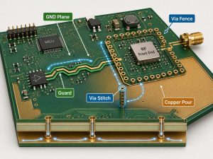
  • Ground via stitching
  • RF connector launch area
  • Shielding area
  • Tight trace control
  • Low-loss laminate
  • Stable reference plane

Project note:
For RF and microwave boards, the PCB is not only a carrier. It becomes part of the signal path.

PTFE Multilayer PCB Solutions for Complex High-Frequency Projects

Complex RF products often need more than a simple double-sided board. A multilayer PTFE structure can combine RF signal layers, ground planes, power layers, and control circuits.

Multilayer NeedWhat It Supports
RF Signal LayerControlled high-frequency routing
Ground PlaneBetter return path and shielding
Power LayerStable power distribution
Digital Control LayerSupports mixed RF and control functions
Via StitchingImproves grounding around RF areas
Hybrid Stack-UpBalances cost, RF performance, and strength

Commercial Benefits of PTFE Multilayer Support

Buyer ConcernMultilayer Solution
Board size is too largeMore routing layers reduce area
RF and digital circuits need separationLayer planning improves isolation
Signal path needs stable referenceGround planes support impedance
Product needs compact designMultilayer structure supports integration
Cost must stay controlledHybrid stack-up can help

Manufacturing Risks to Review

Risk AreaWhat the Manufacturer Should Check
Layer alignmentRegistration between RF and ground layers
LaminationBonding material and pressure control
DrillingHole quality in PTFE material
PlatingReliable copper in vias and holes
ImpedanceTrace width, dielectric height, and copper thickness
Hybrid structureCTE difference between PTFE and FR4

Best-Fit Projects

  • RF modules with dense routing
  • Antenna control boards
  • Radar electronics
  • Microwave communication boards
  • Mixed RF and digital products
  • Compact high-frequency assemblies

Buyer note:
A multilayer PTFE PCB needs strong front-end engineering review. It should not move directly from file upload to production without stack-up confirmation.

RF Connector Assembly Support for PTFE PCB Projects

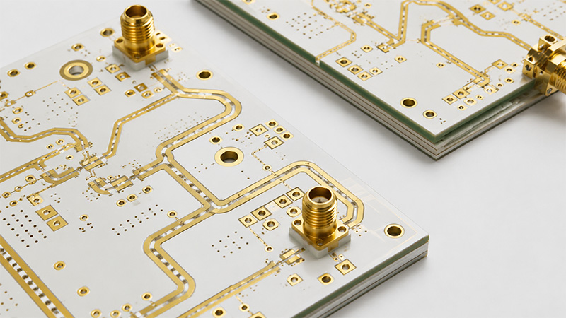
RF connectors affect both assembly quality and signal performance. For many high-frequency boards, the connector launch area decides how smoothly the signal enters or leaves the PCB.

RF Connector ItemWhat to CheckWhy It Matters
Connector TypeSMA, SMB, MMCX, U.FL, coaxial connectorMatches frequency, size, and cable interface
FootprintPad size, hole size, ground pad, solder mask openingSupports accurate assembly
Impedance TransitionConnector pin to RF traceReduces signal reflection
Ground Via StitchingVias near connector ground padsImproves return path
Mechanical SupportMounting holes, solder area, board edgeImproves connector strength
Soldering ControlTemperature, alignment, solder volumeSupports stable electrical and mechanical quality
InspectionVisual check, X-ray, continuity, RF test if requiredConfirms final assembly quality

RF Connector Launch Checklist

Design / Assembly PointRecommended Review
Center pin padMatch connector datasheet
Ground padsProvide enough solder area
Via placementKeep return path short
Trace transitionAvoid sudden width changes
Board edgeConfirm outline and connector position
Surface finishChoose finish suitable for soldering
Panel designSupport stable assembly handling

Business Value of Connector Assembly Support

  • Reduces mismatch between PCB design and assembly
  • Helps avoid weak solder joints
  • Improves RF signal transition
  • Supports one-stop PCB + PCBA supply
  • Reduces communication across suppliers
  • Makes prototype validation faster

Short takeaway:
RF connector assembly is not a small detail. It directly affects signal quality, board strength, and customer testing results.

DFM Review Support Before PTFE PCB Production

DFM review helps customers find production risks before fabrication starts. For PTFE PCB projects, this step is especially useful because high-frequency boards often have tight material and impedance requirements.

DFM Review ItemWhat EBest Circuit ChecksCustomer Benefit
Material MatchLaminate type, thickness, copper weightAvoids wrong material selection
Stack-UpLayer order, dielectric height, bonding materialSupports impedance and reliability
Trace Width / SpacingManufacturability and RF routing limitsReduces production risk
Impedance Target50-ohm or custom impedance requirementsImproves RF consistency
Via DesignHole size, annular ring, via placementSupports plating reliability
Copper BalanceCopper distribution across layersHelps board flatness
Surface FinishENIG or other finish optionsSupports soldering and contact quality
RF Connector AreaFootprint, launch, grounding, mechanical supportImproves assembly and signal transition
PanelizationPanel size, breakaway, handlingSupports smoother production

Typical Problems DFM Can Catch

ProblemPossible Impact
Trace width does not match impedance modelRF performance may shift
Via too close to RF traceSignal path may suffer
Connector pad does not match datasheetAssembly issue or weak solder joint
Copper area is unevenBoard flatness risk
Stack-up lacks clear reference planePoor signal return path
Material is hard to sourceLonger lead time

Files Needed for DFM Review

  • Gerber files
  • Drill files
  • Stack-up drawing
  • Impedance table
  • Material preference
  • BOM, if assembly is required
  • Connector datasheet
  • Special tolerance notes

Buyer note:
DFM review does not replace circuit design. It helps turn your design into a board that the factory can build with better control.

Why Choose EBest Circuit (Best Technology) for PTFE PCB Manufacturing?

Choosing a PTFE PCB supplier should not depend only on price. High-frequency boards need material knowledge, process control, engineering support, and assembly experience.

Customer NeedEBest Circuit Support
High-frequency PCB fabricationSupports PTFE and RF laminate projects
Material selection helpReviews Rogers, Taconic, Arlon, Nelco, and other options
Stack-up reviewChecks layer structure and impedance feasibility
Controlled impedanceSupports RF and high-speed requirements
DFM before productionHelps reduce manufacturing risks
RF connector assemblySupports footprint, grounding, soldering, and inspection review
PCBA assemblySupports SMT, through-hole, sourcing, and testing
Project stagesSupports prototype, small batch, and volume production
Global deliverySupports overseas customers with one-stop service

Why This Matters for Buyers

Buying ConcernHow One-Stop Support Helps
Too many suppliersPCB, sourcing, assembly, and testing can stay together
RF board has tight requirementsEngineering review starts before production
Material choice is unclearTeam can suggest workable options
Assembly needs RF connectorsPCB and PCBA teams can align early
Prototype schedule is tightEarly review helps reduce redesign delays
Project may move to batch productionProcess records support repeat orders

Good Projects to Discuss with EBest Circuit

  • RF PCB fabrication
  • PTFE PCB prototype
  • Rogers-based high-frequency board
  • Antenna PCB
  • Microwave PCB
  • Multilayer RF PCB
  • RF connector assembly
  • Turnkey PCBA for high-frequency products

Request a Quote

To get a faster and more accurate quotation, send:

Required InformationHelpful Details
Gerber filesRequired for PCB quotation
Stack-upNeeded for impedance and layer review
Material requestRogers, PTFE, Taconic, Arlon, Nelco, or equivalent
QuantityPrototype, small batch, or volume
Surface finishENIG, immersion silver, or other options
BOMRequired for PCBA quotation
Pick-and-Place fileRequired for SMT assembly
Testing requirementElectrical test, AOI, X-ray, functional test, RF test if needed

For PTFE PCB fabrication or turnkey assembly support, contact: sales@bestpcbs.com

FAQs About PTFE PCB Manufacturing

QuestionAnswer
Is PTFE PCB better than FR4?PTFE performs better in RF, microwave, and low-loss applications. FR4 still works well for many standard electronics.
What applications need PTFE PCB?RF modules, antenna boards, microwave circuits, radar electronics, satellite communication, and wireless equipment often need it.
Can PTFE PCB support multilayer designs?Yes. It can support multilayer and hybrid stack-ups when the manufacturer controls lamination, drilling, plating, and impedance.
Can EBest Circuit support PTFE PCB assembly?Yes. EBest Circuit supports PCB fabrication, component sourcing, SMT assembly, through-hole assembly, testing, and delivery.
What files should I send for a quote?Send Gerber files, drill files, stack-up, material request, impedance requirement, quantity, and drawings. For assembly, send BOM and Pick-and-Place files.
Can PTFE PCB use RF connectors?Yes. RF connectors such as SMA, SMB, MMCX, U.FL, and coaxial types can be assembled when the footprint and grounding design match the connector requirement.
Why does PTFE PCB cost more than FR4?PTFE laminate costs more. The manufacturing process also needs tighter drilling, plating, lamination, and impedance control.
Can I use Rogers material for PTFE PCB?Yes. Rogers offers high-frequency materials for RF and microwave products. The right choice depends on frequency, loss target, stack-up, and budget.
Does DFM review help before production?Yes. It can catch stack-up, impedance, via, connector, copper balance, and manufacturability issues before fabrication.
Can PTFE PCB support prototype and batch production?Yes. A capable manufacturer can support samples first, then help move the project to small-batch or volume production.

Final Takeaway

If You Need…Focus On…
Stable RF signalPTFE laminate, impedance, copper control
Reliable productionDFM review, drilling, plating, lamination
Compact RF designMultilayer or hybrid stack-up
Complete assemblyRF connector support, SMT, testing
Fewer supplier issuesOne-stop PCB + PCBA service
Faster quotationComplete Gerber, stack-up, BOM, and requirement files

PTFE PCB manufacturing is a project-level decision, not just a material choice. Buyers should check the laminate, stack-up, impedance, RF connector design, DFM support, assembly plan, and supplier capability before production.

EBest Circuit (Best Technology) helps customers move from RF board design files to reliable PCB fabrication and PCBA assembly with practical engineering support.

You may also like

PTFE PCB Guide: Materials, Benefits, and Applications
Tuesday, May 19th, 2026

PTFE PCB plays an important role in RF, microwave, antenna, radar, and high-frequency communication products. Engineers choose PTFE-based circuit boards when they need low signal loss, stable impedance, and reliable high-frequency performance. Compared with standard FR4, PTFE materials offer better electrical stability at higher frequencies. However, material choice alone does not decide the final result. The stack-up, copper design, layout, drilling, plating, surface finish, and manufacturing control also matter. This guide explains what a PTFE PCB is, how PTFE laminate works, what layout factors need attention, and how to choose the right PTFE PCB manufacturer for your project.

PTFE PCB

What Is a PTFE PCB?

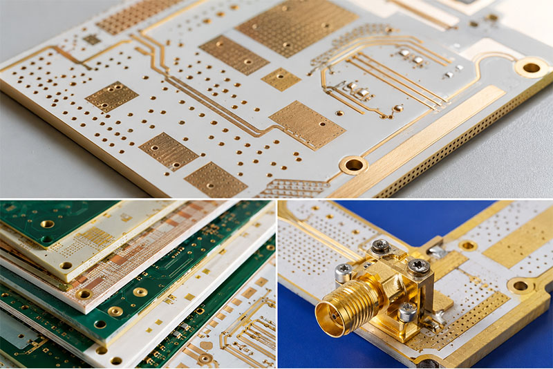
A PTFE PCB is a printed circuit board made with PTFE-based dielectric material. PTFE stands for polytetrafluoroethylene. It has low signal loss, low moisture absorption, strong chemical resistance, and stable electrical behavior.

Engineers often use PTFE boards in RF and microwave circuits. These circuits need better signal control than standard electronic boards. For example, antenna modules, radar boards, satellite communication products, RF amplifiers, and microwave devices often need PTFE materials.

A PTFE board may have one layer, two layers, or many layers. Some projects use pure PTFE laminate. Others combine PTFE with FR4 or other high-frequency materials. This hybrid structure can balance performance, cost, and strength.

PTFE behaves differently from FR4 during fabrication. It needs careful drilling, hole treatment, plating, lamination, and surface preparation. For this reason, a PTFE board requires more process control than a common FR4 board.

In simple terms, PTFE PCB is not just a board with a special material. It is a high-frequency circuit platform. Material, layout, stack-up, and manufacturing process must work together.

Why Do Engineers Use PTFE PCB Material in High-Frequency Circuits?

Engineers use PTFE PCB material because it helps high-frequency signals travel with less loss. At RF and microwave frequencies, the PCB trace acts like a transmission line. Small changes in material or trace shape can affect the signal.

PTFE material offers several key benefits:

  • Low dielectric constant
  • Low dissipation factor
  • Stable signal speed
  • Low moisture absorption
  • Good chemical resistance
  • Strong RF and microwave performance

These features help reduce signal loss. They also help keep impedance more stable. This matters in RF modules, antennas, filters, couplers, radar systems, and communication products.

FR4 works well for many standard electronic products. But it has higher loss at high frequencies. When a product needs cleaner signal transfer, PTFE becomes a better option.

Still, the material does not solve every problem. The layout must match the target impedance. The stack-up must match the design model. The copper thickness, dielectric thickness, via design, and surface finish also affect the final result.

That is why engineers should confirm the material and stack-up before production. Early review can save time and reduce design changes later.

PTFE PCB Laminate: Which Properties Matter Most?

A PTFE PCB laminate should match both electrical and production needs. Many buyers only check the dielectric constant. That is not enough. A good material choice needs a wider review.

PropertyWhy It Matters
Dielectric ConstantAffects impedance and signal speed
Dissipation FactorAffects signal loss
Laminate ThicknessHelps control impedance
Copper RoughnessAffects conductor loss at high frequency
Thermal ConductivityHelps manage heat
Dimensional StabilitySupports accurate layer alignment
Peel StrengthHelps copper stay bonded
Moisture AbsorptionHelps keep electrical values stable
Copper WeightAffects current, loss, and etching control

For RF circuits, dielectric constant and dissipation factor matter most. But copper roughness also plays a big role. At high frequencies, the signal travels near the copper surface. Rough copper can increase loss.

Laminate thickness also needs attention. If the thickness changes too much, impedance can shift. This may affect RF performance.

Before production, customers should confirm the laminate brand, thickness, copper weight, surface finish, and tolerance requirements. For multilayer boards, bonding material also matters.

A good PTFE PCB manufacturer should help review these details. The goal is simple: match the material with the real design and the real production process.

PTFE Teflon PCB vs FR4 PCB: What Is the Difference?

Many people use the term PTFE Teflon PCB when they talk about PTFE-based boards. Teflon is a well-known trade name. PTFE is the material name. In PCB projects, both terms often point to the same type of high-frequency board.

The main difference between PTFE and FR4 is electrical performance. FR4 works well for many common circuit boards. It offers good strength and a lower cost. PTFE offers better signal performance at high frequencies.

ItemPTFE Teflon PCBFR4 PCB
Main UseRF and microwave circuitsGeneral electronics
Signal LossLowerHigher at high frequency
Impedance StabilityBetter for RF designsGood for standard boards
CostHigherLower
Processing DifficultyHigherLower
Typical ProductsAntenna, radar, RF module, microwave boardControl board, power board, consumer electronics

You do not need PTFE for every board. If the product works at low speed or low frequency, FR4 may perform well. If the product works in RF or microwave bands, PTFE can give better results.

Some projects use both materials in one board. For example, the RF layer may use PTFE. Other layers may use FR4. This design can reduce cost while keeping RF performance where it matters.

The right choice depends on the frequency, signal loss target, cost target, board structure, and production volume.

How Does a High Frequency PCB with PTFE Improve Signal Performance?

A high frequency PCB with PTFE can improve signal performance by reducing loss and supporting stable impedance. In RF circuits, the board material becomes part of the circuit. The signal does not only travel through copper. It also interacts with the dielectric material around the trace.

PTFE helps in several ways.

First, it has a low dissipation factor. This reduces signal loss. It helps RF signals travel farther with less drop.

Second, it offers stable dielectric behavior. This helps engineers design accurate microstrip, stripline, and coplanar waveguide structures.

Third, it supports better phase stability. This matters in antennas, radar systems, and microwave communication products.

Fourth, it absorbs little moisture. This helps the board keep stable electrical behavior in changing environments.

However, PTFE does not work alone. The manufacturer must also control the board structure. Trace width, copper thickness, dielectric thickness, via position, solder mask, and plating thickness all affect the final result.

For example, a 50-ohm RF trace needs the right width and dielectric height. If the board thickness changes, impedance may shift. If copper plating becomes too thick, the trace shape may also change.

So, high-frequency PCB performance needs both good material and good manufacturing control.

How Should PTFE PCB Layout Be Designed for Stable High-Frequency Performance?

PTFE PCB layout should focus on signal path control, impedance stability, return path quality, and manufacturing feasibility. In many projects, the customer already has the circuit design. The PCB manufacturer mainly helps review the layout from a fabrication and DFM view.

Here are the key layout points.

Controlled Impedance

RF traces often need a clear impedance target, such as 50 ohms. The trace width, copper thickness, dielectric thickness, and ground plane all affect impedance. Before fabrication, the manufacturer should check whether the stack-up can meet the required value.

Short and Clean RF Paths

RF paths should stay as short and direct as possible. Sharp corners, sudden width changes, and long detours can affect signal quality. Smooth trace transitions help support stable performance.

Good Ground Reference

A stable ground plane helps the signal return path. RF layouts often need via stitching near signal paths, connectors, shielding areas, and ground edges. This helps reduce noise and improve RF behavior.

Proper Via Design

Vias affect high-frequency signals. Layout engineers should place RF vias carefully. Ground vias should support the return current path. Signal vias should avoid unnecessary length where possible.

Trace Width and Spacing

PTFE material needs careful process control. Very fine traces and tight spacing should match the manufacturer’s capability. A DFM review can confirm whether the design fits real production limits.

Copper Balance

Copper balance helps control board flatness and lamination behavior. This matters more in PTFE multilayer boards. Uneven copper can make production harder.

RF Connector Footprints

RF connectors need accurate pad size, ground pads, and solder mask clearance. A small footprint issue can affect both assembly and RF performance.

DFM Review Before Fabrication

A strong DFM review can check trace width, spacing, annular ring, via size, impedance stack-up, copper balance, panel design, and surface finish. This step helps turn layout data into a stable physical board.

For EBest Circuit, layout support mainly focuses on manufacturability, stack-up review, impedance feasibility, and production optimization. This helps customers improve the board before fabrication starts.

Rogers PTFE PCB: When Should You Choose Rogers-Based Materials?

A Rogers PTFE PCB can support RF and microwave products that need stable material quality. Rogers offers many high-frequency laminates. Some use PTFE-based systems, while others use different advanced resin systems.

Engineers often choose Rogers materials for:

  • RF modules
  • Microwave boards
  • Antenna circuits
  • Radar systems
  • Satellite communication products
  • Wireless infrastructure
  • High-speed test equipment

Rogers materials can offer low loss, stable dielectric values, and strong documentation. These features help engineers build more predictable RF products.

But Rogers is not the only option. Some projects may use Taconic, Isola, Panasonic, or other high-frequency materials. The best choice depends on the real application.

Before choosing a Rogers material, check these points:

  • Operating frequency
  • Target impedance
  • Board thickness
  • Copper weight
  • Loss requirement
  • Thermal demand
  • Layer count
  • Surface finish
  • Prototype or mass production plan

A good supplier should not simply suggest the most expensive material. Instead, the supplier should help match the material with performance, cost, and delivery needs.

For many projects, the best material is not the highest-grade material. It is the material that fits the design target and production plan.

Can PTFE Multilayer PCB Support Complex RF Designs?

Yes, PTFE multilayer PCB can support complex RF designs. It can combine RF signal layers, ground planes, power layers, control circuits, and shielding structures in one board.

This structure helps reduce board size. It also improves grounding and signal routing. Many RF modules, antenna systems, radar boards, and communication products use multilayer structures.

A typical PTFE multilayer board may include:

  • RF signal layers
  • Solid ground planes
  • Power layers
  • Digital control layers
  • Shielding areas
  • Via stitching
  • Hybrid PTFE and FR4 layers

Multilayer PTFE boards need strong process control. PTFE is softer than FR4. It also behaves differently during drilling and lamination. The manufacturer must control drilling, hole treatment, plating, bonding, and layer alignment carefully.

Hybrid stack-ups also need extra review. PTFE and FR4 do not expand in the same way under heat. The stack-up should account for this difference.

For RF products, the layer structure must also support impedance control. The distance between signal trace and reference plane must stay consistent. Copper thickness and dielectric thickness must match the design target.

Before production, customers should share the Gerber files, stack-up, impedance requirements, material choice, and special tolerance needs. This helps the manufacturer review the project clearly.

A PTFE multilayer PCB can work very well when design and production teams align early.

What Should Be Considered for RF Connector Assembly on PTFE PCB?

RF connectors play an important role in PTFE PCB performance. In many RF and microwave boards, the connector is not just a mechanical part. It is also the starting point of the signal path. If the connector footprint, soldering, grounding, or impedance transition is not well controlled, the board may lose part of its high-frequency advantage.

Connector Footprint Accuracy

The RF connector footprint should match the connector datasheet. Pad size, hole size, mounting position, solder mask opening, and ground pad layout all need careful review. For SMA, SMB, MMCX, or other coaxial connectors, even a small footprint error may affect assembly strength and RF performance.

50-Ohm Impedance Transition

Many RF connectors work with a 50-ohm transmission line. The transition from the connector pin to the PCB trace should stay smooth and controlled. Sudden trace width changes, long stubs, or poor pad geometry can create signal reflection. For PTFE PCB, the trace width should match the material thickness, copper thickness, and dielectric constant.

Ground Via Stitching

Good grounding helps the connector perform well. Ground vias should be placed close to the connector ground pads and around the RF launch area. This creates a shorter return path and helps reduce noise, radiation, and signal leakage.

Mechanical Stability

RF connectors often face repeated mating, cable pulling, and vibration. The PCB layout should provide enough copper area, mounting holes, and solder support. For heavier connectors, mechanical reinforcement may be needed to protect the solder joints and board edge.

Soldering Quality

PTFE PCB materials behave differently from FR4 during heating. The assembly process should control the soldering temperature, dwell time, and connector alignment. Clean solder joints help maintain both electrical performance and mechanical strength.

Board Edge and Connector Alignment

Many RF connectors mount at the board edge. The board outline, edge plating, connector position, and panel design should match the assembly requirement. Good alignment helps the cable connect smoothly and reduces mechanical stress.

Inspection After Assembly

After RF connector assembly, the board should be checked for solder quality, connector position, grounding, and mechanical strength. For high-frequency products, visual inspection, X-ray inspection, continuity testing, and RF-related testing may also be required based on the project.

In short, RF connector assembly on PTFE PCB requires close control of both layout and manufacturing details. A good PTFE PCB manufacturer should review the connector footprint, impedance transition, grounding method, soldering process, and inspection plan before production. This helps the final board keep stable RF performance after assembly.

PTFE PCB Manufacturing Capabilities at EBest Circuit (Best Technology)

PTFE PCB manufacturing needs stable material control, precise drilling, reliable plating, and strong impedance management. EBest Circuit (Best Technology) supports PTFE PCB fabrication, DFM review, PCBA assembly, component sourcing, testing, and turnkey electronics manufacturing for RF, microwave, antenna, radar, and communication applications.

CapabilityTechnical SpecificationBusiness Benefit
Material CoveragePTFE, Rogers, Taconic, Arlon, Nelco, and other RF laminatesMore choices for RF, microwave, antenna, and radar boards
Manufacturing Precision1–50 layers, 0.4–6.0 mm board thickness, 0.10 mm laser drilling, controlled impedance supportBetter signal stability and lower production risk
Quality CertificationsISO9001, ISO13485, IATF16949, AS9100D quality system supportSuitable for demanding industrial and regulated projects
Turnaround TimePrototype, small-batch, and volume production supportFaster project validation and smoother production planning
Global Sourcing & DeliveryPCB fabrication, component sourcing, PCBA assembly, testing, and deliveryLess supplier coordination and easier project management

Before production, EBest Circuit can review the material, stack-up, impedance target, trace width, via design, copper thickness, surface finish, and assembly needs. This helps customers reduce design-to-production risks and keep RF performance more stable.

For PTFE PCB projects, the goal is not only to manufacture the board. The goal is to keep the RF signal path stable from layout to final assembly. With DFM support, high-frequency PCB experience, and one-stop PCB/PCBA service, EBest Circuit helps customers move from prototype to reliable production.

Why Choose EBest Circuit (Best Technology) as Your PTFE PCB Manufacturer?

Choosing the right PTFE PCB manufacturer matters because PTFE boards need tighter process control than standard FR4 boards. The supplier should understand high-frequency materials, stack-up control, impedance, drilling, plating, and DFM review.

EBest Circuit (Best Technology) supports PCB fabrication, PCBA assembly, component sourcing, DFM review, testing, and turnkey electronics manufacturing. For PTFE and high-frequency PCB projects, the team can help review material choice, stack-up, impedance targets, layout feasibility, and production details.

Here are the main advantages.

High-Frequency PCB Experience

EBest Circuit works with high-frequency PCB materials for RF, microwave, antenna, communication, industrial control, automotive electronics, aerospace/UAV, and other electronic products.

DFM Review Before Production

The engineering team can review Gerber files, stack-up, trace width, spacing, via design, copper balance, impedance needs, and panel layout. This helps customers find possible issues before fabrication.

Controlled Impedance Support

Many PTFE boards need controlled impedance. EBest Circuit can help check the stack-up and production feasibility based on the target impedance.

PCB Fabrication and PCBA Assembly

Some customers need bare boards only. Others need complete assembly. EBest Circuit can support PCB fabrication, component sourcing, SMT assembly, through-hole assembly, testing, and box-build assembly.

Prototype to Batch Production

Many high-frequency projects start with samples. After testing, they move to small batch or volume production. EBest Circuit can support different stages with stable process control.

Quality and Traceability

EBest Circuit focuses on quality control, process records, and production traceability. This helps customers in industries that need stable documentation and reliable manufacturing support.

Clear Engineering Communication

High-frequency boards need clear communication. Small details can affect the final result. The team can discuss material, stack-up, tolerance, surface finish, assembly needs, and delivery plan with customers before production.

If you need PTFE PCB fabrication or turnkey assembly support, you can send Gerber files, stack-up, BOM, drawings, and technical requirements to sales@bestpcbs.com for review and quotation.
To summarize‌, a PTFE PCB is a strong choice for RF, microwave, antenna, radar, and high-frequency communication products. It helps reduce signal loss and supports stable electrical performance.

Still, the final result depends on more than material. The layout, stack-up, copper design, drilling, plating, surface finish, and assembly process all matter.

For high-frequency projects, an experienced PTFE PCB manufacturer can help make the process smoother. With early material review, layout checking, DFM support, and controlled fabrication, customers can move from prototype to production with more confidence.

FAQs About PTFE PCB

Q1: Is PTFE PCB only for RF circuits?
A1: PTFE PCB mainly serves RF, microwave, antenna, radar, and communication circuits. Some high-speed or low-loss products also use PTFE materials.

Q2: Is PTFE always better than FR4?
A2: No. PTFE works better for high-frequency and low-loss circuits. FR4 still works well for many standard electronic products. The best choice depends on frequency, cost, structure, and performance goals.

Q3: What files should I send for a PTFE PCB quote?
A3: You can send Gerber files, drill files, stack-up, board thickness, copper weight, surface finish, impedance needs, quantity, and special tolerance requirements. If you need assembly, also send the BOM and Pick-and-Place files.

Q4: Can PTFE PCB support SMT assembly?
A4: Yes. PTFE boards can support SMT assembly. The process should consider board thickness, material behavior, component type, soldering profile, and panel handling.

Q5: Which surface finish works well for PTFE PCB?
A5: ENIG often works well because it gives a flat and solderable surface. Other finishes may also fit some projects, depending on soldering, bonding, cost, and product needs.

Q6: Why does PTFE PCB cost more than FR4 PCB?
A6: PTFE materials cost more. The production process also needs tighter control. Drilling, hole treatment, plating, lamination, and impedance control all require more care.

Q7: Can PTFE work with FR4 in one board?
A7: Yes. Many designs use PTFE and FR4 together. This hybrid stack-up can balance RF performance, strength, board thickness, and cost.

Q8: How can I reduce risk before production?
A8: Confirm the material, stack-up, impedance target, copper thickness, via design, surface finish, and layout details early. A DFM review can help find issues before fabrication.
You may also like

Top 10 RF PCB Manufacturers in USA | Trusted RF PCB Manufacturer Guide
Friday, December 19th, 2025

Choosing the right RF PCB manufacturer in the USA directly affects signal integrity, insertion loss, and long-term product reliability. In RF systems operating above 1 GHz, even a ±5% variation in dielectric constant (Dk) or ±1 mil trace deviation can cause impedance mismatch and measurable signal degradation.
For applications such as 5G base stations, radar modules, satellite communication, medical imaging, and defense electronics, RF PCBs demand more than standard multilayer fabrication. This guide reviews the top 10 RF PCB manufacturers in the USA, explains how they were evaluated, and helps buyers identify what truly defines a capable RF PCB manufacturing partner.

Top 10 RF PCB Manufacturers in USA | Trusted RF PCB Manufacturer Guide  https://www.bestpcbs.com/blog/2025/12/top-10-rf-pcb-manufacturers-in-usa/

What Is an RF PCB Manufacturer?

An RF PCB manufacturer is a factory equipped to control high-frequency electrical behavior, not just fabricate boards using RF laminates.

A qualified RF PCB manufacturer typically demonstrates:

  • Controlled impedance tolerance of ±5–10%
  • Proven experience with Rogers, Taconic, PTFE, and hybrid RF stack-ups
  • Line width and spacing control down to ±1 mil
  • RF-aware stack-up and grounding validation
  • Process consistency between prototype and volume production

Unlike standard digital PCBs, RF designs are sensitive to copper roughness, resin distribution, and prepreg variation. Manufacturers without RF-specific process control often struggle to deliver repeatable RF performance.
Common Challenges When Choosing an RF PCB Manufacturer in the USA

Despite the strong PCB ecosystem in the USA, RF buyers frequently encounter the following issues:

  • Impedance drift between batches, especially in volume production
  • Limited experience with hybrid RF stack-ups (Rogers + FR-4)
  • RF performance verified only at prototype stage, not scaled production
  • Long RF laminate lead times (often 4–6 weeks)
  • Minimal engineering feedback beyond Gerber fabrication

According to industry feedback, over 30% of RF PCB project delays are caused by material handling or impedance inconsistencies rather than design errors. This highlights why RF capability must be validated beyond certifications.

Common Challenges When Choosing an RF PCB Manufacturer in the USA https://www.bestpcbs.com/blog/2025/12/top-10-rf-pcb-manufacturers-in-usa/

How We Evaluated the Top RF PCB Manufacturers in the USA?

Manufacturers were evaluated using practical RF manufacturing benchmarks, not marketing claims.

Key evaluation criteria included:

  • RF material portfolio (Rogers RO4350B, RO4003C, RO5880, Taconic, PTFE)
  • Demonstrated impedance control capability (≀ ±10%)
  • Experience with multilayer RF and mixed-signal designs
  • Quality certifications relevant to RF applications
  • Ability to support prototype + mid-volume production

Factories focusing only on RF prototyping without scalable production control were ranked lower.

Top 10 RF PCB Manufacturers in USA

RankCompany NameRF PCB CapabilityKey AdvantagesLocation
1TTM TechnologiesRF & microwave multilayersDefense & aerospace expertiseCalifornia
2SanminaHigh-reliability RF PCBsEnd-to-end manufacturingCalifornia
3Summit InterconnectRF multilayer & HDIQuick-turn RF capabilityCalifornia
4Advanced CircuitsRF prototypesFast turnaroundColorado
5Sierra CircuitsHigh-frequency fabricationStrong DFM supportCalifornia
6Rush PCBRF proto & low volumeCost efficiencyCalifornia
7Epec Engineered TechnologiesRF & mixed-signal PCBsIntegrated PCBAMassachusetts
8Green CircuitsRF PCB manufacturingEMS integrationCalifornia
9All Flex SolutionsRF flexible circuitsSpecialty RF flexMinnesota
10APCTComplex RF multilayersAdvanced stack-upsCalifornia

Are US RF PCB Manufacturers Always the Best Choice?

US RF PCB manufacturers offer clear advantages:

  • Local engineering communication
  • ITAR and defense compliance
  • Established aerospace and telecom experience

However, buyers should also consider:

  • Higher manufacturing costs (often 30–50% above offshore)
  • Limited RF laminate inventory
  • Less flexibility for mid-volume scaling

As a result, many OEMs now adopt a hybrid sourcing strategy, using US suppliers for early development and qualified offshore RF PCB manufacturers for volume production.
US RF PCB Manufacturers 
https://www.bestpcbs.com/blog/2025/12/top-10-rf-pcb-manufacturers-in-usa/

Global Alternative RF PCB Manufacturer for USA Customers

As RF projects become more globalized, many USA companies now evaluate global RF PCB manufacturers that offer comparable RF performance with better lead time, cost flexibility, and material availability. Below is a representative list of global RF PCB manufacturers serving high-frequency and microwave applications, based on manufacturing capability, RF material experience, and export readiness.
RankCompany NameCountry / RegionRF PCB CapabilityKey Strengths for USA Customers
1EBest Circuit (Best Technology)China / VietnamRF, microwave, hybrid stack-upsFast lead time, wide RF materials, 30–50% cost advantage
2AT&SAustriaRF, high-frequency, IC substratesHigh-end RF technology, EU quality standards
3UnimicronTaiwanRF, HDI, high-speedAdvanced multilayer RF capability
4CompeqTaiwanRF & high-speed PCBsStable mass production for RF designs
5Meiko ElectronicsJapanRF & automotive PCBsHigh reliability, automotive RF experience
6Shennan CircuitsChinaRF & telecom PCBsStrong telecom and RF infrastructure
7IbidenJapanRF & package substratesPrecision RF manufacturing
8KinwongChinaRF & mixed-signal PCBsCost-effective RF volume production
9Chin Poon IndustrialThailandRF & automotive PCBsSoutheast Asia manufacturing flexibility
10Dynamic ElectronicsTaiwanRF multilayer PCBsMature RF fabrication processes

Why Global Buyers Choose EBest Circuit (Best Technology) as an Experienced RF PCB Manufacturer?

EBest Circuit (Best Technology) supports RF PCB programs with a focus on repeatability and manufacturability, not just RF materials.

Our RF PCB capability includes:

  • Rogers, Taconic, Isola, and hybrid RF stack-ups
  • Controlled impedance down to ±8%
  • RF trace width control to ±1 mil
  • Multilayer RF boards up to 20+ layers
  • ISO 9001, ISO 13485, IATF 16949, and AS9100D certified systems
  • MES-based traceability for materials and process control

This enables USA customers to transition smoothly from prototype to volume production without RF performance drift.

FAQs

1. What materials do RF PCB manufacturers typically use?

Common materials include Rogers RO4000/RO5000 series, Taconic, PTFE, and selected low-loss FR-4.

2. Is FR-4 suitable for RF PCB applications?

FR-4 is generally suitable below 1 GHz; higher frequencies benefit from low-loss laminates.

3. How do RF PCB manufacturers control impedance?

Through stack-up modeling, dielectric thickness control, copper roughness management, and process calibration.

4. What is the typical lead time for RF PCB prototypes?

Most RF PCB prototypes ship within 7–12 working days, depending on material availability.

5. How can I verify an RF PCB manufacturer’s RF capability?

Review impedance data, RF material history, similar project experience, and quality certifications.

You may also like

RF PCB Manufacturer: Complete Guide to Materials and Design Considerations
Thursday, December 18th, 2025

An RF PCB manufacturer specializes in the design and fabrication of printed circuit boards used in radio-frequency, microwave, and high-frequency electronic systems. As operating frequencies increase, PCB performance is no longer determined only by connectivity, but by electromagnetic behavior, material stability, and manufacturing precision.

This pillar page provides a comprehensive, engineering-focused overview of RF PCB manufacturing. It covers what an RF PCB manufacturer does, how RF PCBs differ from standard boards, RF frequency definitions, materials, stackup design, manufacturing processes, common mistakes, and how to evaluate RF PCB manufacturing capability.

What Is an RF PCB Manufacturer?

An RF PCB manufacturer is a PCB supplier with specialized expertise in producing circuit boards for applications operating at radio frequencies, typically above 30 MHz. At these frequencies, PCB traces act as transmission lines, and small variations in geometry or material properties can significantly affect signal integrity.

Compared with standard PCB manufacturers, RF PCB manufacturers must control:

  • Dielectric constant (Dk) stability across frequency and temperature
  • Dissipation factor (Df) to minimize insertion loss
  • Tight impedance tolerance, often ±5% or better
  • Copper surface roughness, which directly affects high-frequency loss
  • Stackup symmetry and lamination consistency

These requirements mean RF PCB manufacturing is as much an electromagnetic discipline as a mechanical one.

What Is an RF PCB Manufacturer?   https://www.bestpcbs.com/blog/2025/12/rf-pcb-manufacturer/

What Is an RF PCB Manufacturer?

RF PCB vs Standard PCB (Quick Comparison)

Although RF PCBs and standard PCBs may look similar in appearance, they are fundamentally different in design philosophy, material selection, and manufacturing control. As frequency increases, even small variations that are acceptable in standard PCBs can cause severe performance degradation in RF designs.

Key Differences Between RF PCB and Standard PCB

Comparison ItemRF PCBStandard PCB
Typical operating frequency>30 MHz up to GHz/mmWaveDC to low-speed digital
Signal behaviorTransmission-line dominatedLumped-circuit dominated
Primary design concernImpedance, loss, phase stabilityConnectivity and routing
Core materialsRogers, PTFE, Taconic, RF laminatesFR-4
Dielectric constant (Dk)Tightly controlled, frequency-stableWider tolerance
Dissipation factor (Df)Low-loss requiredLess critical
Copper surface roughnessStrictly controlledUsually not critical
Impedance tolerance±5% or tighter±10% common
Stackup complexityHigh, often hybridRelatively simple
Manufacturing difficultyHighModerate
Cost sensitivityPerformance-drivenCost-driven

In short, standard PCB manufacturing prioritizes manufacturability and cost, while RF PCB manufacturing prioritizes electrical performance and consistency. This is why RF PCBs must be produced by a qualified RF PCB manufacturer rather than a general PCB supplier.

What Frequency Range Is Considered RF in PCB Manufacturing?

In PCB manufacturing, RF generally refers to frequencies above 30 MHz, where wavelength becomes comparable to trace dimensions and transmission-line effects dominate.

Typical frequency classifications include:

  • 30 MHz – 300 MHz: VHF
  • 300 MHz – 3 GHz: UHF and microwave
  • 3 GHz – 30 GHz: Microwave and millimeter-wave

As frequency increases, the impact of dielectric variation, copper roughness, and impedance mismatch becomes more severe, requiring stricter manufacturing controls.

RF PCB Frequency Range https://www.bestpcbs.com/blog/2025/12/rf-pcb-manufacturer/

Common RF PCB Materials

Material selection is one of the most important responsibilities of an RF PCB manufacturer. RF materials are chosen for predictable dielectric behavior and low signal loss across frequency.

Typical RF PCB Materials

  • Rogers RO4003C / RO4350B – Widely used RF laminates with stable Dk
  • Rogers RO3003 / RO3006 – Microwave and millimeter-wave applications
  • Taconic RF materials – Cost-effective RF solutions
  • PTFE-based laminates – Ultra-low loss for high-frequency designs

A qualified RF PCB manufacturer evaluates materials based on frequency range, insertion loss targets, thermal performance, and manufacturability.

RF PCB Applications

RF PCBs are used in applications where signal integrity at high frequency is critical.

Common RF PCB applications include:

  • 5G and cellular base stations
  • RF front-end modules and power amplifiers
  • Automotive radar systems (24 GHz, 77 GHz)
  • Satellite and aerospace communication systems
  • Wireless IoT, Wi-Fi, and Bluetooth modules

Each application places different requirements on materials, stackup, and manufacturing precision.

RF PCB Manufacturing Process (Simplified)

RF PCB manufacturing requires tighter process control than standard PCB fabrication.

A simplified RF PCB manufacturing flow includes:

RF PCB Manufacturing Process  https://www.bestpcbs.com/blog/2025/12/rf-pcb-manufacturer/

1. RF laminate handling and moisture control

2. Precision drilling to prevent dielectric deformation

3. Copper etching with controlled surface roughness

4. Sequential lamination for hybrid RF/FR-4 stackups

5. Impedance-controlled trace patterning

6. Electrical testing and impedance verification

Consistency across batches is critical, as even small process variations can affect RF performance.

RF PCB Stackup Design Considerations

Stackup design directly influences impedance stability, loss, and manufacturability.

Key stackup considerations RF PCB manufacturers must control include:

  • Uniform dielectric thickness
  • Stable Dk across all RF layers
  • Continuous and uninterrupted reference planes
  • Compatibility between RF laminates and FR-4 prepregs
  • Controlled lamination sequence to avoid warpage

In many cases, RF PCB manufacturers collaborate with customers to finalize stackups before production.

Common RF PCB Manufacturing Mistakes

RF PCBs are highly sensitive to manufacturing errors.

Common RF PCB manufacturing mistakes include:

  • Using inappropriate materials for the target frequency
  • Ignoring copper roughness effects on insertion loss
  • Poor stackup symmetry causing mechanical distortion
  • Etching variation leading to impedance mismatch
  • Lack of RF-specific design-for-manufacturing review

Experienced RF PCB manufacturers reduce these risks through upfront engineering validation and strict process control.

Why Choose EBest Circuit (Best Technology) as Your RF PCB Manufacturer?

When evaluating RF PCB manufacturing capability, EBest Circuit (Best Technology) is often selected due to its strong focus on RF and high-frequency PCB production. With experience in RF materials, controlled impedance manufacturing, and RF-focused engineering support, EBest Circuit (Best Technology) demonstrates the core capabilities expected from a professional RF PCB manufacturer.

By choosing EBest Circuit (Best Technology), customers benefit from:

  • Proven RF and microwave PCB manufacturing experience
  • Tight impedance and material control
  • Engineering-driven process validation
  • Reliable performance for high-frequency applications

For projects involving RF, microwave, or high-speed communication systems, selecting EBest Circuit (Best Technology) as your RF PCB manufacturer helps reduce technical risk and improve overall product reliability.

FAQs About RF PCB Manufacturing

1. What does an RF PCB manufacturer do?

    An RF PCB manufacturer produces printed circuit boards optimized for high-frequency performance, focusing on impedance control, low signal loss, and material stability.

    2. Can FR-4 be used in RF PCB manufacturing?

    FR-4 may be acceptable for low-frequency RF designs, but at higher frequencies it suffers from higher loss and unstable dielectric properties.

    3. Why are RF PCBs more difficult to manufacture?

    RF PCBs are sensitive to small variations in materials, geometry, and processing, making manufacturing control critical.

    4. Are RF PCBs more expensive than standard PCBs?

    RF PCBs typically cost more due to specialized materials, tighter tolerances, and additional process controls.

    You may also like

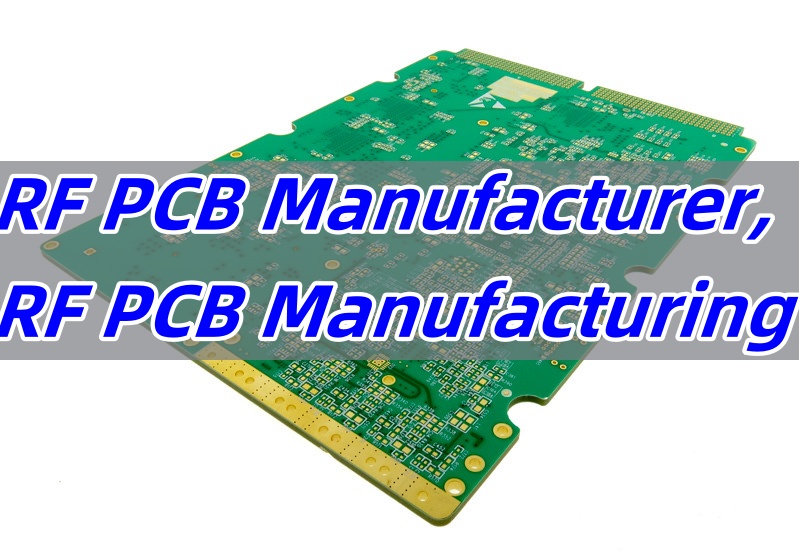
    RF PCB Manufacturer, RF PCB Manufacturing​
    Monday, April 7th, 2025

    RF PCB manufacturer is a term often searched by engineers and businesses looking for high-quality, high-frequency printed circuit boards. In today’s fast-paced tech world, signal strength, low loss, and stable performance are non-negotiable. Whether you are creating 5G devices or aerospace modules, having the right partner in RF PCB fabrication is crucial. Let’s explore what goes into this process, how materials matter, and why the manufacturer you choose make a difference.

    EBest Circuit (Best Technology) is one of the leading RF PCB manufacturers in China, specializing in RF PCB fabrication, RF PCB design, and multilayer RF PCB manufacturing. EBest Circuit (Best Technology) used high-quality RF PCB materials, such as Rogers RO4350, RO4003, and PTFE (DuPont Teflon). We believe quality is the first. If you are looking for a reliable RF PCB manufacturer, just don’t hesitate to choose EBest Circuit (Best Technology) as your partner. Feel free to contact us at sales@bestpcbs.com.

    RF PCB Manufacturer, RF PCB Manufacturing​

    What is RF PCB Manufacturing?

    RF PCB manufacturing refers to the process of building circuit boards that handle high-frequency signals. Unlike standard boards, these work at frequencies from hundreds of MHz to several GHz. Every step, from design to final assembly, must reduce signal loss, noise, and interference. This makes the process more specialized compared to regular PCB production.

    The job of an RF PCB manufacturer is to build boards that transmit data with speed and clarity. These boards are used in wireless communication, radar, satellite, and medical systems. The RF signal paths need careful design, tight control of dimensions, and excellent copper surface finishes.

    What Are the RF PCB Material?

    Material choice is a critical factor. Good materials reduce signal loss and support stable signal transmission. Common materials used by experienced RF PCB manufacturers include:

    • Rogers 4350B: Offers low dielectric loss and stable performance.
    • Taconic RF-35: Preferred for its cost-effectiveness and stable frequency behavior.
    • Teflon (PTFE): Great for very high-frequency applications but harder to process.
    • FR4 (for mixed designs): Sometimes used with other high-end substrates in hybrid boards.

    Choosing the right RF PCB material ensures high signal integrity, low insertion loss, and better impedance control. A reliable RF circuit board manufacturer will offer a variety of materials based on your project’s frequency range and power levels.

    How is a PCB Manufactured?

    While every PCB shares some basic steps, RF PCB fabrication includes extra precision:

    • Design & Layout: Engineers define the RF path, stackup, and signal traces.
    • Material Preparation: Boards are prepared using selected RF PCB materials.
    • Lamination: Layers are pressed under heat and pressure.
    • Drilling: High-precision equipment drills clean and accurate holes.
    • Plating: Holes and surface areas are plated with copper.
    • Imaging: Photolithography transfers the circuit image onto copper.
    • Etching: Removes unwanted copper, leaving only the designed circuit.
    • Surface Finish: ENIG or silver is applied for better conductivity.
    • Inspection: AOI, X-ray, and other tests ensure the board meets specs.

    Every step affects the RF performance, especially in multilayer RF PCB manufacturing.

    RF PCB Manufacturer

    What Makes a Reliable RF PCB Manufacturer Stand Out?

    Finding the right partner is more than just checking price. A reliable RF PCB manufacturer offers:

    • Experience with high-frequency designs
    • Strong control over materials and processes
    • Advanced equipment for small trace width and spacing
    • Quick turnaround and flexible volumes
    • Full-service PCB express and assembly support
    • Consistent quality and long-term reliability

    Top-tier RF PCB manufacturers also provide help with design tweaks, stackup consulting, and thermal management suggestions. These extras help avoid problems before they occur.

    Where to Find an Experienced RF PCB Manufacturer in China?

    China is a hub for circuit board manufacturing companies, but not all can handle RF PCB boards. Below is the sourcing Strategies‌:

    • ‌Industry Networks‌: Engage with trade platforms like ‌Global Sources‌ or ‌Alibaba‌ (filter for RF PCB specialists with verified reviews).
    • ‌Trade Shows‌: Attend ‌China Electronics Fair (CEF)‌ or ‌HK Electronics Fair‌ to meet manufacturers and review RF-focused innovations.
    • Focus on the technology-driven areas known for RF PCB excellence: Shenzhen renowned for its leadership in electronics research, development, and manufacturing. The city hosts a concentration of specialized manufacturers with deep expertise in processing advanced high-frequency materials such as ‌Rogers, Taconic, and PTFE‌, making it a prime destination for cutting-edge RF PCB production.

    Finally, look for companies that:

    • Specialize in RF and microwave PCB board manufacture
    • Have a history of international projects
    • Offer quick response and English-speaking support
    • Follow IPC and ISO quality standards

    EBest Circuit (Best Technology) is a professional RF printed circuit board manufacturer. With more than 18 years of focus in this niche, we offer design support, fabrication, and PCB assembly services all under one roof.

    How to Choose RF PCB Manufacturers?

    Selecting an RF PCB manufacturer requires a checklist. Here are key things to consider:

    • Materials: Can they source and work with high-frequency materials?
    • Design Review: Do they offer suggestions on improving performance?
    • Stacking and Stackup Options: Can they handle complex PCB stacking?
    • Equipment: Do they use laser direct imaging (LDI) and high-accuracy drilling?
    • Testing: Are they doing RF-specific tests like impedance or insertion loss?
    • Customization: Can they support MMCX, SMA, or other RF PCB connectors?

    Avoid working with companies that don’t provide complete transparency. Ask questions, request RF PCB prototypes, and check their certifications.

    RF PCB Manufacturing​

    Why Should You Choose EBest Circuit (Best Technology) as Your RF PCB Manufacturer?

    EBest Circuit (Best Technology) is not just another RF PCB manufacturer in China. Here’s why they are a strong choice:

    • Specialized in high-frequency PCB fabrication for 18+ years: EBest Circuit (Best Technology) has provided high-quality RF PCB products continually since 2006. The max panel size in EBest Circuit (Best Technology) supports up to 600*500mm (23.62″*19.68″). The turnaround time for samples is 7-9 days, and mass production orders take approximately 8 days.
    • In-house support for RF PCB design and material selection: The RF PCB fabrication process and other manufacturing processes are more complex than FR4, so need unique handling methods and experienced workers. EBest Circuit (Best Technology) has a strong R&D team to optimize RF PCB design and a professional procurement team to control the supply chain material costs without compromising the material quality.
    • Flexible options including rigid PCB, multilayer RF boards, and hybrid stack-ups: EBest Circuit (Best Technology) provides manufacturing and sale service of various types of RF printed circuit boards and assembly. All our RF PCB products are fully customizable to meet your exact design and application requirements. The technical expertise in EBest Circuit (Best Technology) covers advanced materials like Rogers and PTFE, with strict adherence to IPC and ISO standards for precision and reliability.
    • Advanced testing methods ensure your board performs as expected: EBest Circuit (Best Technology) is a direct RF PCB manufacturer. We have SMT factories in China and Vietnam respectively. ISO quality standard was applied to each step from RF PCB raw material purchasing, RF PCB production, inspection, and packing, to sales and marketing. Using the latest technology and high-tech production equipment, EBest Circuit (Best Technology) continuously improves the production process, test and measurement technology, and optimizes the quality management system.
    • Reliable delivery with express PCB service for urgent orders: EBest Circuit (Best Technology) prioritizes customer satisfaction above all. We are committed to providing more efficient service to customers and going to be one of the most reliable partners in China. Should you require urgent order coordination, please communicate directly with our team. EBest Circuit (Best Technology) will try every means to suit your needs.
    • Expertise in RF connectors, including MMCX and SMA mounting: We are able to manufacture the RF PCB with RF PCB connectors according to the design files of the customers. Technical support like material selection, impedance calculation, high-frequency testing, impedance testing, and VNA (Vector Network Analyzer) verification will be provided.

    EBest Circuit (Best Technology) caters to a global clientele of over 1,700 customers spanning more than 40 countries. Customers come back not just because of quality, but because EBest Circuit (Best Technology) helps reduce design risk, cut lead times, and simplify complex builds.

    RF PCB Manufacturer

    In conclusion, working with the right RF PCB manufacturer makes a difference from the very start. From choosing the best materials to building boards that can handle today’s demanding signal speeds, it takes knowledge and precision. Whether you are in telecom, aerospace, automotive radar, or defense, a reliable RF PCB partner saves time, cost, and headaches.

    EBest Circuit (Best Technology) offers the full package like design support, quality production, and fast delivery. For your next RF project, we are a manufacturer you can trust. Our goal is to provide customers defect defect-free RF PCB products fully consistent with their requirements to ensure each part presented to customers has top excellent quality. With strong service and deep expertise, your ideas can move from RF PCB concept to reality without quality compromise. For more about RF PCB fabrication or to request a fast quote, pls feel free to contact our sales engineer team at sales@bestpcbs.com.

    You may also like