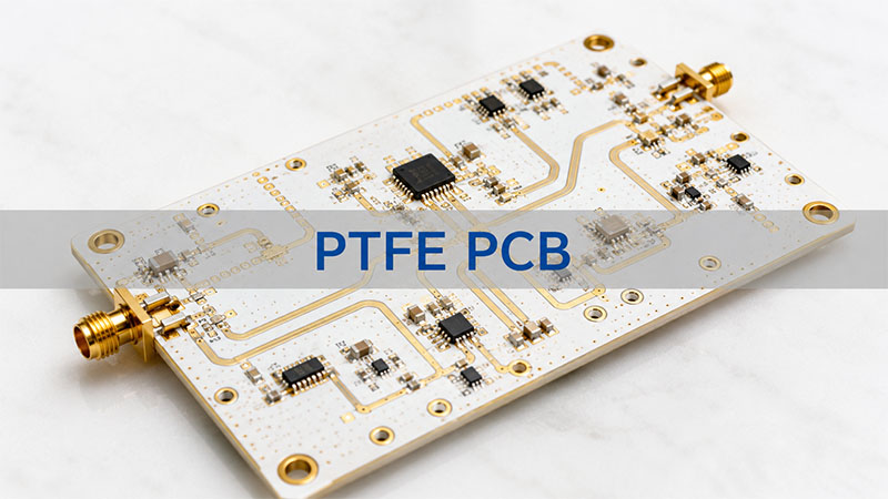
PTFE PCB projects usually come with clear business goals: stable RF performance, reliable fabrication, smooth assembly, and fewer delays before production. For buyers, the key question is not only “What is PTFE?” It is also “Can this manufacturer support my material, stack-up, impedance, RF connector assembly, and delivery needs?”
This guide helps you compare PTFE PCB materials, manufacturing capabilities, application fit, DFM support, and supplier selection factors.
What Is a PTFE PCB and Is It Right for Your Project?
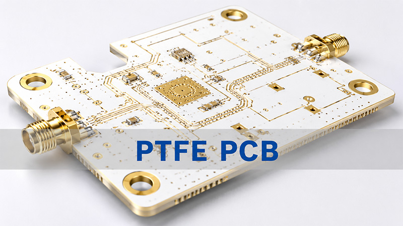
A PTFE PCB is a printed circuit board made with PTFE-based dielectric material. Engineers often choose it for RF, microwave, antenna, radar, and high-frequency communication products.
| Item | What It Means for Your Project |
|---|---|
| Material Type | PTFE-based high-frequency laminate |
| Main Purpose | Lower signal loss and stable RF behavior |
| Common Board Types | Single-sided, double-sided, multilayer, hybrid stack-up |
| Typical Circuits | RF lines, antenna circuits, microwave paths, radar modules |
| Main Buyer Concern | Can the supplier control material, impedance, drilling, and assembly? |
When PTFE PCB Is a Good Fit
| Your Project Need | Why PTFE Helps |
|---|---|
| RF signal transmission | Supports lower dielectric loss |
| Microwave circuit design | Helps keep signal behavior stable |
| Antenna board development | Supports controlled impedance and phase stability |
| Radar or communication module | Works well in high-frequency environments |
| Low-loss signal path | Reduces signal attenuation compared with standard FR4 |
When FR4 May Still Be Enough
| Project Condition | Better Choice |
|---|---|
| Low-frequency control board | FR4 |
| Cost-sensitive general electronics | FR4 |
| Simple power or LED board | FR4 or MCPCB |
| RF, microwave, radar, or antenna product | PTFE or other high-frequency laminate |
Quick takeaway:
Choose PTFE when signal quality matters more than material cost.
What PTFE PCB Materials and Laminates Can You Choose?
Material choice affects loss, impedance, lead time, cost, and long-term reliability. Buyers should not choose a laminate only by brand name. The material should match the frequency, stack-up, copper weight, and production plan.
| Material / Laminate Type | Common Use | Buyer Benefit |
|---|---|---|
| PTFE Laminate | RF and microwave boards | Low loss and stable electrical behavior |
| Rogers PTFE-Based Materials | Antenna, radar, telecom, aerospace electronics | Strong RF performance and trusted material data |
| Taconic Materials | RF modules, microwave circuits, antennas | Good high-frequency options for different budgets |
| Arlon Materials | RF, military, aerospace, and communication boards | Good fit for demanding high-frequency circuits |
| Nelco Materials | High-speed and RF-related boards | Useful for signal integrity and stable fabrication |
| Hybrid PTFE + FR4 Stack-Up | Mixed RF and control circuits | Balances cost, strength, and RF performance |
Key Material Properties to Check
| Property | Why Buyers Should Care |
|---|---|
| Dielectric Constant | Affects impedance and signal speed |
| Dissipation Factor | Affects signal loss |
| Laminate Thickness | Impacts controlled impedance |
| Copper Roughness | Influences high-frequency conductor loss |
| Thermal Stability | Supports reliable soldering and use |
| Moisture Absorption | Helps keep RF performance stable |
| Dimensional Stability | Supports drilling, routing, and layer alignment |
Practical Material Selection Guide
| If Your Product Is… | Consider This Material Direction |
|---|---|
| Antenna PCB | Low-loss PTFE or Rogers-based laminate |
| RF module | PTFE laminate with controlled impedance |
| Microwave board | Low dissipation factor laminate |
| Radar board | Stable dielectric and tight thickness tolerance |
| Mixed RF + digital board | Hybrid stack-up may reduce cost |
| Prototype stage | Choose available materials to shorten lead time |
Buyer note:
The best material is not always the most expensive one. The best material is the one that matches your RF target, budget, and delivery plan.
PTFE PCB Manufacturing Capabilities at EBest Circuit (Best Technology)
PTFE materials need tighter process control than standard FR4. Drilling, plating, lamination, impedance control, and assembly must work together.
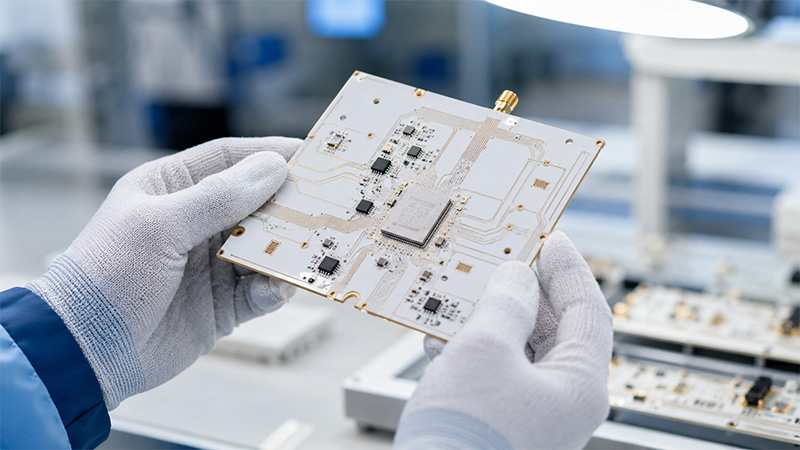
EBest Circuit (Best Technology) supports PTFE PCB fabrication, DFM review, PCBA assembly, component sourcing, testing, and turnkey electronics manufacturing.
| Capability | Technical Specification | Business Benefit |
|---|---|---|
| Material Coverage | PTFE, Rogers, Taconic, Arlon, Nelco, and other RF laminates | More choices for RF, microwave, antenna, and radar boards |
| Manufacturing Precision | 1–50 layers, 0.4–6.0 mm board thickness, 0.10 mm laser drilling, controlled impedance support | Better signal stability and lower production risk |
| Quality Certifications | ISO9001, ISO13485, IATF16949, AS9100D quality system support | Suitable for industrial and regulated projects |
| Turnaround Time | Prototype, small-batch, and volume production support | Faster validation and smoother production planning |
| Global Sourcing & Delivery | PCB fabrication, component sourcing, PCBA assembly, testing, and delivery | Less supplier coordination and easier project management |
What Customers Can Send for Review
| File / Information | Why It Helps |
|---|---|
| Gerber files | Checks circuit pattern and fabrication details |
| Drill files | Confirms hole size, via design, and plating needs |
| Stack-up | Confirms layer structure and impedance feasibility |
| Material request | Checks laminate availability and alternatives |
| Impedance requirement | Supports controlled RF performance |
| BOM | Helps with component sourcing and assembly |
| Pick-and-Place file | Supports SMT assembly preparation |
| Drawing or special notes | Clarifies tolerance, marking, finish, and testing needs |
Manufacturing Items Worth Confirming Early
- Laminate brand and grade
- Board thickness and tolerance
- Copper weight
- Controlled impedance target
- Minimum trace width and spacing
- Minimum hole size
- Via structure
- Surface finish
- RF connector type
- Testing requirement
Short takeaway:
Good PTFE PCB manufacturing starts before production. Early review helps avoid cost, schedule, and performance issues.
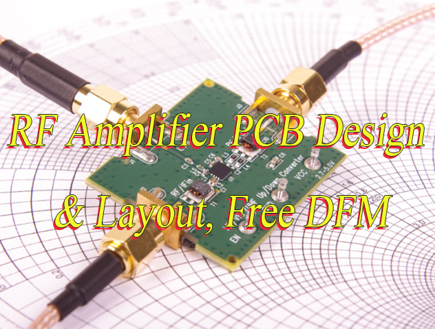
PTFE PCB Solutions for RF, Microwave, Antenna, and Communication Applications
PTFE-based boards serve projects where signal loss, impedance, and frequency stability matter. Buyers often search for a supplier because the product has moved beyond simple FR4 capability.
| Application | Common Requirement | How PTFE PCB Helps |
|---|---|---|
| RF Modules | Low-loss signal path | Supports stable RF transmission |
| Microwave Circuits | Controlled signal behavior | Helps reduce dielectric loss |
| Antenna Boards | Stable impedance and phase | Supports consistent radiation performance |
| Radar Systems | High-frequency accuracy | Helps with signal stability |
| Satellite Communication | Reliable RF path | Supports low-loss designs |
| Wireless Infrastructure | Stable high-frequency operation | Fits RF front-end and antenna systems |
| Test Equipment | Repeatable signal performance | Supports accurate measurement circuits |
| Industrial Communication | Reliable signal transfer | Helps in harsh or demanding environments |
Application-Based Buying Checklist
| Question | Why It Matters |
|---|---|
| What is the operating frequency? | Helps select the right laminate |
| What impedance do you need? | Guides stack-up and trace width |
| Does the board need assembly? | Affects footprint, finish, and PCBA plan |
| Will the board use RF connectors? | Requires connector launch review |
| Is the product for prototype or volume? | Affects material choice and lead time |
| Does the product need special testing? | Impacts cost and delivery schedule |
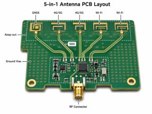
Common RF Board Features
- 50-ohm transmission lines
- Microstrip or stripline structure
- Ground via stitching
- RF connector launch area
- Shielding area
- Tight trace control
- Low-loss laminate
- Stable reference plane
Project note:
For RF and microwave boards, the PCB is not only a carrier. It becomes part of the signal path.
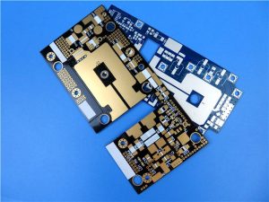
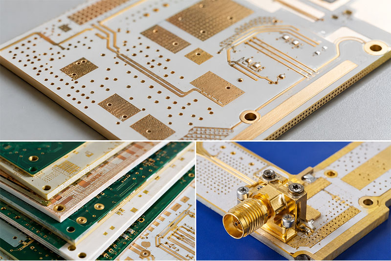
PTFE Multilayer PCB Solutions for Complex High-Frequency Projects
Complex RF products often need more than a simple double-sided board. A multilayer PTFE structure can combine RF signal layers, ground planes, power layers, and control circuits.
| Multilayer Need | What It Supports |
|---|---|
| RF Signal Layer | Controlled high-frequency routing |
| Ground Plane | Better return path and shielding |
| Power Layer | Stable power distribution |
| Digital Control Layer | Supports mixed RF and control functions |
| Via Stitching | Improves grounding around RF areas |
| Hybrid Stack-Up | Balances cost, RF performance, and strength |
Commercial Benefits of PTFE Multilayer Support
| Buyer Concern | Multilayer Solution |
|---|---|
| Board size is too large | More routing layers reduce area |
| RF and digital circuits need separation | Layer planning improves isolation |
| Signal path needs stable reference | Ground planes support impedance |
| Product needs compact design | Multilayer structure supports integration |
| Cost must stay controlled | Hybrid stack-up can help |
Manufacturing Risks to Review
| Risk Area | What the Manufacturer Should Check |
|---|---|
| Layer alignment | Registration between RF and ground layers |
| Lamination | Bonding material and pressure control |
| Drilling | Hole quality in PTFE material |
| Plating | Reliable copper in vias and holes |
| Impedance | Trace width, dielectric height, and copper thickness |
| Hybrid structure | CTE difference between PTFE and FR4 |
Best-Fit Projects
- RF modules with dense routing
- Antenna control boards
- Radar electronics
- Microwave communication boards
- Mixed RF and digital products
- Compact high-frequency assemblies
Buyer note:
A multilayer PTFE PCB needs strong front-end engineering review. It should not move directly from file upload to production without stack-up confirmation.
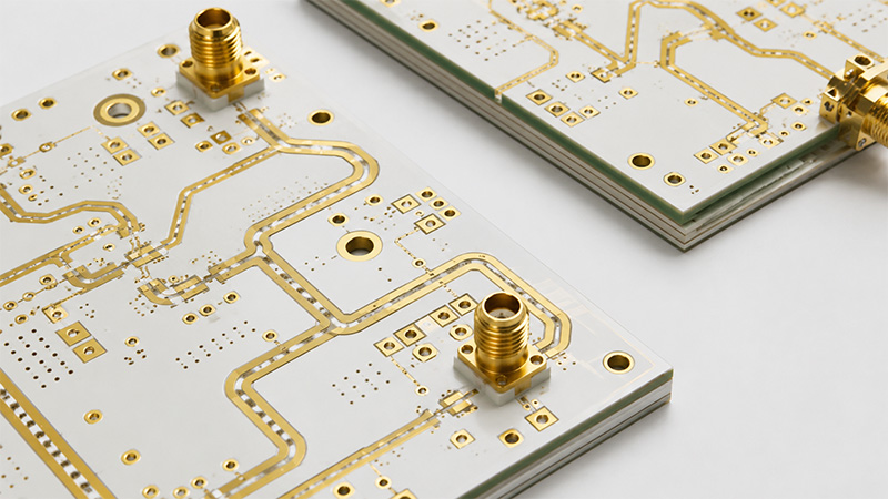
RF Connector Assembly Support for PTFE PCB Projects
RF connectors affect both assembly quality and signal performance. For many high-frequency boards, the connector launch area decides how smoothly the signal enters or leaves the PCB.
| RF Connector Item | What to Check | Why It Matters |
|---|---|---|
| Connector Type | SMA, SMB, MMCX, U.FL, coaxial connector | Matches frequency, size, and cable interface |
| Footprint | Pad size, hole size, ground pad, solder mask opening | Supports accurate assembly |
| Impedance Transition | Connector pin to RF trace | Reduces signal reflection |
| Ground Via Stitching | Vias near connector ground pads | Improves return path |
| Mechanical Support | Mounting holes, solder area, board edge | Improves connector strength |
| Soldering Control | Temperature, alignment, solder volume | Supports stable electrical and mechanical quality |
| Inspection | Visual check, X-ray, continuity, RF test if required | Confirms final assembly quality |
RF Connector Launch Checklist
| Design / Assembly Point | Recommended Review |
|---|---|
| Center pin pad | Match connector datasheet |
| Ground pads | Provide enough solder area |
| Via placement | Keep return path short |
| Trace transition | Avoid sudden width changes |
| Board edge | Confirm outline and connector position |
| Surface finish | Choose finish suitable for soldering |
| Panel design | Support stable assembly handling |
Business Value of Connector Assembly Support
- Reduces mismatch between PCB design and assembly
- Helps avoid weak solder joints
- Improves RF signal transition
- Supports one-stop PCB + PCBA supply
- Reduces communication across suppliers
- Makes prototype validation faster
Short takeaway:
RF connector assembly is not a small detail. It directly affects signal quality, board strength, and customer testing results.
DFM Review Support Before PTFE PCB Production
DFM review helps customers find production risks before fabrication starts. For PTFE PCB projects, this step is especially useful because high-frequency boards often have tight material and impedance requirements.
| DFM Review Item | What EBest Circuit Checks | Customer Benefit |
|---|---|---|
| Material Match | Laminate type, thickness, copper weight | Avoids wrong material selection |
| Stack-Up | Layer order, dielectric height, bonding material | Supports impedance and reliability |
| Trace Width / Spacing | Manufacturability and RF routing limits | Reduces production risk |
| Impedance Target | 50-ohm or custom impedance requirements | Improves RF consistency |
| Via Design | Hole size, annular ring, via placement | Supports plating reliability |
| Copper Balance | Copper distribution across layers | Helps board flatness |
| Surface Finish | ENIG or other finish options | Supports soldering and contact quality |
| RF Connector Area | Footprint, launch, grounding, mechanical support | Improves assembly and signal transition |
| Panelization | Panel size, breakaway, handling | Supports smoother production |
Typical Problems DFM Can Catch
| Problem | Possible Impact |
|---|---|
| Trace width does not match impedance model | RF performance may shift |
| Via too close to RF trace | Signal path may suffer |
| Connector pad does not match datasheet | Assembly issue or weak solder joint |
| Copper area is uneven | Board flatness risk |
| Stack-up lacks clear reference plane | Poor signal return path |
| Material is hard to source | Longer lead time |
Files Needed for DFM Review
- Gerber files
- Drill files
- Stack-up drawing
- Impedance table
- Material preference
- BOM, if assembly is required
- Connector datasheet
- Special tolerance notes
Buyer note:
DFM review does not replace circuit design. It helps turn your design into a board that the factory can build with better control.
Why Choose EBest Circuit (Best Technology) for PTFE PCB Manufacturing?
Choosing a PTFE PCB supplier should not depend only on price. High-frequency boards need material knowledge, process control, engineering support, and assembly experience.
| Customer Need | EBest Circuit Support |
|---|---|
| High-frequency PCB fabrication | Supports PTFE and RF laminate projects |
| Material selection help | Reviews Rogers, Taconic, Arlon, Nelco, and other options |
| Stack-up review | Checks layer structure and impedance feasibility |
| Controlled impedance | Supports RF and high-speed requirements |
| DFM before production | Helps reduce manufacturing risks |
| RF connector assembly | Supports footprint, grounding, soldering, and inspection review |
| PCBA assembly | Supports SMT, through-hole, sourcing, and testing |
| Project stages | Supports prototype, small batch, and volume production |
| Global delivery | Supports overseas customers with one-stop service |
Why This Matters for Buyers
| Buying Concern | How One-Stop Support Helps |
|---|---|
| Too many suppliers | PCB, sourcing, assembly, and testing can stay together |
| RF board has tight requirements | Engineering review starts before production |
| Material choice is unclear | Team can suggest workable options |
| Assembly needs RF connectors | PCB and PCBA teams can align early |
| Prototype schedule is tight | Early review helps reduce redesign delays |
| Project may move to batch production | Process records support repeat orders |
Good Projects to Discuss with EBest Circuit
- RF PCB fabrication
- PTFE PCB prototype
- Rogers-based high-frequency board
- Antenna PCB
- Microwave PCB
- Multilayer RF PCB
- RF connector assembly
- Turnkey PCBA for high-frequency products
Request a Quote
To get a faster and more accurate quotation, send:
| Required Information | Helpful Details |
|---|---|
| Gerber files | Required for PCB quotation |
| Stack-up | Needed for impedance and layer review |
| Material request | Rogers, PTFE, Taconic, Arlon, Nelco, or equivalent |
| Quantity | Prototype, small batch, or volume |
| Surface finish | ENIG, immersion silver, or other options |
| BOM | Required for PCBA quotation |
| Pick-and-Place file | Required for SMT assembly |
| Testing requirement | Electrical test, AOI, X-ray, functional test, RF test if needed |
For PTFE PCB fabrication or turnkey assembly support, contact: sales@bestpcbs.com
FAQs About PTFE PCB Manufacturing
| Question | Answer |
|---|---|
| Is PTFE PCB better than FR4? | PTFE performs better in RF, microwave, and low-loss applications. FR4 still works well for many standard electronics. |
| What applications need PTFE PCB? | RF modules, antenna boards, microwave circuits, radar electronics, satellite communication, and wireless equipment often need it. |
| Can PTFE PCB support multilayer designs? | Yes. It can support multilayer and hybrid stack-ups when the manufacturer controls lamination, drilling, plating, and impedance. |
| Can EBest Circuit support PTFE PCB assembly? | Yes. EBest Circuit supports PCB fabrication, component sourcing, SMT assembly, through-hole assembly, testing, and delivery. |
| What files should I send for a quote? | Send Gerber files, drill files, stack-up, material request, impedance requirement, quantity, and drawings. For assembly, send BOM and Pick-and-Place files. |
| Can PTFE PCB use RF connectors? | Yes. RF connectors such as SMA, SMB, MMCX, U.FL, and coaxial types can be assembled when the footprint and grounding design match the connector requirement. |
| Why does PTFE PCB cost more than FR4? | PTFE laminate costs more. The manufacturing process also needs tighter drilling, plating, lamination, and impedance control. |
| Can I use Rogers material for PTFE PCB? | Yes. Rogers offers high-frequency materials for RF and microwave products. The right choice depends on frequency, loss target, stack-up, and budget. |
| Does DFM review help before production? | Yes. It can catch stack-up, impedance, via, connector, copper balance, and manufacturability issues before fabrication. |
| Can PTFE PCB support prototype and batch production? | Yes. A capable manufacturer can support samples first, then help move the project to small-batch or volume production. |
Final Takeaway
| If You Need… | Focus On… |
|---|---|
| Stable RF signal | PTFE laminate, impedance, copper control |
| Reliable production | DFM review, drilling, plating, lamination |
| Compact RF design | Multilayer or hybrid stack-up |
| Complete assembly | RF connector support, SMT, testing |
| Fewer supplier issues | One-stop PCB + PCBA service |
| Faster quotation | Complete Gerber, stack-up, BOM, and requirement files |
PTFE PCB manufacturing is a project-level decision, not just a material choice. Buyers should check the laminate, stack-up, impedance, RF connector design, DFM support, assembly plan, and supplier capability before production.
EBest Circuit (Best Technology) helps customers move from RF board design files to reliable PCB fabrication and PCBA assembly with practical engineering support.