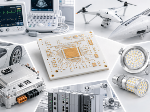
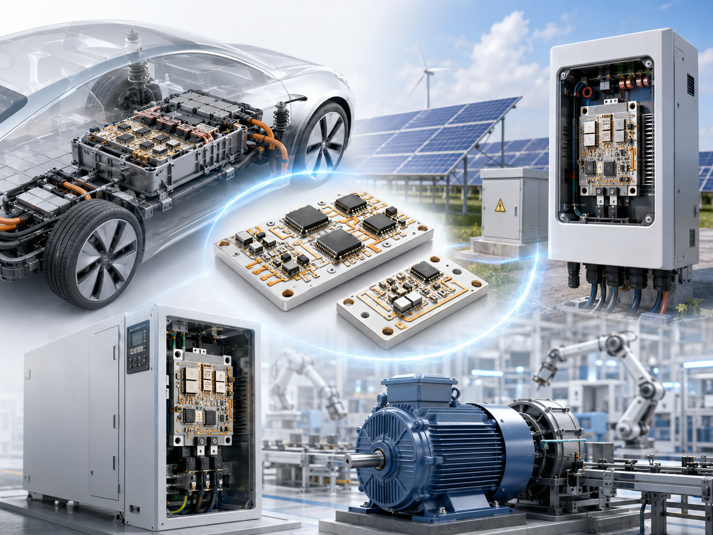
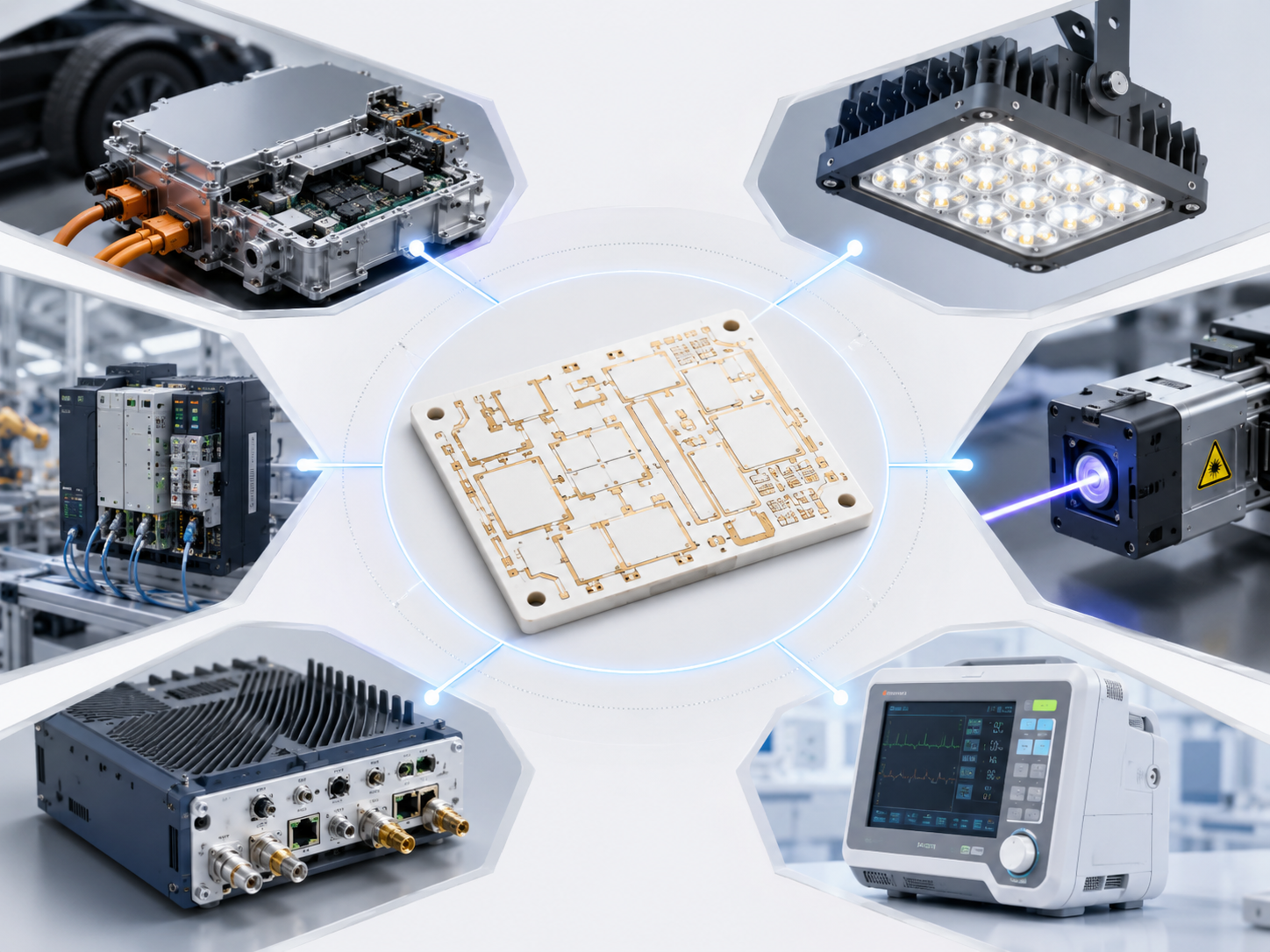
Ceramic PCB for automotive electronics is becoming an important choice in EV inverters, LED headlights, onboard chargers, DC-DC converters, sensors, and battery systems. In these applications, the circuit board often does more than connect components. It also helps transfer heat, provide insulation, and support long-term reliability in compact automotive modules.
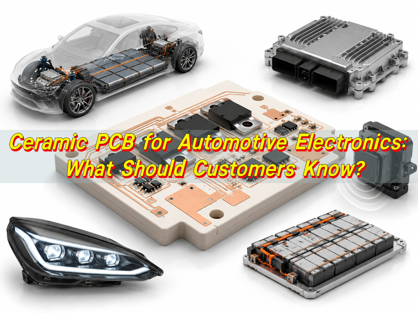
A ceramic PCB for automotive electronics is used when FR4 cannot provide enough thermal performance, voltage insulation, or stability in a compact structure. It is not the right choice for every automotive board. For many control circuits, FR4 remains practical and cost-effective. Ceramic PCB becomes valuable when the board is close to heat sources, power devices, high-current paths, or high-voltage sections.
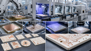
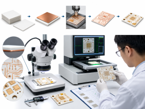
EBest Circuit supports ceramic PCB manufacturing, ceramic PCB prototypes, and PCB assembly for automotive and EV applications. For customers, the best starting point is simple: define the heat, voltage, current, space, and reliability requirements before choosing the substrate.
What Is a Ceramic PCB for Automotive Electronics?
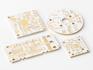
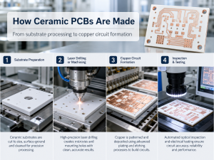
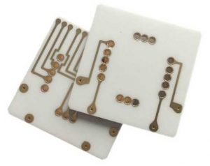
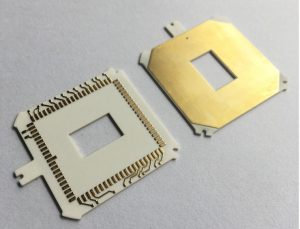
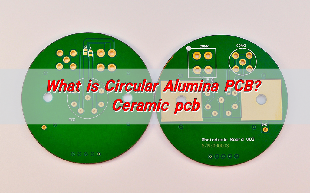
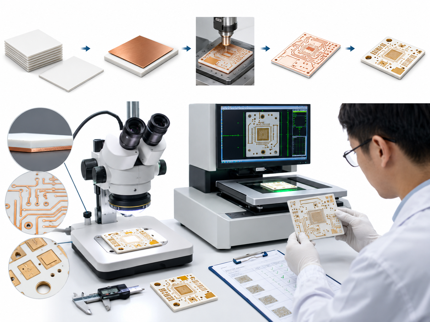
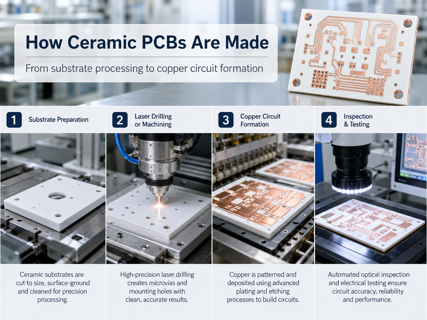
A ceramic PCB for automotive electronics is a circuit board or substrate that uses ceramic material as the base instead of FR4 laminate. Common ceramic materials include alumina, aluminum nitride, and silicon nitride. Copper circuits are formed on the ceramic surface through DPC, DBC, AMB, thick film, thin film, or other metallization processes.
The main purpose of using ceramic is to combine electrical insulation with heat transfer. This is useful in automotive systems where heat must move from power devices to a heat sink, metal housing, or cooling plate while the circuit remains electrically isolated.
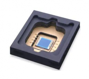
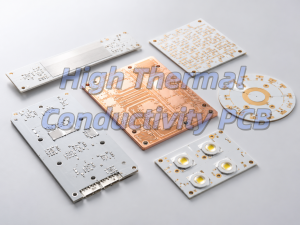
Ceramic PCB boards are commonly used in EV power modules, automotive LED lighting, onboard chargers, DC-DC converters, high-temperature sensors, heater circuits, and powertrain modules. A small alumina sensor substrate and a thick copper AMB substrate for an EV drive system are both ceramic-based products, but their structures and costs are very different.
For customers requesting a ceramic PCB prototype, the process type matters. DPC is often used for fine circuit patterns. DBC and AMB are better suited for thick copper, high current, and power module applications. Thick film ceramic circuits are used when printed resistors, heater traces, or functional paste layers are required.
Why Are Ceramic PCBs Used in Automotive Electronics?
Ceramic PCBs are used when the board must handle heat, voltage, or harsh working conditions better than standard FR4. In automotive electronics, this usually happens near power semiconductors, LEDs, balancing resistors, current sensors, heating elements, and high-voltage power sections.
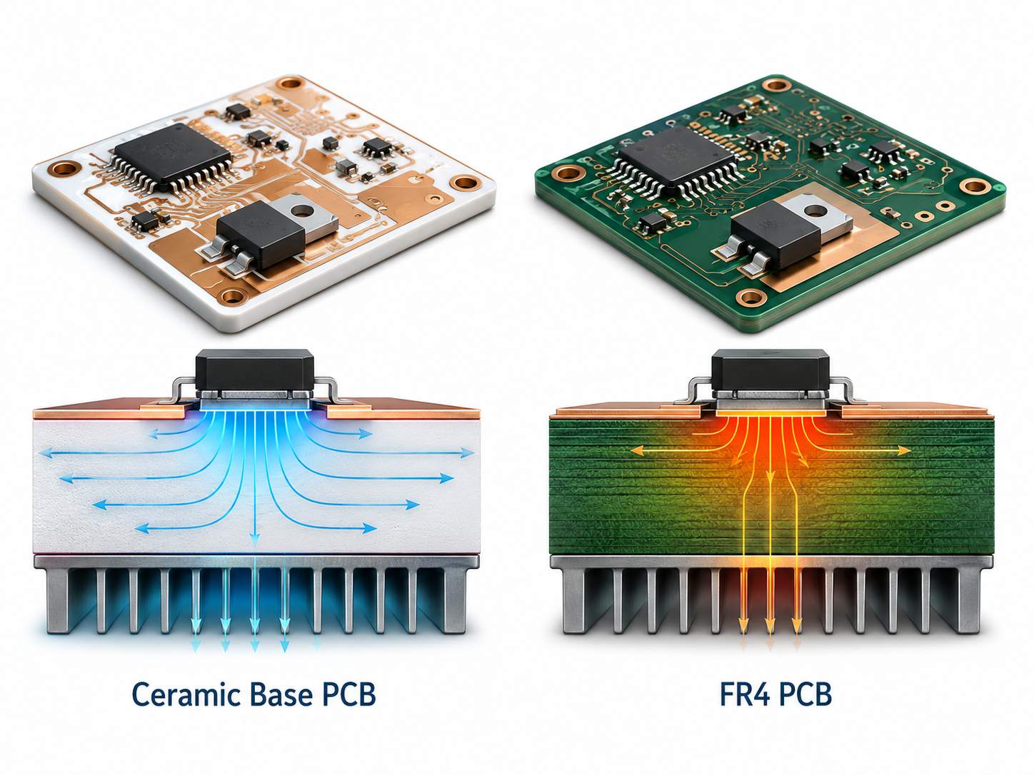
The biggest advantage is thermal performance. FR4 is a poor heat conductor. Ceramic materials can transfer heat more efficiently while still providing insulation. This makes them useful in modules where the substrate sits between a hot component and a cooling structure.
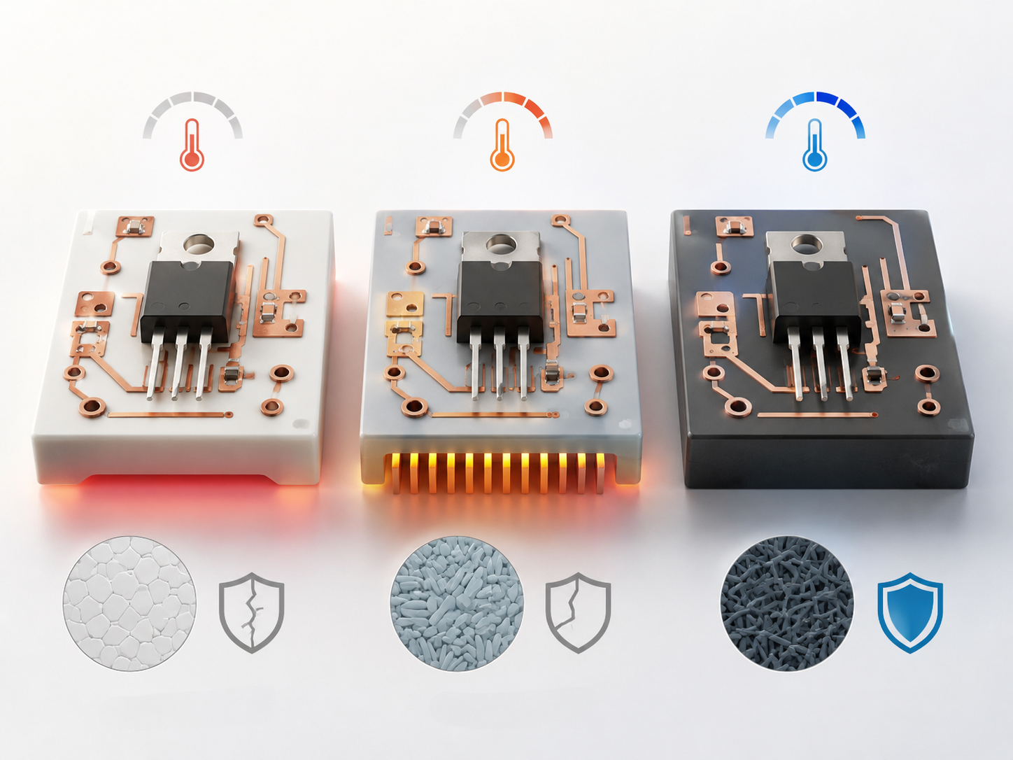
Ceramic PCBs are also stable under temperature changes. Vehicle electronics go through repeated heating and cooling during driving, charging, parking, and load changes. A stable ceramic substrate helps reduce stress on solder joints, copper layers, chips, and bonded interfaces.
Ceramic PCB is usually worth considering when the design has:
- High heat in a small area
- High-voltage insulation requirements
- Power devices mounted close to the substrate
- Limited space for heat sinks or airflow
- Repeated thermal cycling
- Thick copper or high-current paths
- A need for long-term stability in a harsh environment
If the board mainly carries signals or low-power control circuits, FR4 is usually enough. Ceramic should be used where it solves a clear engineering problem.
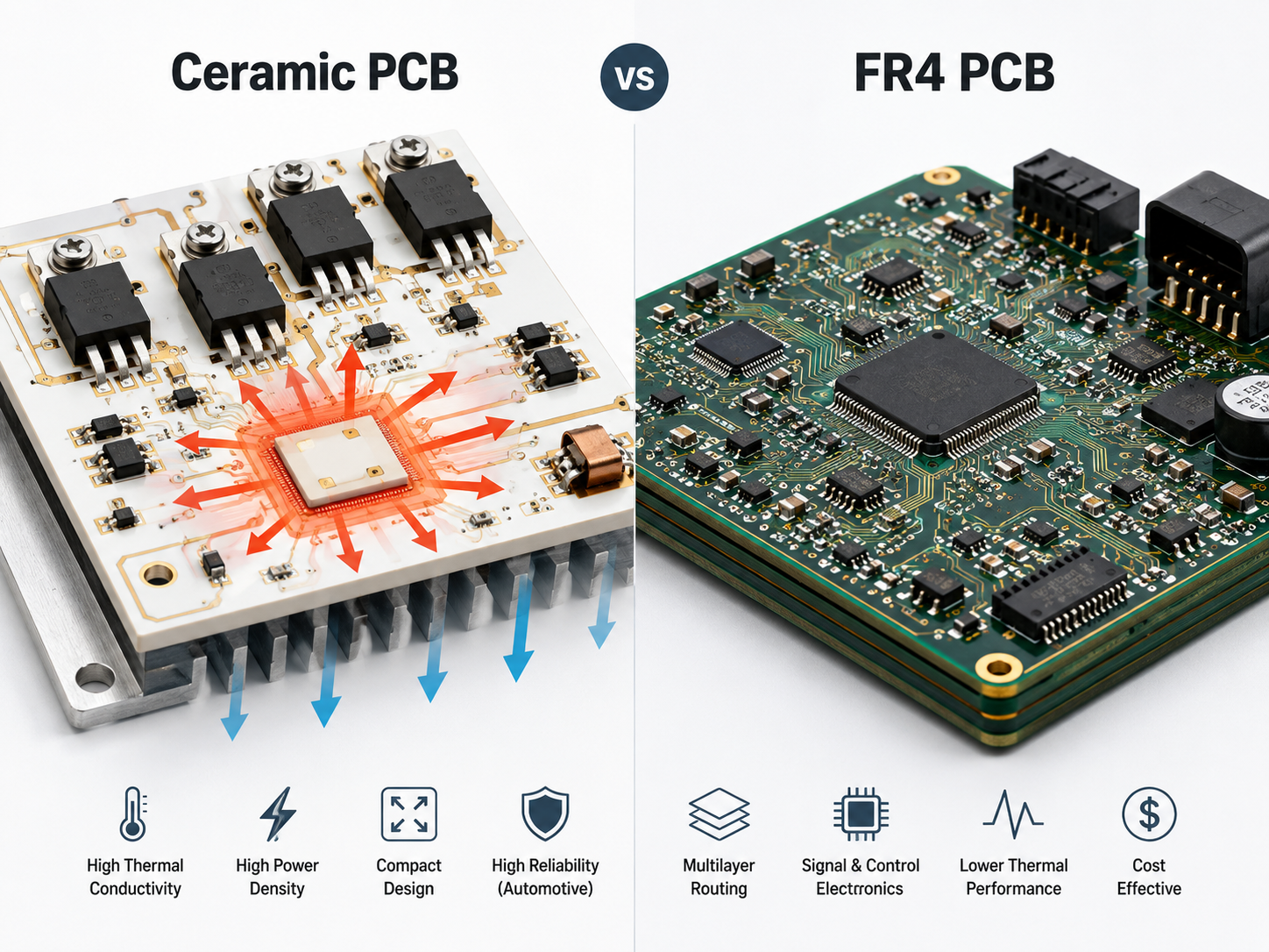
How Is a Ceramic PCB Board Different from an FR4 PCB?
Ceramic PCB and FR4 PCB are used for different design priorities. FR4 is strong in routing flexibility, multilayer design, cost control, and general electronics. Ceramic PCB is stronger in heat transfer, insulation, dimensional stability, and power-density applications.
| Item | Ceramic PCB Board | FR4 PCB |
|---|---|---|
| Base material | Alumina, AlN, Si3N4, or other ceramic | Glass fiber and epoxy resin |
| Main value | Thermal transfer and insulation | Routing flexibility and cost control |
| Thermal conductivity | Much higher, depending on ceramic type | Low, commonly around 0.25–0.35 W/m·K |
| Heat resistance | Strong in high-temperature areas | Limited by resin system and Tg grade |
| Electrical insulation | Excellent for power and high-voltage use | Good for standard circuits |
| Copper structure | Can support thick copper in DBC or AMB | Better for standard multilayer PCB routing |
| Typical use | EV power modules, LEDs, sensors, power converters | ECU, BMS control board, infotainment, body electronics |
| Cost | Higher | Lower |
FR4 is the better first choice for control boards, communication boards, and cost-sensitive electronics. Ceramic PCB is the better option when the board must act as a thermal path or an insulating power substrate.
When Should You Choose Ceramic Substrate vs FR4 in Automotive Electronics?
Choose ceramic substrate when heat, voltage, or current density is the design limit. Choose FR4 when the board mainly needs signal routing, control, and standard assembly.
In many automotive products, both materials can be used in the same system. For example, an EV charger may use FR4 for the control board and ceramic substrate for the power section. A BMS may use FR4 for monitoring and communication, while using ceramic near balancing resistors or heat-generating parts.
| Design Condition | Better Choice | Reason |
| Low-power control circuit | FR4 PCB | Lower cost and easier multilayer routing |
| Infotainment or communication board | FR4 PCB | Better for dense signal routing |
| High-power LED module | AlN ceramic PCB or metal core PCB | Better heat transfer |
| EV inverter power stage | DBC or AMB ceramic substrate | Handles heat, current, and insulation |
| BMS main control board | FR4 PCB | Mostly signal and monitoring circuits |
| BMS resistor hot zone | Ceramic PCB or metal core PCB | Helps spread local heat |
| High-temperature sensor | Alumina or AlN ceramic PCB | Stable near heat sources |
| Compact DC-DC converter | Ceramic PCB | Reduces thermal resistance |
Before choosing ceramic, customers should provide power loss, current load, operating voltage, target temperature, board size, copper thickness, cooling method, and assembly requirements. Without these details, material selection is incomplete.
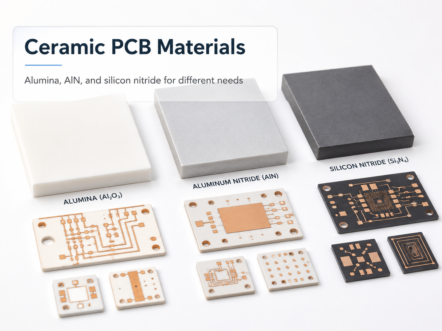
What Ceramic PCB Materials Are Used in Automotive Applications?
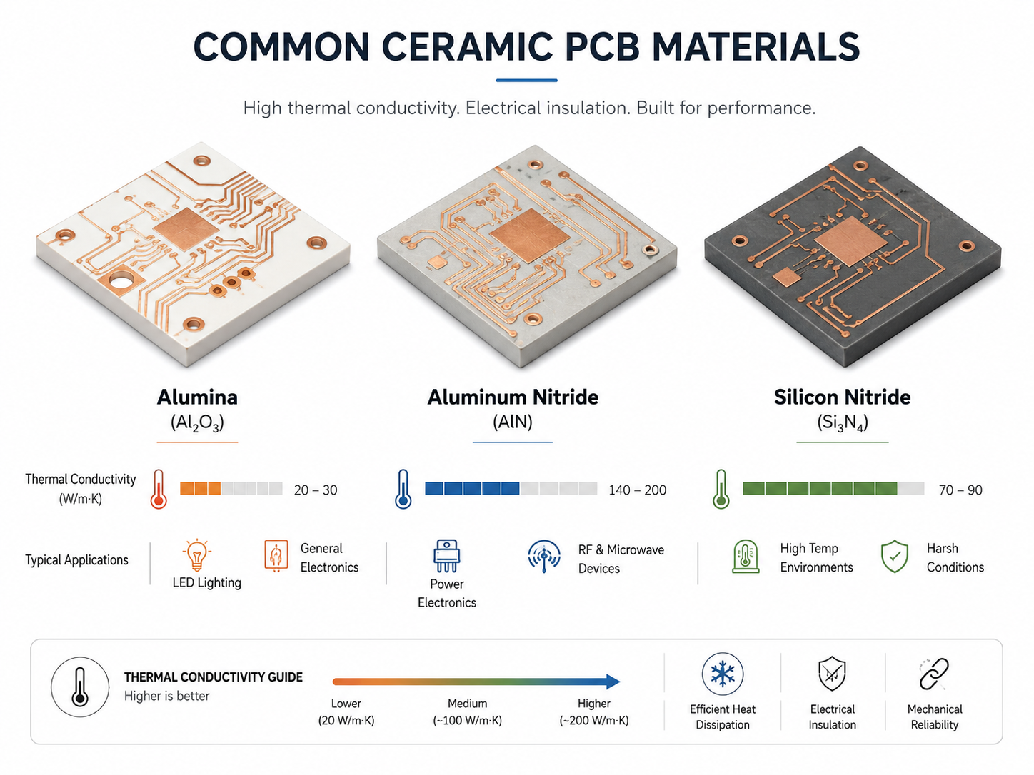
The main ceramic PCB materials for automotive applications are alumina, aluminum nitride, and silicon nitride. Each material fits a different use case.
Alumina is the most common option. It is stable, insulating, mature in production, and more economical than AlN or Si3N4. It is often used for sensors, thick film circuits, heater circuits, and moderate-power modules.
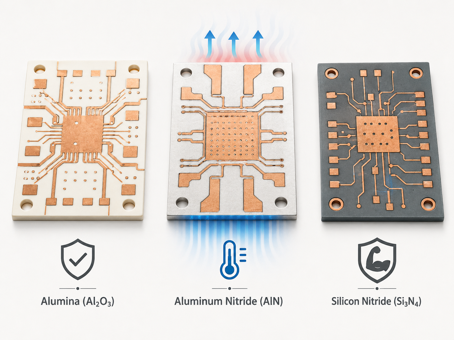
Aluminum nitride is selected when heat transfer is the main requirement. It has much higher thermal conductivity than alumina and is widely used in automotive LED lighting, compact power modules, and high-heat areas.
Silicon nitride is selected for mechanical reliability and thermal cycling performance. It is often used in AMB substrates for EV inverter and drive system modules.
| Material or Structure | Main Feature | Automotive Use |
| Alumina ceramic | Stable, insulating, cost-effective | Sensors, heater circuits, thick film modules |
| AlN ceramic | High thermal conductivity | LED lighting, power modules, compact thermal designs |
| Si3N4 ceramic | Strong thermal cycling reliability | EV inverter and drive systems |
| DPC ceramic PCB | Fine circuits and plated copper | LEDs, sensors, precision circuits |
| DBC ceramic substrate | Thick copper bonded to ceramic | Power modules and high-current circuits |
| AMB ceramic substrate | Strong copper-to-ceramic bonding | EV drive systems and SiC power modules |
| Thick film ceramic | Printed conductor or resistor layers | Sensors and heater modules |
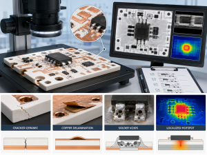
Material selection should not rely only on thermal conductivity. Copper thickness, ceramic thickness, bonding strength, insulation distance, surface finish, assembly process, and cost target should also be reviewed.
Why Is AlN Ceramic PCB Used for Automotive LED Lighting?
AlN ceramic PCB is used in automotive LED lighting because high-power LEDs generate concentrated heat. In headlights, daytime running lights, matrix LED systems, and EV lighting modules, the board must move heat away from the LED package quickly.
AlN provides a strong thermal path while keeping electrical insulation. This helps the lighting module maintain stable brightness, color consistency, and service life. It is especially useful in compact lamp designs where airflow is limited and the heat sink area is small.
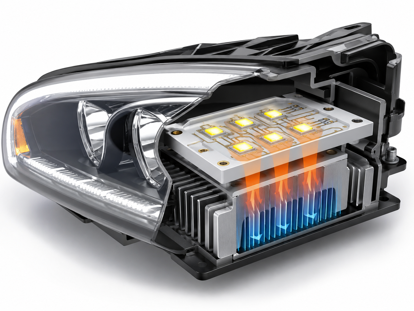
The thermal path usually follows this route: LED package, solder joint, copper layer, AlN ceramic substrate, thermal interface material, heat sink, and lamp housing. The ceramic board improves the substrate part of this path, but the full structure must also be well designed.
| Lighting Requirement | Why AlN Helps |
| High LED power density | Transfers heat away from small LED areas |
| Slim lamp structure | Supports compact thermal design |
| Matrix LED layout | Helps manage multiple heat sources |
| Stable brightness | Reduces excessive temperature rise |
| Color consistency | Keeps LED operation more stable |
| Electrical insulation | Isolates copper circuits from the housing |
For customers, LED power, copper thickness, soldering method, housing design, thermal interface material, and surface finish should be confirmed before making an AlN ceramic PCB prototype.
How Does Ceramic PCB Thermal Conductivity Help EV Systems?
Ceramic PCB thermal conductivity helps EV systems by reducing the thermal bottleneck between power components and the cooling structure. This is important in inverters, onboard chargers, DC-DC converters, power distribution units, LED drivers, and battery-related circuits.
| Material | Typical Thermal Conductivity Range | Meaning in EV Systems |
| FR4 | About 0.25–0.35 W/m·K | Suitable for control and signal boards |
| Alumina ceramic | About 20–30 W/m·K | Good for cost-balanced ceramic designs |
| AlN ceramic | About 140–180 W/m·K | Strong for compact high-power modules |
| Si3N4 ceramic | About 70–90 W/m·K | Good for thermal cycling reliability |
| Copper | About 400 W/m·K | Used for current and heat spreading |
Higher thermal conductivity helps move heat away from IGBTs, SiC MOSFETs, LEDs, power resistors, and other hot components. However, customers should not look at substrate thermal conductivity alone. Total thermal resistance is more important.
Ceramic thickness, copper thickness, solder layer, thermal interface material, heat sink contact, mounting pressure, and cooling method all affect final temperature. A high-performance ceramic substrate still needs a good mechanical and thermal design around it.
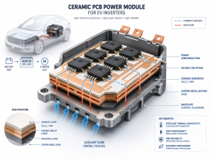
How Are Ceramic PCBs Used in EV Power Electronics?
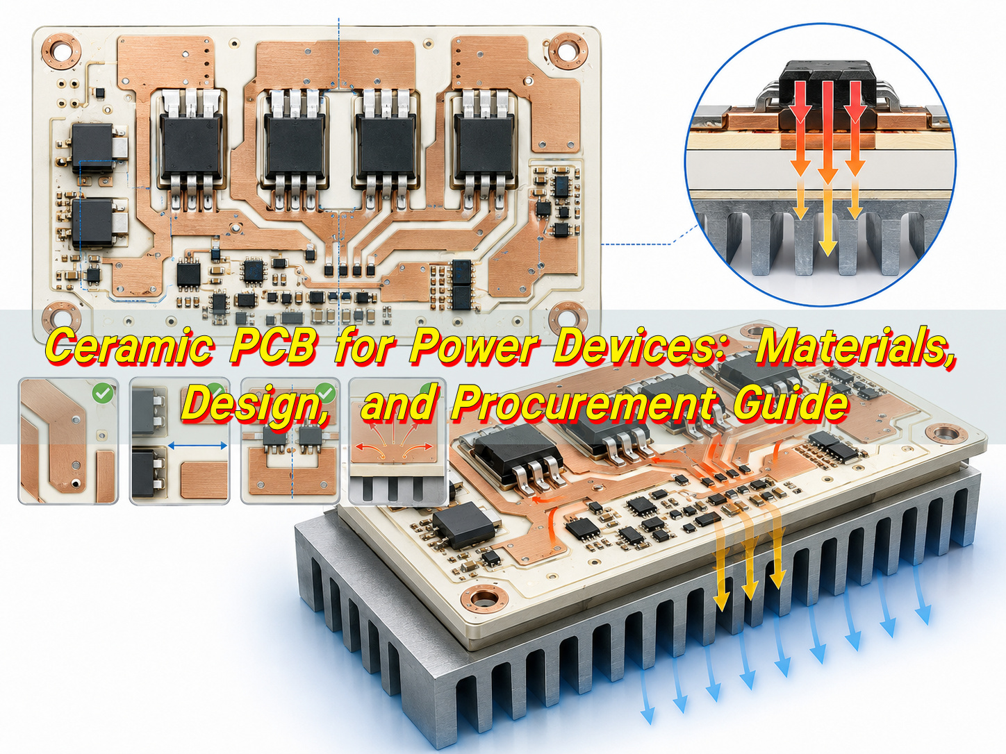
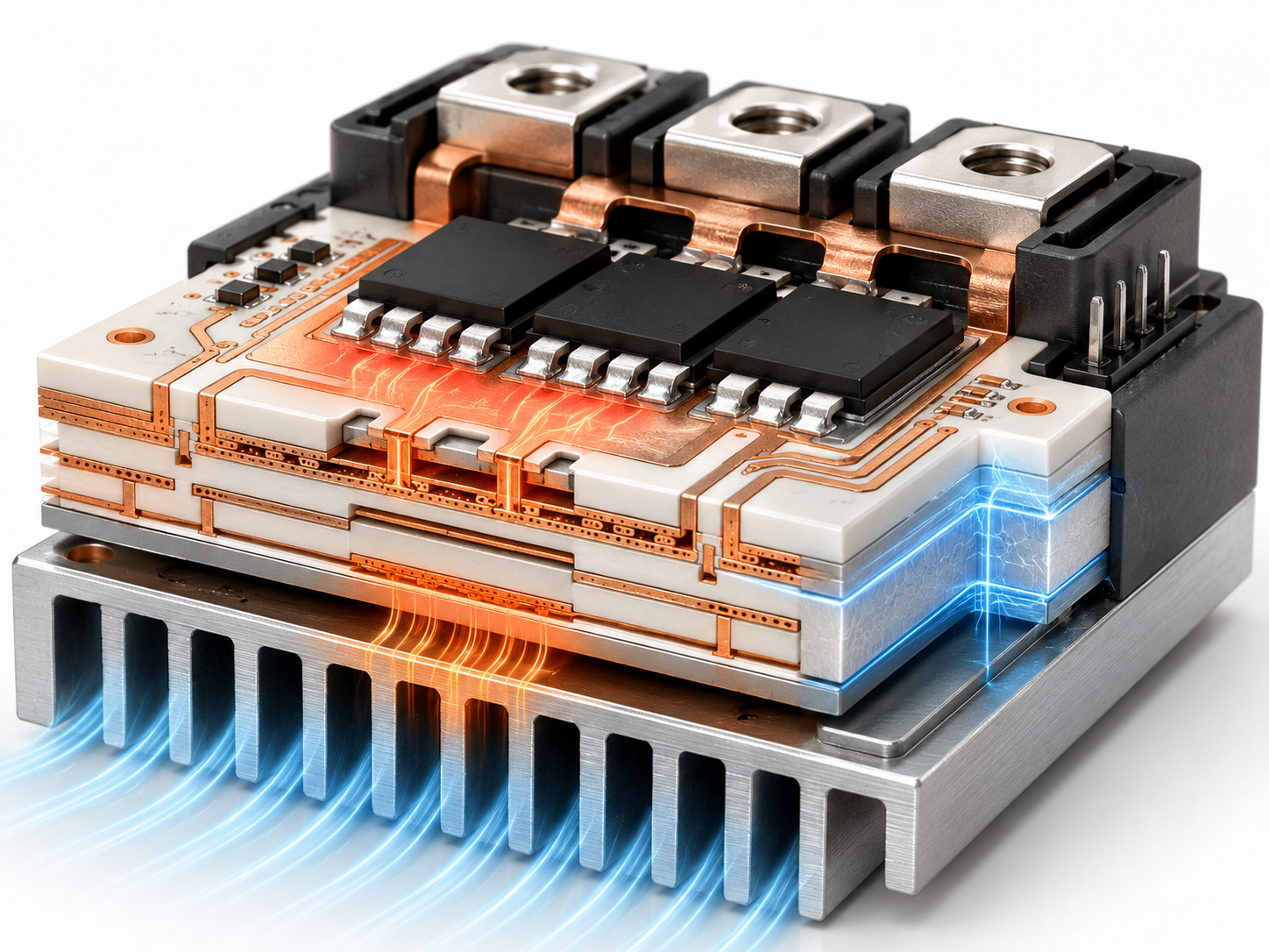
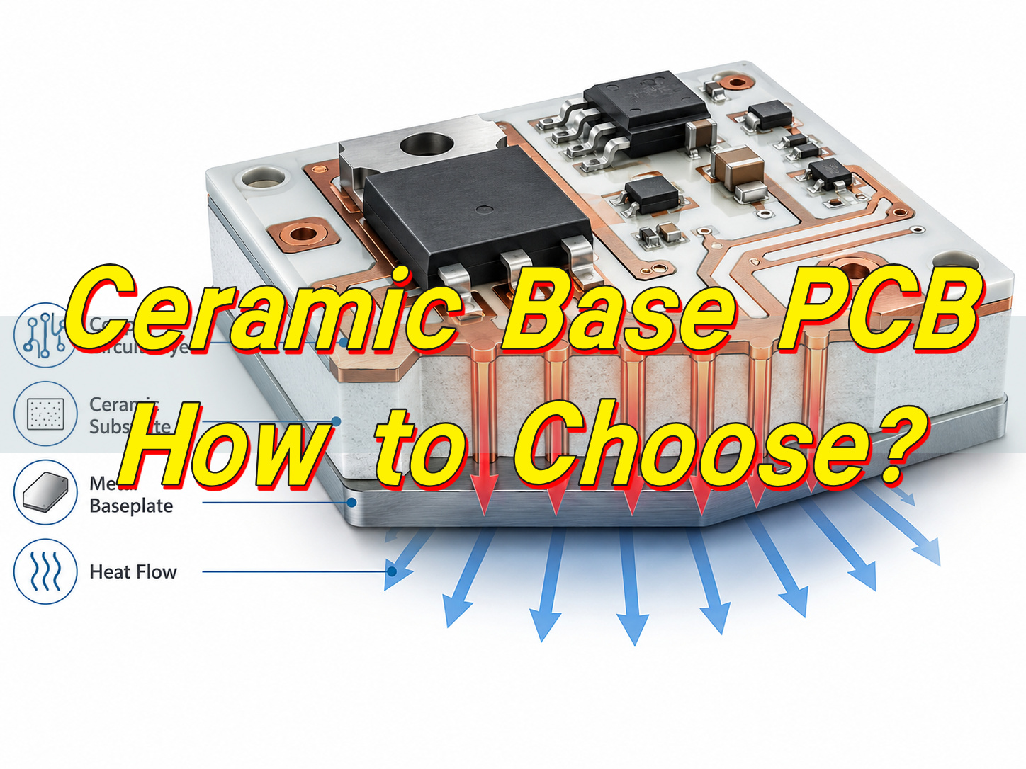
Ceramic PCBs are used in EV power electronics as insulating thermal substrates. They support power devices, carry current through copper, transfer heat to the cooler, and maintain electrical isolation.
In traction inverters, ceramic substrates are often used under IGBTs or SiC MOSFETs. Heat moves from the semiconductor into copper, through the ceramic, and toward the cooling plate. The ceramic layer keeps the high-voltage circuit isolated from the cooler.

In onboard chargers, ceramic boards can be used near switching devices, rectifiers, and other heat-generating power components. In DC-DC converters, ceramic substrates may be used in the power section, while FR4 remains suitable for the control section.
Typical applications include:
- Traction inverter power modules
- SiC MOSFET and IGBT substrates
- Onboard charger power sections
- DC-DC converter thermal modules
- Power distribution circuits
- Electric compressor drive electronics
- High-power LED driver modules
- Ceramic PCB assembly for powertrain modules
For EV power electronics, copper design is critical. Copper thickness affects current capacity and heat spreading. Copper shape affects stress. Isolation gaps affect voltage safety. Ceramic thickness affects thermal resistance and mechanical strength. These details should be checked before prototype production.
How Is AMB Ceramic PCB Used in Electric Vehicle Drive Systems?
AMB ceramic PCB is used in electric vehicle drive systems as a high-reliability power substrate. AMB means Active Metal Brazing. Copper is bonded to ceramic through an active brazing alloy, creating a strong copper-to-ceramic connection.
EV drive systems create repeated heating and cooling during acceleration, regenerative braking, and load changes. The substrate must handle current, heat, insulation, vibration, and thermal cycling. AMB is selected when bonding strength and long-term reliability are more important than lowest cost.
AMB substrates are commonly made with AlN or Si3N4. AlN AMB is used when high thermal conductivity is the priority. Si3N4 AMB is used when thermal cycling and mechanical reliability are more important.
| Substrate Type | Main Feature | Automotive Use |
| Alumina DBC | Mature and cost-effective | Standard power modules |
| AlN DBC | Better heat transfer | Higher power-density modules |
| AlN AMB | High thermal transfer and strong bonding | Compact power modules |
| Si3N4 AMB | Strong thermal cycling reliability | EV traction inverter modules |
AMB ceramic PCB is especially useful for SiC power modules. SiC devices can operate at high power density, so the substrate must support concentrated heat and strong copper adhesion. AMB gives the module a more robust base for demanding drive system conditions.
Can Ceramic PCBs Be Used for BMS in Electric Vehicles?
Ceramic PCBs can be used for BMS in electric vehicles, but usually only in selected areas. Most BMS main boards use FR4 because they handle voltage monitoring, communication, control, and low-power signal processing.
Ceramic becomes useful where heat or insulation stress is higher. The most common example is the balancing resistor area. During cell balancing, resistors can generate local heat. A ceramic substrate can help spread that heat and protect nearby components.
Ceramic PCB may also be considered for current sensing areas, temperature sensing modules, compact protection circuits, or battery modules exposed to elevated temperature.
| BMS Area | Suitable PCB Choice | Reason |
| Main control board | FR4 PCB | Good for signal routing and cost control |
| Communication circuit | FR4 PCB | Low power and standard assembly |
| Voltage monitoring board | FR4 or ceramic PCB | Depends on location and insulation need |
| Balancing resistor area | Ceramic PCB or metal core PCB | Better local heat spreading |
| Temperature sensing module | Alumina ceramic PCB or FR4 PCB | Depends on operating temperature |
| Current sensing area | Ceramic PCB may be useful | Helps thermal stability |
| High-temperature battery area | Ceramic PCB | Better stability near heat sources |
For BMS projects, the best choice is often mixed-material design. Use FR4 for control and communication. Use ceramic only where heat, insulation, or reliability requires it. This keeps the design practical and avoids unnecessary cost.
In short, ceramic PCB for automotive electronics is suitable for high-heat, high-voltage, high-current, and compact power applications. FR4 remains suitable for many automotive control and signal boards. Ceramic substrates are stronger choices for EV power electronics, automotive LED lighting, sensors, BMS hot zones, and electric vehicle drive systems.
EBest Circuit provides ceramic PCB manufacturing, ceramic PCB prototype service, and PCB assembly support for automotive and EV-related projects. If you need ceramic PCB for automotive electronics, EV power modules, automotive LED lighting, BMS thermal circuits, or ceramic PCB assembly for powertrain modules, contact sales@bestpcbs.com for project review and quotation.