PCB manufacturing PCB manufacturing
Home > Blog

ceramic PCB materials

Ceramic PCB Materials
Tuesday, June 2nd, 2026

What are ceramic PCB materials and how do they affect heat, insulation and reliability? Learn Al2O3, AlN, BeO, Si3N4 selection, applications and buying tips.

What Are Ceramic PCB Materials?

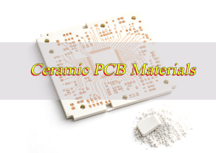
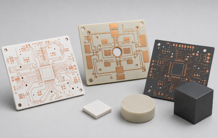
Ceramic PCB materials are inorganic ceramic substrates used as the base of printed circuit boards instead of traditional organic materials such as FR4. They are selected when a circuit must handle high heat, high voltage, high frequency, or harsh operating environments.

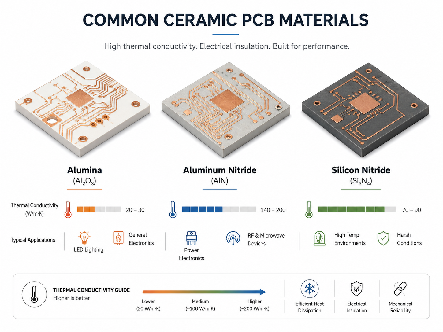
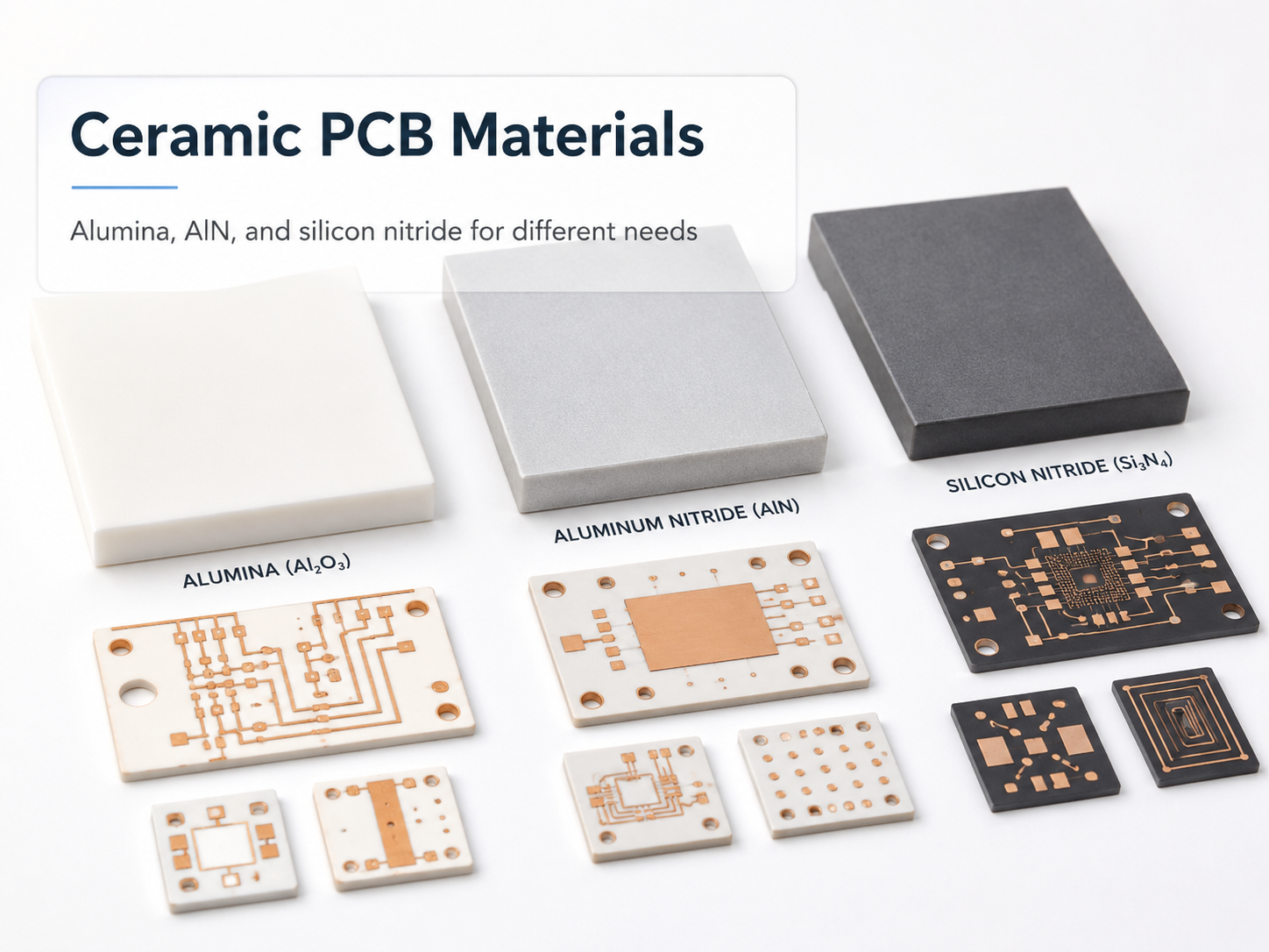
Common ceramic PCB materials include alumina (Al2O3), aluminum nitride (AlN), beryllium oxide (BeO), silicon nitride (Si3N4), and sometimes silicon carbide (SiC). These materials provide strong electrical insulation while allowing heat to move away from power devices, LEDs, RF modules, and semiconductor components.

Unlike FR4, ceramic substrates do not mainly rely on glass fiber and epoxy resin. Their performance comes from the ceramic body itself, which offers better thermal conductivity, lower thermal expansion, stronger dimensional stability, and better resistance to high-temperature operation.

For engineers and buyers, the key point is simple: ceramic PCB material is not chosen only by price. It must match heat load, circuit voltage, mechanical stress, copper thickness, assembly process, and long-term reliability requirements.

Ceramic PCB Materials, https://www.bestpcbs.com/blog/2026/06/ceramic-pcb-materials/

Why Are Ceramic PCB Materials Important?

Ceramic PCB materials are important because modern electronic products generate more heat in smaller spaces. Power modules, high-brightness LEDs, EV electronics, RF amplifiers, laser devices, and semiconductor packages all need stable heat dissipation.

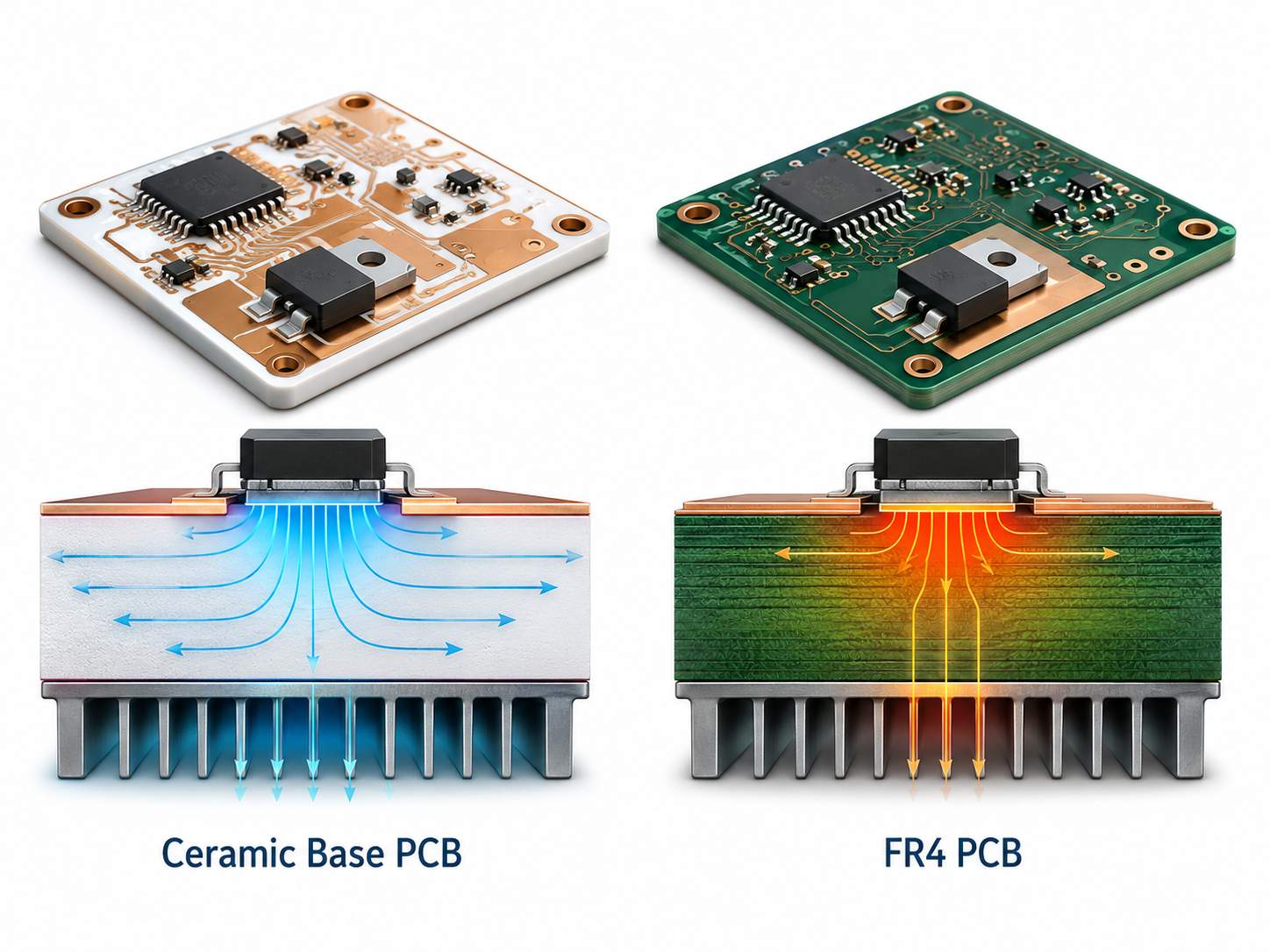
FR4 is suitable for many standard electronics, but its thermal conductivity is much lower than ceramic materials. Ceramic substrates can conduct heat far more effectively while still maintaining electrical insulation, which makes them valuable in circuits where heat cannot be allowed to accumulate around chips or solder joints.

Material choice also affects reliability. If the coefficient of thermal expansion does not match the component or copper layer, repeated heating and cooling may cause cracks, delamination, solder fatigue, or broken traces. In high-power products, this is often more serious than the initial material cost.

For procurement teams, ceramic PCB materials directly influence cost, lead time, processing difficulty, and supplier capability. A low-cost ceramic material may be enough for LED lighting, while an EV power module or high-frequency device may require AlN or another advanced ceramic substrate.

How Do Ceramic PCB Materials Work?

Ceramic PCB materials work by combining electrical insulation with thermal conduction. Most metals conduct heat well but also conduct electricity. Ceramics are different because they can transfer heat while resisting electrical current, allowing circuits to stay electrically isolated.

When a chip, LED, MOSFET, IGBT, or RF component generates heat, the ceramic substrate spreads that heat away from the component area. The heat can then move into copper layers, metal bases, housings, heat sinks, or cooling systems. This reduces hot spots and helps the device maintain stable performance.

The material structure also supports dimensional stability. Ceramic substrates usually have lower expansion than many organic PCB materials. This helps reduce mechanical stress in applications where devices repeatedly heat up and cool down.

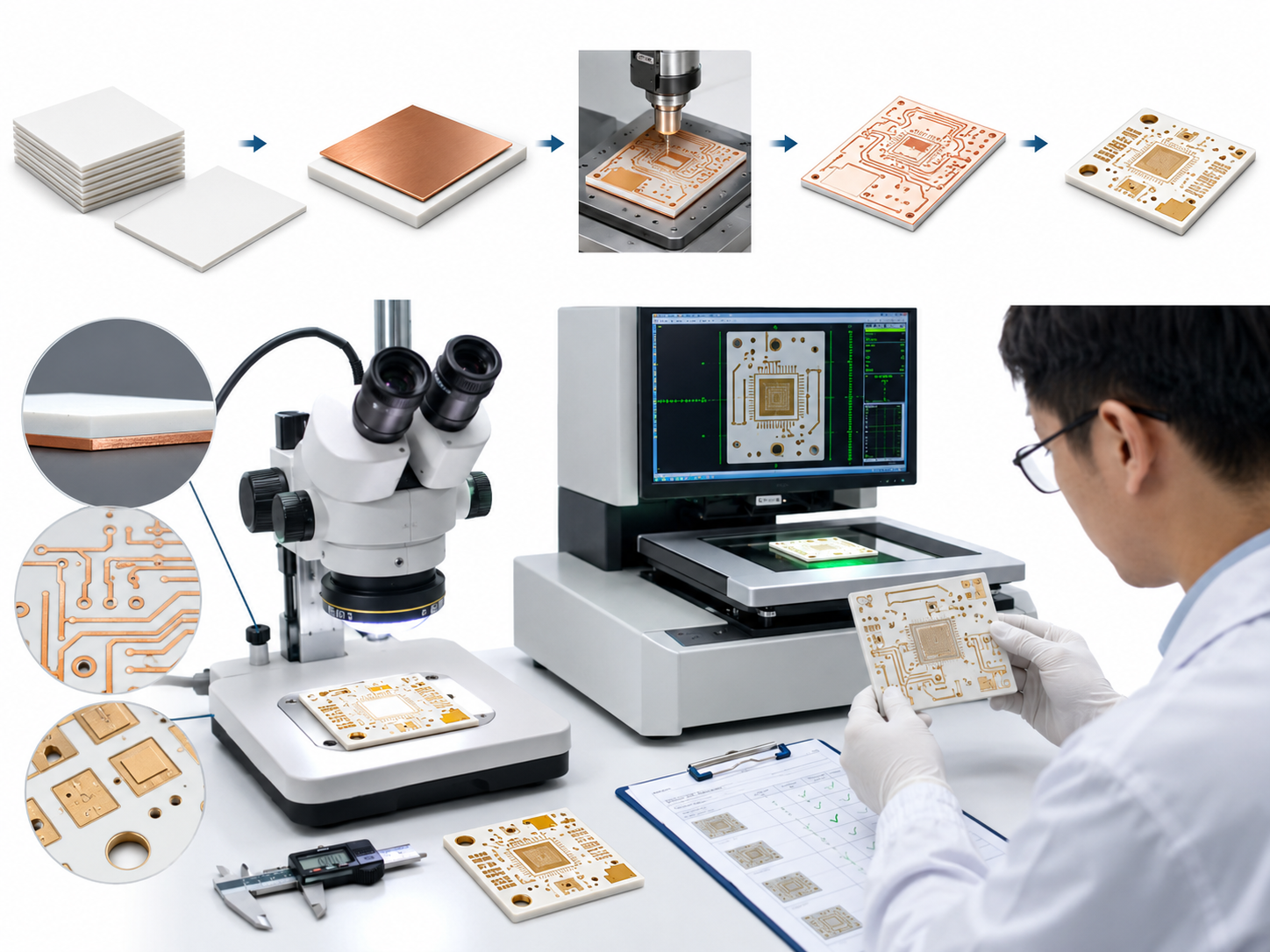
In practical manufacturing, ceramic PCB performance depends not only on the ceramic base. It also depends on metallization, copper bonding, surface finish, drilling quality, laser processing, conductor adhesion, and assembly control.

What Are the Main Types of Ceramic PCB Materials?

The main ceramic PCB materials include Al2O3, AlN, BeO, Si3N4, and SiC. Each material has a different balance of heat dissipation, insulation, strength, safety, cost, and manufacturability.

Ceramic PCB MaterialMain StrengthTypical UseSelection Note
Alumina (Al2O3)Cost-effective, stable, widely availableLEDs, sensors, power circuits, industrial electronicsGood general-purpose ceramic PCB material
Aluminum Nitride (AlN)High thermal conductivity, good insulationPower modules, semiconductor devices, RF, high-power LEDsBetter for demanding thermal management
Beryllium Oxide (BeO)Very high thermal conductivitySpecial high-power and RF applicationsRestricted by toxicity concerns during processing
Silicon Nitride (Si3N4)Strong mechanical toughness, thermal shock resistanceAutomotive, power modules, harsh environmentsUseful where mechanical reliability matters
Silicon Carbide (SiC)High-temperature capability, strong hardnessExtreme environment electronicsLess common for standard ceramic PCBs
Ceramic PCB Materials Types, https://www.bestpcbs.com/blog/2026/06/ceramic-pcb-materials/

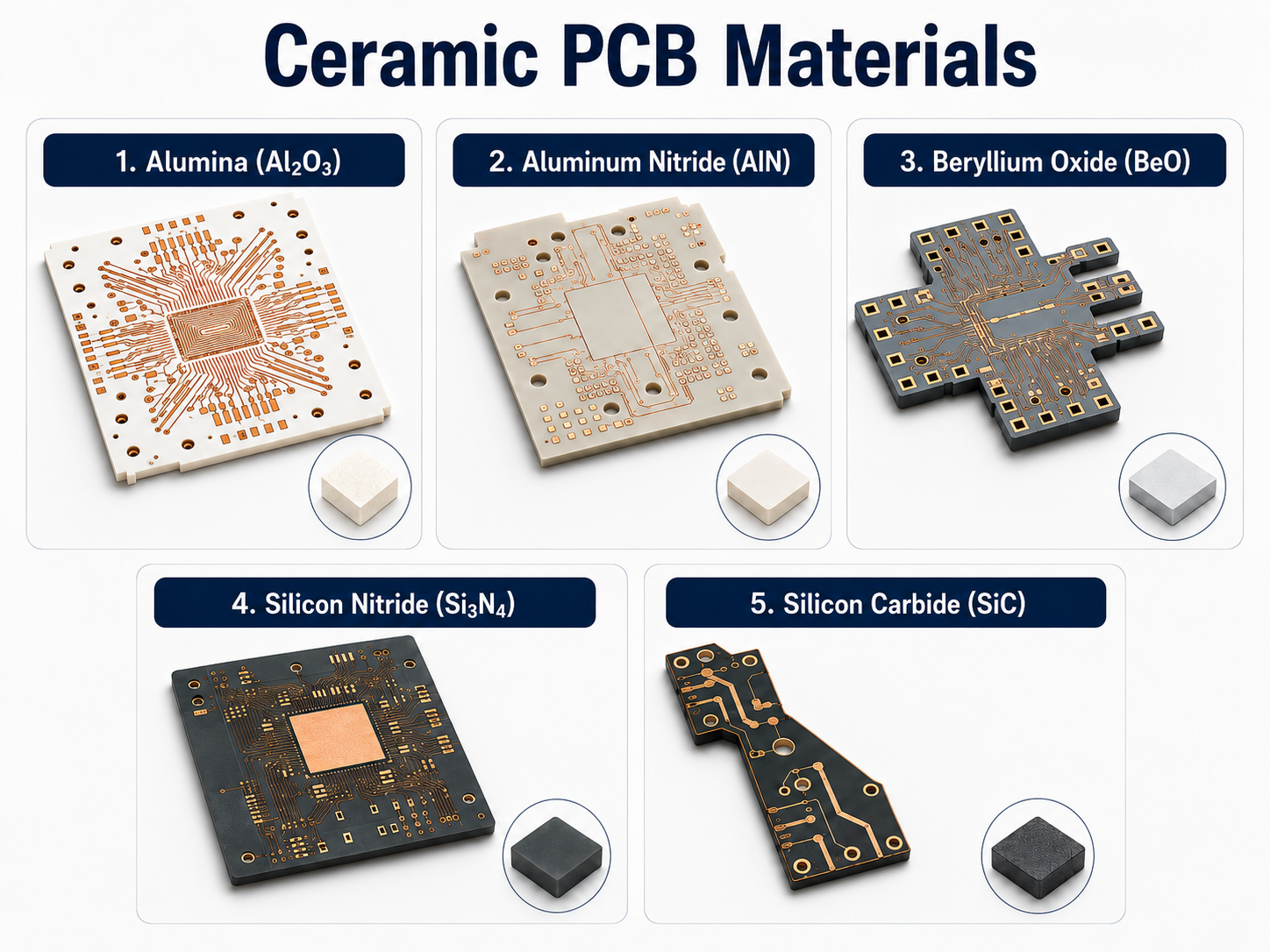
Alumina and aluminum nitride are the most common choices in many commercial ceramic PCB projects. Alumina is often selected when cost and stability matter most. Aluminum nitride is selected when high heat dissipation is the main requirement.

BeO can offer excellent thermal performance, but it requires strict safety control because of toxicity risk during machining. Many projects now prefer AlN as a safer alternative when high thermal conductivity and electrical insulation are needed.

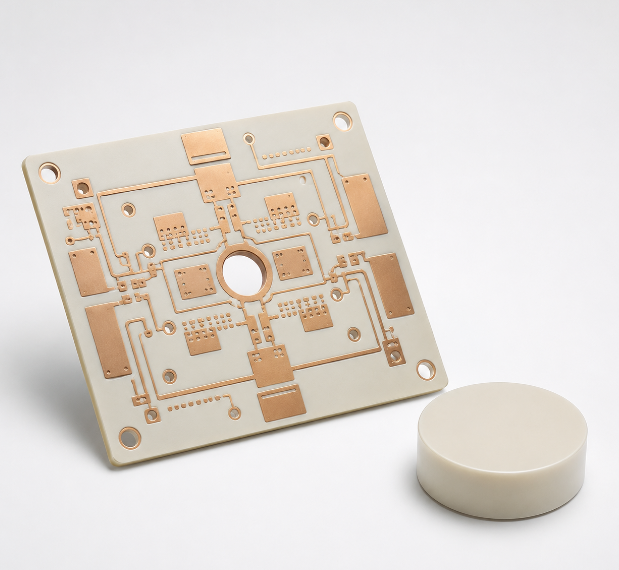
What Is Alumina Ceramic PCB Material?

Alumina ceramic PCB material, also called Al2O3 ceramic substrate, is one of the most widely used ceramic PCB materials. It offers good electrical insulation, stable mechanical performance, high-temperature resistance, and lower cost compared with many advanced ceramic substrates.

Common alumina purity levels include 96% alumina and 99.6% alumina. A 96% alumina substrate is often used for cost-sensitive ceramic PCB applications, while 99.6% alumina may be selected when better surface quality, insulation, or stability is required.

Alumina thermal conductivity is lower than AlN but still much higher than standard FR4. Many alumina ceramic substrates are commonly used in the 24–30 W/m·K thermal conductivity range, depending on purity, formulation, and processing.

Alumina ceramic PCBs are commonly used in LED modules, sensors, automotive electronics, industrial controllers, thick-film circuits, power resistors, and compact electronic modules. For many buyers, alumina is the best balance between performance, price, and production availability.

What Is Aluminum Nitride Ceramic PCB Material?

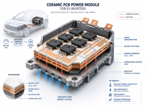
Aluminum nitride ceramic PCB material, also called AlN ceramic substrate, is selected for high thermal conductivity and electrical insulation. It is widely used in high-power electronics, semiconductor packaging, laser modules, RF devices, EV power systems, and high-brightness LED applications.

AlN is valuable because its thermal conductivity is much higher than alumina. Many commercial AlN ceramic substrates are commonly listed around 150–220 W/m·K, while actual values depend on material grade and processing quality.

Another advantage is its thermal expansion behavior. AlN has a coefficient of thermal expansion closer to silicon than many other materials, which can help reduce thermal mismatch in semiconductor-related assemblies.

The main limitation is cost. AlN is usually more expensive than alumina and may require more careful process control. However, when thermal failure risk is high, the higher material cost can be justified by better reliability and longer product life.

What Is Beryllium Oxide Ceramic PCB Material?

Beryllium oxide, or BeO, is a ceramic material known for very high thermal conductivity and good electrical insulation. It has been used in some RF, microwave, aerospace, and high-power electronic applications where heat dissipation is extremely important.

Some BeO materials can offer very strong thermal performance, which makes them attractive for demanding thermal designs. However, BeO has a major safety concern because toxic dust can be produced during machining or improper processing.

Because of this risk, many companies avoid BeO unless the application truly requires it and the supplier has proper safety systems. For many modern projects, AlN is often considered a safer alternative.

Buyers should confirm safety compliance, handling documentation, machining control, and processing capability before choosing BeO for any ceramic PCB project.

What Is Silicon Nitride Ceramic PCB Material?

Silicon nitride, or Si3N4, is a ceramic material known for high mechanical strength, fracture toughness, and thermal shock resistance. It is valuable in harsh applications where cracking risk is a major concern.

Si3N4 is often considered when the circuit must survive mechanical stress, vibration, impact, or rapid temperature cycling. This makes it attractive for automotive power modules, industrial systems, transportation electronics, and high-reliability environments.

Compared with AlN, silicon nitride may not always provide the same level of thermal conductivity. Its advantage is mechanical robustness rather than only heat dissipation.

The practical choice depends on the full design. If the biggest risk is heat, AlN may be better. If the biggest risk is mechanical stress and thermal cycling, Si3N4 may deserve serious evaluation.

How Do Alumina, AlN, BeO and Si3N4 Compare?

Different ceramic PCB materials should be compared by application needs, not by a single performance number. Thermal conductivity is important, but it is not the only selection factor.

ItemAlumina Al2O3Aluminum Nitride AlNBeryllium Oxide BeOSilicon Nitride Si3N4
Thermal conductivityMediumHighVery highMedium to high
Electrical insulationHighHighHighHigh
Mechanical toughnessMediumMediumMediumHigh
Thermal shock resistanceGoodGoodGoodExcellent
Cost levelLowerHigherHigherHigher
Processing safetyGoodGoodSpecial control neededGood
Common availabilityVery highHighLimitedMedium
Best fitGeneral ceramic PCBHigh-power thermal designSpecial high-thermal projectsHarsh mechanical environments

For most commercial projects, alumina is the practical starting point and AlN is the upgrade path for higher thermal demand. BeO is a special-case material, while Si3N4 is often chosen for strength and thermal cycling resistance.

A good supplier should not recommend the most expensive material first. The better approach is to review power density, operating temperature, copper thickness, board size, assembly method, and reliability target before confirming the substrate.

What Properties Should You Check Before Selecting Ceramic PCB Materials?

Before selecting ceramic PCB materials, engineers should check thermal, electrical, mechanical, and manufacturing parameters. These properties determine whether the substrate can survive real operating conditions.

ParameterWhy It MattersTypical Selection Focus
Thermal conductivityControls heat dissipationHigher for power modules, LEDs, RF power devices
Dielectric strengthPrevents electrical breakdownImportant for high-voltage circuits
Dielectric constantAffects signal behaviorImportant for RF and high-frequency designs
Dissipation factorAffects signal lossLower is better for RF and microwave use
Coefficient of thermal expansionControls thermal stressMust match chips, copper, and package materials
Flexural strengthAffects breakage riskImportant for handling and assembly
Surface roughnessAffects metallization and bondingImportant for fine circuits and thin film processes
Copper adhesionAffects reliabilityCritical for DBC, DPC, thick copper, and power cycling
Substrate thicknessAffects strength and thermal pathMust balance insulation, rigidity, and heat transfer
Manufacturing toleranceAffects assembly fitImportant for precision modules

For high-power applications, thermal conductivity and copper adhesion are often the first concerns. For RF applications, dielectric constant, loss tangent, and surface quality become more important.

For procurement, the most common mistake is comparing only unit price. A cheaper substrate can become expensive if it causes cracking, poor yield, solder defects, or field failure after mass production.

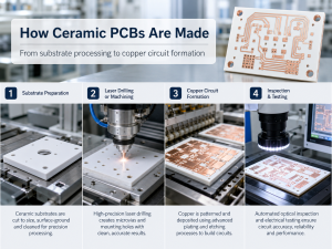
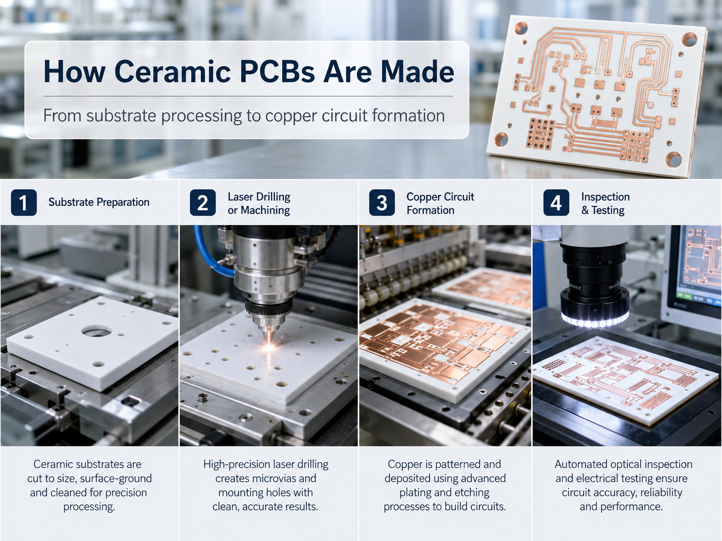
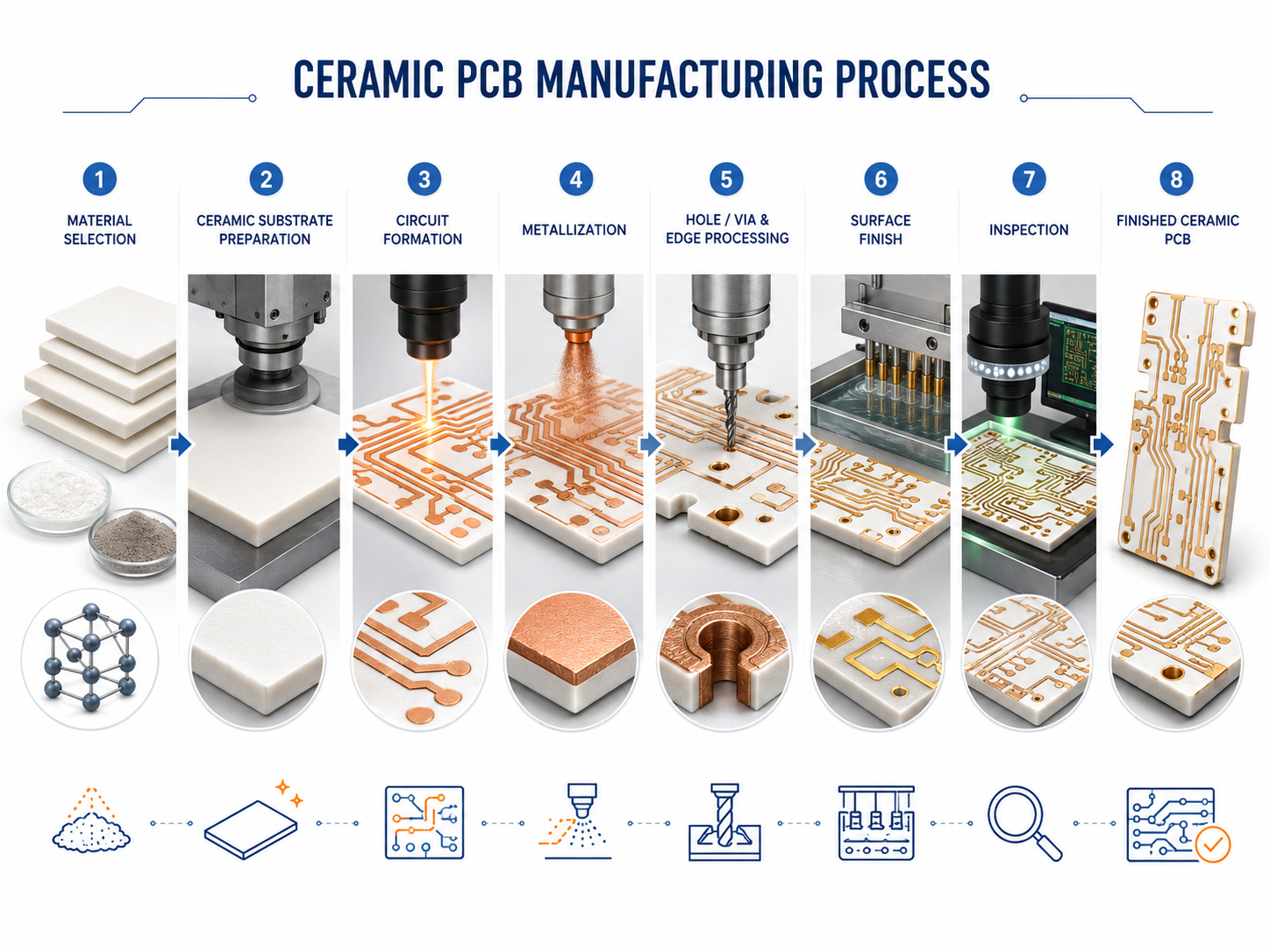
What Ceramic PCB Manufacturing Processes Use These Materials?

Ceramic PCB materials can be processed through several manufacturing methods, depending on circuit density, copper thickness, power level, and cost target.

Thick film ceramic PCB uses screen printing and firing to create conductive patterns. It is common for sensors, power resistors, hybrid circuits, and cost-sensitive ceramic electronics.

Thin film ceramic PCB uses deposition and photolithography to create fine, precise circuits. It is suitable for high-frequency, high-precision, and compact electronic modules.

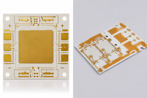
DCB ceramic PCB means direct copper bonded. It bonds copper directly to ceramic substrates and is widely used in power modules because it supports high current and strong heat dissipation.

DPC ceramic PCB means direct plated copper. It uses metallization and electroplating to build copper on ceramic. It is useful for fine circuits, LEDs, sensors, and compact high-performance modules.

LTCC and HTCC are co-fired ceramic technologies used for multilayer ceramic circuits, RF modules, microwave components, and high-reliability electronics.

What Are the Advantages of Ceramic PCB Materials?

Ceramic PCB materials offer several advantages over many traditional PCB substrates. Their biggest value is the combination of heat dissipation and insulation.

Strong thermal management allows heat to move away from chips, LEDs, and power components. This helps reduce hot spots and supports longer component life.

High electrical insulation helps ceramic PCBs support high-voltage and high-power applications without short circuits between conductive paths.

Low thermal expansion improves dimensional stability and reduces stress between chips, copper, solder joints, and the substrate during temperature cycling.

Good chemical and corrosion resistance supports use in industrial, automotive, aerospace, medical, and outdoor-related environments.

High-frequency suitability makes some ceramic materials useful in RF, microwave, antenna, telecommunications, and radar-related applications.

Ceramic PCB Materials, https://www.bestpcbs.com/blog/2026/06/ceramic-pcb-materials/

What Are the Limitations of Ceramic PCB Materials?

Ceramic PCB materials also have limitations. They are not the best choice for every circuit board project.

The first limitation is cost. Ceramic substrates are usually more expensive than FR4, especially when using AlN, Si3N4, DBC, DPC, thin film, or multilayer ceramic processes.

The second limitation is brittleness. Ceramic materials can crack under mechanical stress, improper handling, poor panel design, or fast thermal shock.

The third limitation is manufacturing complexity. Ceramic drilling, laser processing, metallization, copper bonding, and surface finishing require controlled processes. Not every standard PCB factory can produce reliable ceramic PCBs.

The fourth limitation is design flexibility. Ceramic PCBs may have restrictions in board size, hole design, edge clearance, copper thickness, and panel utilization. These constraints should be reviewed before finalizing the design.

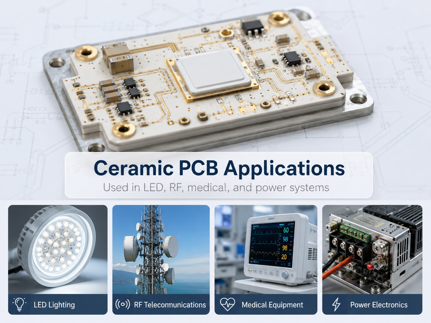
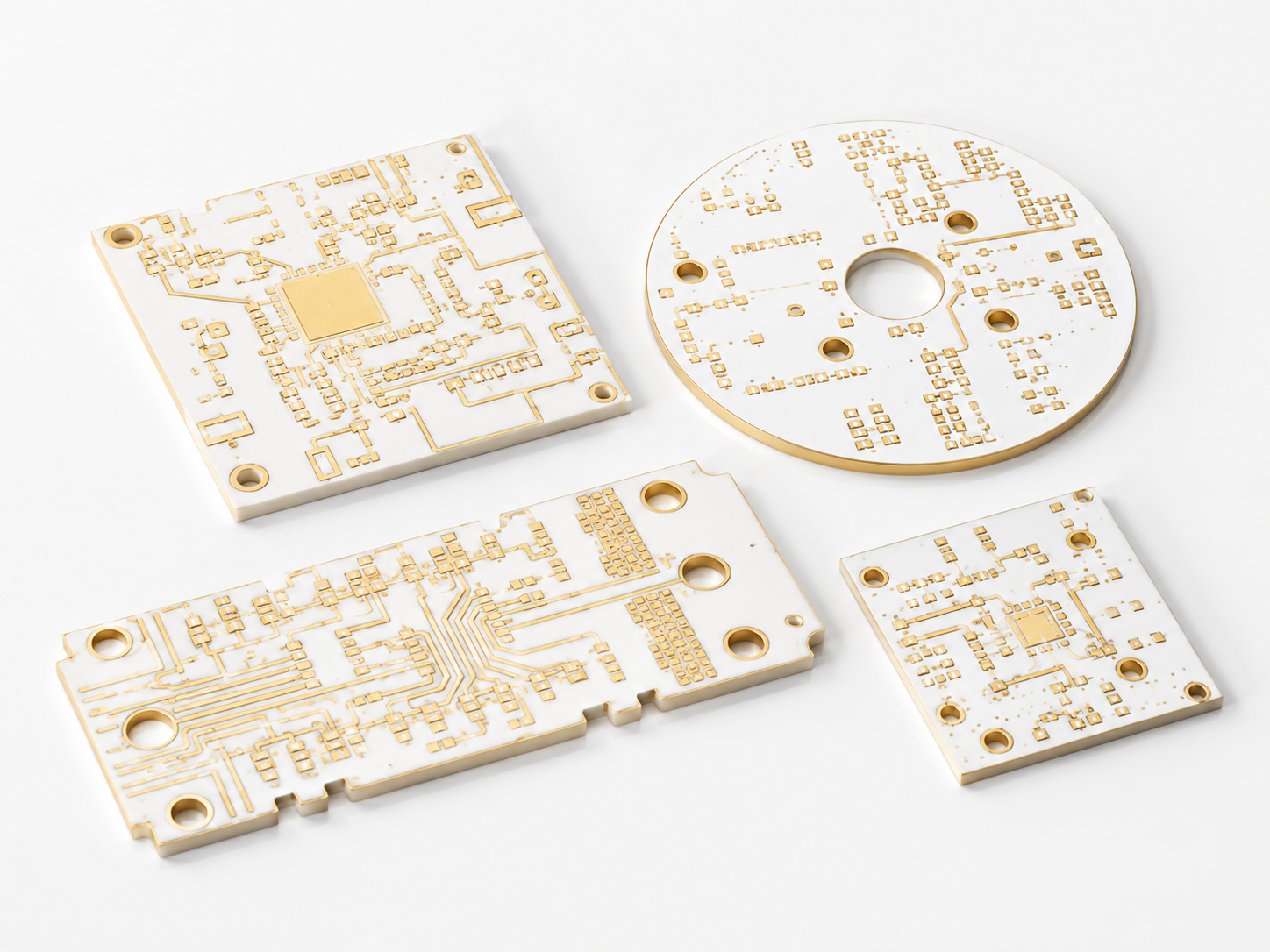
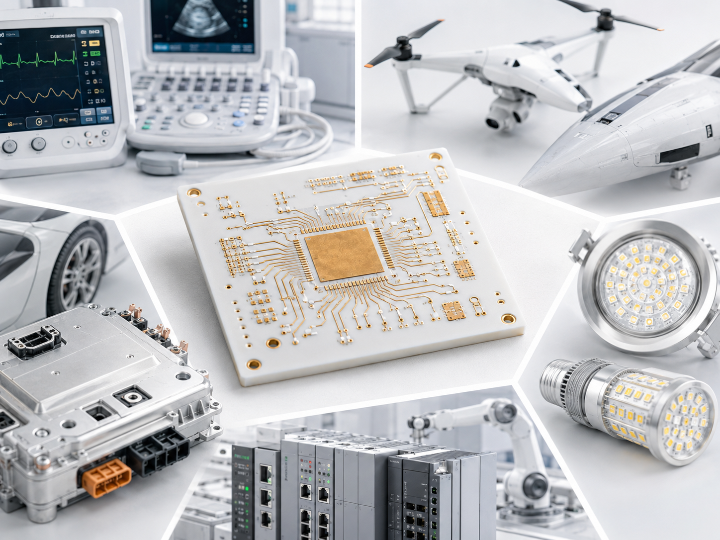
Where Are Ceramic PCB Materials Used?

Ceramic PCB materials are used in industries where heat, voltage, frequency, reliability, or harsh conditions are major design concerns.

IndustryCommon ApplicationsMaterial Focus
LED lightingHigh-power LED modules, COB LEDs, UV LEDsAlumina, AlN
Automotive electronicsEV power modules, sensors, battery systemsAlN, Si3N4, alumina
Power electronicsMOSFET, IGBT, rectifier, converter modulesAlN, DBC alumina, Si3N4
RF and microwaveRF amplifiers, antennas, microwave modulesAlumina, AlN, thin film ceramic
Medical devicesImaging systems, laser devices, precision electronicsAlumina, AlN
Aerospace and defenseHigh-reliability modules, radar, harsh environment circuitsAlN, alumina, Si3N4
TelecommunicationsRF modules, base station electronics, optical modulesAlumina, AlN
Industrial equipmentMotor drives, sensors, power control boardsAlumina, AlN

In LED projects, alumina may be enough when heat is moderate and cost control is important. In EV power modules or semiconductor devices, AlN or Si3N4 may be more suitable because thermal and reliability requirements are higher.

What Real Project Cases Show the Value of Ceramic PCB Materials?

Case 1: High-power LED module
A customer using a standard metal-core PCB may face high junction temperature in compact LED modules. By switching to an alumina or AlN ceramic substrate, heat can spread more efficiently from the LED chip area.

Case 2: EV power electronics
Power conversion circuits in EV systems face current load, heat, vibration, and repeated temperature cycling. AlN or Si3N4 ceramic substrates can help reduce thermal stress and improve module reliability.

Case 3: RF module
RF circuits require stable dielectric behavior and controlled signal loss. Alumina thin film ceramic substrates are often used where fine line accuracy and frequency stability matter.

Case 4: Industrial sensor
Industrial sensors often need compact size, stable insulation, and resistance to heat or chemicals. Alumina ceramic PCBs can provide a stable base for thick film circuits, heating elements, or sensing modules.

These cases show why material selection should start from the failure risk. If the risk is heat, choose for thermal conductivity. If the risk is cracking, choose for toughness. If the risk is signal loss, choose for dielectric performance.

What Design Factors Matter for Ceramic PCB Materials?

Designing with ceramic PCB materials requires different thinking from standard FR4 design. Ceramic substrates are strong under compression but can be fragile under bending, impact, or local stress.

Engineers should avoid sharp inside corners, weak narrow sections, and unsupported thin ceramic areas. Board outline, mounting holes, slots, and edge clearance should be designed to reduce stress concentration.

Copper thickness must also match the ceramic material and manufacturing method. Thick copper improves current capacity and heat spreading, but it can create more thermal expansion stress.

For RF circuits, trace geometry, dielectric constant, substrate thickness, surface finish, and conductor roughness must be controlled together. A ceramic material with good thermal performance may not automatically be the best RF material.

Assembly design is also important. Solder profile, component placement, thermal interface material, screw torque, and mechanical support can all affect ceramic PCB reliability after production.

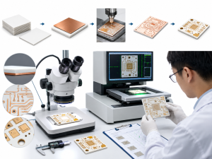
What Manufacturing Issues Should Be Controlled?

Ceramic PCB manufacturing needs strict process control because the material is hard, brittle, and sensitive to stress.

Key manufacturing issues include substrate flatness, edge chipping, laser cutting quality, hole quality, conductor adhesion, copper thickness uniformity, metallization strength, surface finish stability, and dimensional tolerance.

For DBC ceramic PCBs, copper bonding strength is critical because power cycling can stress the copper-ceramic interface. For DPC ceramic PCBs, plating quality and via reliability are important.

For thick film ceramic PCBs, paste quality, screen printing accuracy, firing temperature, conductor resistance, and pattern definition must be controlled. For thin film ceramic PCBs, surface preparation and photolithography accuracy are more important.

Buyers should ask suppliers about process capability, inspection methods, copper peel strength, thermal cycling tests, dielectric tests, and sample validation before moving into mass production.

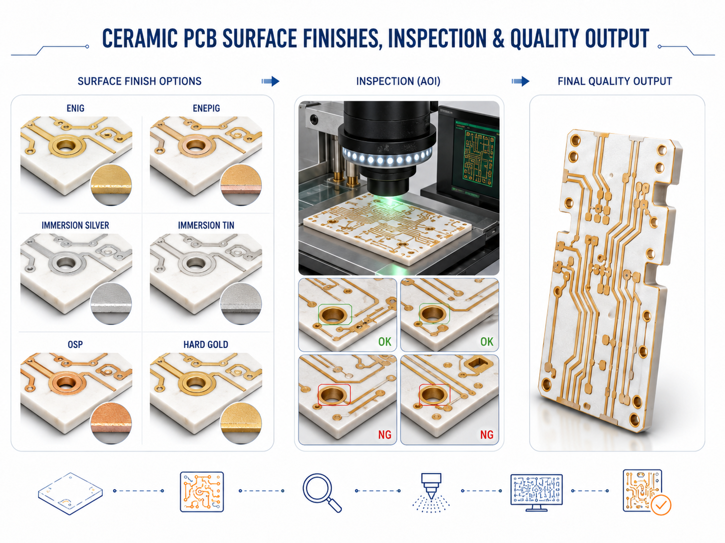
What Tests Are Needed for Ceramic PCB Materials?

Testing helps confirm whether ceramic PCB materials and manufacturing processes meet project requirements.

Test ItemPurpose
Visual inspectionChecks cracks, chips, stains, scratches, and surface defects
Dimensional inspectionConfirms size, hole position, thickness, and tolerance
Thermal conductivity reviewConfirms material grade and heat dissipation expectation
Dielectric withstand testChecks insulation under high voltage
Insulation resistance testConfirms electrical isolation
Copper adhesion testChecks bonding reliability between copper and ceramic
Thermal cycling testEvaluates stress resistance under temperature changes
Solderability testConfirms surface finish and assembly performance
Cross-section analysisReviews copper, plating, via, and interface quality
Functional testConfirms final circuit performance

For high-power products, thermal cycling and copper adhesion are especially important. For RF products, electrical performance and dimensional accuracy may be more important.

Quality control should not start after mass production. The best approach is to confirm material data, sample testing, process capability, and assembly reliability before volume orders.

What Common Failures Happen with Ceramic PCB Materials?

Common ceramic PCB failures include cracking, copper delamination, solder joint fatigue, insulation breakdown, hot spots, edge chipping, and poor conductor adhesion.

Cracking often happens when mechanical stress is not controlled. Causes may include poor panel design, excessive screw torque, improper handling, fast thermal shock, or unsupported mounting.

Copper delamination can happen when the bonding process is weak or when copper thickness, thermal cycling, and material expansion are not properly matched.

Solder fatigue may occur when ceramic, copper, component package, and solder joints expand at different rates during repeated heating and cooling.

Insulation breakdown may happen if voltage clearance, contamination control, dielectric strength, or surface cleanliness is not properly managed.

Hot spots usually come from poor thermal path design. Even a high-performance ceramic material cannot solve heat problems if component placement, copper area, thermal vias, or heat sink contact are poorly designed.

How Should You Choose the Right Ceramic PCB Material?

The right ceramic PCB material should be selected by matching the material to the project’s main risk.

Choose alumina if the project needs stable insulation, moderate thermal performance, good availability, and lower cost. It is suitable for many LED, sensor, industrial, and general ceramic circuit applications.

Choose AlN if the project has high heat density, power semiconductors, compact LED modules, laser devices, or semiconductor packages. It is better when thermal management is the main concern.

Choose Si3N4 if the project must survive vibration, mechanical stress, and repeated thermal shock. It is useful in automotive and harsh-environment power modules.

Choose BeO only when very high thermal conductivity is required and the supplier can properly manage safety, machining, and compliance risks.

The safest selection method is to provide your supplier with operating temperature, power load, voltage, current, copper thickness, board size, surface finish, assembly process, and reliability test requirements before final material confirmation.

What Affects the Cost of Ceramic PCB Materials?

Ceramic PCB cost is affected by substrate material, purity, thickness, copper thickness, circuit complexity, processing method, surface finish, tolerance, order quantity, and testing requirements.

Alumina is usually more cost-effective than AlN. AlN costs more because of material price and processing requirements, but it may reduce thermal failure risk in demanding applications.

DBC and DPC ceramic PCBs also differ in cost. DBC is often used for high-current and power modules, while DPC can support finer features but may require more processing steps.

Thin film ceramic PCBs are usually more expensive than thick film ceramic PCBs because they require higher precision and more controlled processes.

Testing and quality requirements also affect price. Thermal cycling, dielectric testing, cross-section analysis, and special reliability validation increase cost, but they are often necessary for automotive, medical, aerospace, and high-power applications.

How Can Buyers Evaluate a Ceramic PCB Material Supplier?

Buyers should evaluate a ceramic PCB supplier by material capability, process experience, engineering support, quality control, and mass production stability.

A qualified supplier should clearly explain the difference between alumina, AlN, BeO, Si3N4, DBC, DPC, thick film, and thin film ceramic PCB options. If the supplier only quotes price without reviewing application conditions, the project may face hidden reliability risks.

Important supplier questions include:

  • What ceramic materials can you process?
  • What substrate thickness and copper thickness can you support?
  • Can you provide DBC, DPC, thick film, or thin film options?
  • What are your standard tolerances?
  • How do you inspect cracks, edge chips, and copper adhesion?
  • Can you support prototype and mass production?
  • What reliability tests can you provide?
  • Can you review design risks before production?

For overseas buyers, the supplier should also support clear technical communication, stable lead time, export documentation, RoHS-related compliance, and practical packaging protection for brittle ceramic boards.

What Should You Confirm Before Ordering Ceramic PCB Materials?

Before ordering ceramic PCB materials, confirm both technical and commercial details. This reduces sample failure, quotation misunderstanding, and mass production delay.

Checklist ItemWhat to Confirm
Material typeAlumina, AlN, BeO, Si3N4, or other ceramic
Material gradePurity, thermal conductivity, dielectric properties
Board thicknessMechanical strength and insulation requirement
Copper thicknessCurrent capacity and thermal spreading
Manufacturing processDBC, DPC, thick film, thin film, LTCC, HTCC
Surface finishENIG, silver, nickel, gold, or project-specific finish
ToleranceOutline, holes, copper pattern, flatness
Assembly methodSMT, wire bonding, soldering, sintering, module assembly
TestingElectrical, thermal, adhesion, reliability, visual inspection
Quantity planPrototype, pilot run, mass production
PackagingAnti-crack protection during shipping
DocumentationDrawing, Gerber, stack-up, material data, inspection report
ceramic PCB material, https://www.bestpcbs.com/blog/2026/06/ceramic-pcb-materials/

For new projects, prototype validation is strongly recommended before mass production. Ceramic PCB mistakes are usually more expensive to correct after tooling, metallization, or assembly has already started.

FAQs About Ceramic PCB Materials

Q1: What are the most common ceramic PCB materials?
A1: The most common ceramic PCB materials are alumina and aluminum nitride. Alumina is widely used because it is stable, cost-effective, and available. Aluminum nitride is used when stronger heat dissipation is required. BeO, Si3N4, and SiC are used in more specialized applications.

Q2: Is alumina or aluminum nitride better for ceramic PCBs?
A2: Neither is always better. Alumina is better for cost-sensitive and general ceramic PCB applications. Aluminum nitride is better for high-power, high-heat, and semiconductor-related designs. The right choice depends on thermal load, budget, circuit structure, and reliability targets.

Q3: Why are ceramic PCB materials better than FR4 for heat dissipation?
A3: Ceramic materials conduct heat much better than FR4 while keeping electrical insulation. This helps move heat away from power devices, LEDs, RF components, and semiconductor chips. For high-power circuits, this can reduce hot spots and improve long-term stability.

Q4: What is the thermal conductivity of alumina ceramic PCB material?
A4: Alumina ceramic PCB material is often listed around 24–30 W/m·K, depending on purity and formulation. It is lower than AlN but much higher than standard FR4, making it suitable for LEDs, sensors, industrial electronics, and general thermal applications.

Q5: What is the thermal conductivity of AlN ceramic PCB material?
A5: Commercial AlN ceramic substrates are often listed around 150–220 W/m·K, with values depending on material grade and processing quality. AlN is commonly selected for power electronics, semiconductor modules, laser devices, and high-brightness LED systems.

Q6: Are ceramic PCB materials electrically conductive?
A6: Most ceramic PCB substrates are electrical insulators. Their value comes from conducting heat while resisting electrical current, allowing ceramic PCBs to support high-power circuits safely. This makes them useful for power modules, LEDs, RF devices, and high-voltage electronics.

Q7: Can ceramic PCB materials crack easily?
A7: Ceramic materials can crack if they are exposed to bending, impact, excessive screw pressure, sharp design corners, or fast thermal shock. Good design, proper handling, controlled assembly, and protective packaging can help reduce cracking risk.

Q8: What is DBC ceramic PCB material used for?
A8: DBC ceramic PCB is commonly used in high-current and high-power modules. It bonds copper directly to ceramic substrates, creating strong heat dissipation and current-carrying capability. It is often used in EV electronics, converters, power modules, and industrial control systems.

Q9: What is DPC ceramic PCB material used for?
A9: DPC ceramic PCB is useful when finer circuits, good thermal performance, and compact design are needed. It is often used in LED modules, sensors, power devices, and precision electronic products where circuit accuracy and thermal control are both important.

Q10: Are ceramic PCB materials suitable for RF applications?
A10: Yes, some ceramic PCB materials are suitable for RF and microwave applications. For RF design, engineers must check dielectric constant, loss, surface quality, and conductor accuracy. Alumina and AlN are common choices for many high-frequency ceramic circuit designs.

Q11: Why is AlN often used in power electronics?
A11: AlN is used in power electronics because it provides high thermal conductivity and good electrical insulation. It helps move heat away from power chips and reduces thermal stress when matched with suitable copper thickness, package structure, and assembly process.

Q12: Is BeO still used in ceramic PCBs?
A12: BeO is still used in some special high-thermal applications, but it requires strict safety control. Many companies prefer AlN when they need strong thermal performance with fewer safety concerns. Buyers should confirm safety documentation before choosing BeO.

Q13: How do I choose ceramic PCB material for LED applications?
A13: For standard LED applications, alumina may be enough. For high-power LEDs, UV LEDs, COB modules, or compact lighting systems with higher heat density, AlN may be a better choice. The final selection should match power, heat, size, and cost requirements.

Q14: What files are needed for a ceramic PCB quotation?
A14: A supplier usually needs Gerber files, drawings, material requirements, board thickness, copper thickness, surface finish, quantity, tolerance, assembly requirements, and testing needs. If the material is uncertain, provide operating temperature, voltage, current, and application details.

Q15: Can ceramic PCBs be customized for OEM or ODM projects?
A15: Yes, ceramic PCBs can be customized for OEM and ODM projects. Custom options may include substrate material, thickness, copper thickness, surface finish, outline, hole structure, metallization method, testing standard, and packaging method. This helps match the board to real product requirements.

Summary

Ceramic PCB materials are selected when a circuit needs better heat dissipation, electrical insulation, high-temperature stability, and long-term reliability than standard organic PCB materials can provide. Alumina is often the practical choice for cost-effective ceramic PCB projects, while aluminum nitride is preferred for high-power and high-thermal applications. BeO, Si3N4, and SiC are more specialized materials for demanding environments.

For material selection, engineers should not compare only thermal conductivity or price. The better decision comes from reviewing power density, voltage, copper thickness, thermal cycling, mechanical stress, manufacturing process, assembly method, and reliability testing. Buyers should also confirm supplier experience with ceramic processing, copper adhesion, crack control, inspection, packaging, and mass production support.

You may also like

Ceramic Base PCB: How to Choose?
Thursday, May 28th, 2026

Ceramic base PCB is used when a circuit board must manage heat, electrical insulation, dimensional stability, or high-frequency performance better than a standard organic substrate. In many power, LED, RF, automotive, medical, and industrial products, the PCB is not only a carrier for components. It also becomes part of the thermal path and reliability design.

Ceramic Base PCB: How to Choose?

EBest Circuit (Best Technology) provides ceramic PCB fabrication, PCB manufacturing, component sourcing, PCBA assembly, DFM support, and testing for projects from prototypes to production.

What Is a Ceramic Base PCB?

Ceramic base PCB is a printed circuit board that uses a ceramic substrate as the main insulating base. Instead of glass-reinforced epoxy, it uses materials such as alumina, aluminum nitride, silicon nitride, or other ceramic substrates. Copper circuits are formed on the ceramic surface through processes such as DPC, DBC, AMB, thick film, or thin film technology.

The ceramic base supports both mechanical and electrical functions. It carries copper traces and components, provides insulation between conductive paths, and helps transfer heat away from active devices. This is why ceramic PCB is often used in high-power and high-reliability products.

A ceramic PCB board may be single-sided, double-sided, or multilayer. Simple LED modules may only require a single-sided structure. Power modules may need thick copper and strong bonding. RF circuits may require stable dielectric properties and controlled impedance.

In sourcing, buyers may use several related terms, such as ceramic PCB board, ceramic base, or even ceramics base. The key is to confirm the actual material, copper thickness, surface finish, tolerance, operating temperature, and assembly requirements before quotation.

Ceramic base PCB is commonly used for high-power LEDs, MOSFETs, IGBTs, laser diodes, RF power amplifiers, sensors, and compact power modules. These devices often generate concentrated heat. A ceramic substrate helps move that heat from the component area to the external cooling structure.

How Is a Ceramic Base PCB Different from a Standard FR4 PCB?

Ceramic base PCB and an FR4 PCB can both carry components and copper circuits, but their substrate materials are different. FR4 uses glass fiber and epoxy resin. Ceramic PCB uses inorganic ceramic material. This difference affects thermal conductivity, temperature resistance, insulation, cost, and manufacturing method.

FR4 is suitable for many standard electronic products because it is economical, mature, and easy to process. It is widely used in consumer electronics, industrial control boards, communication products, and general PCBA projects.

Ceramic Base PCB: How to Choose?

Ceramic PCB is selected when FR4 cannot meet the thermal, electrical, or environmental requirements. It is more common in power electronics, LED modules, RF circuits, semiconductor packaging, automotive electronics, and medical devices.

ItemCeramic Base PCBStandard FR4 PCB
Base materialAlumina, aluminum nitride, silicon nitride, or other ceramic materialGlass fiber reinforced epoxy
Thermal conductivityCommonly about 20–230 W/m·K, depending on materialCommonly about 0.3–0.5 W/m·K
Heat dissipationTransfers heat through the ceramic substrateUsually relies on thermal vias, copper planes, heat sinks, or metal core design
Temperature stabilitySuitable for high-temperature environmentsSuitable for general electronics
Electrical insulationHigh dielectric strengthGood insulation for standard circuits
Dimensional stabilityStable under temperature changeMore affected by thermal expansion and moisture
Processing costHigherLower
Typical usePower modules, LEDs, RF circuits, sensors, automotive, medicalGeneral electronics, control boards, digital circuits, consumer products

The main difference is not only heat dissipation. Ceramic PCB also offers stable electrical behavior, low moisture absorption, and good mechanical stability. These features are useful when the product must work in a compact structure or demanding environment.

Manufacturing is also different. FR4 can be drilled, laminated, plated, routed, and assembled through mature PCB processes. Ceramic is harder and more brittle, so it needs controlled cutting, laser processing, metallization, copper bonding, and careful handling during assembly.

Why Are Ceramic Materials Used as a PCB Base?

Ceramic materials are used as a PCB base because they combine thermal conductivity and electrical insulation. This combination is important for circuits that must move heat away from components without creating electrical leakage or short-circuit risk.

In power electronics, heat usually comes from semiconductor devices, resistors, LEDs, or power ICs. If heat remains near the component, the product may lose efficiency, reduce output stability, or shorten service life. A ceramic base helps create a direct thermal path from the component to the substrate and then to the heat sink or housing.

Ceramic materials also maintain stable performance under high temperature. They have low moisture absorption, good chemical resistance, and reliable dimensional stability. These properties make them useful in industrial, automotive, energy, medical, and aerospace electronics.

For RF and microwave circuits, ceramic PCB materials can also provide stable dielectric properties. This helps engineers control impedance, signal loss, and phase behavior. In antennas, filters, radar modules, and RF power devices, substrate stability directly affects circuit performance.

Main reasons to use ceramic materials as a PCB base include:

  • Better heat transfer than FR4
  • High electrical insulation
  • Stable dielectric properties
  • Low moisture absorption
  • Good dimensional stability
  • Suitability for compact power designs
  • Stable behavior under high temperature

Ceramic is not selected only because it is a premium material. It is selected when the design requires thermal, electrical, or mechanical performance that standard PCB materials cannot provide efficiently.

What Ceramic PCB Materials Are Commonly Used?

Common ceramic PCB materials include alumina, aluminum nitride, silicon nitride, and beryllium oxide. Each material has different thermal conductivity, mechanical behavior, process difficulty, and cost.

Alumina, also called Al₂O₃, is the most widely used ceramic PCB material. It offers good insulation, acceptable thermal conductivity, mature manufacturing support, and a practical ceramic board price. Common grades include 96% alumina and 99.6% alumina. For many LED, sensor, and industrial applications, alumina provides a balanced solution.

Aluminum nitride, also called AlN, is used when heat dissipation is a main requirement. It has much higher thermal conductivity than alumina and has a thermal expansion coefficient closer to silicon. This makes it suitable for high-power LEDs, laser modules, semiconductor packages, and compact power modules.

Silicon nitride, or Si₃N₄, is known for mechanical strength and thermal shock resistance. It is often used in automotive power modules and reliability-focused power electronics. It is useful when the design must handle temperature cycling, vibration, or mechanical stress.

Ceramic Base PCB: How to Choose?

Beryllium oxide, or BeO, has high thermal conductivity, but it requires strict safety control during processing. Because of handling concerns, many projects use aluminum nitride as an alternative when high thermal conductivity is required.

MaterialTypical Thermal ConductivityMain FeaturesCommon Applications
Alumina / Al₂O₃About 20–30 W/m·KMature process, good insulation, controlled costLEDs, sensors, industrial electronics, general ceramic PCB
Aluminum Nitride / AlNAbout 170–230 W/m·KHigh thermal conductivity, good semiconductor compatibilityHigh-power LEDs, laser modules, power modules
Silicon Nitride / Si₃N₄About 60–90 W/m·K depending on gradeHigh mechanical strength, thermal shock resistanceAutomotive power electronics, high-reliability modules
Beryllium Oxide / BeOAbout 200–300 W/m·KHigh thermal conductivity, special handling requirementsSpecialized RF and power applications

Material selection should match the working conditions. Alumina is often suitable for cost-sensitive applications with moderate heat. Aluminum nitride is used when thermal conductivity is critical. Silicon nitride is useful when mechanical reliability is a priority.

A reliable ceramic base PCB manufacturer should not recommend material based only on performance data. It should also consider cost, manufacturability, lead time, copper structure, surface finish, and assembly method.

How Does a Ceramic Base PCB Help with Heat Dissipation?

A ceramic base PCB helps with heat dissipation by forming a shorter and more efficient thermal path between heat-generating components and the external cooling structure. Heat can move from the component pad into the copper layer, through the ceramic substrate, and then into the heat sink, metal housing, or thermal interface material.

In a standard FR4 PCB, heat transfer through the substrate is limited. Engineers often add thermal vias, large copper planes, heat sinks, or metal core structures to improve thermal performance. These methods can work well, but they may require more board space and more design control.

Ceramic substrates have higher thermal conductivity, so they can transfer heat more directly through the board. This is useful in compact power circuits where heat is concentrated in a small area.

Substrate TypeTypical Thermal ConductivityDesign Meaning
FR4About 0.3–0.5 W/m·KSuitable for general circuits; needs additional thermal design for higher power
Aluminum PCB dielectric layerOften about 1–3 W/m·KUseful for LED and power boards, but dielectric layer affects heat transfer
Alumina ceramicAbout 20–30 W/m·KSuitable for moderate to high thermal needs
Aluminum nitride ceramicAbout 170–230 W/m·KSuitable for high-power and compact thermal designs
Silicon nitride ceramicAbout 60–90 W/m·K depending on gradeSuitable when heat transfer and mechanical strength are both important

Copper thickness also affects thermal behavior. Thick copper helps spread heat across the surface. Ceramic helps conduct heat through the substrate. When these two functions are combined properly, the PCB can support higher power density.

Substrate thickness should also be reviewed. A thinner ceramic substrate can reduce thermal resistance, but it must still meet insulation and mechanical strength requirements. A thicker substrate may improve handling strength, but it can increase the thermal path length.

For LED modules, ceramic PCB helps control junction temperature. This supports stable brightness, color performance, and operating life. For power semiconductors, better heat transfer helps reduce thermal stress and improves operating stability.

What Are the Main Benefits of Ceramic Base PCBs?

Ceramic base PCBs provide thermal, electrical, and mechanical advantages for applications that require more than standard PCB performance. Their main value is the ability to conduct heat while maintaining insulation.

The first benefit is thermal conductivity. Ceramic substrates transfer heat more efficiently than FR4. This helps high-power components work within a more controlled temperature range.

The second benefit is electrical insulation. Ceramic materials can provide high dielectric strength while still allowing heat to pass through the substrate. This is useful for power modules, LED arrays, high-voltage circuits, and compact electronics.

The third benefit is dimensional stability. Ceramic substrates expand less than many organic materials under temperature change. This helps maintain circuit accuracy and solder joint stability.

The fourth benefit is environmental stability. Ceramic materials have low moisture absorption and good resistance to many chemicals. This is useful in industrial, automotive, medical, and outdoor applications.

Main benefits include:

  • High thermal conductivity for power-dense designs
  • Good electrical insulation for high-voltage circuits
  • Stable size under temperature change
  • Low moisture absorption
  • Suitable for high-temperature environments
  • Good compatibility with compact modules
  • Stable dielectric behavior for RF designs

Ceramic base PCB is especially useful when thermal management, insulation, and reliability must be handled in the same structure. It can also reduce dependence on large external cooling designs when the product structure allows a direct thermal path.

What Applications Use Ceramic Base PCBs?

Ceramic base PCBs are used in products that require heat dissipation, insulation, compact size, stable signal behavior, or long-term reliability. They are common in LED lighting, power electronics, RF modules, automotive electronics, medical devices, aerospace systems, and sensor modules.

Application AreaCommon UseWhy Ceramic Is Used
LED lightingHigh-power LED, UV LED, automotive lightingHeat dissipation and compact structure
Power electronicsInverters, converters, MOSFET and IGBT modulesThermal transfer and insulation
RF and microwaveAntennas, filters, radar modules, amplifiersStable dielectric properties
AutomotiveEV power units, lighting, sensorsThermal cycling and reliability
Medical electronicsSensors, imaging modules, compact power circuitsStability and process control
Aerospace and UAVRF modules, power control, sensorsWeight, heat, and reliability considerations

EBest Circuit (Best Technology) supports ceramic PCB projects for customers in lighting, industrial control, communication, medical, automotive, and power electronics fields. For these projects, early review of material, copper thickness, thermal path, and assembly method helps improve manufacturability.

How Is a Ceramic Base PCB Manufactured?

Ceramic base PCB manufacturing depends on the substrate material and copper formation process. The main production steps include ceramic substrate preparation, cleaning, metallization, copper formation, circuit patterning, surface finishing, inspection, and profiling.

The process starts with ceramic substrate selection. The factory checks material type, thickness, flatness, surface quality, and dimensional tolerance. A clean and stable surface is important because copper adhesion depends on the substrate condition.

The next step is copper formation or metallization. Different methods are used depending on the design requirement.

DPC, or Direct Plated Copper, uses sputtering and electroplating to form copper on ceramic. It is suitable for fine lines, compact layouts, and precise circuit structures.

DBC, or Direct Bonded Copper, bonds copper foil directly to ceramic at high temperature. It is often used for power electronics because it supports thick copper and higher current capacity.

AMB, or Active Metal Brazing, uses active brazing material to bond copper and ceramic. It is used for high-reliability power modules that require strong bonding.

Thick film technology prints conductive paste on ceramic and fires it at high temperature. It is often used in hybrid circuits and ceramic electronic modules.

Thin film technology forms very fine and accurate circuit patterns. It is suitable for precision applications where tight feature control is required.

Ceramic Base PCB: How to Choose?

A typical process flow includes:

  • Ceramic substrate inspection
  • Surface cleaning and preparation
  • Copper bonding or metallization
  • Circuit imaging and etching
  • Plating and surface finish
  • Laser cutting, drilling, or profiling
  • Electrical testing and visual inspection
  • Dimensional and surface quality check

Design rules vary by process. DPC can support finer features, while DBC is better for thick copper and high-current designs. AMB is selected when bonding strength and reliability are important. The correct process should be chosen based on copper thickness, line width, current load, thermal requirement, and cost target.

What Affects Ceramic PCB Cost?

Ceramic PCB cost is affected by material type, substrate size, ceramic thickness, copper thickness, circuit complexity, surface finish, process type, tolerance, testing, quantity, and assembly requirements. When evaluating ceramic board price, the complete specification is more important than board size alone.

Material is a major factor. Alumina is usually more cost-effective and suitable for many standard ceramic PCB applications. Aluminum nitride costs more because it provides much higher thermal conductivity and requires more controlled processing. Silicon nitride may also cost more due to its mechanical properties and specialized applications.

Copper thickness affects both material usage and process difficulty. Thick copper supports higher current and better heat spreading, but it requires more process control during bonding, etching, and inspection.

Circuit complexity also affects cost. Fine lines, tight spacing, small holes, special shapes, and tight tolerances require more precise production. Surface finish can also change cost, especially when the design requires ENIG, silver, gold, or wire-bondable finishes.

Cost FactorEffect on PricePractical Note
Ceramic materialAlN and Si₃N₄ usually cost more than aluminaSelect material based on actual thermal and mechanical needs
Substrate thicknessNon-standard thickness may increase costUse standard thickness when possible
Copper thicknessThick copper increases material and process costMatch copper to current and heat requirements
Process typeDPC, DBC, AMB, thick film, and thin film have different cost levelsChoose process based on performance and manufacturability
Circuit complexityFine features and tight tolerances increase production difficultyKeep layout practical for the selected process
Surface finishSpecial finishes add costDefine soldering or bonding requirements clearly
QuantitySmall batches have higher unit costUse prototypes for validation, then optimize batch production
Testing and documentationExtra inspection increases cost but improves controlSpecify only required test items

To control ceramic PCB cost, avoid unnecessary over-specification. For example, aluminum nitride may not be required if alumina already meets the thermal target. Very thick copper may not be useful if the current load is moderate. A DFM review can help identify these issues before production.

EBest Circuit (Best Technology) can review ceramic PCB designs before manufacturing. This helps confirm material selection, copper structure, surface finish, panel use, and assembly feasibility. For ceramic PCB projects, early engineering review can improve cost control and production stability.

How Do You Choose a Reliable Ceramic Base PCB Factory?

To choose a reliable ceramic base PCB factory, evaluate its material knowledge, process capability, DFM support, inspection system, traceability, PCBA support, and communication quality. Ceramic PCB production is more specialized than standard FR4 PCB fabrication, so the supplier should understand the design purpose, not only the Gerber files.

First, check material capability. A qualified ceramic base PCB manufacturer should understand alumina, aluminum nitride, silicon nitride, copper thickness options, substrate thickness, thermal conductivity, dielectric properties, and surface finish choices. The supplier should help match the material to heat, voltage, mechanical stress, frequency, and budget.

Second, check process capability. Confirm whether the factory supports DPC, DBC, AMB, thick film, thin film, or the specific ceramic process required by your design. Also check minimum trace and spacing, copper thickness range, hole processing, outline tolerance, and available surface finishes.

Third, check engineering support. Ceramic PCB often needs DFM review before production. The factory should review copper-to-edge spacing, pad design, thermal path, substrate thickness, panelization, soldering method, and assembly handling.

Fourth, check quality control. Useful inspection items include electrical testing, visual inspection, dimensional measurement, copper thickness measurement, adhesion testing, surface finish inspection, and material traceability. For medical, automotive, industrial, or aerospace products, documentation control is also important.

Selection PointWhat to Check
Material knowledgeAlumina, AlN, Si₃N₄, substrate thickness, thermal conductivity
Process capabilityDPC, DBC, AMB, thick film, thin film, copper thickness
DFM supportLayout review, thermal path review, pad design, manufacturability
Quality controlE-test, dimensional inspection, adhesion check, surface finish control
TraceabilityMaterial batch, process records, inspection data
PCBA supportSMT assembly, component sourcing, testing, fixture support
CommunicationClear quotation, technical feedback, delivery updates

EBest Circuit (Best Technology) supports ceramic PCB fabrication, PCB manufacturing, component sourcing, SMT assembly, testing, and one-stop PCBA production. This is useful when the ceramic PCB is part of a complete module and requires coordination between bare board fabrication and assembly.

Before requesting a quotation, prepare Gerber files, drill files, outline drawings, material requirements, substrate thickness, copper thickness, surface finish, quantity, operating temperature, voltage, current load, thermal target, and assembly notes. If the material has not been finalized, provide the application background so the factory can recommend a practical option.

To summarize, ceramic base PCB is suitable for designs that require better heat dissipation, electrical insulation, dimensional stability, and reliability than standard FR4 can provide. Alumina is often used for balanced cost and performance, aluminum nitride is used for high thermal conductivity, and silicon nitride is suitable for mechanically demanding applications. For ceramic base PCB fabrication, ceramic PCB board manufacturing, or PCBA project support, contact EBest Circuit (Best Technology) at sales@bestpcbs.com for quotation and engineering review.

You may also like

Ceramic PCB Board – Aerospace AlN Ceramic PCB Board Manufacturer
Monday, May 18th, 2026

Ceramic PCB board is a high-performance circuit board built on a ceramic substrate instead of a conventional glass-fiber epoxy base. It is often selected when an electronic product needs excellent heat dissipation, dimensional stability, high insulation strength, and long-term reliability under demanding operating conditions. For aerospace electronics, power modules, RF devices, LED systems, medical equipment, and high-temperature industrial applications, ceramic circuit boards offer a strong foundation for designs where thermal and electrical performance matter from the first prototype to full production.

Ceramic PCB Board - Aerospace AlN Ceramic PCB Board Manufacturer

EBest Circuit (Best Technology) supports ceramic PCB fabrication, ceramic PCB prototype builds, ceramic substrate circuit board PCB PCBA projects, and engineering-driven manufacturing support for customers who need stable, production-ready solutions.

What Is a Ceramic PCB Board?

Ceramic PCB board is a printed circuit board that uses ceramic as the base substrate. The ceramic layer replaces the traditional FR4 laminate and provides stronger thermal conductivity, higher temperature resistance, and better electrical insulation. Conductive traces are formed on the ceramic surface through copper bonding, thick-film printing, thin-film metallization, or direct plated copper processes, depending on the application and performance target.

The main role of a ceramic PCB is to carry electronic circuits while also helping the product handle heat, stress, and electrical load more effectively. This makes it valuable for applications where a normal FR4 PCB may not provide enough thermal transfer or dimensional stability.

Ceramic circuit boards are often used in devices that must remain reliable for many years. These include aerospace power modules, RF amplifiers, laser systems, LED lighting modules, semiconductor test equipment, medical sensors, and industrial control products.

A ceramic PCB board may be supplied as a bare ceramic circuit board or as a fully assembled PCBA. A bare PCB board ceramic substrate includes the ceramic base, copper circuits, vias or pads if required, surface finish, and final inspection. A completed ceramic PCBA adds components, soldering, inspection, testing, and packaging. This full-process capability is useful when a customer wants one supplier to control fabrication, component sourcing, assembly, and quality verification.

How Is a Ceramic PCB Board Different from a Standard FR4 PCB?

Ceramic PCB board and an FR4 PCB both provide electrical interconnection, but they are designed for different performance levels. FR4 is a glass-reinforced epoxy laminate widely used in consumer electronics, control boards, communication devices, and general industrial products. It is affordable, easy to process, and suitable for many standard designs.

The biggest difference is the substrate. FR4 has relatively low thermal conductivity. It can work very well in many electronic products, but it does not move heat as quickly as ceramic. Ceramic materials such as aluminum nitride and alumina provide much stronger thermal paths.

Comparison ItemCeramic PCB BoardStandard FR4 PCB
Base MaterialAlumina, aluminum nitride, silicon nitride, or other ceramic substrateGlass fiber reinforced epoxy laminate
Thermal ConductivityHigh to very high, depending on ceramic materialLow, usually suitable for moderate heat loads
Temperature ResistanceExcellent for high-temperature environmentsGood for standard electronics, limited at higher temperatures
Electrical InsulationStrong insulation with good dielectric strengthGood insulation for common circuit designs
Dimensional StabilityVery stable under heatMore expansion under thermal stress
Typical ApplicationsAerospace, power electronics, RF, LED, medical, laser, semiconductor modulesConsumer electronics, general industrial boards, communication products
Cost LevelHigher because of material and process complexityLower and widely available
Prototype ConsiderationRequires careful design review and manufacturer experienceFaster and easier for common PCB factories
Assembly NeedsRequires controlled soldering and thermal process knowledgeMature and common SMT process flow

The choice is not about which material is always better. It is about whether the design needs the extra performance. For a simple control board with low heat, FR4 is often a smart choice. For a compact power module or aerospace AlN ceramic PCB board, ceramic can offer a stronger long-term solution.

What Are Ceramic Circuit Boards Used For?

Ceramic circuit boards are used in products where heat, power density, precision, and reliability must be controlled carefully. They are often found in industries that value stable performance over the full product life cycle.

In aerospace electronics, ceramic boards are used in power control modules, RF communication devices, sensor systems, radar-related circuits, and high-reliability control units. These products often work in environments with temperature changes, vibration, and strict weight limitations. A ceramic PCB can help engineers reduce thermal stress and improve circuit stability.

In power electronics, ceramic circuit boards are used for MOSFETs, IGBTs, power converters, motor drives, solid-state relays, and high-current modules. The ceramic substrate helps transfer heat from the power device to the heat spreader or housing. This supports smaller designs and more stable operating temperatures.

Ceramic PCB Board - Aerospace AlN Ceramic PCB Board Manufacturer

Common applications include:

  • Aerospace power modules, RF units, avionics sensors, and satellite-related electronic assemblies.
  • High-power LED modules, UV LED curing systems, automotive lighting, and industrial lighting engines.
  • RF and microwave circuits, including amplifiers, filters, antennas, and high-frequency ceramic substrate modules.
  • Medical electronics such as imaging equipment, sensor modules, laser systems, and diagnostic devices.
  • Semiconductor equipment, probe cards, laser diode carriers, and precision measurement instruments.
  • New energy products, charging modules, power conversion units, and thermal management assemblies.

Ceramic PCB boards are also widely used in high-end lighting. For example, LED chips generate concentrated heat. If that heat stays near the junction, brightness and life span can be affected. In RF applications, ceramic materials offer stable dielectric behavior. This is useful for circuits where signal loss, impedance control, and frequency stability are important.

What Ceramic PCB Materials Are Commonly Used?

The most common ceramic PCB materials include alumina, aluminum nitride, silicon nitride, and sometimes beryllium oxide in special legacy or niche applications. For modern commercial and industrial projects, alumina and aluminum nitride are the most widely used because they offer a practical balance of performance, manufacturability, availability, and cost.

Alumina ceramic, often written as Al₂O₃, is the most familiar option. It offers good insulation, good mechanical strength, stable performance, and a cost level that is more accessible than aluminum nitride. Common purities include 96% alumina and 99% alumina.

Aluminum nitride, written as AlN, is used when much higher thermal conductivity is required. Some buyers may search for an “aluminum nitride AIN ceramic PCB board,†although the correct chemical abbreviation is AlN. This material is especially attractive for aerospace, high-power LED, RF, laser, and power semiconductor applications. It offers excellent heat transfer while maintaining electrical insulation.

Ceramic PCB Board - Aerospace AlN Ceramic PCB Board Manufacturer

Silicon nitride is known for strong mechanical toughness and thermal shock resistance. It can be useful in applications where the board may face mechanical stress, impact risk, or repeated heating and cooling.

A simple way to view the material choices is this:

Ceramic PCB MaterialMain StrengthTypical Use CaseCost Tendency
96% AluminaGood insulation, stable processing, balanced costLED modules, sensors, industrial electronics, general ceramic PCB prototypeModerate
99% AluminaBetter purity, stronger electrical performancePrecision circuits, medical modules, high-reliability electronicsModerate to higher
Aluminum NitrideExcellent thermal conductivityAerospace, power modules, RF, laser diodes, high-power LEDHigher
Silicon NitrideHigh toughness and thermal shock resistanceHarsh mechanical or thermal environmentsHigher
Beryllium OxideVery high thermal performance but special handling concernsLimited specialized applicationsSpecial-case material

When selecting ceramic PCB materials, engineers should not only compare thermal conductivity values. They should also review copper bonding method, via structure, surface finish, operating voltage, component type, board size, tolerance, and assembly process.

What Is an Aluminum Nitride AlN Ceramic PCB Board?

An aluminum nitride AlN ceramic PCB board is a circuit board made with an AlN ceramic substrate. It is selected mainly for its excellent thermal conductivity and strong electrical insulation. For products that generate concentrated heat, AlN can help transfer heat away from components while still keeping the circuit electrically isolated.

AlN ceramic PCB boards are often used in aerospace electronics, laser diode modules, RF power amplifiers, high-brightness LED systems, power semiconductor packages, and new energy modules. In these products, heat is not just a side issue. It is one of the main factors that shapes the product’s service life, efficiency, and safety margin.

Aerospace applications are a strong fit for AlN because engineers often need compact and lightweight solutions. They also need materials that can perform through temperature changes and long operating cycles. An aerospace AlN ceramic PCB board can support this goal by combining thermal efficiency with a stable ceramic platform.

However, AlN projects require careful manufacturing control. The material is harder and more brittle than organic laminates, so drilling, cutting, metallization, and handling must be done with suitable process knowledge. Copper adhesion, surface flatness, laser processing, and final inspection are also important.

EBest Circuit supports aluminum nitride ceramic PCB manufacturing for customers who need high thermal performance, stable process control, and engineering communication during the design-to-production stage. For aerospace or other high-reliability projects, early DFM review is especially useful because it can help refine copper layout, board thickness, surface finish, and assembly method before production begins.

When Should You Choose Alumina Ceramic PCB Materials?

Alumina ceramic PCB materials are a strong choice when the design needs better thermal performance than FR4, good electrical insulation, stable mechanical properties, and a more economical ceramic option than AlN. Alumina is widely used because it offers a practical balance between performance and cost.

You may choose alumina when the heat load is moderate to high but does not require the premium thermal performance of aluminum nitride. It is common in LED modules, sensor boards, power control circuits, thick-film ceramic circuits, medical devices, and industrial electronics.

Alumina is available in different purity levels. A 96% alumina ceramic substrate is popular because it is cost-effective and reliable for many applications. A 99% alumina substrate can offer better purity and performance for more demanding circuits.

Before choosing alumina, engineers should review several points:

  • Thermal requirement: Alumina is better than FR4, but AlN is stronger for very high heat transfer.
  • Circuit density: Fine traces may require a more precise metallization process.
  • Operating environment: Alumina performs well in high-temperature and stable insulation applications.
  • Cost target: Alumina often supports a more controlled ceramic board price than premium ceramic materials.
  • Assembly plan: Component size, soldering profile, and thermal mass should be reviewed early.

Alumina is also suitable for ceramic PCB prototype projects. When a customer wants to validate a ceramic design before mass production, alumina can provide a dependable starting point. It allows engineers to test thermal behavior, mechanical fit, surface finish, solderability, and electrical function without immediately moving to a more expensive material.

What Is a Bare PCB Board Ceramic Substrate?

A bare PCB board ceramic substrate is a ceramic circuit board before electronic components are assembled. It includes the ceramic base, conductive circuits, pads, vias if required, and surface finish.

For a ceramic PCB, the bare board stage is especially important. The substrate material, copper bonding, circuit pattern accuracy, hole quality, surface finish, and inspection process all affect the final PCBA. If the bare ceramic circuit board is not controlled properly, assembly yield and long-term reliability can be affected.

A bare ceramic board may use several circuit-forming technologies. Thick-film ceramic circuits are made by printing conductive paste and firing it at high temperature. Thin-film ceramic circuits use vacuum deposition and etching to create fine patterns. DBC, or direct bonded copper, bonds copper directly to ceramic at high temperature and is often used for power modules. DPC, or direct plated copper, can create more precise copper features and plated vias for advanced designs.

The surface finish is also important. Common options may include ENIG, silver, gold plating, nickel plating, or other finishes depending on soldering and bonding needs. For wire bonding, the finish must support reliable bond strength.

A bare PCB board ceramic product is often ordered by customers who handle assembly internally or send it to another EMS provider. However, many customers now prefer one-stop support because ceramic boards require closer coordination between fabrication and assembly.

EBest Circuit provides bare ceramic PCB board manufacturing as well as assembled ceramic PCBA service. This helps customers move from ceramic substrate design to finished electronic module with better process continuity.

How Is a PCB Ceramic Circuit Board Manufactured?

A PCB ceramic circuit board is manufactured through a controlled process that depends on the ceramic material, copper structure, circuit density, and end application.

The manufacturing journey usually begins with engineering review. The manufacturer checks the Gerber files, stackup, substrate material, copper thickness, hole design, surface finish, tolerances, and assembly requirements. After the review, the ceramic substrate is prepared. The substrate must meet thickness, flatness, and surface quality requirements. Depending on the process, the circuit layer may be created by printing conductive paste, bonding copper foil, sputtering metal layers, or plating copper.

Typical manufacturing steps include:

  • Material selection and DFM review based on thermal, electrical, and mechanical requirements.
  • Ceramic substrate preparation, cleaning, thickness control, and surface inspection.
  • Circuit formation through thick film, thin film, DBC, DPC, or another suitable process.
  • Hole processing, laser drilling, mechanical drilling, or via formation where required.
  • Copper patterning, etching, plating, or metallization control according to the design.
  • Surface finish application for soldering, wire bonding, or corrosion protection.
  • Electrical test, dimensional inspection, visual inspection, and packaging.

For DBC ceramic boards, copper is bonded to ceramic at high temperature. This method is excellent for power electronics because it supports thicker copper and strong thermal paths. For DPC ceramic boards, copper is built through plating, which can support finer features and plated vias. For thin-film ceramic boards, the process can create very precise patterns for RF, sensor, and high-frequency applications.

Ceramic PCB Board - Aerospace AlN Ceramic PCB Board Manufacturer

Can Ceramic PCB Boards Support PCBA Assembly?

Yes, ceramic PCB boards can support PCBA assembly, and many ceramic projects are built as complete assembled modules. In fact, ceramic substrates are often selected because they provide a better base for high-power components, LEDs, RF devices, sensors, and semiconductor packages.

Ceramic PCBA assembly requires more process attention than standard FR4 assembly. The board has different thermal behavior, higher rigidity, and lower flexibility. Soldering profiles must be controlled carefully because ceramic substrates conduct and absorb heat differently. Components with large thermal pads, power packages, or bottom terminations may need special stencil design and solder paste control.

SMT assembly on ceramic boards can include LEDs, ICs, resistors, capacitors, MOSFETs, sensors, connectors, and custom components. Some designs may also use wire bonding, die attachment, or hybrid assembly methods.

For ceramic substrate circuit board PCB PCBA projects, the best results usually come from close cooperation between the board manufacturer and assembly team. Pad design, surface finish, solder paste type, reflow curve, component thermal path, and inspection method should be considered together. A ceramic PCB can also support testing after assembly. Depending on the product, testing may include visual inspection, AOI, X-ray inspection, electrical testing, functional testing, thermal testing, or reliability screening..

EBest Circuit (Best Technology) offers one-stop PCB and PCBA manufacturing support, including ceramic PCB fabrication, component sourcing, SMT assembly, testing, and engineering communication. For customers who need both bare board ceramic substrates and assembled modules, this integrated support can reduce coordination gaps and help the project move faster from prototype to production.

How Do You Choose a Reliable Ceramics PCB Board Manufacturer?

Choosing a reliable ceramics PCB board manufacturer requires more than comparing unit price. Ceramic boards involve special materials, precision processing, thermal design, and assembly knowledge. A low quote may look attractive at the beginning, but the real value comes from stable quality, clear communication, process capability, and the ability to support your product through prototype and production.

First, review the manufacturer’s ceramic material experience. A capable supplier should understand alumina, aluminum nitride, and other ceramic PCB materials. They should be able to explain which material fits your application and why.

Second, check the process capability. Different ceramic circuit boards may require DBC, DPC, thick-film, thin-film, laser drilling, copper plating, precision cutting, or special surface finishes.

Third, evaluate engineering support. Ceramic PCB designs often benefit from DFM review before production. A good engineering team can help check pad design, thermal path, board thickness, surface finish, panelization, and manufacturability.

Fourth, confirm quality control and traceability. For aerospace, medical, industrial, and power electronics, documentation matters. Inspection records, material control, electrical testing, dimensional reports, and production traceability can give customers more confidence.

EBest Circuit (Best Technology) is positioned as an engineering-driven PCB and PCBA manufacturing partner. The company supports ceramic PCB board fabrication, ceramic circuit boards, ceramic PCB prototype builds, PCB ceramic circuit board production, component sourcing, PCBA assembly, and testing. For customers working on aerospace AlN ceramic PCB boards, LED thermal modules, power electronics, medical devices, or industrial control products, EBest provides practical support from design review to production delivery.

For ceramic PCB board manufacturing, ceramic PCB prototype support, or ceramic PCB PCBA assembly, you can contact EBest Circuit (Best Technology) at sales@bestpcbs.com

You may also like

What Is the Ceramic PCB Manufacturing Process?
Wednesday, May 13th, 2026

What Is the Ceramic PCB Manufacturing Process?

The ceramic PCB manufacturing process is the sequence of material preparation, substrate processing, circuit formation, metallization, finishing, inspection, and packaging used to produce ceramic-based printed circuit boards. Unlike standard FR4 boards, ceramic PCBs use inorganic ceramic substrates such as alumina, aluminum nitride, silicon nitride, or zirconia-toughened alumina.

The ceramic board itself is not only a carrier for copper circuits; it is also part of the thermal management structure. That is why the production route must be carefully controlled from raw ceramic substrate selection to final surface finish.

What Is the Ceramic PCB Manufacturing Process?

A typical ceramic PCB project may involve DPC, DBC, AMB, thick film, LTCC, or HTCC technology. Each process has its own material rules, conductor system, copper thickness range, and design restrictions. For example, DPC is often selected for fine circuits and high-density layouts, while DBC and AMB are widely used for higher-power applications that require thicker copper and stronger thermal paths.

EBest Circuit (Best Technology) supports ceramic PCB manufacturing and ceramic PCB assembly, with process capabilities covering materials such as Al2O3, AlN, ZTA, and Si3N4, as well as DPC, DBC, AMB, thick film, LTCC, and HTCC technologies. The company information also lists quality certifications including IATF 16949, ISO 9001:2015, ISO 13485:2016, AS9100D, REACH, RoHS, and UL.

What Ceramic PCB Materials Are Commonly Used?

Ceramic PCB materials are selected according to thermal conductivity, dielectric performance, mechanical strength, coefficient of thermal expansion, cost target, and end-use environment.

The most widely used ceramic PCB materials include alumina, aluminum nitride, silicon nitride, and zirconia-toughened alumina. Each material has a different engineering personality. Alumina is cost-effective and widely available. Aluminum nitride offers much higher thermal conductivity. Silicon nitride is valued for strength and thermal shock resistance. ZTA provides improved toughness compared with standard alumina.

Ceramic PCB MaterialMain StrengthTypical Use CasePractical Selection Note
Alumina PCB, Al2O3Good insulation, stable performance, balanced costLED modules, sensors, power electronics, general ceramic circuitsA common starting point for ceramic PCB prototype and volume production
Aluminum Nitride PCB, AlNHigh thermal conductivity, low thermal expansionHigh-power LED, laser diode, RF power, power semiconductor modulesChosen when heat dissipation is a leading design requirement
Silicon Nitride PCB, Si3N4High mechanical strength, thermal shock resistanceAutomotive power modules, harsh-environment electronicsSuitable for applications with mechanical and thermal stress
ZTA Ceramic PCBBetter toughness than pure aluminaIndustrial electronics, power control, demanding substratesUseful when designers need stronger mechanical durability
LTCC CeramicMultilayer ceramic structure, embedded conductorsRF modules, filters, compact electronic packagesSuitable for compact multilayer ceramic circuits
HTCC CeramicHigh-temperature co-fired ceramic structureAerospace, high-temperature sensors, hermetic packagesOften selected for high-temperature and high-reliability environments

Alumina is often the first choice when the design needs ceramic benefits at a reasonable cost. It offers good dielectric strength, chemical resistance, and mechanical stability. For many industrial and LED applications, alumina gives a practical balance between performance and budget.

Aluminum nitride is selected when thermal performance becomes more important. It transfers heat far more efficiently than alumina, which makes it attractive for high-power chips, laser components, high-brightness LED modules, and compact power devices. Its coefficient of thermal expansion is also closer to silicon, which can support better reliability in semiconductor-related designs.

Silicon nitride and ZTA are used when strength and fracture resistance become part of the design conversation. These materials are helpful in applications exposed to vibration, thermal cycling, or mechanical pressure. Although they may carry a higher cost, they provide valuable stability in demanding environments.

How Does the Ceramic Manufacturing Process Start?

For ceramic PCBs, the early stage usually includes engineering review and process selection. The supplier checks whether the design is better suited for DPC, DBC, AMB, thick film, LTCC, or HTCC. This decision has a direct influence on copper thickness, minimum line width, hole processing, surface finish, cost, and delivery time.

The beginning stage often includes:

  • Reviewing Gerber files, drill files, drawings, stack-up, and copper thickness requirements.
  • Confirming ceramic substrate type, such as alumina, AlN, Si3N4, or ZTA.
  • Checking whether the circuit needs fine traces, thick copper, high-voltage spacing, or strong thermal transfer.
  • Evaluating hole size, edge tolerance, board thickness, and panelization method.
  • Confirming the surface finish for soldering, wire bonding, or long-term storage.

This early review is highly valuable for ceramic PCB prototype projects. Many prototypes are built for electrical testing, thermal testing, or mechanical validation. The ceramic production process also begins with substrate procurement or in-house substrate preparation. For standard alumina or aluminum nitride thicknesses, manufacturers may use pre-sintered ceramic sheets.

What Is the Ceramic PCB Manufacturing Process?

How Are Ceramic Substrates Prepared?

Ceramic substrate preparation creates the foundation for the entire board. A stable substrate supports accurate circuit formation, reliable metallization, clean edge processing, and strong assembly results. Any issue in flatness, thickness, surface quality, or internal structure can influence later steps.

In a traditional ceramic production process, ceramic powder is mixed with binders, solvents, plasticizers, and other additives. The mixture is shaped by tape casting, dry pressing, extrusion, or injection molding, depending on the substrate type and final application. After forming, the green ceramic body is dried and sintered at high temperature. During sintering, organic materials burn out and ceramic particles bond together into a dense, hard substrate.

For ceramic PCB manufacturing, many projects start from fired ceramic substrates. These sheets are inspected for thickness, surface condition, warpage, cracks, chips, and contamination. The substrate may then be cleaned, lapped, polished, laser-cut, drilled, or prepared for metallization.

Typical ceramic substrate preparation steps include cleaning, dimensional inspection, surface activation, laser drilling, contour pre-processing, and panel arrangement. Cleanliness is especially important because ceramic surfaces must bond well with copper, tungsten, silver, gold, or other metallization systems. Dust, oil, or weak surface energy can affect adhesion and long-term stability.

EBest Circuit’s ceramic PCB capability information includes common substrate thicknesses such as 0.38 mm, 0.635 mm, and 1.0 mm for Al2O3 and AlN, as well as 0.25 mm and 0.32 mm for Si3N4.

How Are Circuits Formed on Ceramic PCBs?

Circuit formation on ceramic PCBs depends on the selected manufacturing technology. The circuit can be built through direct copper plating, bonded copper foil, active metal brazing, thick film printing, or co-fired ceramic processing. Each route produces a different structure and supports different applications.

In DPC, or Direct Plated Copper, the ceramic surface is usually activated and plated with copper. This method supports fine circuits, good dimensional accuracy, and relatively thin copper layers compared with DBC or AMB. DPC is often chosen for LED substrates, sensors, optoelectronics, and ceramic PCB prototype work where precision is important.

In DBC, or Direct Bonded Copper, copper foil is bonded directly to the ceramic substrate through a high-temperature bonding process. DBC ceramic PCBs can carry higher current and dissipate heat well, which makes them popular in power electronics, IGBT modules, automotive power systems, and high-power LED modules.

AMB, or Active Metal Brazing, uses active brazing materials to bond copper to ceramic. It is often used with silicon nitride ceramic because the bond strength and mechanical reliability are well suited for demanding power modules. AMB substrates can provide excellent thermal cycling performance and strong copper adhesion.

Thick film ceramic PCBs use screen printing to apply conductive paste onto the ceramic substrate. The printed circuit is then dried and fired. Conductive materials may include silver, palladium silver, gold, or other paste systems. Thick film technology is useful for hybrid circuits, sensors, heaters, resistive networks, and certain compact electronic modules.

LTCC and HTCC use co-fired ceramic technology. Conductive patterns are formed on ceramic green tapes, then stacked, laminated, and fired together. LTCC is often used for RF modules and compact multilayer circuits. HTCC is used for high-temperature and high-reliability packages.

Circuit Formation MethodBrief DescriptionSuitable ApplicationsMain Advantage
DPCCopper is plated onto ceramic after surface activationFine circuits, LED, sensors, prototypesGood precision and clean circuit definition
DBCCopper foil is bonded directly to ceramicPower modules, high-current boardsThick copper and strong heat transfer
AMBCopper is brazed to ceramic with active metalAutomotive power, Si3N4 substratesStrong bonding and thermal cycling reliability
Thick FilmConductive paste is printed and firedHybrid circuits, sensors, heatersFlexible patterning and mature process
LTCCCeramic tapes and conductors are co-firedRF modules, compact multilayer designsMultilayer integration
HTCCHigh-temperature co-fired ceramic structureHermetic packages, aerospace, sensorsHigh-temperature endurance
What Is the Ceramic PCB Manufacturing Process?

What Is the Role of Metallization in Ceramic PCB Manufacturing?

Metallization is one of the most important steps in ceramic PCB manufacturing because ceramic itself is insulating. To create electrical circuits, solderable pads, vias, and bonding areas, the ceramic surface must receive a conductive metal layer. This metal layer must bond firmly to the ceramic and remain stable during thermal cycling, soldering, and long-term operation.

The metallization system depends on the process type. DPC commonly uses sputtering or seed-layer deposition followed by copper electroplating. Thick film ceramic PCBs use fired metal pastes. LTCC and HTCC may use tungsten, molybdenum, silver, gold, or other conductor systems that can withstand the firing environment. DBC and AMB rely on copper bonding technology to create strong metal-ceramic adhesion.

In real production, metallization is controlled through surface preparation, metal thickness, adhesion testing, pattern accuracy, and inspection. For high-power boards, copper thickness becomes especially important. EBest Circuit’s ceramic PCB process information lists outer copper capability for DPC and thicker copper ranges for DBC and AMB, which reflects the different roles these processes play in precision circuits and power substrates.

Metallization also affects assembly choices. If the customer plans to use soldering, ENIG, immersion silver, immersion tin, or other solderable finishes may be selected. If the customer plans to use wire bonding, gold-related finishes may be more suitable. If the board will operate in a high-temperature or high-current environment, the metallization structure must be reviewed carefully during DFM.

How Are Holes, Vias, and Edges Processed?

Holes, vias, and edges are processed through laser machining, mechanical drilling, grinding, routing, dicing, or precision cutting. Ceramic is harder and more brittle than FR4, so these operations require controlled tooling and stable process parameters.

For ceramic PCBs, holes may be plated through holes, non-plated holes, laser vias, mounting holes, or thermal vias. The hole design depends on the circuit requirement and mechanical assembly method. Small holes are often made by laser drilling because ceramic material is difficult to machine with standard PCB drilling tools. Larger holes and edges may use CNC grinding, laser cutting, waterjet cutting, or diamond tooling.

Edge processing is also important. Ceramic boards often have tight outline tolerances, especially when used in power modules, LED packages, sensors, or custom housings. Chips, microcracks, and rough edges should be controlled because they may influence mechanical strength and assembly fit.

Typical hole and edge processing considerations include:

  • Minimum plated and non-plated hole size.
  • Hole tolerance and position accuracy.
  • Aspect ratio for plated holes.
  • Distance from circuit to board edge.
  • Outline tolerance for custom shapes.
  • Edge smoothness and chipping control.
  • Panel format for production and assembly.

What Surface Finishes Are Used for Ceramic PCBs?

Surface finish protects exposed metal and supports soldering, wire bonding, storage, and assembly. Since ceramic PCBs are often used in high-reliability applications, the finish should match the component type, assembly method, bonding process, and operating environment.

What Is the Ceramic PCB Manufacturing Process?

Common ceramic PCB surface finishes include ENIG, ENEPIG, immersion silver, immersion tin, OSP, hard gold, and sometimes special gold systems for wire bonding. The best option depends on whether the customer needs solderability, aluminum wire bonding, gold wire bonding, high wear resistance, or stable shelf life.

Surface FinishBrief DescriptionSuitable UsePractical Note
ENIGNickel layer with thin immersion goldSMT assembly, general soldering, stable storagePopular and versatile for many ceramic PCB assemblies
ENEPIGNickel, palladium, and gold finishWire bonding and solderingGood for advanced packaging and mixed assembly needs
Immersion SilverThin silver finish over copperHigh-speed signals, solderingGood conductivity and solderability with proper storage
Immersion TinTin finish over copperSoldering applicationsCost-friendly for selected designs
OSPOrganic protective coatingShorter storage cycles and solderingSimple finish for certain copper surfaces
Hard GoldElectroplated nickel-gold finishWear areas, contacts, selected bonding padsUseful where contact durability is important

ENIG is often chosen because it gives good solderability and a flat pad surface. It is suitable for many ceramic PCB assembly projects. ENEPIG is selected when the board requires both soldering and wire bonding, especially in more advanced electronic packages. Hard gold may be used where repeated contact or wear resistance is required.

Surface finish thickness should be controlled. For example, nickel and gold thickness have a direct effect on soldering behavior and bondability. According to the supplied EBest Circuit capability data, available finishes include OSP, ENIG, immersion silver, immersion tin, ENEPIG, and hard gold, with listed thickness ranges for each finish.

What Factors Affect Ceramic PCB Cost?

Ceramic PCB cost is affected by material type, substrate thickness, copper thickness, process route, circuit density, hole structure, tolerance, surface finish, quantity, and assembly requirements.

The biggest cost factor is often the ceramic material itself. Alumina is usually more economical, while aluminum nitride and silicon nitride are more expensive because they offer stronger thermal or mechanical performance. The second major factor is the manufacturing process. DPC, DBC, AMB, thick film, LTCC, and HTCC do not share the same cost structure.

Copper thickness also matters. Thin copper for fine circuits is different from thick copper for power modules. DBC and AMB substrates with heavy copper require more material and tighter process control. Small holes, tight tolerances, complex outlines, and special surface finishes also increase production effort.

Cost FactorWhy It MattersCost Impact
Ceramic materialAl2O3, AlN, Si3N4, and ZTA have different raw material costsHigh
Manufacturing processDPC, DBC, AMB, thick film, LTCC, and HTCC use different equipment and stepsHigh
Copper thicknessThicker copper supports current and heat but needs more processing controlMedium to High
Board size and panel useLarger or irregular boards may reduce panel efficiencyMedium
Hole and via designSmall holes, dense vias, and tight tolerances increase machining timeMedium
Surface finishENEPIG and hard gold cost more than simpler finishesMedium
QuantityPrototype orders carry more setup cost per pieceMedium
Testing and inspectionHigh-reliability applications may require more documentation and checksMedium

A good way to manage cost is to align the design with the real performance target. For example, if alumina meets the thermal requirement, there may be no need to choose aluminum nitride. If DPC provides enough copper thickness and line accuracy, DBC may not be necessary. If ENIG is enough for soldering, ENEPIG may only be needed when wire bonding is required. This kind of DFM thinking helps customers receive a board that performs well without unnecessary specification inflation.

FAQs About Ceramic PCB Manufacturing Process

ItemCeramic Manufacturing ProcessCeramic PCB Manufacturing Process
Main GoalMake ceramic material or ceramic partsMake an electronic circuit board on ceramic
Key StepsForming, drying, sintering, polishingSubstrate prep, metallization, circuit formation, finish, testing
OutputCeramic plate, block, tube, or partCeramic printed circuit board
Main FocusMaterial density, shape, strengthElectrical path, heat transfer, solderability, reliability
Typical UsersCeramic parts buyers, industrial part makersElectronics engineers, EMS companies, power module designers
  • 2. What is the difference between alumina and aluminum nitride ceramic PCB materials?

Alumina and aluminum nitride are both popular ceramic PCB materials, but they serve different performance levels. Alumina is widely used because it is stable, insulating, cost-effective, and available in many specifications. It is a strong choice for general ceramic PCBs, LED boards, sensors, and industrial circuits.

Aluminum nitride has much higher thermal conductivity. It is selected when heat must move away from chips or power devices quickly. This makes AlN a strong fit for high-power LED modules, laser diodes, RF power devices, semiconductor packaging, and compact power electronics.

  • 3. Can ceramic PCB prototypes be made in small quantities?

Yes, ceramic PCB prototypes can be made in small quantities. Prototype production is common for thermal testing, electrical validation, LED module evaluation, power device testing, and new product development.

  • 4. Are ceramic PCBs suitable for high-power electronics?

Yes, ceramic PCBs are highly suitable for high-power electronics. Their strong thermal conductivity, high insulation strength, and dimensional stability make them a preferred choice for power modules, LED lighting, automotive power systems, RF power devices, laser modules, and energy-related electronics.

  • 5. What files does a ceramic PCB manufacturer need?

A ceramic PCB manufacturer usually needs complete production files and clear technical requirements. The more complete the documentation is, the smoother the review and quotation process will be.

Commonly requested files include:

  • Gerber files for circuit layers, solder mask, silkscreen, and paste layers.
  • Drill files for plated and non-plated holes.
  • Mechanical drawing with board outline, thickness, tolerance, and special notes.
  • Stack-up or substrate requirement, including ceramic material and thickness.
  • Copper thickness requirement and surface finish selection.
  • BOM and assembly drawing if ceramic PCB assembly is required.
  • Special test requirements, such as electrical test, thermal inspection, or visual criteria.
  • 6. How long does ceramic PCB production usually take?

Ceramic PCB production time depends on material availability, process type, quantity, complexity, surface finish, and whether assembly is included. A simple alumina DPC prototype may move faster than a customized AMB or LTCC project. Boards with special thickness, tight tolerances, heavy copper, or advanced finishes usually need more production planning.

  • 7. Why are ceramic PCBs more expensive than FR4 PCBs?

Ceramic PCBs are more expensive than FR4 PCBs because the materials, equipment, and process controls are more specialized. FR4 is easy to laminate, drill, route, and process in large volumes. Ceramic substrates are harder, more brittle, and more demanding during drilling, cutting, metallization, and finishing.

In brief, the ceramic PCB manufacturing process turns a high-performance ceramic substrate into a reliable electronic interconnect through careful material selection, substrate preparation, circuit formation, metallization, machining, finishing, and inspection. For engineers working on power, LED, RF, medical, automotive, or industrial electronics, choosing the right ceramic PCB materials and an experienced ceramic PCB manufacturer can make product development smoother and more predictable. For ceramic PCB manufacturing, ceramic PCB prototype, or ceramic PCB assembly support, you can contact sales@bestpcbs.com

You may also like

Ceramic PCB Manufacturer USA Serving | Alumina & AlN Boards
Tuesday, May 12th, 2026

What is a ceramic PCB manufacturer serving USA?

For many buyers, the phrase ceramic pcb manufacturer usa does not only mean “a factory physically located in the USA.†It often means a capable ceramic PCB supplier that can serve U.S. projects with dependable engineering support, export experience, and quality systems suitable for demanding applications.

Ceramic PCB Manufacturer USA Serving | Alumina & AlN Boards

Ceramic PCBs are different from standard FR4 boards because the base material is a ceramic substrate, such as alumina or aluminum nitride. These materials offer excellent thermal conductivity, electrical insulation, dimensional stability, and high-temperature endurance. That is why ceramic PCB technology is widely used in power electronics, LED modules, medical devices, aerospace electronics, RF modules, automotive electronics, sensors, and other products where heat, reliability, and compact design matter.

When a U.S. customer searches for a ceramic PCB partner, the real question is usually simple: can this supplier manufacture the correct ceramic substrate, control the process, support the design review, and deliver boards that perform as expected?

EBest Circuit(Best Technology), serves U.S. customers with ceramic PCB fabrication and assembly support for prototype, low-volume, medium-volume, and production requirements. The company provides custom ceramic PCB manufacturing, turnkey PCB and PCBA services, and multiple ceramic processes, including DPC, DBC, AMB, thick film, LTCC, and HTCC. Its ceramic PCB capabilities include alumina, aluminum nitride, ZTA, silicon nitride, several conductor options, multiple surface finishes, and certified quality systems including ISO 9001, ISO 13485, IATF 16949, AS9100D, RoHS, REACH, and UL recognition.

What materials do ceramic PCB manufacturers for USA offer?

Ceramic PCB manufacturers serving USA customers usually offer several substrate materials. The most common ceramic PCB materials are alumina and aluminum nitride, but advanced projects may also require silicon nitride, zirconia-toughened alumina, LTCC materials, or HTCC materials.

Alumina ceramic PCB is one of the most widely used choices because it provides a balanced mix of insulation, thermal performance, mechanical durability, and cost control. It is commonly used in LED lighting, power modules, sensors, hybrid circuits, and industrial electronics. Alumina is available in different purity levels, such as 92% and 96%, and some manufacturers can support special variants such as black alumina.

Aluminum nitride, often written as AlN, is selected when thermal performance is a main priority. Compared with alumina, AlN has much higher thermal conductivity and a thermal expansion behavior that works well with certain semiconductor and power device packages. This makes it a strong choice for high-power LED modules, laser diodes, power conversion modules, RF power devices, aerospace electronics, medical imaging electronics, and other compact systems that generate concentrated heat.

Some advanced projects also use silicon nitride, ZTA, LTCC, or HTCC. Silicon nitride offers high strength, high toughness, good thermal conductivity, and excellent thermal shock resistance. ZTA combines alumina with zirconia to improve toughness and mechanical reliability. LTCC and HTCC are often used for multilayer ceramic circuits, high-frequency modules, sensors, and compact electronic packages.

Ceramic PCB MaterialMain StrengthTypical Use CasesCommon Reason to Choose It
Alumina PCBGood insulation, stable performance, cost-effective ceramic baseLED modules, sensors, power circuits, industrial electronicsBalanced ceramic performance and practical cost
Aluminum Nitride PCBHigh thermal conductivity and good CTE behaviorPower electronics, RF power modules, laser modules, medical electronicsBetter heat dissipation in compact designs
Silicon Nitride PCBHigh mechanical strength and thermal shock resistanceAutomotive power modules, harsh environments, high-reliability electronicsStronger mechanical reliability
ZTA PCBImproved toughness compared with standard aluminaIndustrial and power applicationsBetter crack resistance and durability
LTCCMultilayer ceramic structure, good for compact circuitsRF modules, sensors, microwave devices, integrated packagesCompact multilayer ceramic integration
HTCCHigh-temperature ceramic circuit capabilityAerospace, defense-related commercial electronics, harsh applicationsHigh-temperature endurance and stable insulation

For most U.S. projects, the best starting point is to match the material to the real design challenge. If the main issue is controlled heat transfer at a reasonable cost, alumina may be suitable. If the design has a very hot component, tight thermal limits, or high power density, aluminum nitride may be the better direction. If the board needs extra toughness, silicon nitride or ZTA may deserve attention. If the product requires ceramic multilayer routing, LTCC or HTCC may be a stronger path than a simple single-sided or double-sided ceramic board.

EBest Circuit supports several ceramic PCB materials and process types, which gives U.S. customers more flexibility during design evaluation. Instead of forcing one standard material into every project, the engineering team can review thermal requirements, copper thickness, operating temperature, board size, assembly needs, and budget targets.

Can China ceramic PCB suppliers meet USA aerospace/medical standards?

China ceramic PCB suppliers can meet the expectations of USA aerospace and medical customers when they have the right manufacturing capability, quality certifications, process controls, and documentation discipline. The key is not the country alone. The key is whether the supplier can build to controlled requirements, maintain traceability, support audits, and provide reliable production records.

For advanced ceramic PCB projects, U.S. customers should evaluate the supplier’s quality system, engineering response, material control, inspection process, and shipment reliability before placing important orders.

Aerospace and medical electronics often require more than basic PCB fabrication. These markets value documented processes, controlled materials, repeatable production, inspection evidence, and clear communication. Aerospace customers may look for AS9100D alignment, first article inspection support, lot traceability, controlled process records, and stable supplier management. Medical customers may look for ISO 13485, process documentation, component traceability for assembly projects, clean handling practices, and long-term quality consistency.

EBest Circuit’s positioning is especially relevant here because the company supports ceramic PCB fabrication and ceramic PCB assembly under a quality framework that includes ISO 9001, ISO 13485, IATF 16949, AS9100D, RoHS, REACH, and UL. For U.S. medical, aerospace, automotive, and industrial customers, these certifications help show that the supplier has invested in quality management and controlled production practices.

For ceramic PCB projects going into regulated or high-reliability products, the manufacturer should provide practical support in several areas:

  • Material selection records, substrate specifications, and copper or conductor details.
  • Engineering review for manufacturability, tolerances, hole sizes, surface finish, and thermal design.
  • Inspection methods such as visual inspection, dimensional checks, electrical testing, and process-specific validation.
  • Production traceability by order, lot, material batch, and process route.
  • Clear export packaging, shipping documentation, and communication for USA delivery.

The best approach is to treat the supplier qualification step as part of the design process. U.S. customers can request the manufacturer’s certifications, capability table, sample reports, material options, and previous industry experience. They can also start with a prototype order, review the board quality, check communication speed, and then move toward repeat orders or volume production.

Ceramic PCB Manufacturer USA Serving | Alumina & AlN Boards

What certifications should a USA-serving ceramic PCB manufacturer have?

A USA-serving ceramic PCB manufacturer should have certifications that match the application risk level and target industry. For general industrial electronics, ISO 9001 is usually the baseline. For medical device electronics, ISO 13485 is highly valuable because it focuses on quality management for medical device-related manufacturing. For automotive electronics, IATF 16949 is an important signal of process control and automotive supply chain discipline. For aerospace electronics, AS9100D is especially relevant because it aligns with aerospace quality management expectations. RoHS and REACH are also important for material compliance, especially when products are sold into global markets.

Certification or Compliance ItemWhy It Matters for USA CustomersTypical Application Relevance
ISO 9001Shows a structured quality management systemGeneral PCB and PCBA manufacturing
ISO 13485Supports medical device quality expectationsMedical electronics, monitoring devices, diagnostic equipment
IATF 16949Supports automotive process disciplineAutomotive electronics, EV systems, lighting, control modules
AS9100DSupports aerospace quality management expectationsAerospace electronics, UAV electronics, avionics-related commercial projects
ULSupports recognized material or product safety-related requirementsProducts requiring UL-recognized manufacturing inputs
RoHSRestricts hazardous substances in electronicsGlobal electronics, consumer, industrial, medical, automotive
REACHSupports chemical compliance for global marketsElectronics exported to compliance-sensitive regions

A ceramic PCB manufacturer serving USA customers should also understand that certifications are not only marketing badges. They should influence how the supplier handles document control, incoming inspection, production routing, staff training, nonconforming material, corrective actions, equipment maintenance, and final inspection. This matters because ceramic PCB production can involve special processes such as metallization, firing, plating, laser drilling, DPC, DBC, AMB, or thick film printing. Each process needs stable control to produce boards with repeatable performance.

For U.S. buyers, the most efficient qualification method is to map the certification to the product use. A medical sensor PCB may need ISO 13485 support and strong traceability. An aerospace power module substrate may need AS9100D alignment, material control, and detailed inspection records. An automotive LED ceramic board may benefit from IATF 16949 discipline and thermal reliability evaluation. A general industrial ceramic PCB may be well served by ISO 9001, RoHS, REACH, and clear production documentation.

EBest Circuit (Best Technology)’s certification portfolio supports a wide range of ceramic PCB applications for U.S. customers. Our quality system coverage is helpful for customers who want one supplier for ceramic PCB fabrication, ceramic PCB assembly, and turnkey electronics manufacturing support.

How fast can a ceramic PCB supplier deliver orders to the USA?

Delivery time for ceramic PCB orders shipped to the USA depends on the material, process, board complexity, quantity, surface finish, inspection requirements, and assembly scope. A simple alumina ceramic PCB may move faster than a complex aluminum nitride, DBC, AMB, LTCC, or HTCC project. A bare ceramic board can usually be completed faster than a full turnkey PCBA order that includes component sourcing, assembly, inspection, and functional testing.

For ceramic PCB USA projects, buyers should think about lead time in two parts. The first part is production lead time, which includes engineering review, material preparation, substrate processing, metallization, plating, surface finishing, inspection, and packaging. The second part is shipping time, which includes export documentation, courier pickup, customs clearance, and delivery to the customer’s U.S. location.

A typical ceramic PCB project may follow this delivery flow: design file review, quotation confirmation, DFM feedback, purchase order, production preparation, manufacturing, inspection, packing, export shipment, and arrival in the USA. For urgent prototype orders, early DFM review is very important because a small design issue can slow down production if it is discovered after the order begins.

Lead time is also affected by material choice. Alumina is usually easier to source and process, so it is often faster. Aluminum nitride requires more careful handling and may need a longer production window depending on the structure. DBC and AMB boards with thicker copper often require more process control. LTCC and HTCC projects can require additional engineering discussion because they involve multilayer ceramic construction and firing behavior.

U.S. customers can improve delivery speed by preparing complete production data from the beginning. A good RFQ package should include Gerber files, drill files, stack-up or material requirement, copper thickness, board thickness, surface finish, solder mask and silkscreen requirements, tolerance notes, quantity, test requirements, and assembly files if PCBA is needed. For turnkey assembly, the BOM should include manufacturer part numbers, acceptable alternates, reference designators, and any approved sourcing rules.

EBest Circuit (Best Technology) supports rapid response for ceramic PCB manufacturing and turnkey PCB assembly projects. For USA customers, the company can review custom ceramic PCB designs, provide DFM suggestions, manufacture the boards, support assembly if required, and arrange international delivery.

Do ceramic PCB manufacturers serving USA provide DFM support?

A strong ceramic PCB manufacturer serving USA customers should provide DFM support before production. DFM, or design for manufacturability, is especially important for ceramic boards because ceramic substrates behave differently from FR4 laminates. The material is hard, dimensionally stable, thermally efficient, and electrically insulating, but it also needs suitable design rules for holes, edge clearance, copper geometry, metallization, solder mask, and final handling. A design that works well on FR4 may need adjustments when moved to alumina, AlN, or another ceramic substrate.

DFM support helps align the customer’s design intent with the supplier’s manufacturing process. This step can review whether the selected ceramic material matches the thermal requirement, whether the copper thickness is suitable, whether the hole sizes are manufacturable, whether the board outline tolerance is realistic, and whether the surface finish supports the assembly method. For high-power designs, DFM may also include discussion of thermal paths, component placement, copper coverage, solder joint reliability, and attachment method.

The value of DFM is high because ceramic PCB projects often involve expensive components or high-reliability applications. When the design is reviewed early, the supplier can identify small adjustments that improve production yield and long-term performance. This can save time during prototyping and make volume production easier. It also helps U.S. customers communicate with their internal engineering, purchasing, and quality teams because the project risks are explained in practical manufacturing language.

Ceramic PCB Manufacturer USA Serving | Alumina & AlN Boards

A useful ceramic PCB DFM review may cover:

  • Ceramic material selection, including alumina, aluminum nitride, silicon nitride, ZTA, LTCC, or HTCC.
  • Board thickness, copper thickness, conductor type, and surface finish.
  • Minimum line width, spacing, hole size, hole tolerance, and board outline tolerance.
  • Solder mask, silkscreen, metallized holes, edge clearance, and panelization method.
  • Thermal design, including heat flow, hot spot control, and copper distribution.
  • Assembly considerations, including component footprint, soldering method, and inspection access.

EBest Circuit (Best Technology) provides engineering support for custom ceramic PCB projects, including DFM pre-review and process recommendations. This is useful for U.S. customers who want to avoid repeated prototype revisions. The team can review whether the design should use DPC, DBC, AMB, thick film, LTCC, or HTCC, depending on the required thermal performance, copper structure, current capacity, board geometry, and end-use environment.

What’s the MOQ for custom ceramic PCB orders from USA clients?

The MOQ for custom ceramic PCB orders from USA clients depends on the material, process, size, tooling requirement, and production method. Many ceramic PCB manufacturers can support prototypes and small batches, but the price per piece is usually higher at low quantity because setup time, engineering review, tooling, process preparation, and inspection are spread across fewer boards.

For U.S. customers, the better question is not only “what is the MOQ?†but also “what quantity makes sense for my stage?†A new product may start with a small prototype batch for electrical and thermal validation. After the design is confirmed, the buyer may order a pilot run to check assembly, reliability, packaging, and field testing. Once the project is stable, the order can move into regular production.

MOQ can also vary by ceramic process. Simple alumina boards may allow more flexible prototype quantities. Aluminum nitride boards may have a different cost structure because the material is more expensive. DBC and AMB boards can involve thicker copper and special bonding processes, so setup and panel utilization become important. LTCC and HTCC designs may require more engineering preparation, especially for multilayer ceramic structures.

Order StageTypical Buyer GoalRecommended Quantity ThinkingSupplier Support Needed
PrototypeValidate thermal, electrical, and mechanical designSmall quantity for testing and design confirmationDFM review, material advice, quick feedback
Pilot RunCheck assembly, yield, inspection, and field performanceMedium quantity based on test planProcess control, PCBA support, inspection reports
ProductionSupport stable customer demandLarger batches for better unit costRepeatability, traceability, scheduled delivery
Engineering SampleCompare materials or processesMultiple small lots may be usefulSide-by-side technical guidance

EBest Circuit (Best Technology) supports low, medium, and larger quantity ceramic PCB manufacturing, which is useful for USA clients at different project stages. A startup developing a power module may need only a small number of samples first. A medical device company may need prototype boards, then a documented pilot run. An industrial equipment manufacturer may need recurring batches with stable quality and delivery.

For custom ceramic PCB orders, U.S. customers should share the estimated annual usage when requesting a quote, even if the first order is small. This helps the supplier recommend a practical production path. For example, the manufacturer may quote prototype pricing and also provide a production price range for later batches. This gives the buyer better visibility for cost planning. It also helps engineering and purchasing teams decide whether the selected material and process fit the long-term product target.

How to ensure quality control for ceramic PCBs shipped to the USA?

Quality control for ceramic PCBs shipped to the USA begins before production, not after the boards are finished. The first step is to define the technical requirements clearly. This includes substrate material, thickness, copper or conductor structure, surface finish, solder mask, hole sizes, tolerances, inspection criteria, testing needs, packaging requirements, and documentation expectations. When these points are confirmed before manufacturing, the supplier can control the process more effectively and the customer can inspect the delivered boards with a clear standard.

Ceramic PCB quality is built through process discipline. The manufacturer should control incoming ceramic substrates, conductor materials, metallization process, plating thickness, surface finish, dimensional accuracy, hole quality, solder mask quality, and final appearance. For high-reliability projects, the quality team may also check bond strength, insulation performance, thermal behavior, solderability, and electrical continuity.

For U.S. customers, quality control also includes documentation. A supplier serving the USA market should be comfortable providing inspection records, certificates of conformity, material-related information, production lot references, and packing records when required. For medical, aerospace, automotive, and industrial projects, traceability is often as important as the physical board quality.

A practical quality control plan for ceramic PCB USA shipments should include the following steps:

  • Confirm drawings, Gerber data, stack-up, tolerances, and special requirements before production.
  • Review material selection and ceramic process type during DFM.
  • Check critical dimensions, hole quality, copper features, and board outline during manufacturing.
  • Apply electrical testing or functional inspection based on project needs.
  • Inspect surface finish, solder mask, silkscreen, and appearance before packing.
  • Use protective packaging suitable for ceramic substrates and international shipping.
  • Keep order records, lot information, and inspection results for traceability.

Packaging deserves special attention because ceramic boards are hard and stable, but they should still be protected from edge damage, contamination, moisture exposure, and mechanical shock during international transit. A good supplier uses proper separation, vacuum packing or moisture-protective methods when needed, rigid outer cartons, and clear labels. For assembled ceramic PCBs, ESD protection and component-level packaging become even more important.

EBest Circuit (Best Technology) supports quality control through certified management systems, ceramic manufacturing capability, inspection procedures, and turnkey service support. For USA customers, this means one supplier can help manage bare ceramic PCB fabrication, component sourcing, assembly, and testing when the project requires PCBA delivery.

What industries do USA-serving ceramic PCB manufacturers support most?

USA-serving ceramic PCB manufacturers support industries where heat management, electrical insulation, compact packaging, and long-term reliability are important. Ceramic PCB technology is especially valuable when FR4 or conventional metal core PCB cannot provide enough thermal performance or dimensional stability.

Power electronics is one of the strongest application areas. Ceramic substrates can support high-power components, improve heat transfer, and help maintain electrical insulation. This makes them useful in power supplies, converters, inverters, motor control modules, semiconductor packages, and high-current electronic systems.

LED and laser electronics also use ceramic PCB technology extensively. High-power LED modules generate concentrated heat, and ceramic substrates can help move that heat away from the junction area. This supports better optical stability and longer product life. Ceramic PCBs are used in industrial lighting, automotive lighting, medical lighting, UV LED modules, laser diode modules, and other optoelectronic products.

Medical electronics can benefit from ceramic PCBs because they offer stable insulation, precision, and strong thermal behavior. Applications may include imaging systems, monitoring equipment, sensor modules, diagnostic devices, power control boards, and compact electronic modules. For this market, the supplier’s ISO 13485 capability, traceability, and documentation support are important. EBest Circuit (Best Technology)’s ceramic PCB and PCBA capabilities are a strong fit for medical device teams that need both manufacturing support and controlled quality processes.

Aerospace and UAV electronics also value ceramic PCBs because these systems often require stable performance under thermal stress, vibration, compact design constraints, and long service expectations. Ceramic substrates can support RF modules, power electronics, sensor packages, control modules, and high-reliability electronic assemblies.

Automotive and EV electronics are another major field. Ceramic PCBs are used in power modules, LED headlights, battery systems, charging equipment, sensors, and control electronics. The automotive market values thermal cycling reliability, process repeatability, and traceable production. A supplier with IATF 16949 capability and ceramic process knowledge can support automotive-related engineering teams more effectively.

Industrial automation, telecommunications, RF, microwave electronics, and new energy equipment also rely on ceramic PCB solutions. In these markets, ceramic boards can help manage high frequency, heat, insulation, and compact layout requirements. The exact material depends on the design. Alumina is often practical for many industrial and sensor products. Aluminum nitride is preferred when heat density is higher. LTCC can support compact RF and multilayer ceramic modules. DBC and AMB can support power electronics requiring thick copper and strong thermal behavior.

Ceramic PCB Manufacturer USA Serving | Alumina & AlN Boards

In brief, a qualified ceramic PCB manufacturer USA serving partner should provide more than ceramic substrates. The right supplier should help U.S. customers choose materials, review DFM, control quality, support documentation, manage delivery, and scale from prototype to production. EBest Circuit (Best Technology) provides ceramic PCB manufacturing, ceramic PCB assembly, and turnkey electronics manufacturing support for U.S. customers working in medical, aerospace, automotive, industrial, RF, power electronics, LED, and new energy applications. For ceramic PCB fabrication or assembly inquiries, contact sales@bestpcbs.com.

You may also like