





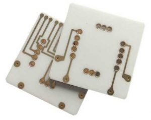
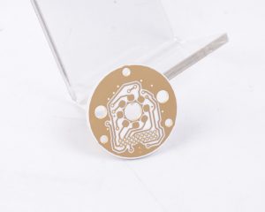
ceramic pcb prototype production is the controlled sample-building stage used to verify a ceramic circuit design before volume manufacturing. It helps engineers confirm substrate choice, copper pattern, thermal path, tolerances, assembly risk, and test requirements before committing to production tooling or a larger order.
For buyers and hardware teams, a ceramic PCB prototype is not just a small quantity of boards. It is a practical engineering checkpoint for high-power LEDs, power modules, sensors, RF designs, automotive electronics, medical devices, and other circuits where heat, dimensional stability, insulation, or reliability can decide whether the final product works.
What Is Ceramic PCB Prototype Production?
Ceramic PCB prototype production is the first manufacturing run of a ceramic circuit board design, usually built to validate the material, copper layout, process route, inspection plan, and assembly compatibility. The goal is to find manufacturability issues while the design can still be corrected without large production losses.
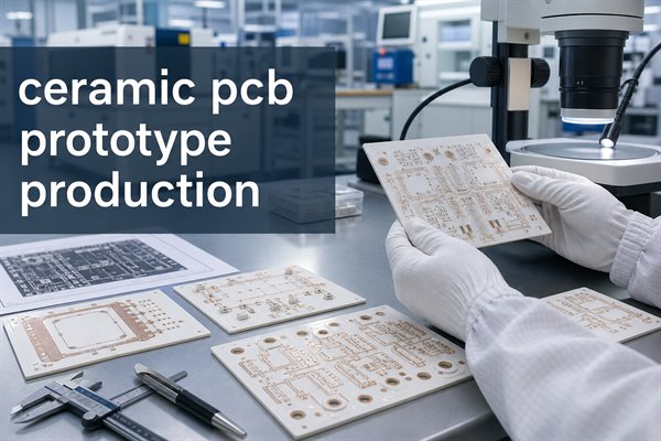
Unlike a standard FR4 prototype, a ceramic prototype depends heavily on substrate behavior, metallization method, firing or bonding process, conductor adhesion, surface flatness, and thermal expansion matching. A good prototype order should therefore answer both electrical and manufacturing questions, not only confirm that the Gerber files can be plotted.
For a new project, the prototype stage often confirms whether ceramic PCB technology is the right direction, or whether an alternative such as FR4 PCB or metal-core PCB is enough for the thermal and cost target.
Why Is Ceramic PCB Prototyping Different from FR4 PCB Prototyping?
Ceramic PCB prototyping is different because the substrate is rigid, hard, thermally conductive, and much less forgiving than glass-reinforced epoxy laminate. The process needs more attention to ceramic material selection, copper bonding, drilling or laser processing, dimensional tolerance, and thermal cycling behavior.
| Prototype factor | FR4 PCB prototype | Ceramic PCB prototype |
| Base material | Glass epoxy laminate | Al2O3, AlN, BeO alternatives, LTCC, HTCC, or other ceramic substrates |
| Main design concern | Signal routing, layer stack, cost, and standard fabrication limits | Thermal path, ceramic thickness, copper adhesion, CTE match, and process route |
| Mechanical behavior | Can flex slightly before fracture | Brittle and requires careful handling, panel design, and fixture planning |
| Prototype review focus | DFM, impedance, hole quality, solder mask, assembly fit | Metallization quality, substrate flatness, thermal design, edge quality, and inspection plan |
This difference affects the RFQ stage. A supplier should review not only the Gerber data, but also the ceramic material, copper thickness, board outline, via structure, tolerance needs, component heat load, and whether the prototype must support later mass production approval.
Which Ceramic PCB Material Should You Choose for a Prototype?
The best ceramic prototype material depends on thermal conductivity, insulation requirement, mechanical strength, cost target, and the final application environment. Al2O3 is commonly chosen for cost-effective ceramic prototypes, while AlN is often selected when higher thermal conductivity is required.
| Material or technology | Why it is used in prototypes | Typical review point |
| Al2O3 ceramic | Balanced cost, insulation, mechanical stability, and mature processing | Check whether thermal performance is enough for the heat load |
| AlN ceramic | Higher thermal conductivity for power and LED designs | Confirm cost, availability, and metallization compatibility |
| Thick film ceramic | Useful for printed conductor, resistor, and hybrid circuit structures | Review conductor geometry and fired pattern tolerance |
| Thin film ceramic | Used where fine lines, stable circuits, or precise patterns are needed | Confirm line width, adhesion, finish, and application fit |
| DPC, DCB, or related structures | Selected when copper thickness, thermal path, or power handling drives the design | Match the process route to copper thickness and reliability needs |
If the project is still early, ask the manufacturer to compare available ceramic options before confirming the prototype route. EBest Circuit supports ceramic PCB categories such as thick film ceramic PCB, thin film ceramic PCB, DPC ceramic PCB, and DCB ceramic PCB, so the prototype can be planned around the final production requirement instead of treated as an isolated sample.
What Is the Ceramic PCB Manufacturing Process?
The ceramic PCB manufacturing process usually starts with design review and material selection, then moves through substrate preparation, metallization, patterning, firing or bonding, surface finish, profiling, inspection, testing, and packing. The exact route depends on whether the project uses thick film, thin film, DPC, DCB, LTCC, HTCC, or another ceramic process.
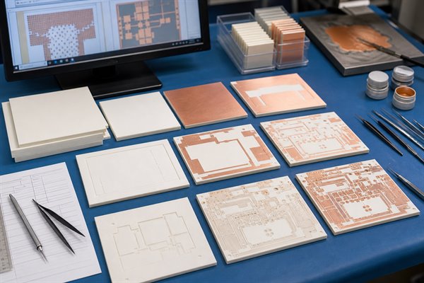
- Engineering review: Check Gerber files, drill data, board outline, copper thickness, substrate thickness, tolerances, and application requirements.
- Material preparation: Select Al2O3, AlN, or another ceramic substrate and confirm thickness, size, flatness, and handling needs.
- Metallization and patterning: Build the conductive layer using the selected process route, then define circuit features according to the design.
- Thermal or bonding process: Fire, sinter, plate, bond, or otherwise stabilize the conductor system depending on the technology.
- Finishing and profiling: Apply the required surface finish, cut the outline, and prepare the board for inspection or assembly.
- Inspection and test: Review dimensions, conductor quality, insulation, open/short status, surface quality, and packaging condition.
A prototype should be reviewed as a process sample. If the prototype later moves into production, the same data package, material choice, and inspection criteria should be stable enough to repeat.
How Do Thick Film, Thin Film, DPC and DCB Affect Prototype Production?
Different ceramic PCB process routes affect prototype cost, minimum features, copper thickness, thermal performance, and sample lead time. Choosing the process too late can force the engineering team to redesign pads, traces, vias, or thermal areas after the first prototype.
Thick film ceramic PCB is often used for hybrid circuits and printed conductor structures. It can be practical for prototypes where fired pastes, resistive elements, or ceramic-based circuit patterns are part of the design.
Thin film ceramic PCB is better suited for finer features and stable circuit requirements. It is often reviewed for sensor, microwave, medical, and precision electronic applications where conductor geometry matters.
DPC and DCB ceramic PCB routes are more closely tied to power electronics and heat transfer. For these prototypes, copper thickness, adhesion, thermal cycling, and substrate-to-copper reliability need early review.
What Files Are Needed for a Ceramic PCB Prototype Quote?
A ceramic PCB prototype quote is more accurate when the supplier receives a complete technical package, not just a screenshot or partial Gerber export. Missing tolerances, material notes, and assembly requirements can cause delays or a quote that does not match the real production risk.
- Gerber files and drill data
- Board outline drawing with critical dimensions
- Ceramic material preference, such as Al2O3 or AlN
- Substrate thickness and copper thickness requirement
- Surface finish requirement
- Panelization or single-piece delivery preference
- Quantity for prototype and expected production volume
- Assembly files if the prototype needs PCBA service
- Thermal, electrical, or reliability test requirements
- Application notes, especially for high-power, high-temperature, LED, sensor, or RF use
When a buyer provides both the prototype quantity and the expected mass production target, the manufacturer can recommend a route that avoids sample-only shortcuts that may not scale.
What Should You Check Before Moving from Prototype to Production?
Before moving from ceramic prototype to production, check whether the prototype truly validates the final design, process, material, and inspection standard. A board that passes a simple electrical test may still need thermal, mechanical, and assembly review before mass production.
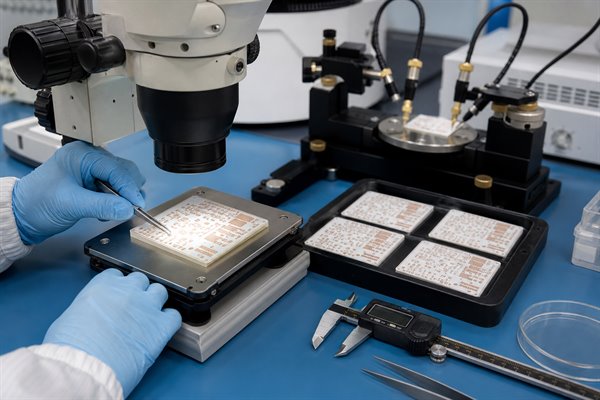
- Confirm the ceramic material and thickness match the final thermal design.
- Check conductor adhesion, line quality, edge quality, and surface finish.
- Review substrate flatness and dimensional tolerance against assembly needs.
- Test open/short status, insulation resistance, and critical electrical paths.
- Review solderability or bonding compatibility if components will be mounted.
- Record any design changes before approving the production file set.
- Ask whether the same process route will be used for the production batch.
The cleanest transition happens when the prototype report, customer feedback, corrected files, and final production requirements are all connected before the next purchase order.
What Problems Can Delay Ceramic PCB Prototype Production?
Ceramic PCB prototype production is often delayed by incomplete files, unclear material selection, unrealistic tolerances, process-route mismatch, missing assembly data, or late changes to the thermal design. These problems are easier to fix before production starts than after substrates and tooling have been prepared.
| Delay cause | Why it matters | How to prevent it |
| Unclear ceramic material | Al2O3, AlN, and other ceramics change cost and thermal behavior | Share heat load, application, and target cost before quoting |
| Missing tolerance drawing | Ceramic processing may need different tolerance planning than FR4 | Mark critical dimensions and non-critical dimensions separately |
| Wrong process route | Thick film, thin film, DPC, and DCB do not fit the same designs equally | Ask the supplier to review process fit before sample build |
| Late assembly requirement | Pad finish, flatness, and component heat transfer may need early planning | Send BOM, placement file, and assembly notes with the RFQ |
How to Choose a Ceramic PCB Prototype Manufacturer?
Choose a ceramic PCB prototype manufacturer by checking whether the supplier can review material selection, process route, DFM risk, inspection requirements, assembly needs, and future production scaling. Price matters, but the cheapest sample is not useful if the process cannot support the final product.
Good supplier questions include:
- Which ceramic materials and process routes are suitable for this design?
- Can the same route support prototype and mass production?
- What design features may increase cost or delay?
- Which tolerances should be relaxed if they are not functional?
- What tests are recommended for this application?
- Can assembly, inspection, and packaging be coordinated in one project flow?
EBest Circuit can support custom ceramic PCB projects from prototype review to sample production and later batch manufacturing. For projects that need assembled samples, prototype PCB fabrication can also be coordinated with PCBA review to reduce handoff risk.
FAQ
How much does a ceramic PCB prototype cost?
Ceramic PCB prototype cost depends on material, substrate thickness, copper thickness, process route, dimensions, tolerance level, quantity, surface finish, testing, and whether assembly is included. Al2O3 prototypes are often more cost-effective than higher thermal conductivity ceramic options, but the right choice should be based on the heat load and reliability target.
Can ceramic PCB prototypes be assembled?
Yes, ceramic PCB prototypes can be assembled when the pad finish, flatness, component package, soldering or bonding method, and thermal requirements are reviewed early. If assembly is needed, send the BOM, placement file, polarity notes, and any thermal interface requirements with the PCB quotation package.
Is Al2O3 or AlN better for ceramic PCB prototype production?
Al2O3 is often selected for balanced cost and mature processing, while AlN is chosen when higher thermal conductivity is required. The better option depends on the heat source, insulation requirement, mechanical design, available budget, and whether the prototype must represent a later production build.
Can one ceramic PCB prototype be used for mass production approval?
One prototype can support production approval only if it uses the same material, process route, design file set, tolerance standard, inspection method, and assembly assumptions planned for mass production. If the prototype used sample-only changes, a second verification run may be needed before release.
What tolerances matter most in ceramic PCB prototyping?
The most important tolerances are usually board outline, hole or slot position, substrate thickness, copper feature size, registration, flatness, and critical pad locations. The buyer should identify which dimensions affect assembly or function, because unnecessary tight tolerances can increase cost and delay without improving performance.
What is the difference between ceramic prototype and ceramic PCB prototype?
A ceramic prototype can refer to any trial part made from ceramic material, while a ceramic PCB prototype is a circuit board sample built on a ceramic substrate with conductive patterns for electronic use. For RFQ clarity, use ceramic PCB prototype when the part includes circuit fabrication requirements.
How Can EBest Circuit Support Ceramic PCB Prototype Production?
EBest Circuit supports ceramic PCB prototype production by helping buyers review materials, process route, manufacturability, inspection needs, and assembly requirements before moving into larger production. If you are developing a ceramic PCB for LED, power electronics, sensor, automotive, medical, or industrial electronics applications, send your files and requirements to the engineering team for a practical review and quotation at sales@bestpcbs.com.
You may also like

Tags: ceramic PCB, Ceramic PCB Production, ceramic PCB prototype production, pcb manufacturing, pcb prototype