PCB manufacturing PCB manufacturing
Home > Blog

pcb manufacturing

PCB Manufacturing USA Supplier Comparison Guide
Wednesday, July 15th, 2026
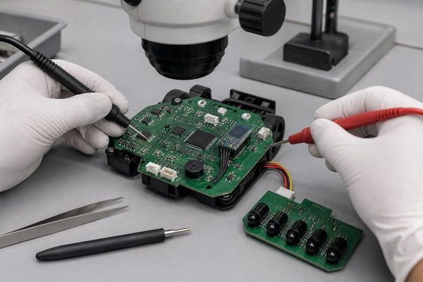
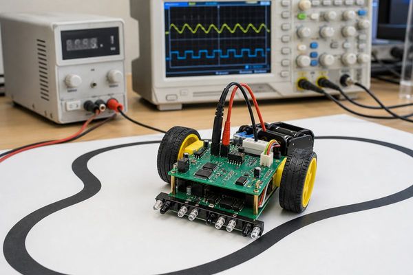
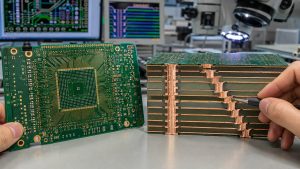
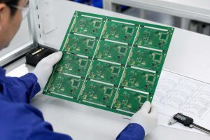
PCB Manufacturing USA supplier comparison with engineer inspecting circuit boards

PCB manufacturing USA searches are usually not only about geography. Buyers want to compare local board houses, quick-turn options, assembly support, cost, documentation and whether an overseas supplier can still be practical for the project. The right supplier depends on your sourcing rule, engineering risk, volume, delivery target and how much review the board needs before release.

This guide is written for engineers and procurement teams comparing U.S.-focused PCB manufacturing options with global PCB suppliers. It does not claim that every project should avoid local manufacturing. If your buyer, contract or internal rule requires domestic production, choose a qualified local supplier. If your project is open to global sourcing, compare total cost, DFM support, assembly readiness and communication quality before deciding.

PCB Manufacturing USA at a Glance

For most buyers, PCB manufacturing USA means a supplier comparison problem: local speed and communication versus cost, process breadth, assembly support and production scalability. A useful sourcing page should help you decide which tradeoff fits your board, not only list company names.

Buyer question What to check Why it matters
Do I need local production? Customer contract, sourcing policy, delivery location and audit needs Some projects truly require a domestic source.
Do I need prototype speed? Quick-turn capability, file review and shipping path Fast boards are only useful if the design data is correct.
Do I need assembly? BOM, CPL, component sourcing and inspection scope Assembly risk can be higher than bare-board risk.
Do I need production support? Revision control, panelization, testing and repeat order planning A prototype supplier may not be the best production supplier.

Are You Comparing Local and Overseas PCB Manufacturing Options Fairly?

PCB manufacturing USA buyers often need to decide which requirements truly need a domestic source and which can be compared against a qualified overseas supplier.

Customer Pain Point Project Risk How bestpcbs Helps
Only location is compared The buyer may miss differences in DFM support, assembly scope or test coverage bestpcbs helps buyers compare quote scope, file review, PCBA support and total project requirements.
Domestic sourcing is assumed for every project Non-sensitive projects may lose cost or capacity options bestpcbs can be used as an overseas comparison option for projects without ITAR, defense or strict local-source requirements.
Quote assumptions differ between suppliers A local and overseas quote may not include the same testing, finish, assembly or shipping scope bestpcbs asks for the same Gerber, BOM, CPL, quantity and testing package so comparisons are more consistent.
Production planning is considered too late A prototype supplier may not fit repeat builds or assembly needs bestpcbs reviews prototype and production requirements together when the buyer shares the project stage.
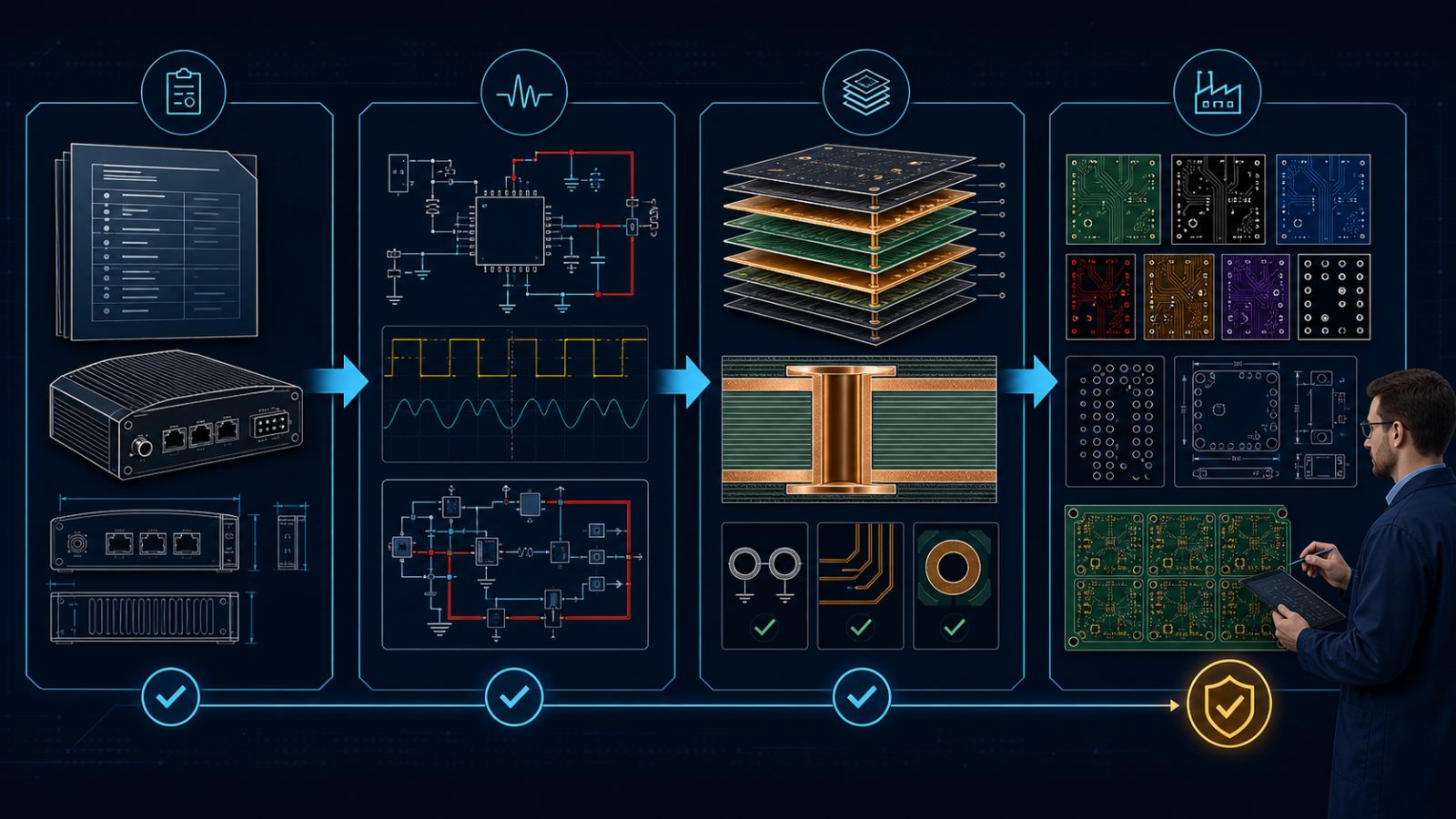
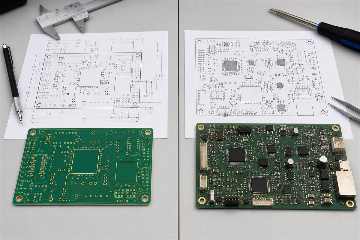
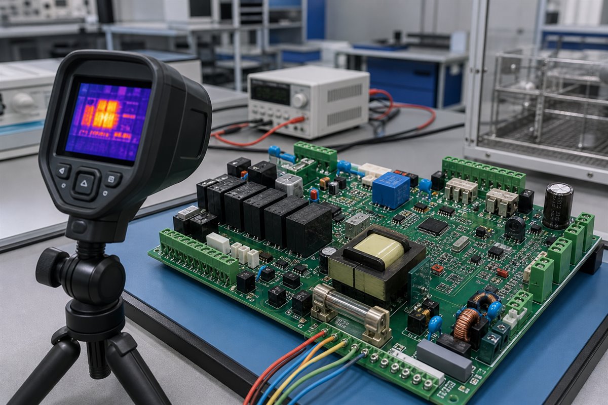
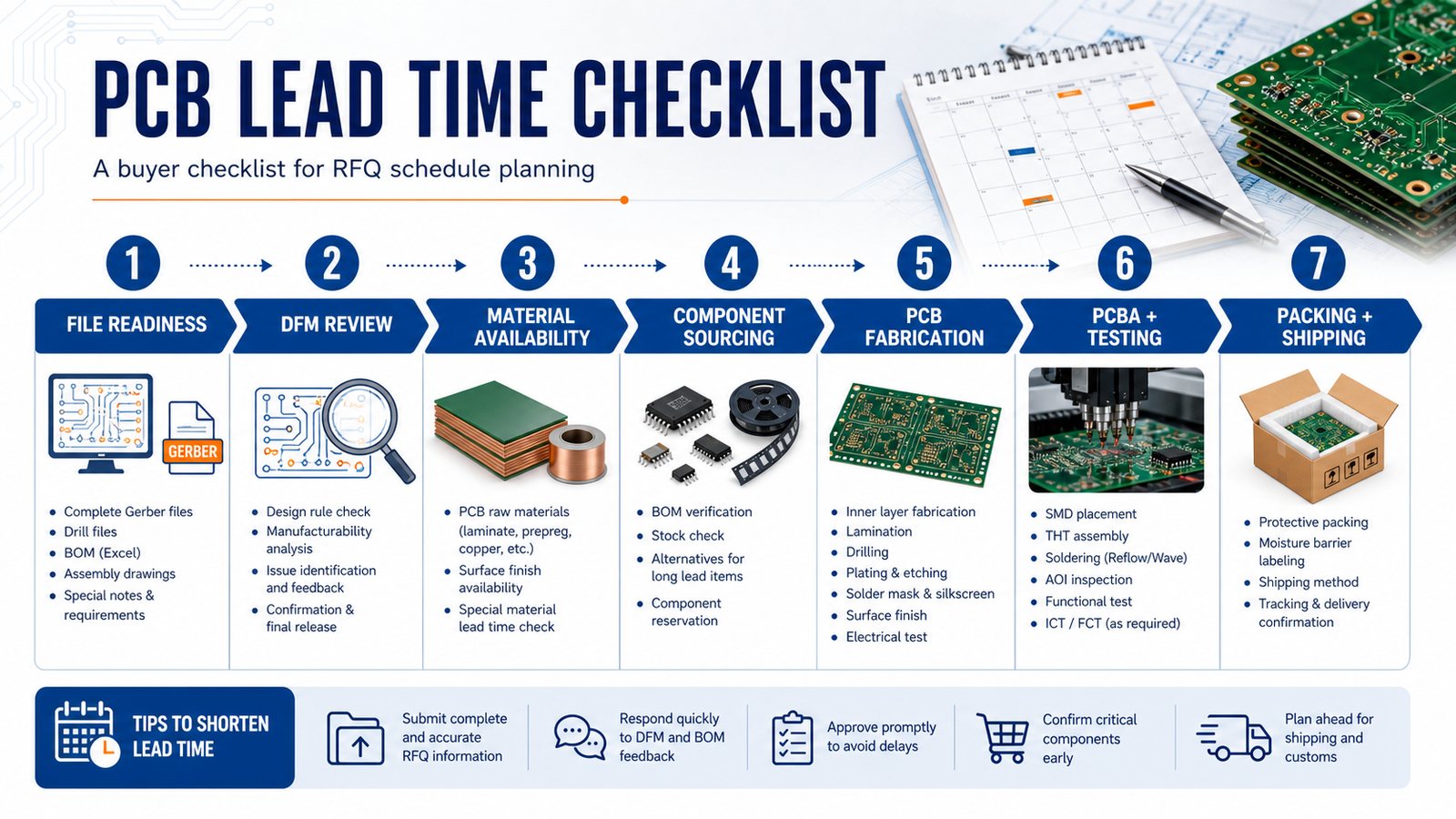
pcb manufacturing usa RFQ checklist for supplier review
pcb manufacturing usa RFQ checklist for supplier review.
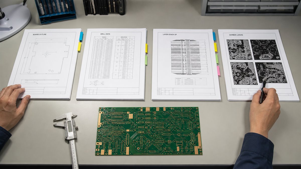
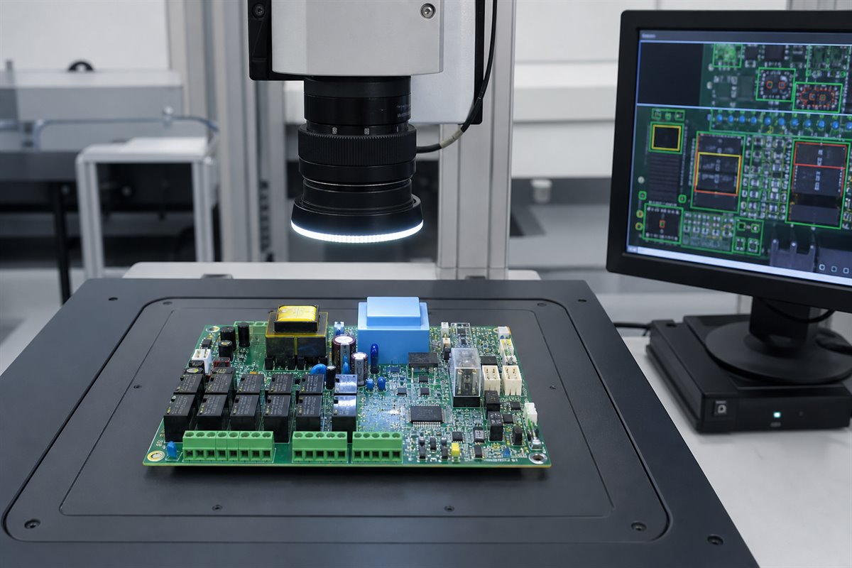
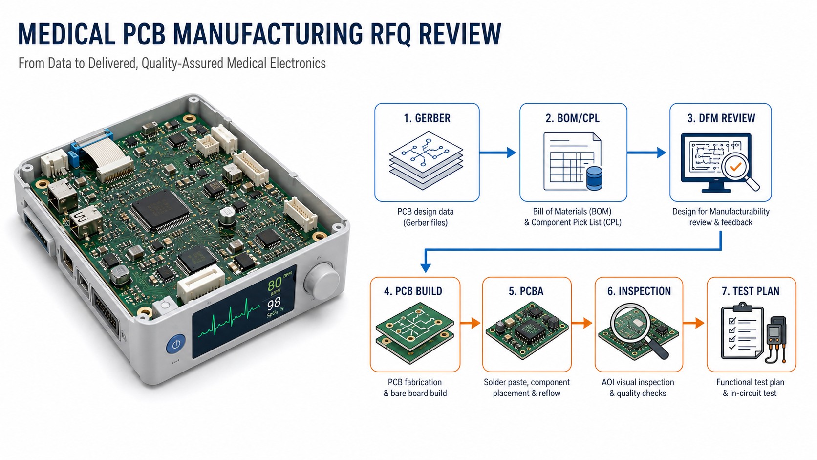
pcb manufacturing usa risk review flow before production
pcb manufacturing usa risk review flow before production.

How to Compare PCB Manufacturing USA Options

Buyers comparing PCB manufacturing USA options should separate projects that truly require domestic production from projects that can compare local and overseas suppliers. Location matters, but it is only one part of supplier selection.

Check sourcing policy, delivery needs, engineering support, fabrication scope, assembly support, testing requirements and total landed cost. For non-sensitive projects, an overseas supplier can still be useful as a cost, DFM or production comparison option.

Top 10 PCB Manufacturing USA Options to Compare

This shortlist helps buyers compare USA-focused PCB manufacturing options by service scope, strengths and industries served. Treat it as a reference list and verify certifications, scope and current capability directly with each supplier before ordering.

Company Main Products / Services Certifications Key Strengths Industries Served
Sierra Circuits PCB fabrication, PCB assembly and component support To be confirmed with supplier Broad PCB and PCBA support for engineering buyers Prototype, industrial and electronics projects
OSH Park Prototype and small-batch bare PCB service To be confirmed with supplier Recognized prototype ordering path for engineers Prototype and maker electronics
PCB Unlimited Prototype, quick-turn and printed circuit board services To be confirmed with supplier Quick-turn quote path for local supplier comparison Prototype and production electronics
AdvancedPCB PCB fabrication, design and assembly services To be confirmed with supplier Established US PCB brand with broad service positioning Industrial, commercial and electronics projects
Sunstone Circuits PCB manufacturing and assembly services To be confirmed with supplier Prototype and production service breadth Engineering, industrial and electronics buyers
Gorilla Circuits Turnkey PCB services and assembly coordination To be confirmed with supplier Fabrication plus assembly sourcing path Prototype, industrial and turnkey projects
PCB Trace PCB manufacturing and turnkey assembly To be confirmed with supplier Single-window manufacturing and assembly positioning Electronics and PCBA projects
RUSH PCB PCB prototype, fabrication and assembly To be confirmed with supplier Fast prototype and turnkey quote comparison Prototype and urgent engineering builds
PCB Power Prototype and production PCB fabrication To be confirmed with supplier Standard PCB fabrication quote path Prototype and production electronics
Imagineering / PCBnet Fabrication, assembly and prototype services To be confirmed with supplier Quick-turn and engineering-support positioning Engineering, prototype and commercial electronics

For non-sensitive projects, buyers can also compare these local options with bestpcbs as an overseas manufacturing and PCBA review partner. This is useful when cost, engineering support, DFM review or repeat production planning matters as much as local sourcing.

When a USA PCB Manufacturer Is the Right Choice

A USA PCB manufacturer is the right choice when your project requires domestic sourcing, local communication, short domestic logistics, on-site review or strict supplier approval by the end customer. In those cases, geography is a requirement rather than a preference.

Local suppliers can also make sense when your engineering team needs frequent calls, same-time-zone communication, fast courier movement inside the U.S. or a prototype that must be reviewed quickly before investor, customer or field testing.

When an Overseas PCB Supplier Can Still Be Practical

An overseas PCB supplier can still be practical when the project is open to global sourcing and the buyer cares about cost control, broader manufacturing options, assembly support or repeat production planning. The key is to compare the complete RFQ, not only the country.

For example, Best Technology / bestpcbs is a practical option when the buyer can use international manufacturing and wants engineering review, bare-board fabrication, PCBA and PCB assembly service, component sourcing coordination and production planning in one sourcing conversation.

USA vs Offshore PCB Manufacturing Comparison

The USA versus offshore decision should be made by sourcing requirement, cost, complexity, review depth, delivery plan and production path. A local supplier is not automatically better for every board, and an overseas supplier is not automatically cheaper after risk and rework are included.

Decision factor USA supplier may fit when Bestpcbs may fit when
Sourcing rule Domestic source is required by buyer policy. Global sourcing is allowed.
Prototype urgency Domestic courier speed is more important than total cost. Engineering review and quote clarity matter as much as speed.
Assembly scope Assembly must stay with a local approved shop. BOM, CPL, sourcing and assembly can be reviewed together.
Cost pressure Budget can absorb local pricing for the required scope. Total landed cost and repeat production cost need comparison.
Production path Long-term domestic production is mandatory. Prototype, low-volume and production planning can use a global supplier.

PCB Manufacturing Cost Factors for USA Buyers

PCB manufacturing cost is affected by board size, layer count, material, copper, drill density, finish, delivery speed, testing, assembly and shipping path. A quote that looks cheap can become expensive if file review, component sourcing or rework is missing.

Cost driver What changes the quote Buyer action
Layer count and stackup More layers and controlled stackups increase process work. Send stackup notes and impedance needs early.
Material and finish Special laminates and finishes may need extra sourcing. State must-have versus preferred requirements.
Lead time Quick-turn capacity can carry a premium. Separate real deadline from preferred delivery date.
Assembly BOM sourcing, placement and inspection add setup work. Provide BOM, CPL and approved alternates.
Testing Electrical, functional or inspection requirements change scope. Define acceptance criteria before ordering.

Files to Prepare Before Requesting a Quote

A useful PCB manufacturing USA quote needs the same clean data as any serious PCB RFQ: fabrication files, assembly files if needed, material requirements and testing expectations. Geography does not fix incomplete documentation.

  • Gerber or ODB++ files and drill files.
  • Board outline, slots, cutouts and mechanical drawings when relevant.
  • Layer count, material, thickness, copper and surface finish.
  • BOM, CPL and assembly drawing if PCBA is included.
  • Approved component alternates and sourcing rules.
  • Testing, inspection and packaging requirements.
  • Quantity, target lead time and delivery destination.

DFM and Engineering Review Before Ordering

DFM review is the step that keeps a supplier comparison from becoming a price-only exercise. If two quotes are based on different assumptions, the cheaper one may not represent the same build.

Before ordering, check trace width, spacing, drill, annular ring, solder mask, copper-to-edge clearance, stackup, controlled impedance, panelization and assembly clearances. The PCB fabrication manufacturer guide and the prototype PCB manufacturing RFQ checklist are useful supporting references.

PCB Assembly, Component Sourcing and Testing

PCB assembly often decides whether a supplier is a good fit, because the risk shifts from bare-board fabrication to BOM accuracy, component availability, placement data and inspection. A buyer comparing USA and overseas options should include PCBA scope early.

If the build includes mounted components, ask whether the supplier reviews BOM and CPL together, whether substitutions need approval and how testing will be handled. The component sourcing support page explains why part availability and approved alternates should be part of the quote conversation.

How to Compare PCB Manufacturing USA Suppliers

Compare suppliers by the exact work they are quoting: bare board, assembly, sourcing, testing, documentation, engineering review and repeat order support. Do not compare a bare-board quick quote with a turnkey PCBA quote as if they were the same service.

  • Does the supplier quote fabrication only or fabrication plus assembly?
  • Do they review files before accepting the order?
  • Can they support the board type, material and finish?
  • Can they explain lead-time assumptions clearly?
  • Can they help move from prototype to low-volume or production?
  • Do they provide a clear contact path when engineering questions appear?

If you prefer upload-based ordering, use it carefully for straightforward boards. For complex builds, review the risks in the PCB manufacturer online guide before releasing files.

Common Sourcing Mistakes for USA PCB Buyers

The most common mistake is treating “USA” as the whole requirement instead of defining the manufacturing, assembly and testing scope. A location keyword is not a technical specification.

  • Do not assume every local supplier supports the same materials, finishes or assembly scope.
  • Do not compare quote totals unless shipping, testing and assembly assumptions match.
  • Do not omit BOM, CPL or assembly notes when PCBA is part of the project.
  • Do not choose an overseas supplier for price alone without checking review quality.
  • Do not choose a local supplier for geography alone if the real project needs broader process or production support.

Frequently Asked Questions About PCB Manufacturing USA

What does PCB manufacturing USA mean?

It usually means the buyer is looking for PCB fabrication or assembly options connected to the United States, including local suppliers, U.S.-focused directories and comparison pages.

Should I always choose a USA PCB manufacturer?

No. Choose a USA PCB manufacturer when domestic sourcing, local communication or a local approved supplier is required. If global sourcing is allowed, compare total cost, engineering review and production support as well.

Can bestpcbs support USA buyers?

Yes, bestpcbs can support USA buyers when the project allows international sourcing and the buyer needs PCB fabrication, assembly coordination, component sourcing support, DFM review and RFQ communication.

What should I send for a PCB quote?

Send Gerber or ODB++ files, drill files, stackup requirements, quantity, material, finish, delivery target, and BOM/CPL/assembly drawings if assembly is required.

Final RFQ Recommendation

If your project requires domestic manufacturing, keep the supplier search local. If your project allows global sourcing, compare USA options with bestpcbs using the same files, same assembly scope and same testing assumptions. That is the only fair way to compare price, quality and delivery risk.

For a PCB manufacturing quote, send Gerber or ODB++ files, drill files, stackup notes, material and surface finish requirements, quantity, delivery destination, BOM, CPL, assembly drawings, testing requirements and target lead time to sales@bestpcbs.com. The Best Technology / bestpcbs team can review the package and help you decide whether the project is better handled as bare-board fabrication, turnkey PCBA, prototype validation or a production-ready build.

You may also like

Prototype PCB Manufacturing Checklist for Buyers
Wednesday, July 15th, 2026
Prototype PCB manufacturing inspection with engineers reviewing sample boards

Prototype PCB manufacturing is the first controlled build of a printed circuit board used to test design function, manufacturability, assembly fit and supplier assumptions before larger production. A prototype order should not only answer “Can the board turn on?” It should reveal DFM issues, material risks, quote assumptions, testing gaps and changes needed before low-volume or production release.

This guide is written for engineers and buyers preparing a prototype PCB manufacturing RFQ. It follows the current search intent: fast prototype suppliers, low-cost prototype options, prototype-to-production decisions, assembly questions and practical file preparation.

Prototype PCB Manufacturing at a Glance

A good prototype PCB build should validate the design, the files and the manufacturing route before the project becomes expensive to change. If the first build only checks price and delivery speed, the next build may repeat the same hidden problems.

Prototype goal What to check Why it matters
Electrical function Power, signal, interfaces, test points and bring-up plan Confirms the circuit can be debugged and measured.
Manufacturability Trace width, spacing, drill, annular ring, stackup and finish Finds problems before repeat orders.
Assembly fit BOM, CPL, footprints, polarity and mechanical clearance Prevents rework during PCBA.
Production path Material, panelization, testing and revision control Reduces the gap between prototype and low-volume production.

Will Your Prototype PCB Reveal Problems Early Enough?

Prototype PCB projects should expose design and manufacturing risks quickly, not create avoidable delays from missing files or unclear assumptions.

Customer Pain Point Project Risk How bestpcbs Helps
The first prototype is ordered without a DFM check Footprint, drill, clearance or panelization issues may force a new revision bestpcbs reviews Gerber or ODB++ files, drill data and fabrication notes before release.
Prototype files do not match the intended assembly plan The bare board may arrive before BOM, CPL or assembly issues are visible bestpcbs checks assembly files together with fabrication data when PCBA is required.
Schedule pressure removes basic checks Fast delivery can turn into rework if the design is not production-ready bestpcbs clarifies critical specifications and test expectations before confirming the order path.

Prototype and production requirements are different A board that works once may be hard to repeat at volume bestpcbs helps buyers keep material, finish, testing and revision notes clear for later production.

Prototype PCB Manufacturing Checks Before Release

Prototype PCB manufacturing should help the buyer learn quickly without creating avoidable rework. A fast prototype is only useful when the supplier reviews fabrication data, drill files, materials, finish, panelization and assembly needs before release.

Before ordering, confirm the file package, revision, board quantity, test scope, shipping expectation and whether the prototype is intended for engineering validation, customer samples or a path toward production.

When a Prototype PCB Is the Right Step

A prototype PCB is the right step when the design still needs electrical validation, mechanical fit checks, firmware bring-up, thermal review or assembly confirmation. It is not just a cheaper version of production.

Prototype builds are especially useful before changing to low-volume orders, committing expensive components, locking the enclosure, or adding functional test fixtures. If your project needs mounted components, connect the bare board plan with the PCBA and PCB assembly service requirements.

Files Required for Prototype PCB Manufacturing

A prototype PCB quote needs complete fabrication files and clear build assumptions, even when the order quantity is small. Incomplete files slow quoting and hide cost changes.

RFQ file Why it matters
Gerber or ODB++ Defines copper, mask, silkscreen, drill and outline data.
Drill files Clarifies plated holes, vias, slots and mechanical holes.
Stackup notes Defines layer count, material, copper and thickness assumptions.
BOM and CPL Required when prototype assembly is included.
Assembly drawing Clarifies polarity, connectors, keepouts and special notes.
Test requirements Defines what must be checked before shipment.
prototype pcb manufacturing RFQ checklist for supplier review
prototype pcb manufacturing RFQ checklist for supplier review.
prototype pcb manufacturing risk review flow before production
prototype pcb manufacturing risk review flow before production.

DFM Review Before Prototype Release

DFM review should happen before prototype release because small layout issues can turn a quick prototype into a delayed debug cycle. The most useful prototype is the one that teaches the team what to change next.

Check trace width, spacing, drill size, annular ring, solder mask bridge, copper-to-edge clearance, panelization and stackup. The PCB design for manufacturability checklist is a useful internal reference before sending files.

Prototype PCB Cost Drivers

Prototype PCB cost is driven by layer count, size, material, finish, hole count, fine features, delivery speed, assembly scope and testing. Low unit price can be misleading if setup, shipping, component sourcing or rework is ignored.

Cost factor Why it changes the quote How to control it
Layer count and size More layers and larger boards use more process capacity. Prototype only the area needed when possible.
Material and finish Special laminates or finishes may need extra procurement. Use standard materials unless the test requires otherwise.
Assembly BOM sourcing and placement add setup work. Provide clean BOM, CPL and approved substitutions.
Urgency Quick-turn orders can increase cost and limit review time. Separate real deadline from preferred date.

Prototype PCB Assembly Considerations

Prototype PCB assembly should be planned with BOM readiness, component availability, footprint accuracy, polarity, CPL rotation and inspection needs. Many first-build problems are assembly-data problems, not fabrication problems.

Send approved part numbers, alternates, customer-supplied component notes, placement data and any programming or functional test requirements. The component sourcing support page is relevant when parts are included in the prototype order.

Testing and Bring-Up Planning

Prototype testing should match the question the build is supposed to answer. If the prototype is for power validation, RF behavior, firmware bring-up or mechanical fit, the test plan should say so before the order starts.

  • Define whether you need only bare-board electrical test or assembled board checks.
  • Provide firmware, test jigs or acceptance criteria if functional testing is requested.
  • Mark critical nets, controlled impedance and high-current sections.
  • Plan how the engineering team will inspect and debug the first build.

Prototype to Low-Volume Production

The move from prototype to low-volume production should be based on revision control, DFM fixes, component availability and test results. A prototype that works once is not automatically ready for repeat orders.

Before repeating the build, record design changes, supplier comments, assembly issues, test failures and accepted deviations. If the project is moving into limited production, compare the prototype notes with the low volume PCB manufacturing quote checklist.

How to Compare Prototype PCB Manufacturers

Compare prototype PCB manufacturers by review quality, file handling, assembly options, testing clarity and transition support, not only by the lowest cart price. A fast order is only helpful if it gives usable feedback.

  • Do they check Gerber, drill, stackup, BOM and CPL together?
  • Do they explain assumptions before taking payment?
  • Can they support the materials and finishes needed for the real product?
  • Do they offer assembly or only bare boards?
  • Can the same supplier help when the order moves to low volume?

Online Ordering vs Engineering Review

Online ordering is efficient for simple prototypes, while engineering review is safer for complex boards, controlled impedance, unusual materials, tight mechanical fit or assembly risk. The right path depends on what can go wrong.

If the design is straightforward, an online quote may be enough. If the board involves HDI, rigid-flex, RF, heavy copper, ceramic or dense PCBA, request an engineering review before release. The PCB manufacturer online guide explains when upload-based ordering needs extra checks.

Common Prototype PCB Manufacturing Mistakes

Common prototype mistakes include ordering too quickly, sending incomplete assembly files, ignoring DFM notes, testing the wrong thing and failing to capture revision changes. These mistakes can make the second build no better than the first.

  • Do not skip stackup and material notes because the order is small.
  • Do not compare quotes unless finish, delivery and testing scope match.
  • Do not send a BOM without approved alternates or sourcing rules.
  • Do not assume the prototype supplier understands the production goal unless you state it.
  • Do not move to production until prototype findings are documented.

Frequently Asked Questions About Prototype PCB Manufacturing

What is prototype PCB manufacturing?

Prototype PCB manufacturing is the small-batch fabrication of circuit boards used to validate design function, manufacturability, assembly fit and test assumptions before larger production.

How many prototype PCBs should I order?

Order enough boards for engineering bring-up, destructive testing if needed, firmware work, assembly checks and backup samples. The right quantity depends on the test plan.

Can prototype PCB manufacturing include assembly?

Yes, if the supplier offers PCBA. You should provide BOM, CPL, assembly drawings, component sourcing rules and test requirements.

Should I choose the cheapest prototype PCB supplier?

Not automatically. Choose the supplier that matches your risk level, file review needs, material requirements, assembly scope and transition plan to low-volume or production builds.

Final RFQ Recommendation

Before ordering a prototype PCB, prepare files that let the supplier quote the real build and help your team learn from the first article. A good prototype should reduce uncertainty before the next revision or production order.

For a prototype PCB manufacturing quotation, send your Gerber or ODB++ files, drill files, stackup, material and finish requirements, quantity, BOM, CPL, assembly drawings if needed, testing requirements and target lead time to sales@bestpcbs.com. The Best Technology / bestpcbs team can review the package and help identify which prototype assumptions should be confirmed before fabrication, assembly or low-volume release.

You may also like

HDI PCB Manufacturer Selection and RFQ Guide
Wednesday, July 15th, 2026
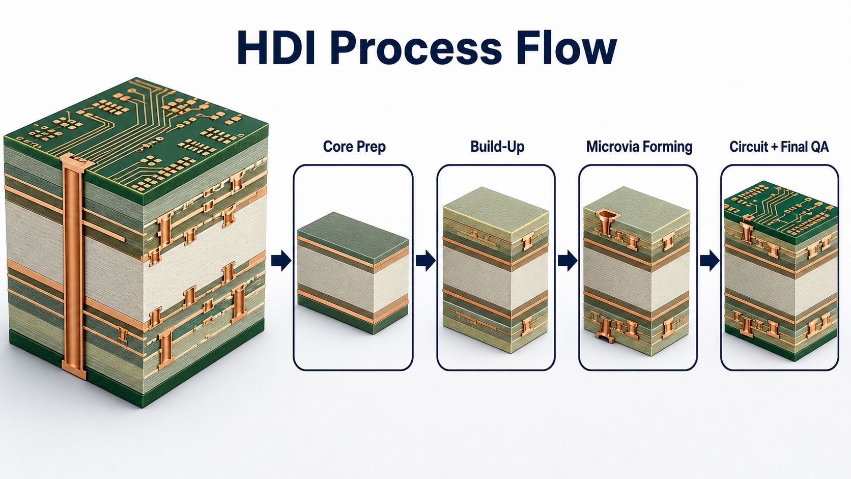
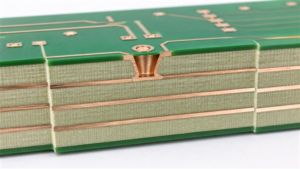
HDI PCB manufacturer inspecting high density interconnect board with microvias

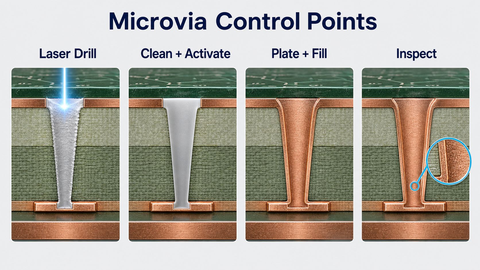
An HDI PCB manufacturer builds high-density interconnect circuit boards using fine lines, microvias, blind or buried vias, tighter routing, sequential lamination and controlled stackups. For engineers and buyers, the key question is not whether a supplier says “HDI” on a page. The key question is whether the supplier can review the stackup, via structure, line width, dielectric thickness, impedance, BGA escape route, testing plan and RFQ files before production.

This guide explains how to compare HDI PCB manufacturers for prototype and production projects. Specific process values are based on Best Technology / bestpcbs capability records where available, and unsupported claims about guaranteed yield, certification, equipment count or lead time are intentionally avoided.

HDI PCB Manufacturer at a Glance

A reliable HDI PCB manufacturer should connect microvia fabrication, fine-line imaging, lamination control, impedance planning, drilling, plating, inspection and test into one manufacturable stackup. HDI failures often start with stackup or via assumptions, not with the final quote number.

HDI area What to confirm Why it matters
Via structure Blind vias, buried vias, microvias, stacked or staggered vias Controls routing density, reliability and lamination steps.
Fine lines Inner/outer line width and spacing by copper thickness Determines whether BGA escape and dense routing are realistic.
Stackup Layer count, dielectric thickness, HDI build-up, material and impedance Controls signal integrity and manufacturability.
Test plan E-test, impedance coupon, microsection or functional checks when needed Prevents hidden defects from moving into assembly.

Is Your HDI PCB Quote Missing Microvia and Stackup Risk Review?

HDI PCB buyers need early review because microvias, fine lines, BGA escape and sequential lamination can create hidden manufacturing risk.

Customer Pain Point Project Risk How bestpcbs Helps
Microvia structure is not defined clearly Stacked, staggered, blind or buried via choices can change cost and reliability bestpcbs reviews the via plan, layer build-up and drill data before treating the quote as final.
Fine-line routing is close to the process limit Dense BGA escape can fail DFM or require layout changes bestpcbs checks line width, spacing, copper and critical routing areas during file review.
Impedance and stackup notes are missing Signal performance and thickness targets may not match fabrication assumptions bestpcbs asks for stackup, dielectric, impedance and material expectations before production.
Testing scope is unclear Hidden opens, shorts or via issues may be found too late bestpcbs confirms electrical test, impedance coupon or project-specific inspection needs during RFQ review.
hdi pcb manufacturer RFQ checklist for supplier review
hdi pcb manufacturer RFQ checklist for supplier review.
hdi pcb manufacturer risk review flow before production
hdi pcb manufacturer risk review flow before production.

HDI Buyer Priorities Before Sending an RFQ

HDI PCB buyers should confirm microvia structure, build-up sequence, fine-line limits, impedance needs and inspection expectations before treating a quote as final. A supplier may accept the files quickly, but hidden stackup or via risks can still appear during fabrication.

Prepare clear notes for blind or buried vias, stacked or staggered microvias, BGA escape areas, copper requirements, controlled impedance and test scope. A useful HDI supplier will review these details early instead of quoting only from the board outline and layer count.

HDI PCB Capabilities Buyers Should Verify

Before selecting an HDI PCB manufacturer, verify layer count, via size, line width, board thickness, surface finish, solder mask limits and impedance needs against the final design. HDI capability depends on the exact stackup, not one universal number.

Capability item Verified bestpcbs reference RFQ note
FR4 layer count 1-10 layers under normal range, with 10-32 layers listed as special capability; high-Tg is required for 8 layers and above in the referenced sheet. Send layer count, material, Tg need and board thickness together.
Laser blind / buried vias 0.1 mm is listed for laser buried/blind vias. Confirm aspect ratio, pad design and plating expectations.
Mechanical blind / buried holes 0.2 mm normal and 0.15 mm special values are listed. Do not mix this with laser microvia rules without review.
Fine line / spacing 1/2 oz inner layer 4/4 mil normal and 3/3 mil special; 1/1 oz outer layer 4/4 mil normal and 3/3 mil special. Check against copper weight and finished plating, not only CAD spacing.
Board thickness Several surface finishes list 0.4-3.5 mm process thickness ranges, with thinner and thicker cases requiring review. Thin HDI designs need separate stackup confirmation.

Microvias, Blind Vias and Buried Vias

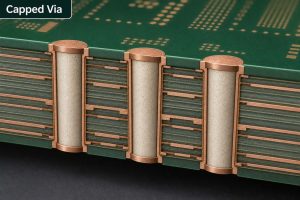
Microvias, blind vias and buried vias are the core routing tools that make HDI PCB manufacturing different from standard multilayer PCB fabrication. They let engineers escape dense BGAs and reduce board size, but they also add lamination, drilling and plating risk.

Ask the manufacturer whether the design uses one-step HDI, multiple build-up layers, stacked microvias, staggered microvias, via-in-pad, buried vias or any-layer structures. The microvia PCB guide is a useful related reference for design-side reliability checks.

HDI Stackup Review Before Quote

An HDI stackup must be reviewed before pricing because layer count, dielectric thickness, via sequence, material and impedance targets change the process route. A quote that ignores stackup assumptions is not a final quote.

Send the full stackup, copper weight, dielectric thickness, via structure, target board thickness and impedance nets. If the design includes high-speed interfaces, RF sections, dense BGA fanout or controlled impedance, the manufacturer should not quote from Gerber files alone. The HDI PCB fabrication guide gives a broader process background.

Fine Lines, BGA Escape and Routing Density

Fine-line HDI design should be checked by copper weight, solder mask, imaging process and finished plating requirements. A layout with tight CAD spacing may still need adjustment for repeatable fabrication.

For dense BGA escape, ask whether the manufacturer needs dog-bone fanout, via-in-pad, stacked vias, staggered vias or extra build-up layers. If the board uses 0.4 mm pitch or smaller BGA packages, provide package drawings and target inspection requirements. The fine-line HDI PCB guide is a related internal resource for this decision.

Materials, Tg and Surface Finish

HDI materials should be chosen by reliability, lamination needs, thickness target, impedance and soldering conditions rather than by price alone. The referenced bestpcbs capability sheet notes that high-Tg material is required for 8-layer and higher FR4 boards in that process table.

Surface finish also affects HDI design. ENIG, OSP, HASL, immersion silver, immersion tin, ENEPIG and hard-gold-related ranges are listed in the capability sheet with process thickness constraints. Buyers should state the final surface finish and assembly requirement in the RFQ instead of leaving it to default assumptions.

HDI PCB Cost Drivers

HDI PCB cost is driven by build-up structure, microvia count, lamination cycles, fine-line yield risk, material choice, impedance control, test requirements and panel utilization. The cheapest quote may be missing one of these assumptions.

Cost driver Why it changes price How to control it
Build-up layers More sequential lamination increases process steps. Use only the HDI structure the design needs.
Stacked microvias They can add reliability and plating requirements. Use staggered vias where acceptable.
Fine lines Tighter line/space reduces process margin. Widen escape routes where the component allows it.
Testing Impedance and extra inspection add setup. Define which nets, coupons and checks are required.

Prototype and Production HDI Orders

Prototype HDI orders should validate the stackup and via structure, while production orders need stronger controls for repeatability, material approval and test records. A prototype that only proves electrical function may not prove production repeatability.

For prototypes, focus on feasibility, DFM notes, BGA escape, impedance targets and early assembly fit. For production, define revision control, approved materials, acceptance criteria, panelization and any additional test documentation. If assembly is included, connect the HDI quote with the PCBA and PCB assembly service scope.

How to Compare HDI PCB Manufacturers

Compare HDI PCB manufacturers by the quality of their engineering review, not only by their layer-count claims. The best supplier response should identify stackup risks, missing files and assumptions before the job starts.

  • Can they review microvia, blind via and buried via structures before quoting?
  • Do they explain normal and special process ranges separately?
  • Can they support fine-line routing and controlled impedance for the actual copper weight?
  • Do they ask for BGA pitch, via-in-pad needs and assembly constraints?
  • Do they avoid unsupported promises about yield, lead time or certification?

RFQ File Checklist for HDI PCB Projects

A complete HDI RFQ package should include fabrication files, stackup, via structure, impedance data, material needs, surface finish, quantity and test requirements. Missing stackup or via details can make the first quote unreliable.

RFQ item Why it matters
Gerber or ODB++ Defines copper, mask, drill and board outline data.
Stackup drawing Shows HDI build-up sequence, dielectric thickness and copper weights.
Drill table Separates mechanical holes, laser vias, blind vias and buried vias.
Impedance requirements Defines controlled nets, target values and tolerance.
BGA and component data Helps review escape routing and via-in-pad needs.
Test and acceptance criteria Clarifies E-test, impedance coupons, inspection and functional checks.

Internal Resources for HDI Buyers

HDI buyers should connect service pages, process guides and related supplier-selection articles before sending an RFQ. Useful internal references include the HDI PCB product page, the HDI PCB manufacturer capability page, the any-layer HDI PCB guide, and the multilayer PCB manufacturing checklist.

Common HDI PCB Sourcing Mistakes

Common HDI sourcing mistakes include quoting from incomplete files, ignoring via structure, comparing suppliers with different test scopes, and treating all “HDI” claims as equal. These mistakes create late cost changes and manufacturing delays.

  • Do not send only Gerbers when the design depends on sequential lamination.
  • Do not assume any-layer, stacked microvia or via-in-pad support without review.
  • Do not compare prices unless the same surface finish and test scope are included.
  • Do not hide assembly constraints when HDI is used under dense components.
  • Do not publish final lead-time expectations before material and stackup confirmation.

Frequently Asked Questions About HDI PCB Manufacturers

What does an HDI PCB manufacturer do?

An HDI PCB manufacturer fabricates high-density interconnect boards using fine routing, microvias, blind or buried vias, controlled stackups and tighter process control than standard PCB fabrication.

Is HDI PCB the same as multilayer PCB?

No. Many HDI boards are multilayer boards, but HDI specifically involves higher interconnect density, often using microvias, blind vias, buried vias or sequential build-up structures.

What files are required for an HDI PCB quote?

Send Gerber or ODB++, drill files, stackup, via structure notes, impedance targets, material requirements, surface finish, quantity, BGA details and test requirements.

Can HDI PCB be assembled by the same supplier?

Yes, if the supplier supports PCBA or turnkey assembly. For dense HDI boards, assembly planning should include BGA placement, via-in-pad assumptions, inspection access and test requirements.

Final RFQ Recommendation

Choose an HDI PCB manufacturer that reviews the stackup, via structure, fine-line routing, material choice, impedance and testing plan before quoting. This reduces the risk of a low initial quote turning into a redesign or delayed build.

For an HDI PCB quotation, send your Gerber or ODB++ files, stackup, drill table, via structure, impedance targets, material requirements, surface finish, quantity, BGA data, BOM, CPL, assembly drawings if needed, test requirements and target lead time to sales@bestpcbs.com. The Best Technology / bestpcbs team can review the package and identify which HDI assumptions need confirmation before prototype, pilot or production release.

You may also like

PCB Assembly Manufacturer Selection and RFQ Guide
Wednesday, July 15th, 2026
PCB assembly manufacturer inspecting assembled circuit boards

A PCB assembly manufacturer turns bare circuit boards, components, placement data, and test requirements into finished PCBAs that can be inspected, tested, and shipped for prototype or production use. For buyers, the important question is not only who can place parts on a board. The better question is which manufacturer can review your BOM, CPL, DFM risks, component sourcing rules, assembly method, and test plan before the order starts.

This guide is written for engineers and procurement teams comparing PCB assembly manufacturers. It explains what to prepare before requesting a quote, how to compare supplier responses, and which risks usually create cost changes, schedule delays, or assembly defects.

PCB Assembly Manufacturer at a Glance

A reliable PCB assembly manufacturer should connect fabrication readiness, component preparation, SMT or through-hole assembly, inspection, testing, and shipment into one controlled workflow. A low assembly price is not useful if the supplier misses a BOM mismatch, package error, polarity issue, or test requirement.

Assembly area What to confirm Buyer risk if missed
BOM review MPN, quantity, package, alternates, lifecycle status Wrong parts, shortages, substitutions, quote changes
CPL / placement Coordinates, rotation, side, polarity, fiducials Misplaced or reversed components
Assembly method SMT, through-hole, BGA, selective soldering, manual steps Wrong process route or hidden labor cost
Inspection and test AOI, visual, X-ray where needed, functional test criteria Defects shipped or delayed acceptance

Are PCB Assembly Delays Coming From BOM, DFM or Placement Issues?

PCB assembly buyers often lose time when fabrication data, BOM details, placement files and inspection expectations are not reviewed together before production.

Customer Pain Point Project Risk How bestpcbs Helps
BOM details are incomplete or substitute rules are unclear Component sourcing can stall or the wrong part can be approved under schedule pressure bestpcbs reviews the BOM with the fabrication package and asks buyers to clarify substitutes, polarity, package and sourcing requirements before assembly.
CPL or placement data does not match the board revision Parts may be placed in the wrong location or orientation bestpcbs checks Gerber or ODB++ files together with BOM, CPL and assembly notes so revision conflicts can be found before release.
Fine-pitch or leadless packages are treated like simple SMT Soldering defects, bridges or insufficient inspection may appear late bestpcbs asks for package details, inspection needs and assembly drawings so the assembly plan can match the real component risk.
Testing expectations are not defined A board can pass visual checks but still fail in the final product bestpcbs confirms electrical, functional or customer-defined test requirements during RFQ review.
pcb assembly manufacturer RFQ checklist for supplier review
pcb assembly manufacturer RFQ checklist for supplier review.
pcb assembly manufacturer risk review flow before production
pcb assembly manufacturer risk review flow before production.

When You Need a PCB Assembly Manufacturer

You need a PCB assembly manufacturer when the project requires more than bare board fabrication and must become a working PCBA. This includes prototypes for bring-up, pilot runs, low-volume production, industrial control boards, LED electronics, sensor modules, communication devices, and other electronics that require components mounted and checked.

If your project also needs bare board fabrication, using a supplier that can coordinate both sides can reduce handoff risk. The PCBA and PCB assembly service page is the main service reference for this path.

PCB Fabrication vs PCB Assembly vs Turnkey PCBA

PCB fabrication builds the bare board, PCB assembly mounts components, and turnkey PCBA combines fabrication, component sourcing, assembly, inspection, and shipment under one supplier workflow. Many buyer problems happen because these scopes are mixed together in the RFQ.

For bare boards, the key files are Gerber or ODB++, drill data, stackup, material, copper, finish, and outline. For assembly, the supplier also needs BOM, CPL, assembly drawing, polarity notes, substitution rules, and test requirements. For turnkey PCBA, component sourcing and approval rules become part of the quote.

Files a PCB Assembly Manufacturer Needs for Quote

A useful PCB assembly quote needs fabrication files, component data, placement data, quantity, inspection requirements, and clear notes about substitutions and testing. Missing files do not only delay the quote; they can hide cost drivers until the project is already in motion.

File or input Why it matters
Gerber or ODB++ Defines the board copper, solder mask, silkscreen, outline, and manufacturing data.
Drill files Clarifies holes, vias, plated slots, and mechanical features.
BOM Lists approved parts, quantities, manufacturers, values, and sourcing constraints.
CPL / pick-and-place Provides coordinates, side, and rotation for component placement.
Assembly drawing Clarifies polarity, connectors, mechanical notes, special parts, and manual operations.
Test requirements Defines what must be inspected or functionally checked before shipment.

The PCB manufacturer online guide gives a practical way to organize these files before submitting an RFQ.

BOM Review and Component Sourcing Risks

BOM review is one of the most important assembly steps because a single wrong package, unavailable component, or unapproved substitute can stop the build. A PCB assembly manufacturer should not treat the BOM as a simple shopping list.

Ask whether the supplier checks manufacturer part numbers, package consistency, alternates, lifecycle status, minimum order issues, lead-time risk, and approved substitutions. If the supplier will source components, define who approves replacements and whether customer-supplied parts are allowed. Bestpcbs buyers can use the component sourcing support page as a related reference.

DFM and DFA Review Before Assembly

DFM and DFA review help catch problems that look acceptable in CAD but create soldering, placement, inspection, or test issues during assembly. These checks should happen before production starts, not after components are already on the line.

Important checks include footprint-to-BOM match, polarity marks, component spacing, solder mask clearance, via-in-pad risk, fiducial placement, panelization, connector access, test point access, thermal concerns, and whether the assembly drawing matches the BOM and CPL. The PCB design for manufacturability checklist explains the design-side logic behind these checks.

SMT, Through-Hole, BGA and Mixed Assembly

The right assembly method depends on the component package mix, board design, inspection needs, mechanical strength, and production quantity. SMT is common for compact electronics, through-hole is useful for stronger mechanical joints or connectors, and BGA requires careful placement and inspection planning.

Many real PCBAs use mixed assembly. A board may include fine-pitch ICs, LEDs, connectors, relays, sensors, power parts, hand-soldered items, and test pads. The quote should define which side is assembled, which components need special handling, whether X-ray is needed for hidden joints, and whether the assembly has any manual operations.

Testing and Inspection Before Shipment

Inspection and testing should match the risk of the PCBA, not just the order quantity. A simple prototype may need visual inspection and basic electrical checks, while a production or industrial board may need AOI, X-ray for hidden joints, functional testing, programming, fixture checks, or customer-defined pass/fail criteria.

Ask what inspection is included, what requires extra setup, and what the supplier needs from you. If functional testing is required, provide firmware, test fixture notes, connector access, power limits, safety notes, and pass/fail conditions.

What Affects PCB Assembly Cost?

PCB assembly cost is affected by setup, component count, package difficulty, sourcing risk, soldering method, inspection, testing, quantity, and how complete the RFQ package is. Unit price alone is not enough to compare suppliers.

Cost driver Why it changes cost How to reduce uncertainty
Component count More placements increase machine time and inspection effort. Send a clean BOM and CPL.
Package complexity Fine pitch, BGA, QFN, connectors, and odd-form parts need more review. Provide drawings, polarity notes, and inspection needs.
Sourcing Unavailable or risky components change schedule and cost. Define approved alternates and substitution rules.
Testing Functional tests, fixtures, and programming add setup effort. Separate must-have tests from optional checks.

Lead Time Risks in PCB Assembly Projects

PCB assembly lead time is usually affected by file completeness, DFM questions, component availability, assembly complexity, testing setup, and approval delays. A supplier can move faster when the buyer provides complete and consistent files.

Before you push for speed, confirm whether the bottleneck is bare board fabrication, component sourcing, SMT setup, manual soldering, testing, or final approval. If a date is critical, state whether you need bare boards, assembled samples, functional test completion, or shipment by that date.

How to Compare PCB Assembly Manufacturers

Compare PCB assembly manufacturers by their ability to prevent avoidable build risk, not only by price or homepage claims. A strong supplier response should identify missing data, explain assumptions, and ask useful questions before production.

  • Can they review BOM, CPL, Gerber, and drawings together?
  • Can they support SMT, through-hole, BGA, and mixed assembly when needed?
  • Do they explain sourcing risk and substitution approval?
  • Do they define inspection and test scope clearly?
  • Do they avoid unsupported promises about yield, certification, or guaranteed lead time?

Questions to Ask Before Sending an RFQ

The best RFQ questions reveal whether the supplier understands your real assembly risk. Ask practical questions that affect cost, schedule, quality, and future repeatability.

  • What files are missing or unclear in this RFQ package?
  • Which components have sourcing or substitution risk?
  • Are any footprints, polarity marks, or rotations unclear?
  • Which inspection steps are included, and which require extra setup?
  • What should be changed before moving from prototype to production?

Common PCB Assembly Sourcing Mistakes

Common mistakes include sending incomplete files, comparing quotes with different assumptions, ignoring BOM risk, skipping test planning, and treating all assembly suppliers as interchangeable. These mistakes often create late cost changes or delivery delays.

Do not assume a quote includes component sourcing, functional testing, programming, conformal coating, packaging, or special inspection unless those items are listed. If a requirement matters, put it in the RFQ instead of relying on a later email thread.

Frequently Asked Questions About PCB Assembly Manufacturers

What does a PCB assembly manufacturer do?

A PCB assembly manufacturer mounts and solders components onto bare printed circuit boards, then inspects and tests the finished PCBA according to the project requirements.

Is PCB assembly the same as PCB manufacturing?

No. PCB manufacturing often means bare board fabrication, while PCB assembly means mounting components. Many buyers need both, and turnkey PCBA combines fabrication, sourcing, assembly, inspection, and shipment.

What files are required for a PCB assembly quote?

Typical files include Gerber or ODB++, drill data, BOM, CPL, assembly drawing, quantity, revision, material notes, inspection requirements, and functional test instructions if needed.

Can a supplier source components for PCB assembly?

Yes, if the supplier offers component sourcing. The buyer should provide approved part numbers, alternates, substitution rules, and any customer-controlled sourcing restrictions.

Final RFQ Recommendation

Before choosing a PCB assembly manufacturer, prepare a complete RFQ package and compare how each supplier handles BOM risk, DFM questions, assembly method, testing, and assumptions. A clear quote should reduce surprises rather than hide them.

For a PCB assembly review or quotation, send your Gerber or ODB++ files, BOM, CPL, assembly drawings, quantity, material notes, surface finish, component sourcing rules, testing requirements, and target lead time to sales@bestpcbs.com. The Best Technology / bestpcbs team can review the package and help identify the questions that should be solved before prototype, pilot, or production assembly begins.

You may also like

Low Volume PCB Manufacturing Quote Checklist
Wednesday, July 15th, 2026
Low volume PCB manufacturing and inspection for small batch boards

Low volume PCB manufacturing is the controlled production of small batches of printed circuit boards for prototypes, engineering validation, pilot runs, service parts, or early product launch. The goal is not only to make a few boards cheaply. The goal is to catch design, material, assembly, and testing risks before the project moves into larger production.

This guide is for engineers and buyers preparing a low-volume PCB order. It explains how to decide quantity, what affects price, what files to send, how to reduce rework, and how to compare suppliers when the build needs both flexibility and manufacturing discipline.

Low Volume PCB Manufacturing at a Glance

A low-volume PCB manufacturing order should combine fast engineering feedback with enough process control to support the next build. Small quantity does not mean the board can skip DFM review, material confirmation, or inspection planning.

Use case Typical goal Buyer focus
Prototype Validate circuit and layout Fast DFM feedback, clear file review, basic testing.
Pilot run Prepare for production Repeatability, assembly planning, BOM risk, inspection.
Service or niche product Build limited demand boards Stable quality, cost control, revision tracking.

When Low Volume Manufacturing Makes Sense

Low volume manufacturing makes sense when you need real boards for testing, customer samples, pilot production, or controlled market launch before committing to higher quantities. It is also useful for industrial equipment, replacement boards, custom electronics, and product variants where demand is limited but reliability still matters.

Choose low volume when the design may still change, when component availability is uncertain, or when the product needs field feedback before scaling. If the board includes mounted components, coordinate the fabrication plan with the PCBA and PCB assembly service requirements early.

Low Volume PCB vs Prototype PCB

A prototype PCB proves a design concept, while a low-volume PCB build should also prepare the project for repeatable production. The two can overlap, but the buyer expectations are different.

Prototype orders often prioritize speed and design learning. Low-volume orders also need revision control, stable material choices, packaging requirements, BOM review, test expectations, and cost visibility for the next production step. Treat the low-volume build as a bridge between engineering and supply-chain decisions.

DFM Review Before Small Batch Production

DFM review is still important in low-volume PCB manufacturing because a small batch can expose problems before they become expensive at scale. Do not skip review simply because the order quantity is low.

Review trace and spacing, annular ring, drill files, solder mask clearances, board outline, panelization, copper balance, component clearance, test point access, and any special process notes. The PCB design for manufacturability checklist can help your team prepare design files before requesting a quote.

What Affects Low Volume PCB Cost?

Low volume PCB cost depends on setup effort, board complexity, material, finish, testing, assembly needs, and how many assumptions the supplier must resolve before production. Unit price can look high because setup and engineering review are spread across fewer boards.

Cost factor Why it matters How to manage it
Quantity Setup cost is divided across fewer boards. Ask for price breaks at practical quantity points.
Complexity Small holes, dense routing, multilayer stackups, and special finishes add process work. Send complete design notes and accept manufacturable alternatives when possible.
Assembly BOM sourcing, setup, placement, and inspection add cost. Provide BOM, CPL, alternates, and test requirements early.
Testing Functional tests or fixtures can cost more than the boards in small runs. Define must-test items and optional checks separately.

Board Specifications to Confirm Before Quoting

Confirm the board specifications before quoting so suppliers compare the same build instead of quoting different assumptions. The most common missing details are finished thickness, copper weight, material, surface finish, impedance, and special drill or slot requirements.

For low-volume orders, it is often better to state “target” requirements and ask for engineering confirmation than to leave fields blank. This keeps the quote useful while still allowing the manufacturer to flag better options.

Assembly and Component Sourcing for Low Volume Builds

Low-volume PCBA projects need extra attention to BOM availability, substitutions, package fit, CPL accuracy, and inspection method. A small run can be delayed by a single unavailable component or a mismatch between BOM and footprint.

Send the BOM, CPL, assembly drawing, polarity notes, and approved substitution rules. If supplier sourcing is needed, clarify who approves alternates and whether partial kits or customer-supplied parts are allowed. See component sourcing support for the supply-chain side of a PCBA build.

Testing and Quality Control for Small Batches

Testing for low-volume PCB manufacturing should match the risk of the board, not just the quantity ordered. A small batch used in field equipment may need more careful inspection than a larger batch used for a simple fixture.

Define whether you need bare-board electrical test, AOI, X-ray for hidden solder joints, dimensional checks, functional testing, firmware loading, or customer-defined acceptance criteria. If functional testing needs special fixtures or software, provide those requirements before the quote.

Lead Time and Schedule Risks
Low-volume schedule risk usually comes from incomplete files, unresolved DFM questions, material availability, BOM shortages, and unclear test requirements. A supplier can only move quickly when the technical package is complete enough to start.
Send the latest revision, identify which details are fixed, and separate urgent needs from negotiable preferences. If the order is tied to an engineering milestone, say which date matters most: bare board delivery, assembled samples, test completion, or shipment.

How to Compare Low Volume PCB Suppliers

Compare low-volume suppliers by engineering response quality, quote clarity, assembly support, and ability to handle changes without losing traceability. The lowest initial price is not useful if the quote hides missing files, weak BOM assumptions, or unclear test scope.

  • Does the supplier ask DFM questions before production?
  • Can they support both bare boards and assembly when needed?
  • Do they explain cost drivers and quantity price breaks?
  • Can they manage BOM alternates and customer approvals?
  • Do they document revision, packaging, inspection, and test requirements?

RFQ Checklist for Low Volume PCB Manufacturing

A complete RFQ package helps the supplier quote the build you actually need, not a simplified version that changes later. For low-volume orders, clarity is especially valuable because every extra communication loop can consume the schedule.

  • Gerber or ODB++ files, drill data, and board outline
  • Stackup, material, copper weight, surface finish, and impedance notes
  • Quantity options and target delivery date
  • BOM, CPL, assembly drawing, and approved alternates for PCBA
  • Inspection, functional test, programming, packaging, and labeling requirements

If you want to organize files before uploading or emailing them, the PCB manufacturer online guide gives a practical RFQ preparation path.

Common Low Volume PCB Manufacturing Mistakes

The most common mistakes are treating a low-volume order as a throwaway prototype, hiding unfinished requirements, comparing incomplete quotes, and postponing assembly or test questions. These mistakes usually cause quote revisions, delivery delays, or rework.

Be clear about what the build must prove. If the goal is electrical validation, say so. If the goal is pilot production, ask for repeatability and inspection planning. If the goal is customer samples, include packaging, labeling, and cosmetic requirements.

Frequently Asked Questions About Low Volume PCB Manufacturing

What is considered low volume PCB manufacturing?

Low volume generally means a small production quantity used for prototypes, pilot runs, service parts, engineering validation, or limited product demand. The exact quantity depends on project type and supplier setup.

Is low volume PCB manufacturing more expensive per board?

Usually yes, because setup, engineering review, tooling, testing, and communication effort are divided across fewer boards. A higher unit price can still be cost-effective if it prevents production mistakes.

Can low volume PCB orders include assembly?

Yes. Low-volume PCBA can include component sourcing, SMT, through-hole assembly, inspection, testing, and packaging when BOM, CPL, drawings, and test requirements are provided.

How can I reduce low volume PCB quote delays?

Send complete fabrication and assembly files, define quantity options, state material and finish needs, provide approved component alternates, and separate must-have requirements from flexible preferences.

Final RFQ Recommendation

For low volume PCB manufacturing, the best quote is the one based on complete files, clear assumptions, and the right level of quality control for the next project stage. Prepare the order as a serious engineering build even when the quantity is small.

For a low-volume PCB or PCBA quotation, send Gerber or ODB++ files, drill data, stackup notes, BOM, CPL, drawings, quantity options, material expectations, surface finish, testing requirements, and target lead time to sales@bestpcbs.com. The Best Technology / bestpcbs team can review the files, identify missing details, and help you move from prototype or pilot build toward a more stable production plan.

You may also like

Multilayer PCB Manufacturing Quality Checklist
Wednesday, July 15th, 2026
Multilayer PCB manufacturing stackup and fabrication review

Multilayer PCB manufacturing builds a circuit board with three or more conductive copper layers bonded into one structure, so stackup, registration, drilling, plating, impedance, and inspection must be planned before production. A multilayer board can solve routing density and signal integrity problems, but it also increases the cost of unclear design data.

This guide gives engineers and buyers a practical checklist for preparing a multilayer PCB RFQ. It focuses on what to confirm before fabrication, how to compare supplier responses, and which details affect quality, cost, and production repeatability.

Multilayer PCB Manufacturing at a Glance

Multilayer PCB manufacturing combines inner-layer imaging, lamination, drilling, plating, outer-layer processing, solder mask, surface finish, routing, inspection, and electrical testing. The process is more sensitive than simple one-layer or two-layer fabrication because the internal copper layers cannot be repaired once the board is laminated.

Area What to confirm Why it matters
Stackup Layer order, dielectric thickness, copper weight, finished thickness Controls impedance, reliability, and manufacturing route.
Drilling and plating Via type, hole size, aspect ratio expectations, annular ring Affects connectivity between layers and fabrication yield.
Testing Electrical test, inspection, impedance coupon or report needs Verifies hidden-layer connectivity and buyer requirements.

When a Multilayer PCB Is the Right Choice

A multilayer PCB is useful when two layers cannot provide enough routing space, controlled impedance, power distribution, EMI control, or compact board size. It is common in industrial controls, communication devices, medical electronics, LED drivers, embedded systems, and power electronics where routing density and electrical behavior matter.

Do not choose more layers only to make layout easier. The extra layers should solve a real design problem: shorter signal paths, cleaner return paths, better power planes, compact size, or manufacturable high-density routing.

Stackup Decisions Before Layout Release

The stackup should be reviewed before layout is frozen because dielectric thickness, copper distribution, and reference planes affect impedance, warpage, and fabrication stability. A finished layout without a realistic stackup can create late changes that affect trace width, spacing, cost, and delivery time.

Send the intended layer count, copper weight, board thickness, impedance targets, reference plane arrangement, and any high-speed or power requirements. If the design is flexible, ask the manufacturer to review a manufacturable stackup before production.

DFM Checks for Multilayer Boards

DFM review for multilayer PCBs should focus on internal layer alignment, drill registration, annular ring, copper balance, lamination behavior, and solder mask details. These checks reduce the chance that a board looks correct in CAD but becomes difficult to fabricate consistently.

Important items include drill-to-copper clearance, via pad size, internal copper clearance, split-plane risk, copper thieving needs, edge-to-copper distance, slot notes, panelization, and whether fabrication drawings match the Gerber or ODB++ data. The PCB design for manufacturability checklist covers the design-side review logic in more detail.

Vias, Drills and Plating Requirements

Via and drill design can decide whether a multilayer PCB is straightforward, risky, or expensive to manufacture. Through vias, blind vias, buried vias, microvias, plated slots, and dense via fields all need different review questions.

Provide a drill table, via type definitions, finished hole requirements, plated and non-plated hole notes, and any filled or plugged via requirements. Avoid assuming that every via structure is standard. If the design uses HDI or special vias, ask for project-specific capability confirmation.

Controlled Impedance and Signal Integrity Notes

Controlled impedance should be treated as a manufacturing requirement with clear values, tolerances, reference layers, and stackup assumptions. If the manufacturer must infer the impedance target from layout alone, the quote may miss important processing and testing needs.

Send impedance values, layer references, trace geometry, dielectric expectations, and whether impedance test coupons or reports are required. Keep the language specific: “controlled impedance required on these nets” is more useful than a vague note that the board is high speed.

Material, Copper and Surface Finish Choices

Material, copper, and surface finish should match the electrical performance, assembly method, operating environment, and cost target of the board. A multilayer PCB may use standard FR-4, high-Tg material, high-frequency material, heavier copper, or other constructions depending on project requirements.

Exact bestpcbs capability limits must be checked against the latest process capability files before a quote. For content and RFQ preparation, the safe rule is to provide material target, Tg needs, copper weight, surface finish, assembly method, thermal exposure, and quantity so the manufacturer can confirm the build route.

Inspection and Testing for Multilayer PCB Quality

Testing is especially important for multilayer boards because many critical features are hidden after lamination. Electrical testing, visual inspection, dimensional checks, solder mask review, and optional impedance verification help confirm that the board matches the order requirements.

Ask which tests are included, which reports are available, and what acceptance criteria apply. If the board will be assembled, coordinate bare-board testing with PCBA requirements through the PCBA and PCB assembly service path.

Cost Drivers in Multilayer PCB Manufacturing

Multilayer PCB cost is affected by layer count, stackup, material, copper, via structure, controlled impedance, surface finish, testing, and quantity. Board size matters, but it is not the only cost driver.

Cost driver Why it matters How to reduce uncertainty
Layer count More layers add imaging, lamination, registration, and testing complexity. Explain why the layer count is needed and send stackup notes.
Via structure Blind, buried, filled, or microvia designs may need special processing. Send a clear drill table and via notes.
Impedance Controlled impedance may require stackup control and verification. Provide target values and test expectations.
Material Special laminates affect sourcing and process route. Provide acceptable alternates if possible.

RFQ Files for a Multilayer PCB Quote

A strong multilayer PCB RFQ should include fabrication data, stackup notes, drill information, material requirements, impedance details, quantity, and testing expectations. Missing stackup or drill notes can turn a quick quote into a long engineering exchange.

  • Gerber or ODB++ files
  • NC drill files and drill table
  • Layer stackup and finished board thickness
  • Material, copper, surface finish, solder mask, and silkscreen notes
  • Controlled impedance values and test report requirements if applicable
  • Quantity, revision, delivery target, packaging, and inspection needs

How to Compare Multilayer PCB Suppliers

Compare suppliers by how well they handle stackup review, DFM questions, capability confirmation, testing, and quote assumptions. A useful supplier response will flag unclear requirements instead of pretending every multilayer board is routine.

Watch for questions about dielectric thickness, impedance, drill limits, special vias, copper balance, surface finish, and assembly impact. If component sourcing or assembly is involved, include BOM and CPL files early; component sourcing support may affect the full PCBA schedule.

Frequently Asked Questions About Multilayer PCB Manufacturing

What is a multilayer PCB?

A multilayer PCB is a printed circuit board with three or more conductive copper layers bonded together with insulating dielectric material. It supports denser routing and better plane structure than a two-layer board.

Why are multilayer PCBs more expensive?

They require more process steps, stackup control, lamination, registration, drilling, plating, inspection, and testing. Special materials, impedance, or via structures can increase cost further.

What files are needed for a multilayer PCB quote?

Send Gerber or ODB++, drill files, stackup, material, copper, finish, impedance targets, quantity, revision, inspection needs, and delivery target.

Can multilayer PCBs be assembled by the same supplier?

Yes, if the supplier supports PCBA. Coordinating fabrication and assembly can reduce handoff risk when stackup, BOM, CPL, inspection, and test requirements affect each other.

Final RFQ Recommendation

Before ordering a multilayer PCB, confirm the stackup, via structure, material, impedance, and test requirements instead of treating the board like a simple Gerber upload. The more hidden layers the board has, the more valuable early engineering review becomes.

For a multilayer PCB manufacturing review or quotation, send your Gerber or ODB++ files, drill table, stackup, material target, copper weight, surface finish, quantity, impedance notes, test requirements, and target lead time to sales@bestpcbs.com. The Best Technology / bestpcbs team can review the manufacturing path and confirm what needs project-specific checking before production.

You may also like

PCB Fabrication Manufacturer Selection Guide
Wednesday, July 15th, 2026
PCB fabrication manufacturer inspecting bare circuit boards

A PCB fabrication manufacturer builds the bare printed circuit board from your design files, then verifies that the board can support assembly, testing, and the product environment. For buyers, the strongest supplier is not simply the one with the lowest board price. It is the manufacturer that can review your files, explain process risks, and help prevent expensive surprises before production starts.

This guide explains how to compare PCB fabrication manufacturers when you need prototype boards, low-volume builds, or production-ready bare boards. It focuses on DFM review, materials, surface finish, quality checks, quotation files, and supplier questions that help engineers and purchasing teams choose a safer manufacturing path.

PCB Fabrication Manufacturer at a Glance

A PCB fabrication manufacturer converts Gerber or ODB++ data into finished bare boards through material preparation, imaging, etching, drilling, plating, solder mask, surface finish, routing, inspection, and electrical testing. The exact flow changes with board type, layer count, material, copper, finish, and special process requirements.

Buyer need What the manufacturer should check Why it matters
Prototype board Files, outline, drill data, solder mask, quick DFM issues Finds design problems before assembly or product testing.
Engineering build Stackup, copper, impedance, material, finish, panelization Improves repeatability before volume release.
Production board Quality plan, test coverage, packaging, revision control Reduces field risk and purchasing uncertainty.

When You Need a Fabrication Manufacturer Instead of Only a Broker

You need a fabrication-focused manufacturer when your board has engineering risk that should be reviewed before production, not only priced from uploaded files. A broker or trading path may be acceptable for simple boards, but it can add communication gaps when the design needs stackup review, material confirmation, controlled impedance, heavy copper, special finish, or strict inspection requirements.

Ask who performs DFM review, who confirms process capability, who answers engineering questions, and who owns quality feedback if a board issue appears after assembly. For buyers who also need components mounted, the PCBA and PCB assembly service page is a useful companion reference.

DFM Review Before Fabrication

DFM review checks whether the design can be fabricated consistently with the selected material, copper, holes, clearances, surface finish, and panel requirements. It should happen before the board enters production because late corrections can change cost, lead time, and risk.

Review points include trace and spacing, annular ring, via type, drill-to-copper clearance, solder mask dams, copper balance, board edge clearance, slot notes, controlled impedance details, panel tooling, and whether drawings match Gerber data. For a deeper design-side checklist, see the PCB design for manufacturability checklist.

PCB Types and Materials to Confirm

The board type and material should be confirmed before quoting because they affect process route, manufacturability, inspection, and assembly behavior. Common projects may use FR-4, while other designs may require high-Tg material, metal-core PCB, ceramic substrate, high-frequency material, flex, rigid-flex, or heavier copper.

Do not publish or accept exact capability numbers unless they are checked against the latest Best Technology process capability files and the specific project notes. For RFQ purposes, send the intended material, board thickness, copper weight, surface finish, layer count, impedance need, and operating environment so the manufacturer can confirm feasibility instead of guessing.

Layer Count, Stackup and Controlled Impedance

Stackup decisions should be treated as manufacturing requirements, not only layout preferences. Layer count, dielectric thickness, copper distribution, reference planes, impedance targets, and finished board thickness can affect performance and fabrication consistency.

If impedance matters, provide impedance values, tolerance expectations, trace geometry assumptions, and stackup notes. If the design is not locked, ask the manufacturer to review the proposed stackup before routing or before final release. This helps avoid a board that is theoretically correct but hard to manufacture repeatably.

Surface Finish and Solderability Choices

Surface finish should be selected according to component pitch, soldering method, shelf life, cost target, and reliability needs. The right finish for a basic prototype may not be the right finish for a fine-pitch, production, or connector-heavy board.

Question Why to ask it
Will the board use fine-pitch or BGA components? Pad flatness and solderability become more important.
How long may boards wait before assembly? Shelf-life expectations can affect finish choice.
Are edge connectors or special pads used? Some finishes or process notes may need early confirmation.

Quality Control and Electrical Testing

A suitable PCB fabrication manufacturer should explain what inspection and testing apply to your board, rather than leaving quality as a vague promise. Bare board checks can include visual inspection, dimensional checks, solder mask review, surface finish inspection, and electrical testing based on the order requirements.

For boards that later become PCBAs, bare board quality also affects assembly yield. Missing solder mask, poor hole quality, incorrect finish, or dimensional drift can create downstream assembly problems even when the original issue began in fabrication.

Cost Drivers in PCB Fabrication

PCB fabrication cost is driven by complexity, not by board area alone. A smaller board can cost more than a larger board if it needs tight spacing, small holes, special material, controlled impedance, heavy copper, special finish, or strict inspection.

Cost factor Typical reason How to reduce uncertainty
Layer count More process steps and tighter registration needs Send stackup and finished thickness target.
Drill and via design Small holes and dense vias raise process difficulty Clarify via type and drill file details.
Material Special laminates can affect sourcing and production Provide preferred and acceptable alternatives.
Testing Extra inspection or test setup adds effort Define acceptance criteria before quoting.

RFQ Files a PCB Fabrication Manufacturer Needs

A complete RFQ package lets the manufacturer quote the real board instead of making assumptions that may change later. Missing files are one of the simplest reasons for quote delay, wrong pricing, and production holds.

  • Gerber or ODB++ data
  • Drill files and slot notes
  • Board outline or mechanical drawing
  • Stackup, layer count, board thickness, material, copper, and finish requirements
  • Controlled impedance notes if applicable
  • Quantity, revision, delivery target, inspection and packaging requirements

The PCB manufacturer online guide explains how to organize these files before sending them for engineering review.

How to Compare Manufacturer Responses

Compare supplier responses by clarity, engineering review quality, and risk control, not only by the number at the bottom of the quote. A useful quote should explain assumptions, unresolved questions, material choices, special process notes, and anything that needs customer confirmation.

  • Did the supplier identify missing files or unclear notes?
  • Did they explain which requirements need capability confirmation?
  • Did they ask about assembly or test needs that affect fabrication?
  • Did they avoid unsupported claims about fastest lead time, perfect yield, or guaranteed certification?
  • Did the quote separate bare board requirements from optional assembly or sourcing needs?

Common Sourcing Mistakes to Avoid

The most common mistake is choosing a PCB fabrication manufacturer before the board requirements are clear. Buyers also run into problems when they compare quotes with different assumptions, ignore DFM questions, skip material confirmation, or leave testing requirements until after production.

If your project will later require component sourcing or turnkey assembly, make that clear early. Component availability and assembly method can change the safest fabrication choices. Bestpcbs buyers can reference component sourcing support when the bare board decision is connected to the full PCBA supply chain.

Frequently Asked Questions About PCB Fabrication Manufacturers

What does a PCB fabrication manufacturer do?

A PCB fabrication manufacturer builds bare printed circuit boards from design data. The work includes material processing, copper patterning, drilling, plating, solder mask, surface finish, routing, inspection, and testing.

Is PCB fabrication the same as PCB assembly?

No. Fabrication makes the bare board. Assembly mounts and solders components onto that board. Many buyers need both steps coordinated, especially when DFM, BOM, CPL, inspection, and test requirements are connected.

What files should I send for a PCB fabrication quote?

Send Gerber or ODB++, drill files, board outline, stackup notes, material, copper, surface finish, quantity, delivery target, and any special inspection or packaging requirements.

How do I know if a quote is realistic?

A realistic quote states assumptions clearly and asks questions when project data is incomplete. Be careful when a quote is unusually low but does not mention material, finish, testing, or unresolved engineering details.

Final RFQ Recommendation

Before choosing a PCB fabrication manufacturer, send enough information for a real engineering review and compare how each supplier handles uncertainty. The best starting point is a clean package with Gerber or ODB++, drill files, stackup, material, copper, finish, quantity, revision, delivery target, and inspection requirements.

For a PCB fabrication review or quotation, send your Gerber or ODB++ files, drawings, stackup notes, quantity, material expectations, surface finish, testing needs, and target lead time to sales@bestpcbs.com. The Best Technology / bestpcbs team can review the fabrication path, flag missing information, and help prepare the board for prototype, low-volume, or production use.

You may also like

Industrial PCB Manufacturing Quality Checklist for Buyers
Wednesday, July 15th, 2026
Industrial PCB manufacturing quality review and inspection

Industrial PCB manufacturing means building circuit boards for equipment where reliability, repeatability, traceability, and production readiness matter more than a simple low-cost board order. For buyers, the useful question is not only how a PCB is made. The better question is what must be checked before an industrial board is released to fabrication, assembly, inspection, and field use.

This guide is written for engineers, purchasing teams, and product teams preparing PCB builds for industrial controls, power modules, automation equipment, test instruments, LED systems, sensors, and embedded electronics. It gives a practical checklist for DFM, material choices, manufacturing files, inspection, supplier questions, and RFQ preparation.

Industrial PCB Manufacturing at a Glance

Industrial PCB manufacturing should connect design review, bare board fabrication, assembly planning, testing, and supplier communication into one controlled workflow. A board may pass a basic electrical test and still create problems if the stackup, thermal path, soldering method, component sourcing, or field environment was not reviewed early.

Area What to confirm Why it matters for industrial projects
Design files Gerber or ODB++, drill file, stackup, notes, drawing Prevents missing data, wrong layer interpretation, and quote delays.
Build requirements Layer count, copper, thickness, surface finish, impedance, material Controls manufacturability, heat, mechanical fit, and repeatability.
Assembly inputs BOM, CPL, polarity, placement notes, special soldering needs Reduces component, orientation, soldering, and rework risk.
Quality control Inspection method, test points, acceptance criteria, packaging Improves consistency before boards reach equipment integration.

When This Manufacturing Checklist Fits Your Project

This checklist fits projects where the PCB must work reliably inside industrial equipment, not only prove a circuit concept on a bench. It is useful when a failed board can stop a machine, create service cost, delay installation, or cause repeated field troubleshooting.

Use it before releasing boards for automation controllers, power conversion modules, control panels, instrumentation, industrial lighting, sensor interfaces, and other equipment that needs stable production. If your project also needs mounted components, compare the PCB build notes with the PCBA and PCB assembly service requirements before sending the RFQ.

Start With the Real Use Environment

The operating environment should guide PCB material, copper, spacing, coating, assembly, and testing decisions before the quote is finalized. Industrial boards may face heat, vibration, current load, dust, humidity, long service life, or maintenance constraints. These conditions can change the safest build approach.

Share the expected operating temperature range, enclosure type, airflow, power load, vibration exposure, connector stress, and installation environment where possible. Avoid turning these into vague notes such as “industrial grade” without explaining what the board must survive.

DFM Review Before Industrial PCB Production

DFM review checks whether the design can be manufactured consistently, inspected properly, and assembled without avoidable process risk. For industrial boards, DFM should happen before the purchase order, not after the supplier has already opened the job.

Important review points include annular ring, drill-to-copper clearance, solder mask bridges, copper balance, panelization, board outline, slot and cutout instructions, edge clearance, component-to-board edge distance, silkscreen clarity, test point access, and thermal copper behavior. The PCB design for manufacturability checklist is a useful supporting guide for the design-side review.

PCB Materials and Stackup Decisions

Material and stackup decisions should match the electrical, thermal, mechanical, and assembly needs of the industrial product. Standard FR-4 can be suitable for many projects, while high-Tg, high-frequency, metal-core, ceramic, flex, rigid-flex, or heavier copper constructions may be needed for specific operating conditions.

Do not rely on a supplier to guess the material path from the Gerber files alone. Provide target board thickness, copper weight, layer count, impedance needs, surface finish, soldering temperature exposure, and any thermal or mechanical constraints. Exact capability limits should be confirmed from the latest Best Technology process capability files before quoting, especially for special materials or non-standard structures.

Copper, Heat and Current-Carrying Requirements

Industrial PCB reliability often depends on whether the copper design, thermal path, and current load are treated as manufacturing requirements instead of late-stage troubleshooting topics. Power traces, connectors, MOSFETs, LEDs, relays, motor control sections, and high-current paths need early review.

For current-heavy or heat-sensitive designs, provide target current, expected temperature rise limits, copper weight expectations, thermal interface notes, enclosure information, and whether the board contacts a heat sink or metal chassis. This helps the supplier identify when heavier copper, wider traces, thermal vias, metal-core material, or layout changes may be needed.

Surface Finish, Solder Mask and Special Processes

Surface finish and special process choices should be selected for assembly method, shelf life, pad geometry, and product environment. The right finish for one prototype may not be the best choice for a production board with fine-pitch components, connectors, or repeated field service.

Decision Buyer question to ask Risk if ignored
Surface finish Does the finish match fine pitch parts, soldering method, shelf life, and cost target? Poor solderability, pad flatness issues, or unnecessary cost.
Solder mask Are mask dams, clearances, and openings suitable for the component pitch? Solder bridging, exposed copper, or inspection confusion.
Special processing Are slots, countersinks, impedance, peelable mask, or selective finish needs documented? Quote revisions and manufacturing holds.

Assembly Planning for Industrial PCB Builds

Assembly planning should connect BOM, CPL, placement drawings, soldering method, inspection access, and test coverage before production starts. Even when the first order is for bare boards, future assembly needs can influence panel design, fiducials, test pads, and connector placement.

For PCB assembly, prepare a clean BOM, CPL, assembly drawing, polarity notes, substitute approval rules, and packaging requirements. If the supplier is also expected to help source components, use the component sourcing service as a reference point for BOM availability, alternates, and purchasing constraints.

Inspection and Testing Requirements

Testing requirements should be defined before the order because industrial PCB quality depends on what is inspected, how defects are caught, and what acceptance criteria apply. A generic “test before shipment” request is not precise enough for many production boards.

Common checks may include visual inspection, automated optical inspection, electrical test for bare boards, X-ray for hidden solder joints when needed, dimensional checks, and customer-defined functional testing. If functional testing is required, provide the test method, fixture needs, firmware, pass/fail limits, connector access, and safety precautions.

How to Compare Industrial PCB Manufacturing Suppliers

Compare suppliers by their ability to prevent production risk, not only by the lowest unit price. A suitable supplier should ask clarifying questions, flag missing data, explain manufacturing constraints, and document quote assumptions clearly.

  • Can the supplier review Gerber or ODB++ files before production?
  • Can they explain material, finish, copper, and stackup tradeoffs?
  • Can they support both bare board fabrication and assembly when needed?
  • Can they discuss inspection and testing based on the actual board risk?
  • Do they provide clear communication when a requirement needs engineering confirmation?
  • Do they avoid unsupported promises about lead time, certification, or yield?

What Determines Industrial PCB Manufacturing Cost?

Industrial PCB cost is shaped by board complexity, material choice, copper, finish, testing, assembly requirements, quantity, and how complete the RFQ package is. A cheap first quote can become expensive when missing assumptions are corrected later.

Cost factor Why it changes price How to reduce quote uncertainty
Layer count and stackup More layers and controlled builds need more process control. Provide stackup expectations and impedance notes early.
Material and copper Special materials and heavier copper affect sourcing and processing. State material targets, copper weight, and thermal needs.
Surface finish Finish affects assembly, shelf life, pad flatness, and cost. Choose based on component pitch and product needs.
Testing More inspection or functional checks add setup and labor. Define the exact pass/fail criteria and test method.
Assembly and sourcing BOM availability and assembly method affect schedule and price. Send BOM, CPL, approved alternates, and sourcing rules.

Files to Prepare for an Industrial PCB RFQ

A complete RFQ package lets the supplier quote the real project instead of quoting a partial guess. The more industrial risk your board carries, the more important it is to include the build notes and test expectations with the design files.

  • Gerber or ODB++ fabrication data
  • Drill files and board outline drawing
  • Stackup, material, copper, finish, and thickness notes
  • Controlled impedance requirements if applicable
  • BOM, CPL, assembly drawing, and polarity notes for PCBA
  • Quantity, prototype or production stage, and target delivery window
  • Inspection, electrical test, functional test, packaging, and labeling requirements

If you prefer to prepare an online quote package first, the PCB manufacturer online guide explains how buyers can organize the same information before contacting a supplier.

Common Industrial PCB Manufacturing Risks

The most common risks are incomplete files, unclear operating conditions, weak DFM review, BOM uncertainty, unverified special processes, and vague testing requirements. These risks usually appear as quote revisions, production holds, rework, or field issues.

Do not hide uncertainty in short notes. If a requirement is not final, label it as a target and ask the supplier to confirm feasibility. If a component may change, define who approves substitutions. If a board has thermal or vibration exposure, explain the real use case instead of assuming the supplier will infer it from the layout.

Frequently Asked Questions About Industrial PCB Manufacturing

Is industrial PCB manufacturing different from standard PCB fabrication?

Yes. The fabrication steps may look similar, but industrial projects usually need more attention to operating environment, DFM, repeatability, material choices, current load, inspection, and long-term reliability.

Can one supplier handle both PCB manufacturing and assembly?

Yes, when the supplier supports both fabrication and PCBA. A combined path can reduce handoff problems because Gerber, BOM, CPL, assembly notes, and testing requirements can be reviewed together.

What should I send for an industrial PCB quote?

Send Gerber or ODB++, drill files, stackup notes, material and finish requirements, quantity, target schedule, and any testing or packaging requirements. For assembly, also send BOM, CPL, and assembly drawings.

Should I choose the cheapest industrial PCB supplier?

Not automatically. Low price is useful only when the quote includes the real material, process, inspection, assembly, and testing requirements. Compare assumptions before comparing unit price.

Final RFQ Recommendation

Before placing an industrial PCB manufacturing order, prepare the files and risk notes that let the supplier review the project as a real production build. A strong RFQ package should include Gerber or ODB++, drill data, stackup, material, copper, finish, BOM, CPL, drawings, quantity, testing requirements, packaging notes, and target delivery timing.

For an engineering review or quotation, send your Gerber or ODB++ files, BOM, CPL, mechanical drawings, quantity, material expectations, surface finish, test requirements, and target lead time to sales@bestpcbs.com. The Best Technology / bestpcbs team can review the manufacturing path, confirm what needs project-specific checking, and help you prepare the next industrial PCB build without relying on hidden assumptions.

You may also like

PCB Design for Manufacturability Checklist Before Fabrication
Wednesday, July 15th, 2026

PCB design for manufacturability means checking a PCB layout against real fabrication and assembly constraints before the files are released for build. A useful DFM review catches file gaps, layout risks, material questions, assembly conflicts, and test problems early, when they are still easy to fix.

Use DFM before sending Gerber or ODB++ files for quotation, not after the first production problem appears. The goal is simple: help the board move from CAD data to PCB fabrication and PCBA with fewer engineering questions, fewer price changes, and fewer avoidable delays.

PCB design for manufacturability checklist with PCB layout Gerber review and inspection tools
PCB DFM works best when layout, stackup, drill, solder mask, assembly, and test details are reviewed before the files are released to manufacturing.

What PCB Design for Manufacturability Means

PCB design for manufacturability is the practice of designing a circuit board so it can be fabricated, assembled, inspected, and tested reliably by the chosen manufacturing process.

DFM is not only a software report. It is a practical engineering check between design intent and factory reality. The same schematic can be routed in a way that is easy to build or in a way that creates tight spacing, unclear drill data, soldering problems, poor test access, or repeated questions during quotation.

For buyers, DFM is a risk-control step. It helps decide whether the current file package is ready for a quote, prototype, pilot run, or production release. If the project also includes assembly, read DFM together with the PCB manufacturing and assembly guide so bare-board and PCBA risks are reviewed together.

When to Run a DFM Review

Run a DFM review before quotation, before prototype release, before production release, and whenever the board changes material, layer count, package density, or assembly method.

The best time is after layout is mature enough to export manufacturing data, but before purchase orders, panel plans, component commitments, or production schedules become fixed. At that point, the team can still adjust traces, vias, mask openings, component spacing, test pads, or drawings without turning every change into schedule pressure.

Project stage DFM focus Why it matters
Early prototype File completeness, obvious layout errors, package fit Prevents first-build rework and missing-file delays
Pilot build Repeatability, assembly access, test coverage Finds issues before the design is treated as stable
Production Yield risk, sourcing consistency, inspection method Reduces hidden cost and schedule surprises
Gerber, ODB++, Drill and Drawing Checks

The first DFM gate is file completeness, because unclear manufacturing data creates quote delays before anyone can evaluate the real board.

  • Confirm that all copper, solder mask, paste, silkscreen, outline, drill, and mechanical layers are exported.
  • Check whether the Gerber or ODB++ package matches the fabrication drawing and revision name.
  • Verify NC drill files, plated and non-plated holes, slots, cutouts, countersinks, and controlled-depth notes.
  • Remove old notes from previous revisions so the supplier does not quote against conflicting requirements.
  • Include a clear drawing when board outline, tolerances, impedance, panelization, or special processes matter.

If the same supplier will build and assemble the board, include BOM and CPL data early instead of sending bare-board files first and assembly files later.

Board Outline, Stackup and Material Checks

Board outline, stackup, thickness, material, copper, and impedance notes should be checked before release because they affect both manufacturability and quotation accuracy.

A design that looks correct in CAD may still create manufacturing questions if the outline is not closed, slots are not clearly defined, the stackup is missing, or the material is stated too loosely. For FR4, high Tg, RF, HDI, metal core, ceramic, flex, or rigid-flex work, the selected material route should be confirmed with the manufacturer instead of assumed from a generic rule.

For material-family context, BestPCBs product pages such as FR4 printed circuit boards and HDI PCB can be useful internal references, but exact limits should still be confirmed against the live project files.

Trace, Spacing, Via and Annular Ring Checks

Trace, spacing, via, drill, and annular ring rules should be checked against the intended process route, not copied from a generic internet table.

The safe rule is to design with margin. Very tight features may be possible on one process route and poor value on another. Before release, check whether the smallest trace, smallest gap, via type, drill-to-copper clearance, via-to-pad relationship, and board-edge clearance are appropriate for the supplier and the build quantity.

Item to check What can go wrong DFM action
Fine traces and spacing Yield loss, etching variation, re-quote Confirm rules before layout release
Small drills and vias Fabrication route changes or reliability questions Check drill table and annular ring margin
Vias near pads Solder wicking or assembly defects Review via-in-pad, tenting, filling, or spacing plan
Copper near board edge Routing damage or exposed copper Keep edge clearance consistent with the fabrication route

Copper, Solder Mask, Silkscreen and Surface Finish Checks

Copper weight, solder mask clearance, silkscreen placement, and surface finish should be checked together because they affect fabrication quality and assembly reliability.

DFM review should catch mask slivers, exposed copper, legend on pads, unclear polarity marks, and surface finish choices that do not match the assembly or storage requirement. The right finish depends on solderability, shelf life, pad design, component type, and project use, so it should be specified clearly in the RFQ instead of left as an assumption.

If cost is part of the decision, use the custom PCB cost guide together with the DFM checklist. Cost changes often come from the same details that make a design harder to build.

PCB Assembly DFM Checks

Assembly DFM checks whether the board can be populated, soldered, inspected, repaired, and tested without avoidable process risk.

For PCBA, bare-board manufacturability is only half of the review. Component footprint accuracy, part rotation, polarity marks, spacing around connectors, thermal relief, paste openings, BGA escape routing, tall-part clearance, and panel handling all matter. A board can pass fabrication review and still create assembly trouble.

  • Match BOM manufacturer part numbers to footprints and package data.
  • Check CPL or pick-and-place coordinates, rotation, side, and reference designators.
  • Make polarity, pin 1, connector direction, and LED orientation visible and unambiguous.
  • Review component spacing for soldering, inspection, rework, and enclosure fit.
  • Confirm whether special parts require hand soldering, selective soldering, fixtures, or extra inspection.

When the build includes assembly, the PCBA and PCB assembly service page is the natural service reference.

Test Point, Inspection and Quality Planning

DFM should include test and inspection planning because boards that cannot be inspected or tested efficiently carry higher production risk.

Ask how the board will be checked after fabrication and after assembly. Bare boards may need electrical testing. Assembled boards may need AOI, X-ray for hidden joints, functional test, fixture access, programming, or visual inspection. Test points should be accessible, labeled where needed, and compatible with the intended fixture or manual test method.

For capability context, the PCB test equipment page can support discussions about inspection and test expectations.

Cost and Lead-Time Risks Found by DFM

DFM often reduces cost and lead-time risk by finding manufacturability issues before they force a re-quote, redesign, material change, or assembly hold.

DFM issue Likely business impact How to reduce it
Missing drill or drawing data Quote delay Send complete manufacturing files first
Tight process features Higher cost or different route Confirm limits before final routing
BOM or CPL mismatch Assembly hold Review BOM, CPL, polarity, and footprint data together
Unclear testing need Late cost addition State electrical, AOI, X-ray, functional, or fixture needs early

DFM Checklist Before Releasing Files

A practical PCB DFM checklist should cover fabrication data, mechanical intent, assembly data, test requirements, and quotation scope before files are sent.

  • Gerber or ODB++ package includes every required layer and matches the revision.
  • NC drill, slots, plated/non-plated holes, cutouts, and board outline are clear.
  • Stackup, thickness, material, copper, impedance, finish, mask, and legend requirements are stated.
  • Smallest trace, spacing, drill, annular ring, and edge clearance are reasonable for the intended process route.
  • BOM, CPL, assembly drawing, polarity notes, approved substitutes, and special handling notes are complete.
  • Test requirements, inspection expectations, delivery target, quantity, and packaging needs are stated.

What to Send for a PCB DFM Review

For a useful PCB DFM review, send the same package you expect the manufacturer to quote and build, not only a screenshot or incomplete Gerber export.

For bare PCB fabrication, send Gerber or ODB++, NC drill, fabrication drawing, stackup, material preference, copper, finish, tolerance notes, quantity, and target delivery. For assembly, add BOM, CPL, assembly drawing, polarity notes, component alternatives, programming needs, and test plan.

If component sourcing is included, make sourcing expectations explicit. The component sourcing service page is a useful reference when the DFM review also needs BOM availability and substitute approval.

How to Work With a PCB Manufacturer on DFM Feedback

DFM feedback is most useful when the buyer and manufacturer agree which issues are mandatory fixes, which are recommendations, and which are acceptable project risks.

Do not treat every DFM comment as criticism of the design. Some comments protect yield, some clarify quotation scope, and some prevent assembly mistakes. Ask for the reason behind each major issue, then update the CAD source, exported files, fabrication drawing, BOM, or CPL so the approved change is visible in the next release package.

If your project is an early engineering build, the prototype PCB assembly page gives more context for prototype and small-batch review.

Common PCB DFM Mistakes

Common PCB DFM mistakes include incomplete files, unclear drawings, tight layout features without process confirmation, poor assembly markings, and missing test access.

Mistake Why it matters Better practice
Only Gerbers are sent for PCBA Assembly scope cannot be reviewed Send BOM, CPL, assembly drawing, and test notes
Old notes stay on drawings Supplier may quote the wrong requirement Clean revision notes before release
Polarity is unclear Assembly error risk increases Mark pin 1, diode, LED, capacitor, and connector orientation clearly
No test strategy is stated Late inspection or fixture cost may appear Define electrical, AOI, X-ray, or functional test needs early

Frequently Asked Questions About PCB Design for Manufacturability

What is PCB design for manufacturability?

PCB design for manufacturability is the process of checking a board layout, files, materials, assembly data, and test requirements against the way the board will actually be fabricated and assembled.

Is DFM only needed for complex PCBs?

No. Complex HDI, RF, flex, rigid-flex, or dense PCBA projects need deeper DFM, but even simple boards benefit from checking files, drill data, outline, polarity, and test requirements before quotation.

Can DFM reduce PCB cost?

DFM can reduce avoidable cost by finding problems that would otherwise cause re-quotes, fabrication questions, assembly holds, rework, or special process changes. It does not guarantee the lowest price; it helps make the quote more realistic.

What is the difference between DFM and DFA?

DFM focuses on whether the PCB can be manufactured reliably. DFA, or design for assembly, focuses on whether components can be mounted, soldered, inspected, and tested efficiently. PCBA projects need both.

Final Recommendation Before PCB Release

Before releasing a PCB for build, run one final DFM pass on the manufacturing files, assembly files, test requirements, and quotation assumptions.

If you want BestPCBs to review your design before fabrication or assembly, send Gerber or ODB++ files, NC drill files, stackup, fabrication drawing, BOM, CPL, quantity, material, surface finish, testing requirements, and target lead time through the contact page or email sales@bestpcbs.com. The clearer the file package is, the faster the team can confirm manufacturability, assembly scope, sourcing risks, and quotation details.

You may also like

LED PCB Manufacturer for Lighting and Power Electronics
Wednesday, July 15th, 2026
LED PCB manufacturer thermal inspection

An LED PCB manufacturer builds circuit boards that carry LEDs, manage heat, support reliable solder joints, and fit the mechanical and optical design of the final lighting product. For buyers, the main decision is not simply whether a supplier can make a PCB. The decision is whether the supplier can review thermal needs, substrate choice, copper design, LED placement, driver connections, assembly risk, testing, and RFQ files before production starts.

This guide is written for lighting engineers, purchasing teams, and product developers comparing LED PCB manufacturers for prototypes, pilot builds, and production. It focuses on commercial sourcing decisions: material, heat path, assembly, quality control, cost, and the files needed for a useful quote.

LED PCB Manufacturer Selection at a Glance

A good LED PCB manufacturer should help match board material, heat dissipation path, LED placement, assembly method, and inspection scope to the lighting application. LED boards are often more thermally sensitive than ordinary signal boards because light output, color stability, solder joint life, and product safety can all be affected by heat.

Buyer decision What to confirm Why it matters
Substrate FR-4, aluminum, copper, ceramic, or direct thermal path design Controls heat transfer, cost, weight, and manufacturability
Thermal path LED pad design, dielectric, copper, metal core, heat sink interface Affects LED life, brightness stability, and field reliability
Assembly LED package, polarity, driver parts, connectors, soldering method Reduces placement errors and solder defects
Testing Visual, AOI, polarity, illumination, electrical and thermal checks Finds issues before boards reach final products

When You Need an LED PCB Manufacturer Instead of a General PCB Supplier

You need an LED PCB manufacturer when heat, brightness, LED placement, mechanical fit, or assembly reliability are central to the project. A general PCB supplier may fabricate a board correctly from Gerber files, but LED products often need deeper review of heat path, component polarity, substrate choice, and how the board will be mounted into a fixture or power module.

Projects such as high-power lighting, automotive lighting modules, signage, industrial lamps, grow lights, UV LED systems, and compact consumer lighting need a supplier that can read the PCB files together with the LED package data, driver circuit, housing constraints, and expected operating conditions.

LED PCB Materials: FR-4, Aluminum, Copper, Ceramic and DTP Options

LED PCB material selection should follow the thermal and mechanical requirements of the product, not only the lowest board price. FR-4 may be acceptable for low-power indicator boards or lower thermal stress designs. Metal core PCB, copper core PCB, ceramic PCB, or direct thermal path structures may be considered when heat density is higher.

Bestpcbs has relevant product references for metal core PCB, SinkPAD-style thermal paths, ceramic PCB, and PCBA service. Exact material limits and construction options should be confirmed from the project files and capability tables before quoting. The safe RFQ approach is to share LED power, board outline, mounting surface, target temperature conditions, and thermal interface expectations early.

Thermal Design Questions to Answer Before RFQ

Thermal design questions should be answered before quote approval because heat problems are expensive to fix after LED placement and fixture design are locked. Even a well-fabricated board can fail if the heat path from LED junction to board, heat sink, housing, and ambient environment is not considered.

  • What is the LED package and power level?
  • Is the board mounted to a heat sink, housing, or metal frame?
  • Does the design need aluminum, copper, ceramic, or direct thermal path construction?
  • Are there thermal vias, exposed pads, or special copper areas?
  • Will the buyer provide thermal simulation, test conditions, or acceptance criteria?

Copper, Dielectric, Board Thickness and Surface Finish Choices

Copper, dielectric, board thickness, and surface finish choices affect both thermal behavior and manufacturing cost. For LED products, board thickness may be tied to mechanical fit, copper may be tied to current and heat spreading, and surface finish may affect solderability and storage conditions.

Do not assume all LED boards require the same build. A decorative LED board, a high-current lighting module, a compact driver board, and a high-power thermal board may need different substrate and assembly planning. The RFQ should state current, LED density, operating environment, finish preference, board thickness target, and mounting constraints.

LED PCB Assembly: LEDs, Drivers, Connectors and Polarity

LED PCB assembly requires careful handling of LED polarity, package orientation, driver components, connectors, and heat-sensitive placement details. A correct bare board is not enough if the assembled board has rotated LEDs, weak solder joints, or inconsistent brightness caused by component or process issues.

For assembly projects, provide BOM, CPL, assembly drawing, polarity notes, LED binning requirements if any, connector direction, and test expectations. If component sourcing support is needed, the component sourcing service is relevant for BOM availability, approved alternates, and supply risk review.

DFM Review for LED PCB Manufacturing

DFM review for LED PCB manufacturing checks whether the board can be fabricated, assembled, inspected, and mounted without avoidable production risk. This review should happen before production, not after defects appear.

Typical checks include LED pad size, solder mask clearance, copper balance, thermal pad design, mechanical holes, panelization, board outline, silkscreen clarity, polarity marking, connector placement, heat sink interface, and test point access. If the board also needs assembly, the review should connect Gerber, BOM, CPL, and assembly drawing data.

Testing and Inspection for LED PCB Projects

LED PCB testing should match the actual product risk, including electrical function, polarity, solder quality, visual appearance, and thermal behavior where required. Not every project needs every test, but the buyer should define what must be checked before shipment.

Possible checks include bare-board electrical testing, AOI, visual inspection, polarity verification, lighting function, driver output, current draw, and project-specific thermal checks. For assembled boards, the PCBA service path is relevant because assembly quality and board quality must be controlled together.

What Drives LED PCB Manufacturing Cost?

LED PCB cost is driven by thermal structure, material, copper, surface finish, assembly complexity, component sourcing, testing, and quantity. A low-power FR-4 LED indicator board and a metal-core high-power lighting module should not be priced or evaluated the same way.

Cost factor Impact on quote
Substrate FR-4, aluminum, copper, ceramic, and DTP structures follow different process routes.
Thermal design Thermal vias, metal cores, copper areas, and heat sink interface can add review and processing needs.
LED package and quantity Package size, polarity, and density affect assembly time and inspection risk.
BOM sourcing LED bins, drivers, connectors, and approved alternates can change price and schedule.
Testing Lighting, electrical, programming, or thermal checks add process time.

For a broader pricing view, compare this LED-specific checklist with the custom PCB cost guide.

Prototype, Pilot and Production LED PCB Planning

LED PCB prototypes should validate thermal and assembly assumptions before the buyer commits to production tooling, BOM purchasing, or fixture integration. Early prototypes help find LED spacing, brightness, driver, connector, and heat path issues while the design can still be changed.

For pilot and production, confirm whether the BOM is stable, whether LED binning matters, whether test fixtures are needed, and whether the same board build can be repeated. For engineering-stage builds, the prototype PCB assembly page is a useful internal reference.

How to Compare LED PCB Manufacturers

Compare LED PCB manufacturers by their ability to review thermal design, material choice, assembly data, sourcing risk, and testing requirements, not only by the first quoted unit price. A supplier that ignores heat and polarity can look inexpensive until the first failed build.

  • Can the supplier discuss LED substrate options and thermal path decisions?
  • Can they review Gerber, BOM, CPL, assembly drawing, and test needs together?
  • Do they ask about LED power, mounting, heat sink, operating environment, and brightness requirements?
  • Can they support both PCB fabrication and LED PCB assembly if needed?
  • Do they explain cost drivers instead of giving only a flat price?

Common LED PCB Sourcing Risks

Common LED PCB sourcing risks include weak thermal assumptions, missing polarity notes, unclear LED binning, wrong substitutions, and incomplete test requirements. These risks are easier to prevent before production than to repair after boards are assembled.

  • Thermal mismatch: substrate or heat path does not match LED power and fixture design.
  • Polarity error: LED orientation is unclear in CPL or assembly drawings.
  • BOM ambiguity: LED bins, drivers, connectors, or alternates are not approved.
  • Mechanical conflict: board holes, outline, or heat sink interface do not fit the final product.
  • Testing gap: brightness, current, function, or temperature checks are not defined.

RFQ Checklist for LED PCB Manufacturing

An LED PCB RFQ should include board files, LED and driver details, thermal requirements, assembly data, quantity, and inspection expectations. The more specific the RFQ, the fewer assumptions the supplier must make.

  • Gerber or ODB++ files and drill data
  • Board material, thickness, copper, finish, and thermal path notes
  • LED package, power, density, binning or brightness requirements if applicable
  • BOM with manufacturer part numbers and approved alternates
  • CPL / pick-and-place file and assembly drawing
  • Mounting, heat sink, housing, or mechanical constraints
  • Quantity for prototype, pilot, and production
  • Electrical, lighting, polarity, functional, or thermal test requirements

Frequently Asked Questions

What is an LED PCB?

An LED PCB is a printed circuit board designed to mount LEDs and related components while supporting electrical connection, heat transfer, mechanical fit, and product reliability. The board may use FR-4, metal core, ceramic, or other construction depending on power and thermal needs.

Is aluminum PCB always required for LED lighting?

No. Aluminum PCB is common for many lighting applications, but not every LED board requires it. Low-power designs may use FR-4, while higher heat-density designs may need aluminum, copper, ceramic, or direct thermal path structures.

Can one supplier handle LED PCB fabrication and assembly?

Yes, if the supplier can review the bare-board files, BOM, CPL, LED polarity, assembly drawing, and testing requirements together. This is often useful when the project has thermal and assembly risks.

What files are needed for an LED PCB quote?

Send Gerber or ODB++ files, drill files, material and thermal notes, BOM, CPL, assembly drawing, quantity, test requirements, and any mechanical or heat sink constraints.

What causes LED PCB quote differences between suppliers?

Quotes can differ because suppliers make different assumptions about substrate, copper, surface finish, LED package, component sourcing, assembly method, inspection, test scope, and production quantity.

Send an LED PCB Manufacturing RFQ

If you need LED PCB manufacturing or LED PCB assembly support, send your Gerber or ODB++ files, BOM, CPL, LED package details, quantity, material notes, thermal requirements, surface finish, testing requirements, and target delivery plan to the Best Technology / bestpcbs engineering team at sales@bestpcbs.com. The team can review the project for board build, heat path, sourcing, assembly, inspection, and quote preparation before production starts.

You may also like