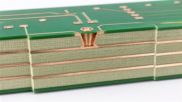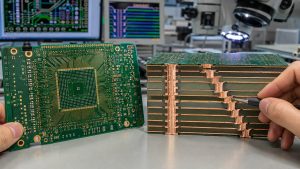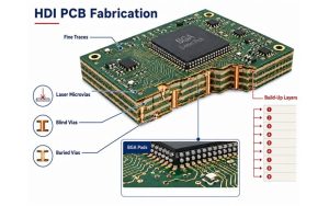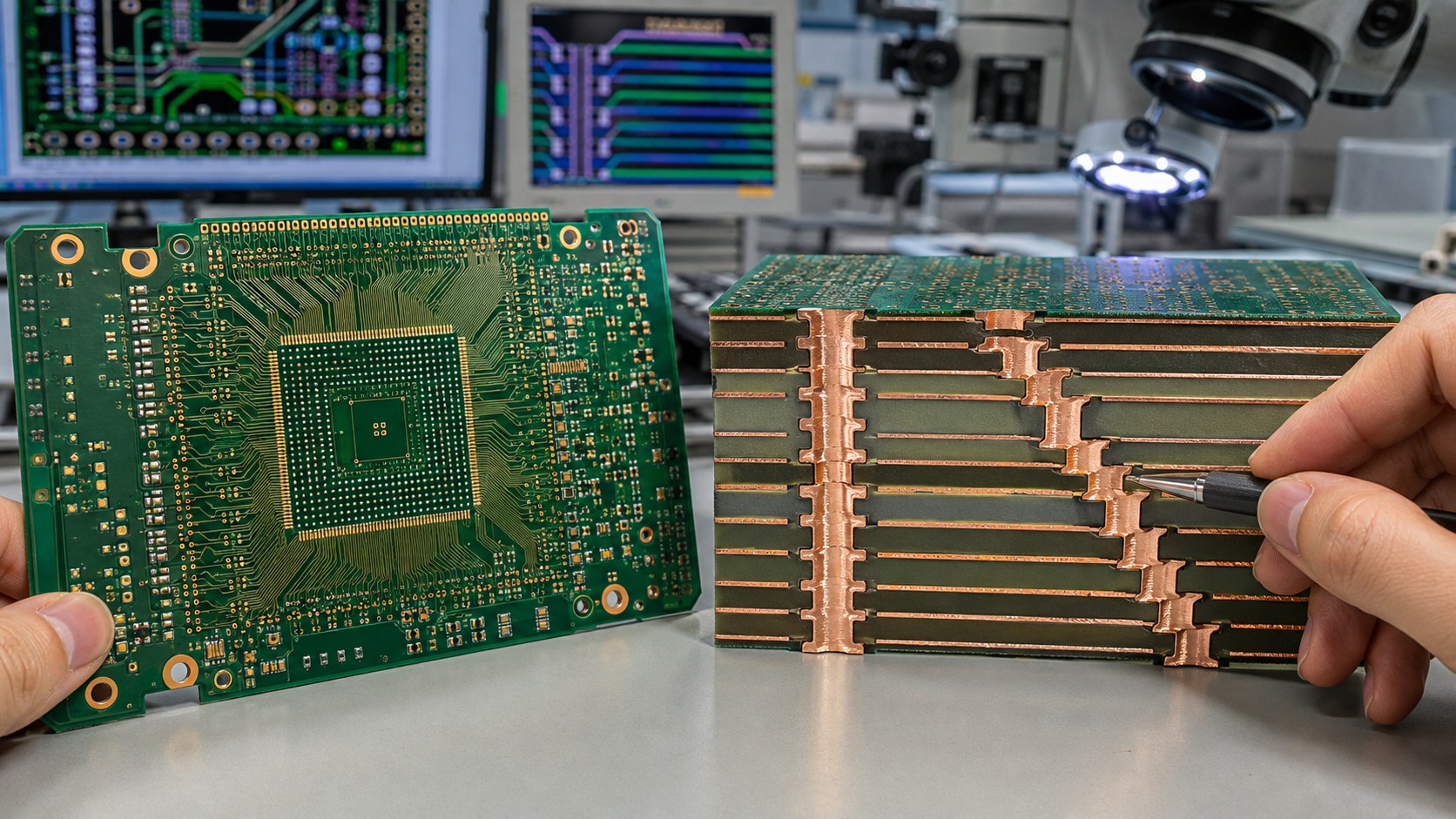
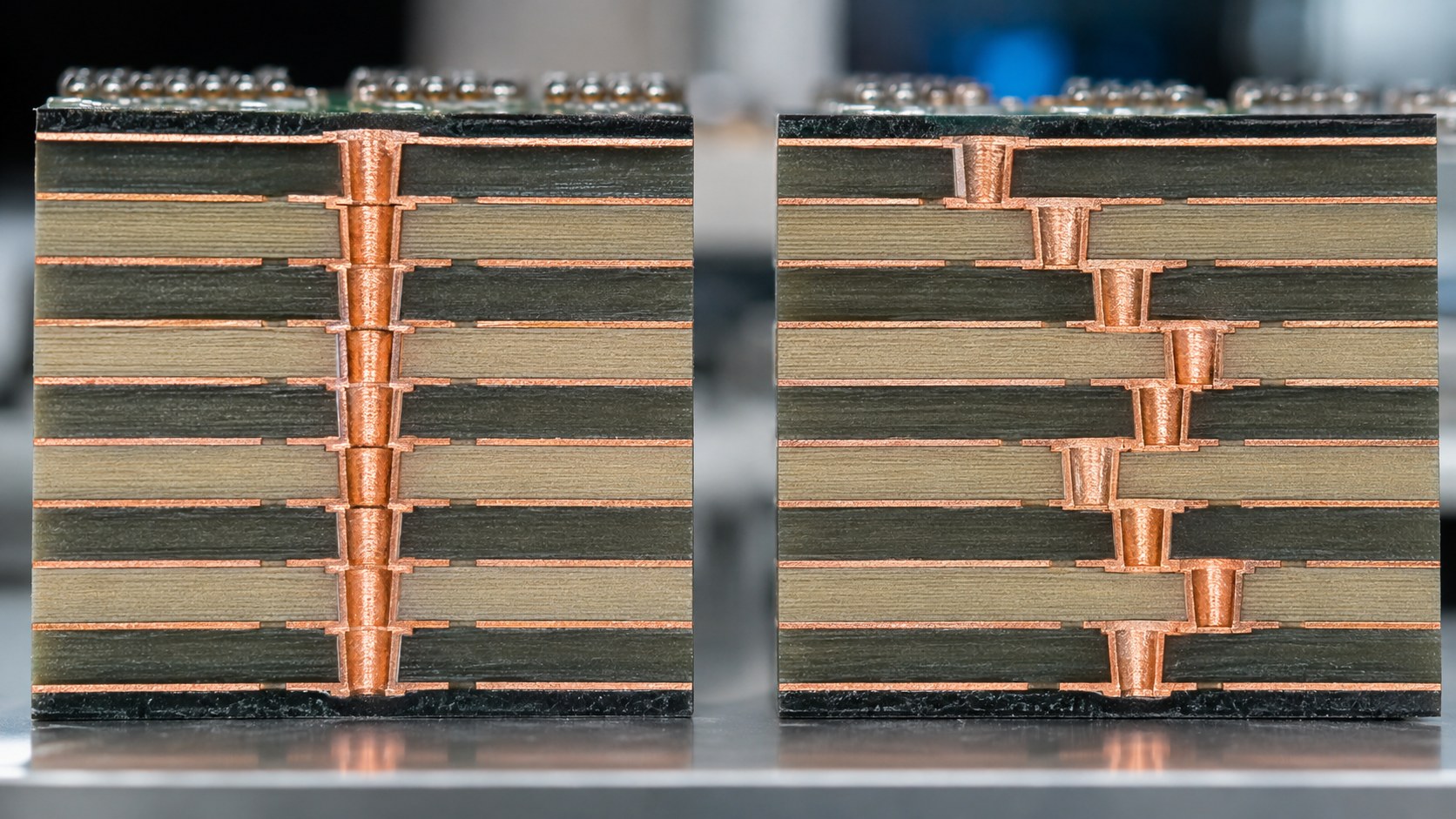
Stacked microvias align vertically through successive build-up layers, while staggered microvias step sideways from one layer transition to the next. Stacking preserves routing area and can support dense BGA escape, but it concentrates manufacturing interfaces in one column. Staggering needs more lateral space, yet it can simplify filling and reduce dependence on a long, perfectly aligned vertical structure.
The choice is not “advanced versus basic.” It should be made from the actual layer transitions, package pitch, routing channels, dielectric thickness, via geometry, assembly profile and the fabricator’s qualified HDI process.
Stacked vs Staggered Microvias at a Glance
| Decision factor | Stacked microvias | Staggered microvias |
| Routing area | Small vertical footprint | Needs lateral offset and landing space |
| Build dependency | Relies on aligned, filled underlying structures | Each transition lands on an offset capture pad |
| Process sensitivity | Higher sensitivity to fill, planarity and registration | More layout area but fewer vertical interfaces in one column |
| Typical reason to choose | Very dense escape or constrained routing corridor | Available area and preference for a less concentrated structure |
| DFM evidence | Stackup, fill plan, cross-sections and qualification data | Offset geometry, capture pads, registration and layer-clearance review |
This comparison is directional. Final geometry and permitted layer combinations must come from the selected manufacturer’s capability review, not from a universal online rule.
How Stacked and Staggered Microvia Structures Are Built
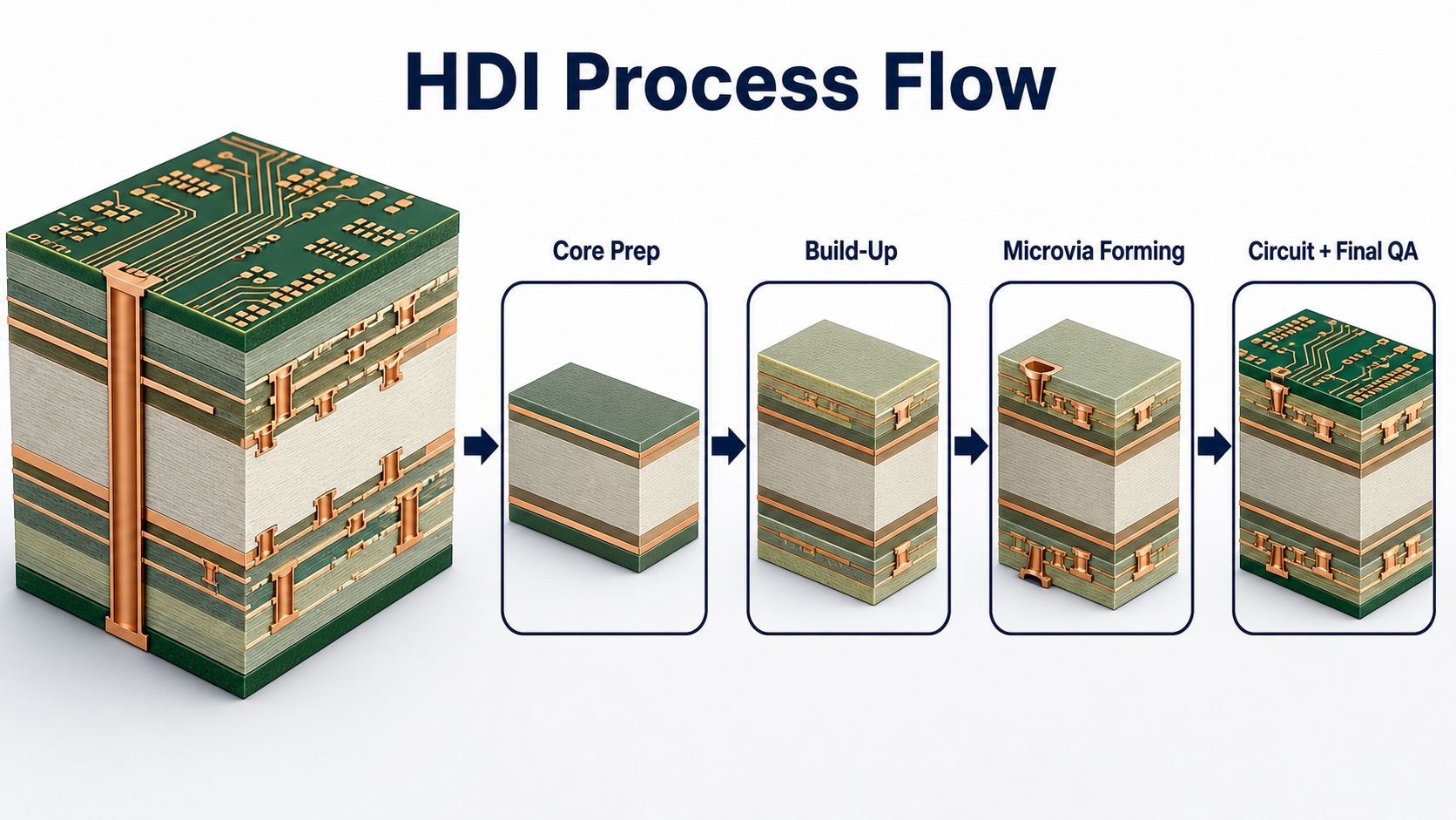
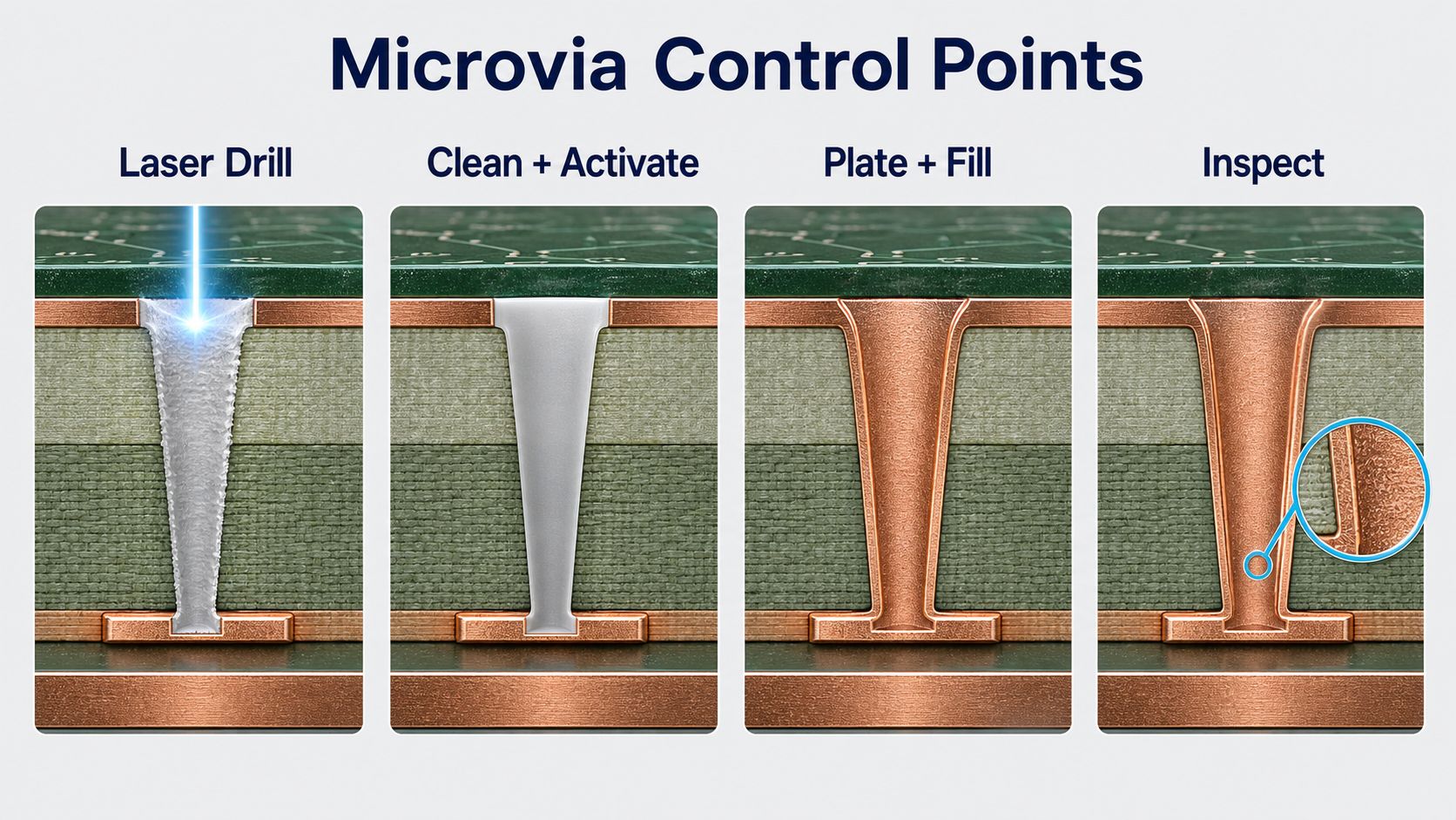
Both structures are created through sequential build-up: form one dielectric layer, laser-drill the microvia, metallize it, then repeat for the next layer transition. A stacked design places the next microvia directly over the filled and planarized structure below. A staggered design shifts the next via so it lands on a separate capture pad.
That sequence makes stackup communication essential. A drawing that only says “blind via” does not tell CAM which layers connect, whether vias stack, whether fill is required, or which structures carry critical signals.
Why Stacked Microvias Save Routing Area
A vertical stack uses less planar space than an offset chain. This can preserve escape channels under fine-pitch BGAs, shorten transitions and keep nearby routing available for power, ground or high-speed nets.
The density benefit is real only if the structure can be manufactured reliably. Adding more transitions to a column increases dependency on each laser-drill, metallization, fill, planarization and registration step. Designers should not stack automatically where a staggered route, buried via or different fanout could meet the same electrical task.
Why Staggered Microvias Can Simplify Reliability Control
Staggering distributes adjacent microvias laterally instead of building one continuous vertical column. When the package and routing area allow the offsets, it can reduce reliance on the surface of a filled microvia as the foundation for the next laser via.
The tradeoff is space. Every offset needs a valid capture pad, trace connection and clearance from adjacent features. A loose stagger can also make the route longer or consume a channel needed by another net.
Unsure whether your HDI transition should stack or stagger?
Send the BGA map, stackup, via table, critical nets and available escape geometry. EBest Circuit can review the structure before artwork release.
Reliability Risks That Need Attention in Stacked Structures
The most important risk is an imperfect interface inside a structure that depends on every layer transition. Incomplete copper fill, voids, depressed fill, weak interconnection, misregistration or material stress can accumulate through the column.
- A void or fill depression can affect the landing surface for the next microvia.
- Registration error can reduce the effective capture area at an interface.
- Repeated thermal excursions can stress copper-to-copper and copper-to-dielectric interfaces.
- Material expansion behavior influences strain during reflow and service.
- A structure that passes continuity may still require cross-sectional or reliability evidence.
Reliability cannot be inferred from the word “filled.” The specification should identify the stack, materials, acceptance criteria and required qualification evidence.
Capture Pads, Alignment, and Registration
Capture-pad geometry must tolerate the combined registration budget of imaging, lamination and laser drilling. A nominally centered CAD feature can lose effective land if process shifts align in the same direction.
For stacked vias, alignment must support the interface between successive features. For staggered vias, the offset must leave enough pad and connecting copper without violating spacing or blocking escape routes. Review finished geometry rather than judging only the drill file.
Related design foundations are covered in our PCB annular ring guide and microvia aspect-ratio guide.
Why Copper Filling and Planarization Matter
A microvia that supports another microvia generally needs a controlled filled and planarized surface. The next build-up layer must start from a stable landing condition. Fill voids, overfill, underfill or an uneven surface can affect imaging, lamination and the next laser-drilled feature.
Specify the required structure and acceptance result, then let the fabricator propose the qualified fill route. Do not substitute generic material names or assumed plating values for process evidence. Via-in-pad applications add assembly-flatness and solder-control concerns; see the VIPPO design and inspection guide.
Signal, Power, and Thermal Considerations
Geometry selection must serve the net, not only fabrication convenience. A compact stacked transition may reduce routing detour, but the complete return path, reference-plane change, anti-pad and nearby stitching strategy still determine electrical behavior.
For power paths, review current distribution and copper connection at every layer. Do not describe a microvia stack as a thermal solution without checking the complete heat path. Multiple distributed structures may behave differently from one concentrated column.
Cost and Lead-Time Drivers
Cost follows sequential build complexity, yield exposure, fill requirements, registration demands, inspection and qualification—not the via name alone. A dense stacked design may require more controlled cycles and evidence, while staggering may require a larger breakout region or another routing layer.
Ask for alternatives during DFM. A small fanout change, adjusted layer transition or mixed structure can reduce risk without changing the product function. Compare proposals using the same stackup and acceptance requirements.
Need a manufacturable microvia cost comparison?
Provide the current and acceptable alternative stackups, quantities, material needs, BGA pitch and inspection level. We can compare the real process impact.
Inspection and Qualification Evidence to Request
Use evidence that represents the actual microvia structure and production process. Useful controls can include coupon design, cross-sections, plating/fill review, registration checks, electrical test and agreed thermal-stress or reliability qualification.
The inspection plan should identify which stack is sampled, where coupons are placed, how interfaces are judged and what happens after a nonconformance. A generic statement that the board is electrically tested does not replace structural evidence.
Decision Checklist: Stack, Stagger, or Redesign the Transition
- Map every required layer transition from the actual net and BGA escape.
- Confirm how much lateral routing area is available.
- Identify which structures must align vertically and why.
- Review microvia geometry against each dielectric layer.
- Confirm capture pads, clearances, fill and planarization.
- Ask for the fabricator’s qualified structure and inspection evidence.
- Compare a staggered or mixed alternative before locking a tall stack.
- Freeze the approved via table, stackup and deviation process.
What to Send for EBest Circuit HDI DFM and Quotation
A useful RFQ connects design files to the exact microvia structure. Send Gerber or ODB++, drill/via data, fabrication drawing, stackup, material requirements, BGA package information, critical nets, controlled-impedance targets, quantities, assembly needs, inspection requirements and target delivery.
EBest Circuit can review whether the proposed stack, stagger or mixed strategy is clear and suitable for quotation, flag missing information and return project-specific questions. Any dimensional or process capability must be confirmed against the current build and approved factory route.
Stacked vs Staggered Microvia FAQ
What is the main difference between stacked and staggered microvias?
Stacked microvias align vertically; staggered microvias shift laterally between successive layer transitions.
Are staggered microvias always more reliable?
No. They can avoid a continuous vertical interface column, but reliability still depends on geometry, materials, process control and the actual design.
Why use stacked microvias?
They preserve routing area and can enable dense vertical transitions where the BGA escape or board outline leaves little lateral space.
Do stacked microvias need copper filling?
A microvia used as the landing foundation for another typically needs a qualified fill and planarization process. Confirm the exact structure with the fabricator.
How many microvias can be stacked?
There is no responsible universal answer. The permitted structure depends on the selected manufacturer’s qualified process, materials, dimensions and reliability requirements.
What is a microvia capture pad?
It is the copper land where the laser-drilled microvia terminates and connects to the target layer.
Can stacked and staggered microvias be mixed?
Yes, a board may use different structures where density and risk differ, provided the via table and stackup define them clearly.
Does electrical test prove a microvia stack is structurally reliable?
Electrical test confirms connectivity at test time; structural and reliability evidence may still be required for critical builds.
What data prevents microvia quotation errors?
Provide layer-pair definitions, stackup, hole/pad data, fill needs, quantities, materials, inspection criteria and any approved alternatives.
When should the fabricator review the microvia strategy?
Before layout constraints are frozen, and again before production release after the complete stackup and files are available.
Validate the HDI via structure before it becomes a yield problem.
Send your Gerber/ODB++, drill data, stackup, BGA map, materials, quantities and target delivery.