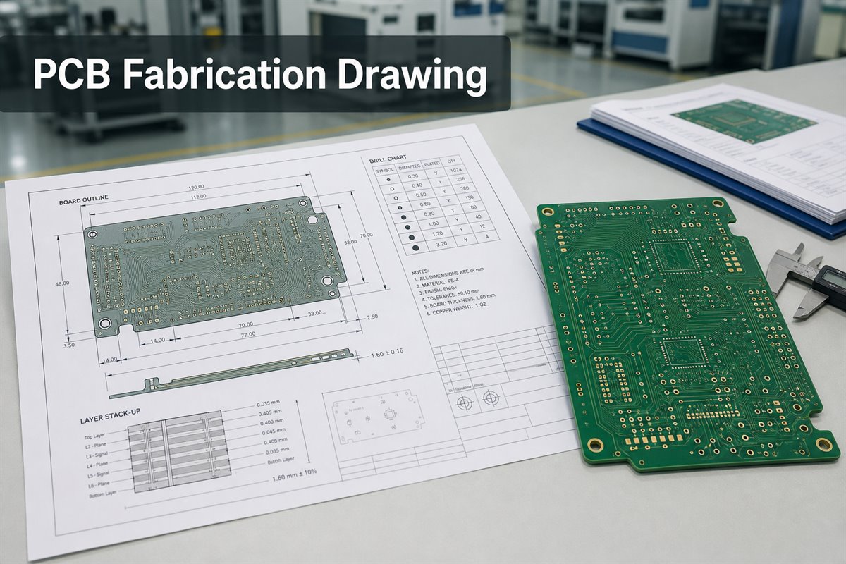
A clear PCB fabrication drawing puts the critical bare-board requirements in one controlled document. This guide shows what to include and what to check before release.
What Is a PCB Fabrication Drawing?
A PCB fabrication drawing defines how a bare printed circuit board must be built and accepted. It combines a dimensioned board view with manufacturing notes, tolerances, drill information, layer construction, and revision data.
It does not replace Gerber or ODB++ data, NC drill files, or other production outputs. Those files provide artwork and machine-readable data. The drawing adds requirements that may not be clear from the artwork alone.
A controlled drawing helps the customer:
- Reduce questions during quotation.
- Keep suppliers on the same requirements.
- Control the approved design revision.
- Resolve file discrepancies before production.
Use the released design—not an old prototype or requirements left in an email thread.
The drawing also gives purchasing, engineering, and quality teams one reference during supplier comparison. When two quotations differ, the team can check whether both suppliers priced the same material, construction, tolerances, finish, inspection, and test scope instead of comparing price alone.
PCB Fabrication Drawing vs PCB Assembly Drawing
A fabrication drawing controls the bare board. A PCB assembly drawing controls component placement and orientation. Mixing them can cause the fabrication or assembly team to miss critical information.
| Document | Controls | Key content |
| Fabrication drawing | Bare board | Outline, holes, stack-up, finish, tolerances |
| Assembly drawing | Component installation | Designators, polarity, orientation, mounting notes |
| BOM and placement data | Parts and coordinates | Part numbers, quantities, X-Y data, rotation |
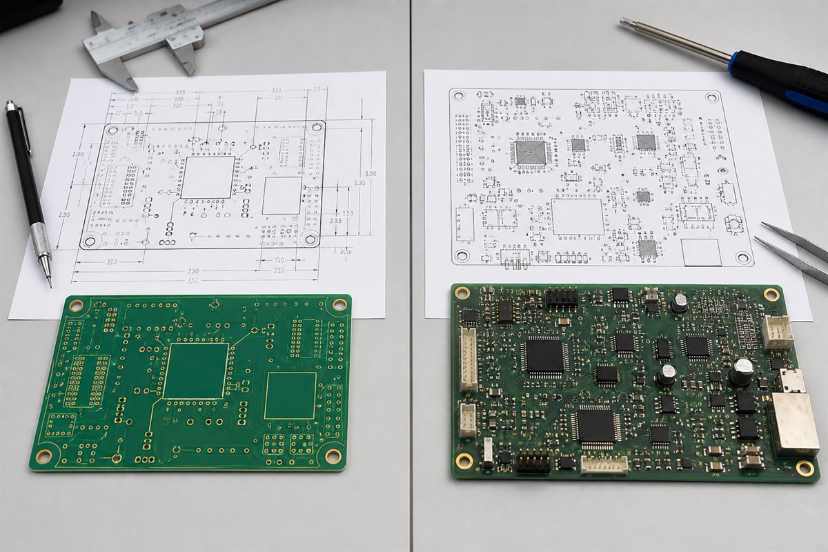
The release rule is simple: the fabrication drawing answers, “What bare board must be made?” The assembly drawing answers, “What must be installed, and how?” If information appears in both, confirm that the values and revisions match.
What Should a PCB Fabrication Drawing Include?
The exact content depends on board complexity. However, the fabricator should be able to quote, plan, build, and inspect the board without inventing missing requirements.
Include these essentials:
- Board outline, dimensions, datum, cutouts, notches, and critical edge features.
- Finished thickness and tolerance.
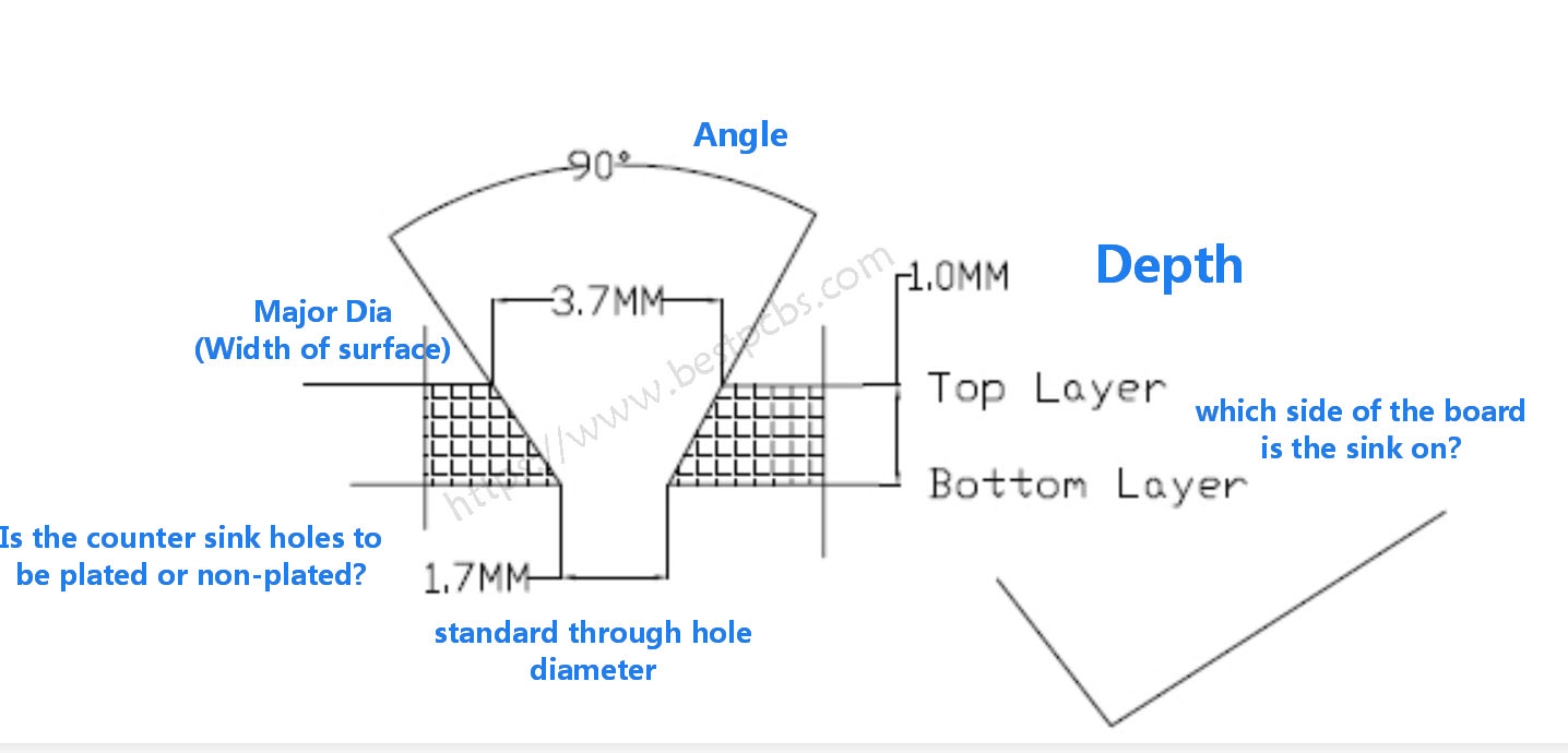
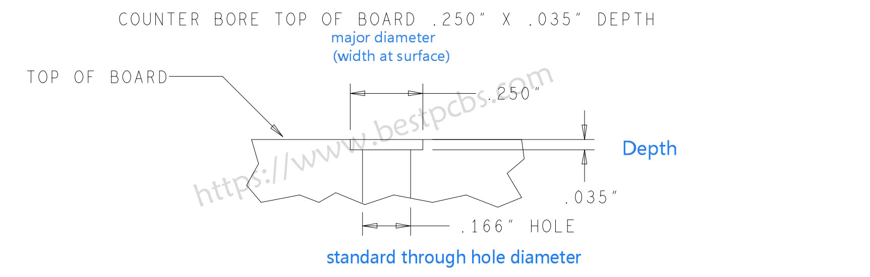
- Finished hole sizes, plated status, slots, and special tolerances.
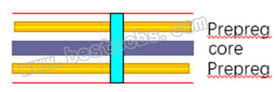
- Layer count, order, material, dielectric construction, and copper weight.
- Controlled-impedance targets, layers, and tolerances.
- Solder mask, silkscreen, surface finish, and special processes.
- Agreed inspection, electrical-test, coupon, or report requirements.
- Part number, drawing number, revision, date, units, and approvals.
Avoid copying a generic note set into every design. Remove requirements that do not apply, and add approved special requirements to the controlled package.
PCB Fabrication Drawing Notes That Prevent Production Assumptions
PCB fabrication drawing notes should clarify details that geometry cannot communicate. Effective notes stop the supplier from using a default value that may affect cost, lead time, reliability, or fit.
Useful notes may define:
- Finished dimensions versus pre-plating tool sizes.
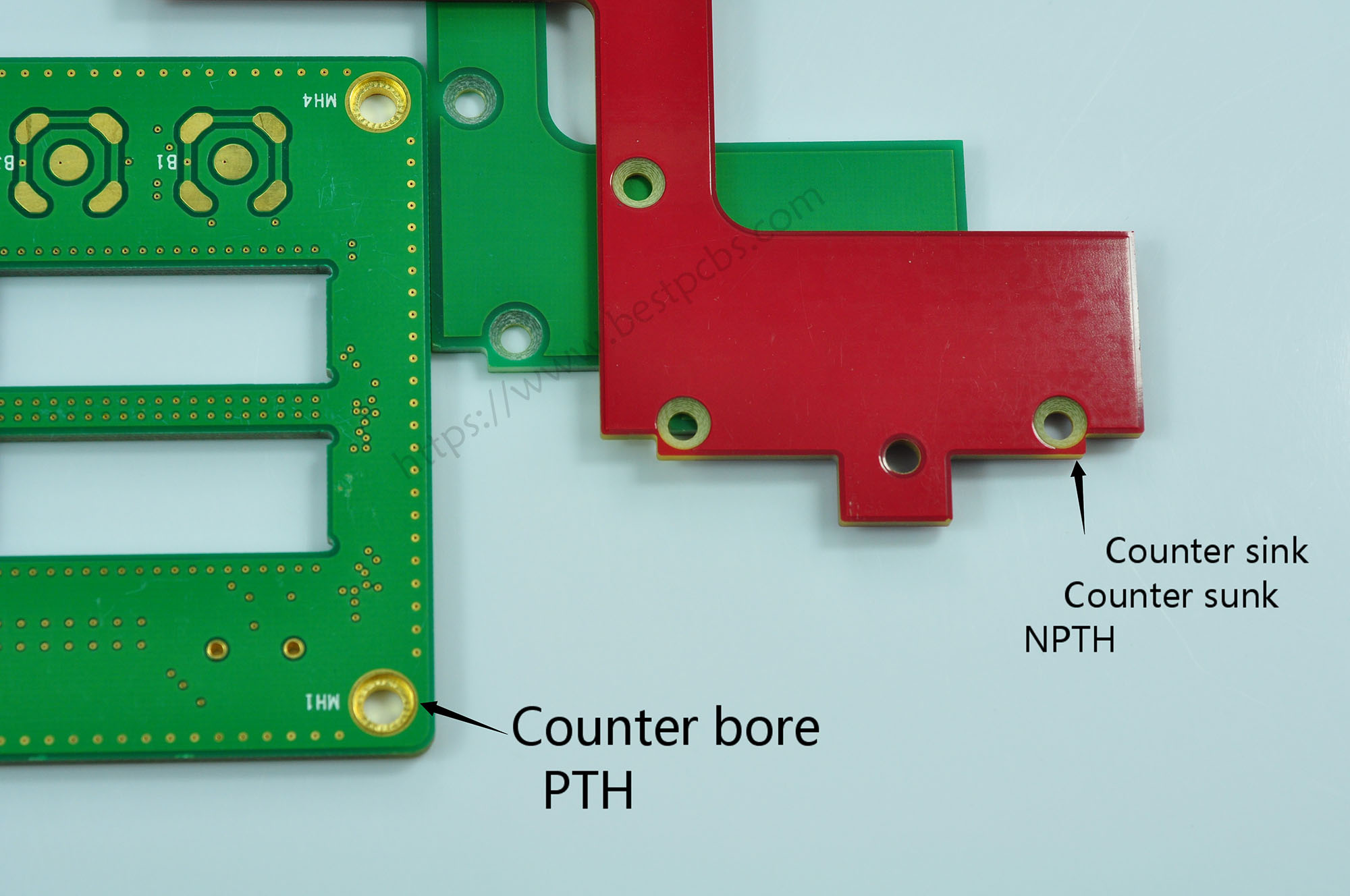
- Plated, non-plated, press-fit, or tightly controlled holes.
- Mandatory materials and permitted alternatives.
- Starting or finished copper weight.
- Solder mask, legend, finish, and special coatings.
- Controlled-impedance requirements.
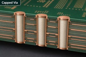
- Filled or capped vias, via-in-pad, edge plating, or castellations.
- Electrical testing and required quality records.
- The required action when files disagree.
Use measurable requirements. “Manufacture to the highest quality” cannot be inspected. State the expected result and acceptance condition instead.
How to Check a PCB Fabrication Drawing Against Manufacturing Files
Many release failures come from conflicting documents. A drawing may show revision C while the Gerber package came from revision B. A drill table may not match the NC drill file. A six-layer stack-up may not match the supplied artwork.
Check the complete package before RFQ:
- Match part numbers and revisions across all files.
- Compare the board outline, cutouts, slots, and dimensions.
- Match the drill chart to the NC drill data.
- Confirm plated and non-plated hole definitions.
- Compare layer count and order with the copper files.
- Check material, copper, thickness, finish, mask, and legend.
- Confirm impedance layers, targets, and tolerances.
- Remove obsolete outputs from the release package.
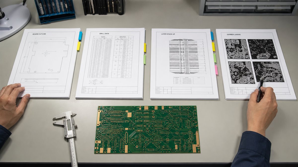
Stop the release when the drawing and electronic data disagree. The fabricator can identify a conflict and suggest an option, but the customer must confirm the intended requirement.
Tolerances and Acceptance Requirements in a PCB Drawing
A nominal dimension without a tolerance can cause a conservative quote or a board that fails an unstated fit requirement.
A PCB drawing should identify tolerances where variation affects fit, function, assembly, or inspection. Common examples include board thickness, routed outline, finished holes, slot width, connector edges, and enclosure interfaces.
| Feature type | Customer decision | Result |
| Critical fit | Define tight tolerance | Protects mounting and mating |
| Electrical | Define performance limit | Controls impedance or testing |
| Non-critical | Use standard capability | Avoids unnecessary cost |
Do not tighten every dimension. Tighter tolerances can increase process control, inspection, cost, and yield risk.
If an IPC class, customer specification, impedance report, or test requirement applies, identify the approved document and revision. The customer owns the final product-level acceptance criteria and approves any proposed change.
Revision Control for a PCB Fab Drawing
Revision errors can place a correct design into production under an obsolete specification. The risk increases when drawings, Gerbers, drill files, and purchase orders are stored separately.
A PCB fab drawing should show the part number, drawing number, revision, release date, units, and approval status. Use the same revision identity across the manufacturing package.
Before release:
- Assign one package owner.
- Generate outputs from the approved PCB source.
- Store related files in one controlled folder.
- Remove superseded files.
- Record approved supplier questions and changes.
- Reference the approved revision on the purchase order.
Avoid filenames such as final, final-new, or latest. They do not provide reliable production control.
A PCB Fabrication Drawing Example Before Production Release
Consider a six-layer control board that fits inside a machined enclosure. The Gerber and drill files are complete, but the initial drawing lists only the overall dimensions and board thickness.
During review, the fabricator finds three gaps:
- No finished tolerance for the connector holes.
- No finished width for a routed slot.
- No layer-specific impedance target.
| Stage | Drawing status | Production effect |
| Before correction | Critical details missing | Questions and fit risk |
| After correction | Dimensions and impedance defined | Clear quote and inspection basis |
The customer updates the controlled drawing and releases it with the matching manufacturing files. This PCB fabrication drawing example shows why project-specific risks matter more than a long generic checklist.
How EBest Reviews PCB Fabrication Data Before Quotation
EBest Circuit (Best Technology) can review the submitted package for fabrication completeness and manufacturability. The review may identify missing stack-up information, unclear hole requirements, data conflicts, or special features that need confirmation.
For an efficient review, provide:
- Approved PCB fabrication drawing.
- Gerber, ODB++, or other agreed fabrication data.
- NC drill and routing files.
- Stack-up and impedance requirements.
- Material, copper, thickness, mask, and finish requirements.
- Quantity and requested lead time.
- Agreed inspection, test, report, or traceability needs.
EBest may propose a manufacturable stack-up, material alternative, or tolerance adjustment. The customer must approve the change before production.
For PCBA quotations, also provide the BOM, placement data, assembly drawing, inspection criteria, and agreed test inputs. EBest supports PCB fabrication, DFM, sourcing, PCBA, inspection, and agreed testing coordination. The customer owns circuit performance, design intent, firmware, certification, and final product validation.
FAQs About PCB Fabrication Drawings
Is a PCB fabrication drawing required if Gerber files are complete? It is recommended when material, tolerance, impedance, finish, special-process, or acceptance requirements are not fully defined by the Gerber data.
Can a PCB fabrication drawing replace Gerber and NC drill files? No. The drawing defines manufacturing requirements. Gerber, ODB++, IPC-2581, NC drill, and routing files provide detailed production data.
Should fabrication and assembly information be on one drawing? Separate drawings are usually clearer. The fabrication drawing defines the bare board; the assembly drawing defines component installation.
Who resolves a conflict between the drawing and Gerber data? The fabricator should report the conflict. The customer or authorized design owner must confirm the requirement before production.
What files should be sent for a PCB quotation? Send the drawing, fabrication data, drill and routing files, stack-up, impedance requirements, material and finish specifications, quantity, and lead-time request.
Ready to request a PCB or PCBA quotation? Send your approved PCB fabrication drawing, manufacturing files, quantity, and target lead time to sales@bestpcbs.com. EBest Circuit will review the package and identify any missing or conflicting fabrication requirements before quotation.