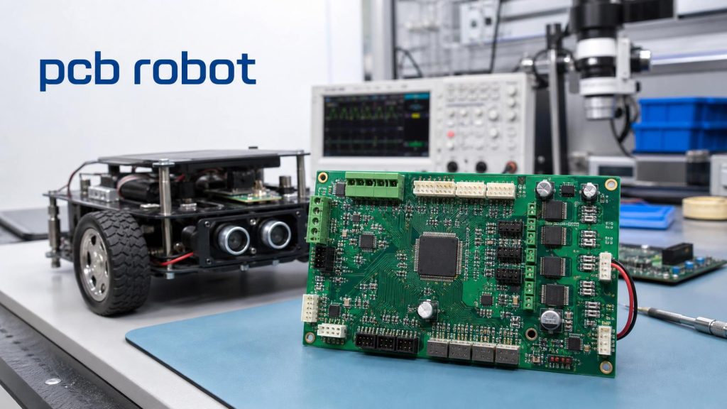
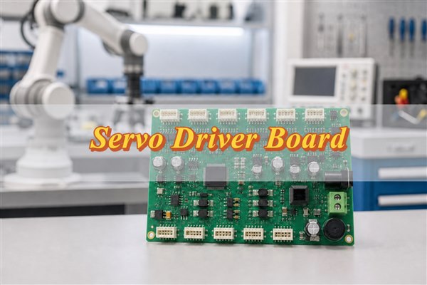
A line tracing robot PCB board must read optical contrast while two motors generate electrical noise, then convert those readings into stable steering commands. Production readiness depends on four controlled relationships: sensor geometry to the chassis, motor current to the power network, firmware to the hardware revision, and functional-test limits to the finished assembly.
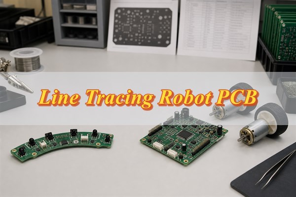
Are you worried about your line tracing robot PCB board project?
- Will sensor height, pitch, or alignment changes after assembly make a proven prototype track inconsistently?
- Could motor startup, reversal, or stall current reset the MCU or corrupt the optical sensor readings?
- Will mismatched PCB, BOM, firmware, and test revisions delay the quotation or create avoidable rework in production?
With 20 years of PCB and PCBA manufacturing experience, EBest Circuit provides one-stop support from production-data review through assembly and functional-test preparation.
- Protect installed sensor geometry: Submit the PCB outline, sensor locations, mounting-hole datums, wheel-axis reference, and target sensor-to-track height. We review these controlled relationships with the fabrication and assembly data before production release, helping your team catch drawing conflicts before boards are built.
- Control motor-power interference: Provide the battery range, motor running and stall current, driver part number, copper requirements, and critical sensor or reset limits. Our engineering review checks high-current paths, driver thermal features, decoupling placement, return paths, and test access so the prototype build can be evaluated under realistic motor transients.
- Keep production inputs aligned: Release identified revisions of the Gerber or ODB++, fabrication drawing, BOM, centroid file, assembly drawing, firmware, calibration method, and functional-test limits. We compare the package before sourcing and assembly, then raise conflicts for approval rather than guessing at missing requirements.
Ready to start your line tracing robot PCB board project? Send your design files, BOM, quantities, stackup, firmware or programming scope, and test requirements to sales@bestpcbs.com for an engineering review and quotation.
What Does a Line Tracing Robot PCB Board Control?
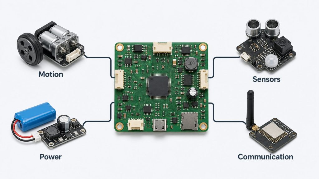
The board measures the line position and converts the position error into separate left- and right-motor commands. A typical signal path is infrared emitter, photodetector, analog or timed input, MCU calculation, PWM output, motor driver, and motor. The PCB must support each interface without allowing the motor-current path to disturb the sensor reference.
Sensor channels first require calibration because emitter output, detector response, height, and track reflectivity vary. Firmware can normalize the channels, assign each sensor a position, and calculate a weighted line location. The difference between that location and the target center becomes the steering error. A proportional or PID-style routine then adjusts the two motor commands.
Freeze the operating behavior before schematic release. Define what happens when the line is lost, all channels saturate, a junction covers several sensors, a motor stalls, or battery voltage falls. These conditions determine MCU resources, fault inputs, driver selection, memory use, and factory-test coverage. A dedicated IR sensor PCB design review can support the emitter, detector, and receiver-interface decisions.
Should a Line Tracing Robot Use One PCB or Separate Control and Sensor PCBs?
Use one PCB for a compact robot with fixed sensor geometry; split the sensor and control circuits when the sensor bar must move, be replaced, or support several chassis variants. This is primarily a mechanical, service, and signal-integrity decision—not a preference for fewer or more boards.
- Choose one PCB: The sensor height and forward offset are fixed, the board fits the chassis, and removing a cable and connector improves cost and reliability.
- Choose two PCBs: The sensor bar needs independent height adjustment, is exposed to impact or dirt, or must be reused with different controller and motor configurations.
- Control the interconnect: Specify connector family, pinout, cable length, retention, bend direction, current rating, shielding or ground conductors, and assembly orientation.
- Share one datum system: Dimension the sensor centerline, wheel axis, mounting holes, and chassis references from matching origins on the PCB and mechanical drawings.
For a split design, keep local sensor filtering and any required analog reference close to the detector array. Do not route sensitive sensor outputs beside motor leads in the same cable without reviewing return paths and coupling. Prototype the complete cable and connector arrangement because a sensor board that works on a bench can become noisy after installation beside the motors.
How Does Sensor Placement Affect Line Tracing Robot Tracking Accuracy?
Installed sensor pitch, height, forward offset, and tilt determine what the control algorithm can measure. A layout may be electrically correct yet track poorly if the assembled array sits outside the optical range or moves relative to the wheel axis.
Choose the sensor-array width and channel pitch from the actual line width, minimum curve radius, target speed, and required steering resolution. Sensors placed too far apart can leave gaps in position information, while an unnecessarily tight pitch adds channels without correcting poor mechanical alignment. Evaluate the intended track materials because dark and light surfaces can produce different contrast margins.
Control sensor height from the running surface rather than from the bare PCB alone. Wheel diameter, tire compression, spacers, solder-joint height, board thickness, and chassis tolerance can all change the installed distance. Put the sensor centerline, wheel axis, and mounting holes on one mechanical datum system so PCB and chassis drawings cannot define conflicting positions.
Forward offset also changes steering behavior. A larger distance between the sensor array and wheel axis gives the controller earlier information about a curve, but it can amplify mechanical error and require different control tuning. Confirm the offset on the assembled robot instead of relying only on PCB dimensions.
Finally, keep board edges, fasteners, tall components, covers, and cable shadows outside the optical field. Define clean handling and inspection for emitter and detector windows, then verify the complete assembly under the expected ambient light—not only under controlled bench lighting.
How Should Sensor, MCU and Motor Driver Circuits Be Arranged on the PCB?
Partition the layout into a quiet sensor zone, a digital control zone, and a compact motor-power zone. Component placement should control current paths before detailed routing begins.
- Place the sensor front end: Keep receiver filters, pull resistors, reference components, and any analog conditioning close to the sensor inputs. Protect these nodes from motor outputs, switching nodes, PWM traces, and high-current connector pins.
- Group the MCU support circuit: Place clock, reset, boot, and local bypass components near their assigned MCU pins. Keep the programming interface accessible without routing it through the optical sensing area.
- Compact the motor-power loop: Place the motor driver beside its high-frequency bypass capacitors and motor connector. Minimize the loop formed by the supply capacitor, driver power stage, motor output, and return path.
- Control return current: Maintain a continuous signal reference where practical and use component placement to keep motor current away from sensor and MCU returns. Avoid arbitrary ground splits that force signals to cross gaps or take longer return paths.
- Design the thermal path: Match exposed-pad copper, thermal vias, solder-mask openings, and paste apertures to the driver package and expected power loss. Confirm that the proposed structure can be fabricated, printed, reflowed, and inspected consistently.
- Reserve test access: Provide reachable points for battery input, regulated rails, ground, reset, programming, driver fault, and representative sensor channels. Check fixture approach in the mechanical model so probes cannot collide with wheels, connectors, covers, or the sensor field.
How Can a Line Tracing Robot PCB Reduce Motor Noise and Power Instability?
Design the power network for motor start, reversal, braking, and stall rather than nominal running current. Size the connector, protection device, copper path, driver, regulator, and capacitance from the verified motor and battery limits with engineering margin.
Keep each switching-current loop short and place driver bypass components at the specified power pins. Do not share narrow return paths between motors and sensors. Separate motor outputs from sensor traces and oscillators, and decouple the MCU and sensor rail locally.
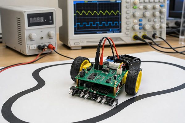
Validate the assembled prototype with an oscilloscope during start, stop, reversal, and stall-current limiting. Monitor battery input, regulated rails, MCU reset, sensor reference, and driver fault. A stable bench supply at idle does not prove the board will remain stable on the robot.
Which Line Tracing Robot PCB Board Specifications Should Be Confirmed Before Production?
Confirm the complete board construction and acceptance requirements in one controlled fabrication drawing before production. The drawing must agree with the Gerber or ODB++ data; conflicting notes create quotation delays and force the manufacturer to request clarification.
- Board construction: State layer count, material family, finished thickness, stackup, copper weight by layer, and any controlled-impedance requirement.
- Fabrication geometry: State minimum trace and spacing, finished-hole sizes, annular-ring expectations, routed slots, cutouts, castellations if used, and the finished outline tolerance.
- Surface requirements: Specify the surface finish, solder-mask color and sides, legend color and sides, carbon or other special finishes, and areas that must remain free of mask or legend.
- Mechanical controls: Identify the datum scheme, mounting-hole locations, sensor-edge relationship, connector position, profiling method, and any thickness or flatness constraint that affects the chassis.
- Electrical acceptance: Define bare-board electrical testing, impedance coupons when applicable, netlist source, and any special isolation or high-current checks.
- Panel and marking data: Define panel size or permit the manufacturer to propose it, then state tooling holes, fiducials, breakaway method, board identification, date code, and traceability needs.
The supplied EBest capability workbook lists general FR-4 references including up to 10 layers, 4/4 mil line and spacing with 1 oz copper, and a 0.2 mm minimum finished hole. These figures define review boundaries, not recommended values for every robot PCB. Select the released rules from motor current, voltage drop, annular-ring margin, board stiffness, routing density, assembly yield, and repeat-order stability; submit tighter features for engineering confirmation before quotation.
Which Components Require Special Controls During Line Tracing Robot PCB Assembly?
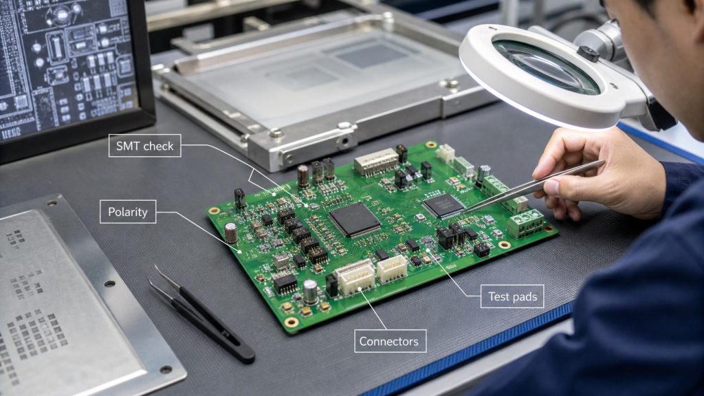
Optical sensors, thermal-pad motor drivers, polarized parts, connectors, and programming interfaces need explicit assembly controls. Their orientation, height, placement, or soldering can determine system function even when general workmanship is acceptable.
- Optical sensors: Control the exact manufacturer part number, orientation, mounting height, coplanarity, window cleanliness, and any light barrier or cover that changes the field of view.
- Motor drivers: Follow the component land pattern, thermal-pad via design, paste-window recommendation, polarity marking, and reflow limits; verify exposed-pad soldering with the agreed inspection method.
- Polarized parts: Make diode, electrolytic-capacitor, LED, IC, and connector polarity unambiguous in the centroid file, assembly drawing, silkscreen, and first-article inspection.
- Mechanical connectors: Check mating direction, latch access, cable exit, solder-joint support, insertion force, and clearance from wheels, batteries, and covers.
- Programming interfaces: Reserve probe access and define pad finish, pitch, datum, keepout, and fixture approach so programming does not rely on hand-held wires.
Supply exact manufacturer part numbers, approved alternatives, centroid data, assembly drawings, and variant rules. A substitute optical sensor can change spectral response or package height even when its footprint fits; a substitute motor driver can change current limiting, decay behavior, pin functions, or thermal needs. Require approval before either part is changed.
How Is a Line Tracing Robot PCB Board Manufactured and Assembled?
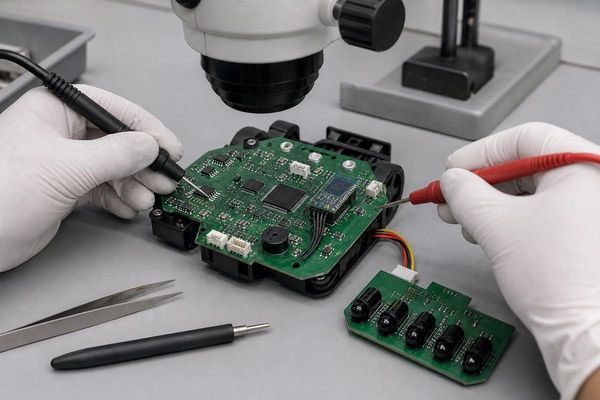
A line tracing robot PCB board moves through controlled data review, bare-board fabrication, assembly, inspection, programming, calibration, and functional testing. Each stage must use the same approved hardware, BOM, firmware, and test revisions.
- Review the production data: Compare Gerber or ODB++, drill files, fabrication notes, stackup, BOM, centroid data, assembly drawings, panel requirements, firmware, and test instructions. Resolve conflicting revisions, missing polarity, unsupported components, and unclear tolerances before material is released.
- Fabricate the bare PCB: Image and etch the copper layers, laminate multilayer constructions when required, drill and plate the holes, apply solder mask and legend, add the specified surface finish, and profile the board outline.
- Verify the bare board: Complete electrical testing against the supplied netlist and inspect dimensions, holes, slots, finish, markings, and workmanship. Controlled-impedance designs also require the agreed coupon and measurement records.
- Prepare the assembly line: Verify the released BOM and PCB revision, inspect incoming components, load the approved placement program, confirm stencil and paste requirements, and check feeder setup against polarity and package data.
- Place and solder components: Print solder paste, inspect the deposits when SPI is specified, place surface-mount parts, and run the validated reflow profile. Solder through-hole motor connectors, switches, or battery terminals in the specified secondary process.
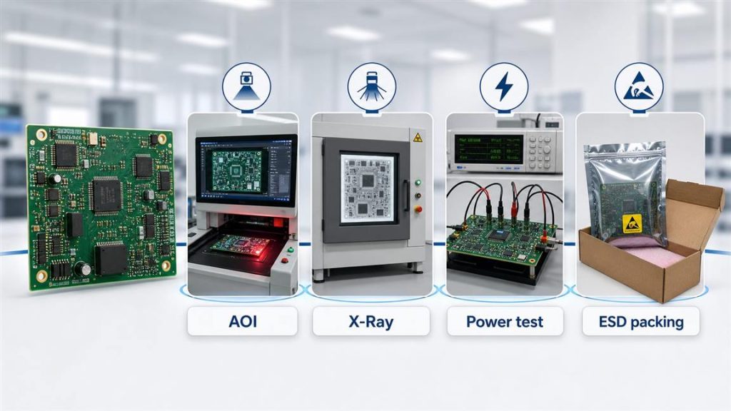
- Inspect the assembled PCBA: Use AOI and appropriate manual or X-ray inspection to check presence, polarity, alignment, solder joints, exposed pads, and hidden connections. Record and disposition defects instead of passing reworked boards without traceability.
- Program and calibrate the board: Load the approved firmware, verify its checksum, apply configuration data, and expose every sensor channel to the defined light and dark references. Store or record calibration values according to the released method.
- Complete functional testing: Check input power, regulated rails, MCU operation, every sensor channel, left and right motor outputs, driver faults, and protection behavior against written limits. SPI and AOI confirm process conditions, but only functional testing demonstrates that the programmed assembly can control the robot.
How Should a Line Tracing Robot PCB Board Be Functionally Tested?
Functional testing must verify the programmed PCBA from power input through sensor response, motor control, fault handling, and real tracking behavior. Bare-board electrical test and AOI remain necessary, but they cannot prove that the finished assembly controls the robot correctly.
- Confirm the tested configuration: Read the PCB revision, BOM variant, firmware checksum, configuration version, and unit or lot identifier. Test only combinations approved in the hardware-firmware compatibility matrix.
- Measure power and startup: Apply the specified input range with current limiting, then check input current, regulated rails, reset behavior, and startup stability. Include polarity, undervoltage, or other protection functions only when they are part of the released design.
- Test sensors and calibration: Apply controlled light and dark references to every channel, confirm channel order, and compare readings with written limits. Run calibration at the specified sensor height and ambient-light condition, then verify that stored values can be recalled after a power cycle.
- Exercise motors and faults: Test left and right outputs independently with the specified motors or validated loads. Verify direction, PWM response, braking or coast behavior, current limiting, connector pinout, and driver-fault reporting; apply only safe fault conditions defined by the test plan.
- Run the assembled robot: Test with the released battery, motors, wheels, sensor height, axle offset, and cable routing. Use representative straight lines, curves, transitions, and line-loss conditions at the target speed so mechanical and control interactions are included.
- Save the acceptance record: Record measured values, limits, pass or fail status, firmware checksum, fixture revision, unit or lot identity, and rework status. This evidence must distinguish a programming, calibration, assembly, or component failure if the unit is investigated later.
How Can a Line Tracing Robot PCB Prototype Be Prepared for Volume Production?
Prepare a line tracing robot PCB prototype for volume production by replacing every temporary build decision with released data, repeatable tooling, and measurable acceptance criteria. A prototype that follows a track once is not yet a production baseline; the team must prove that the PCB, components, assembly process, firmware, calibration, and final robot mechanics can be reproduced without individual hand adjustment.
- Remove prototype-only hardware: Replace flying wires, plug-in development modules, hand-soldered jumpers, temporary connectors, and manually added capacitors with documented schematic and PCB changes. If a modification remains necessary, include it in the controlled design rather than leaving it as an operator instruction.
- Freeze compatible revisions: Assign released revisions to the schematic, PCB data, fabrication drawing, BOM, centroid file, assembly drawing, firmware, mechanical drawing, calibration method, and test specification. A compatibility matrix should identify which firmware and BOM variant belongs to each PCB revision.
- Confirm component availability: Review optical sensors, MCU, motor driver, regulator, connectors, and other critical parts for lifecycle status, package consistency, lead time, minimum order quantity, and approved alternatives. Test any substitute that can change sensor response, component height, current limiting, pinout, or thermal behavior before adding it to the BOM.
- Complete DFM and assembly review: Confirm trace and hole rules, annular rings, solder-mask clearances, copper balance, component spacing, polarity markings, paste apertures, thermal-pad design, connector access, and board-edge clearances. Resolve exceptions before the production panel and stencil are released.
- Prepare panel and machine features: Add panel fiducials, tooling holes, breakaway rails, board identification, and a depaneling method that does not bend the sensor area or damage edge-mounted connectors. Verify that panel orientation supports paste printing, placement, inspection, soldering, and fixture loading.
- Replace manual setup with fixtures: Provide stable access for programming, power, ground, reset, representative sensor channels, motor outputs, and driver faults. Calibration fixtures must reproduce the specified sensor height, optical reference, ambient-light condition, and board orientation instead of relying on an operator holding a target by hand.
- Run a production-representative pilot build: Use the intended PCB panel, stencil, placement program, reflow profile, through-hole process, programming file, calibration routine, and functional-test limits. Include the released motors, battery range, cable routing, sensor-to-track height, and chassis datums when verifying complete tracking behavior.
- Close defects before scaling quantity: Record solder defects, programming failures, calibration outliers, motor-channel faults, tracking failures, rework time, and component losses by cause. Correct the design or process, update every affected file, and repeat the necessary tests instead of treating successful rework as proof that the original process is ready.
- Approve the production baseline: Retain the accepted first article or golden sample with its PCB revision, BOM, firmware checksum, calibration data, fixture revision, and test record. Repeat orders should use this controlled baseline, with customer approval and defined retesting for subsequent engineering changes.
Before releasing a larger order, require evidence that the pilot build used production-intent materials and processes, that every unit passed the written acceptance limits, and that open deviations have owners and closure dates. This prevents a low prototype price from turning into recurring rework, inconsistent tracking performance, or an avoidable schedule delay during volume production.
What Files and Specifications Are Required for a Line Tracing Robot PCB Board Quote?
A complete quotation package must define fabrication, assembly, sourcing, programming, calibration, and testing scope. Gerber files alone cannot describe a production-ready PCBA.
- PCB data: Gerber and drill files or agreed ODB++, fabrication drawing, and stackup requirements.
- Assembly data: BOM, centroid file, assembly drawings, polarity, and approved alternatives.
- Mechanical data: Outline, datums, sensor height, chassis relationship, and connector constraints.
- Firmware data: Released binary, checksum, target, programming method, and protection settings.
- Test data: Calibration references, loads, limits, fixture responsibility, and required records.
- Order scope: Prototype and forecast quantities, supplied parts, packaging, and delivery destination.
How Should You Choose a Line Tracing Robot PCB Manufacturer?
Choose a manufacturer by the risks it can remove from your prototype-to-production transfer, not by PCB price alone. The supplier should show how its controls protect tracking performance, revision accuracy, component availability, and delivery consistency.
- Protect the sensor geometry: Confirm that the manufacturer reviews sensor pitch, height references, board outline, mounting holes, and connector positions against the mechanical drawing before fabrication.
- Prevent power-related redesigns: Ask for review of motor-current paths, copper requirements, driver thermal features, regulator loading, and test access before the first production panel is released.
- Control component substitutions: Require approval before changing optical sensors, motor drivers, connectors, regulators, or other parts that can alter function, height, pinout, or thermal performance.
- Keep every revision aligned: The quotation, fabrication data, BOM, centroid file, firmware, calibration method, and test procedure should identify compatible revisions. This reduces the risk of assembling the correct components on the wrong PCB version.
- Define measurable acceptance: Request the proposed inspection, programming, calibration, and functional-test flow. The supplier should explain which results are recorded and how failed or reworked units remain traceable.
- Evaluate production support: Look for useful DFM feedback, clear responsibility for fixtures and supplied parts, documented issue approval, and a repeat-order process that preserves approved materials and settings.
Why Choose EBest Circuit for Line Tracing Robot PCB Board Manufacturing?
EBest Circuit gives buyers one coordinated path from PCB data review to assembled, programmed, and tested line tracing robot boards. Keeping these activities within one project review helps reduce handoff errors and gives your engineering and purchasing teams one place to resolve production questions.
- Reduce launch delays: PCB data, BOM, assembly files, mechanical constraints, programming requirements, and test expectations can be reviewed together before production begins.
- Improve sourcing control: Exact parts and approved alternatives can be identified before purchase, with customer approval required for changes that may affect optical, motor-control, connector, or power performance.
- Simplify supplier coordination: Fabrication, component sourcing, assembly, programming preparation, and production testing can be managed through one manufacturing project instead of separate uncontrolled handoffs.
- Support prototype-to-volume transfer: The same released revisions, inspection requirements, calibration inputs, and functional-test criteria can follow the project from validation builds into repeat orders.
- Match the board technology to the design: EBest Circuit, also known as Best Technology, supplies standard and multilayer FR-4 as well as HDI, high-Tg, heavy-copper, high-speed, impedance-controlled, flexible, rigid-flex, metal-core, ceramic, and high-frequency PCB constructions.
- Review required compliance evidence: The supplied company information lists ISO 9001:2015, ISO 13485:2016, IATF 16949, AS9100D, UL, RoHS, and REACH credentials. Request the documents and scope applicable to your product and destination during quotation review.
Frequently Asked Questions About Line Tracing Robot PCB Boards
Q1: How should hardware revisions be marked?
A1: Put a readable revision on the PCB and define the required lot or serial identifier. Ensure it remains visible after assembly.
Q2: Does the robot need wheel encoders?
A2: Not every design needs encoders. Add them when wheel-speed feedback or stall detection justifies the extra inputs and firmware.
Q3: How should optical sensors be protected?
A3: Define clean handling, inspection, and packaging for every optical surface. Prevent residue, abrasion, and packaging pressure on the windows.
Q4: Can customer-supplied motors and batteries be included?
A4: The integration scope must be reviewed before quotation. Provide specifications, connectors, safety constraints, drawings, and test limits.
Q5: Should the assembly receive conformal coating?
A5: Use coating only when the environment and component set justify it. Define optical, connector, and test-point keepouts.
Q6: How large should the validation build be?
A6: Use enough units to exercise the real assembly, programming, calibration, and test process. Set the quantity from validation objectives and process risk.
Q7: How can motor wiring mistakes be prevented?
A7: Use keyed connectors, clear pin numbering, and visible left-right identification. Confirm the mating cable orientation in the assembly drawing.
Q8: Can one PCB support different sensors or motors?
A8: Yes, when every variant is deliberately designed and documented. Control footprints, DNP options, BOMs, firmware, and tests separately.
Q9: What should a golden sample control?
A9: Bind it to approved hardware, BOM, firmware, calibration, and test revisions. Drawings still govern dimensions and hidden requirements.
Q10: What packaging details should be specified?
A10: Define ESD protection, board separation, optical protection, labels, and pack quantity. Prevent parts from rubbing or loading one another in transit.
Conclusion
Turn your working robot prototype into a repeatable production build before unresolved sensor, motor, firmware, or test details become schedule and rework costs. Send EBest Circuit your Gerber or ODB++ data, BOM, mechanical drawing, target quantities, firmware and calibration scope, and functional-test requirements. Our team can review the manufacturing package, identify the questions that must be closed before production, and prepare a quotation for your line tracing robot PCB board project. Contact sales@bestpcbs.com to start the review.