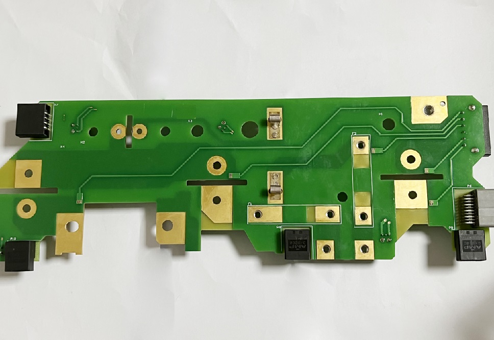
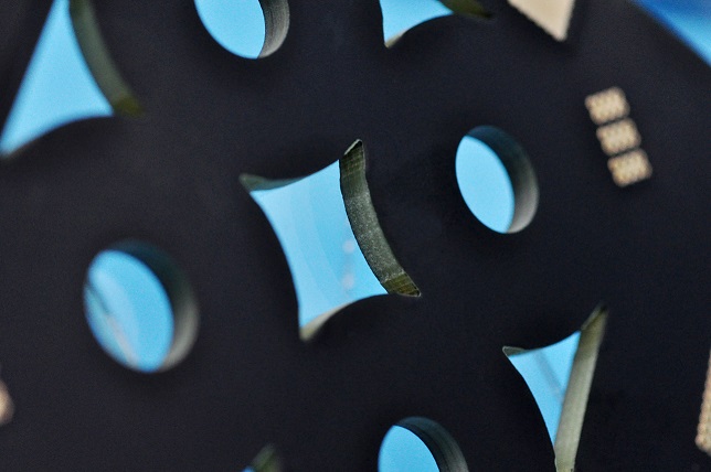
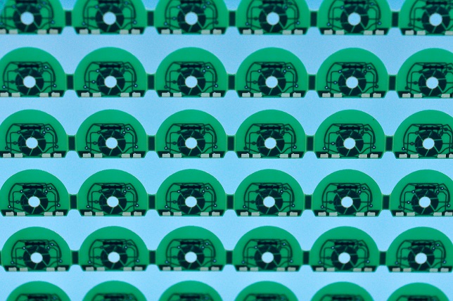
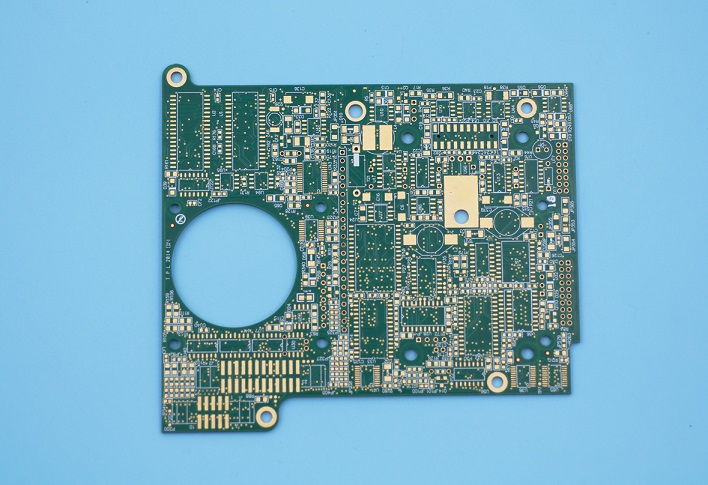
It’s essential to ensure that solder joints are made correctly in any electronics construction. Poor and dry soldering cause equipment not to work once. Or there is a possibility that the solder joint could fail. In this blog, we will introduce why dry soldering occurs and how to solve it.
What is Meant by Dry Soldering?
Dry soldering refers to a poor solder joint that lacks proper electrical connectivity on a PCB assembly product. This issue occurs when the solder does not properly melt and bond to the components, leading to weak connections. These joints are often brittle and prone to failure, which can result in intermittent or complete loss of electrical connectivity.
Why Dry Solder Joint Causes?
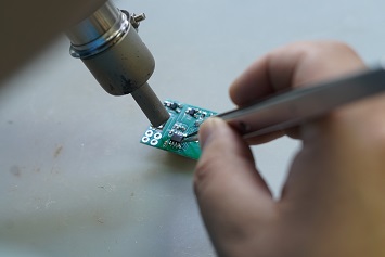
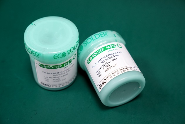
Dry solder joints occur due to several reasons, each impacting the quality of the solder connection. First of all, the solder paste reflow process is only a small area, which is easier to harden than the solder paste in the solder paste can. At this time, the solder paste will not melt, and the flux cannot cover the solder joint, resulting in poor welding of the solder joint. Meanwhile, the solder paste is easier to heat transfer, and the high temperature actually makes the solder paste not easy to melt, so we can slightly adjust the reflow welding temperature curve to solve the problem, or welding in a nitrogen environment is basically a good way to solve this problem.
Secondly, the solder paste does not melt because its own composition contains a very volatile flux, which is also the reason why the solder paste is easy to harden. Among them, the flux with the largest content of solder paste is rosin, rosin contains a lot of rosin acid, rosin acid is easy to lose activity at too high temperature. Therefore, the temperature of the welding process should be controlled to ensure that the temperature is about 200 ° C, which is not suitable for too high or too low. At the same time, the quality of thixotropic agent will also lead to the solder paste is easy to dry, the quality of thixotropic agent is not good will affect the viscosity of the solder paste, the viscosity of the solder paste is easy to dry. Therefore, the choice of high-quality solder paste can fundamentally solve the problem that the solder paste is easy to harden.
In addition, the use of solder paste scene, humidity, temperature and other external factors will also affect the solder paste in the use of hard non-melting phenomenon. So these external factors should be paid attention to. I hope these solutions can solve your problems.
How Do You Fix Dry Solder?
Solder paste is one of the very important materials in the electronics industry, and it has an important impact on the production quality of the entire component. Here are some tips that can help to fix the dry solder paste.
1.Add flux
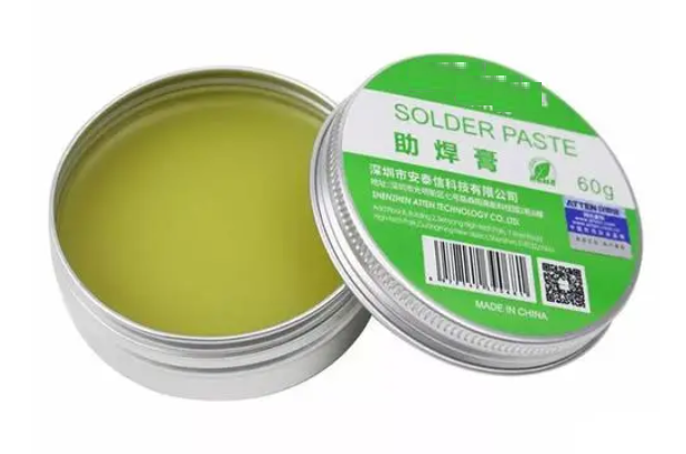
Usually, if the solder paste is too dry, you can try to add some water to the right amount of flux, stir well and add it to the solder paste. This can play a certain role in alleviating drying and improve the fluidity of the solder paste.
2. Take some measurements during management
a. Keep the ambient temperature moderate during storage;
b. Stir well before use;
c. Cover the solder paste in time after welding to avoid exposure to the air.
3. Replace it with new one
If the solder paste becomes too dry, adding flux is difficult to restore its original properties, it is recommended to replace the solder paste to avoid affecting the quality of the components.
Therefore, we need to regularly maintain and manage the solder paste to ensure that its quality meets the standard requirements.
What Does a Dry Solder Look Like?
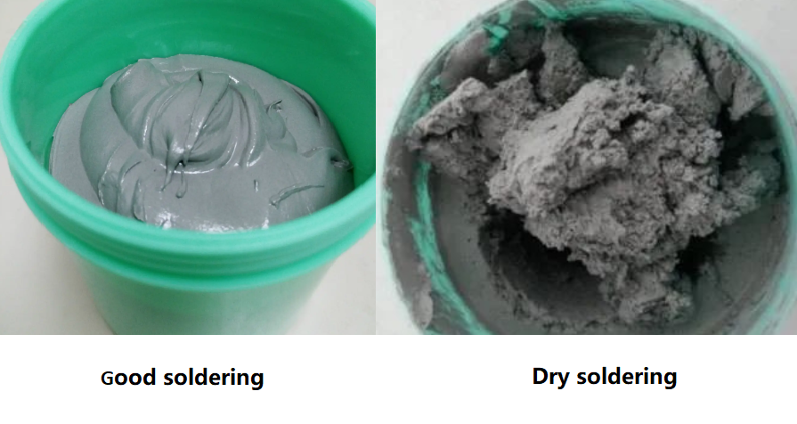
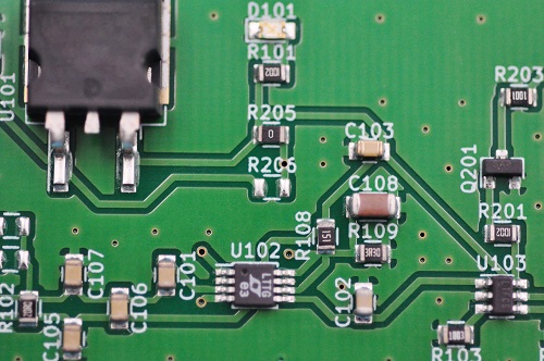
Recognizing a dry solder joint is crucial for proper diagnosis and repair. Unlike a good solder joint, which is shiny and smooth, a dry joint looks matte and rough. The joint might have visible cracks or look brittle. It might not be fully bonded to the component lead or the PCB pad. Identifying these visual cues can help in quickly addressing the issue.
How Do You Prevent Dry Solder?
Preventing dry solder joints is key to maintaining the reliability of your electronic projects. You can try to use these tips to prevent your solder paste become dry.
Proper heating
Clean surfaces
Use quality solder
Steady hand
Maintain equipment
Fast usage and storage
If you want to know more about solutions of dry solder paste, you can read our another post, How to Solve Dry Solder Paste.
How to Tell If Solder is Bad?
Bad solder can lead to dry joints and other issues. So, how can we identify if my solder paste is bad? May you can follow these points. If everything matches up, there’s no doubt that your solder paste is broken.
Appearance of solder joints
Bad solder joints often appear dull or matte instead of shiny and smooth. They may also show cracks or a brittle texture, indicating poor bonding or excessive heating. These visual signs suggest that the solder did not properly melt or flow.
Solder flow and coverage
If the solder does not adequately cover the component leads or PCB pads, or if it spreads unevenly, it is likely bad. Proper soldering should result in a well-formed, consistent fillet around the leads, ensuring reliable electrical connections.
Difficulty in melting
Solder that requires unusually high temperatures or takes a long time to melt may be old or contaminated. Proper solder should melt easily at the recommended temperature and flow smoothly to create a solid joint.
Contamination indicators
Oxidized or tarnished solder indicates contamination and can affect its performance. Excessive residue or debris also points to poor quality, affecting how well the solder adheres and flows.
EBest Circuit (Best Technology) is a one-stop PCB manufacture and PCBA service provider, our SMT factory is equipped with more than 6 assembly lines. Meanwhile, we have automatic SPI machine and solder paste printing machine, with good management system, we can ensure the good quality of solder paste. In addition, there are many advanced equipment in our workshop, including online dual AOI, X-ray, Nitrogen reflow oven, dry-ice cleaning machine, and so on.
Trust us, we are the one of most reliable PCBA manufacturer in China and Vietnam. Contact us for more.
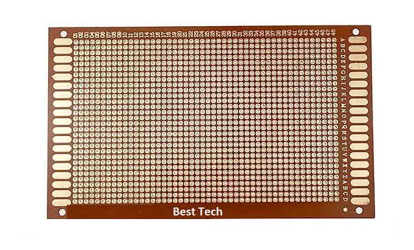
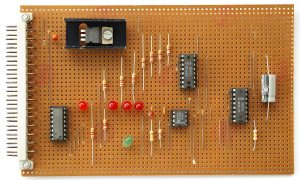
A zero PCB, also known as a prototype PCB or breadboard, is a type of circuit board used for building and testing prototypes. Unlike traditional PCBs, which have pre-defined paths for electric connections, zero PCBs offer a grid of holes. This grid allows for custom circuit designs using wires and components. Engineers and hobbyists use zero PCBs to experiment and develop new electronic circuits without committing to a specific design.
What is a zero PCB?
Zero PCBs are particularly helpful in testing circuit designs for any shortcomings. They provide a cost-efficient way to evaluate the circuitry before committing to a final solution. The term ‘zero’ in this context signifies a fundamental distinction. It implies that there are no predefined connections, layouts, or functions on the PCB.
Generally, there is no solder mask and silkscreen on the zero board. The primary purpose of a zero PCB is to offer a blank canvas for users to create and test custom circuits. As a result, they are intentionally kept simple in structure to allow for maximum customization. Users are free to design and solder their circuits and components directly onto the board without the constraints of a predefined layout or solder mask.
What is the use of a zero board?
Zero boards serve a variety of purposes in the electronics industry. They are particularly useful for prototyping and testing new circuit designs. Here are some common uses:
Prototyping
Educational purposes
Quick fixes
Small-scale production
Zero PCBs have a layer of copper traces or pads on the substrate. These copper elements provide the conductive pathways for soldering electronic components and forming connections. However, the copper traces on zero PCBs are usually unconnected, meaning there is no predefined circuit layout. You can build a circuit on them by inserting components into the holes and then connecting them with wires.
What is the cost of a zero PCB board?
The cost of zero PCB boards varies based on size, material, and supplier. Generally, they are quite cost-effective, so that both professional engineers and hobbyists can afford it. Prices can range from a few cents for small boards to several dollars for larger or more specialized versions. Bulk purchasing often reduces the cost per unit. Additionally, different materials, such as fiberglass or phenolic, can affect the price.
What size is a zero PCB board?
Zero PCB boards come in various sizes to accommodate different project needs. Common sizes include:
Small: Typically around 5×7 cm, ideal for simple projects.
Medium: Sizes like 10×15 cm offer more space for complex circuits.
Large: Boards as large as 30×30 cm are available for extensive projects.
The grid pattern usually remains consistent, with a standard pitch of 2.54 mm (0.1 inches) between holes, regardless of the board’s overall size.
What is a bare board?
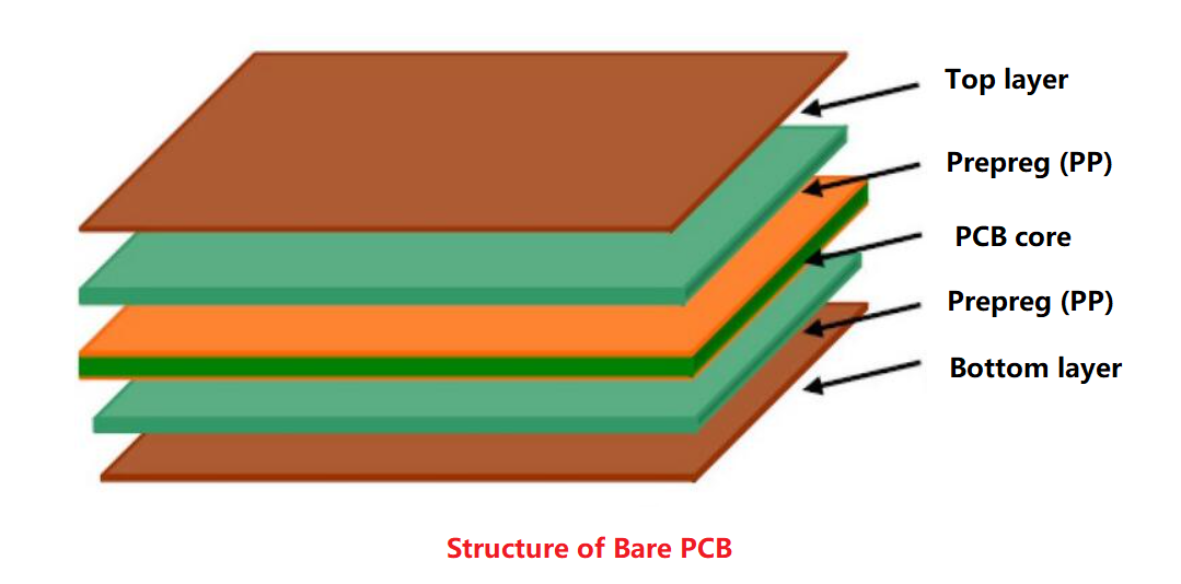
A bare board, also known as a blank PCB, is a printed circuit board that has not yet been populated with any electronic components. It is essentially the foundation of a PCB, consisting only of the substrate material (such as fiberglass) and the copper traces that form the circuit pathways. A bare board typically include base core, prepreg and copper trace layer.
Features of a bare board
Substrate material
The base material of a bare board is usually fiberglass, FR4, or other insulating materials that provide mechanical support.
Copper traces
These are the conductive pathways etched onto the substrate. They form the circuit’s electrical connections but are not yet connected to any components.
Pads and holes
Bare boards include pads (flat areas of copper for soldering components) and drilled holes for through-hole components.
Pre-defined layout
The copper traces and pads are arranged according to a specific design, determined during the PCB design process.
No components
A bare board does not have any electronic components soldered onto it yet. It is essentially a “blank slate” ready to be populated.
Coated solder mask and silkscreen
Most bare boards have a solder mask, a protective layer that prevents solder from bridging between conductive areas, and a silkscreen, which provides component labels and other information.
If you are looking for a reliable supplier for your PCB needs, consider companies like EBest Circuit (Best Technology), who is known for their quality and customer service. EBest Circuit (Best Technology) offers a range of options to support your electronic projects from prototyping to production. Contact us right now to get your quotation.
Metal core printed circiut boards are used where a large of heat are generated in the circuit, and the heat needs to be dissipated quickly to avoid overheat. These boards offer good thermal conductivity and dimensional stability. The aluminum core can reduce the overall weight of your board.
What is Metal Core Printed Circuit Board?
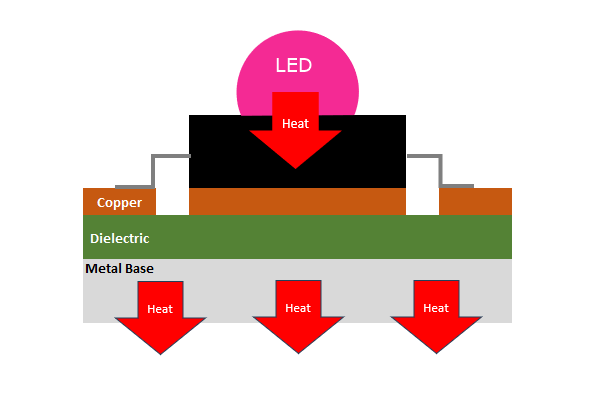
A metal core printed circuit board (MCPCB) is a type of PCB that incorporates a metal core, usually aluminum or copper, as its base material. This core helps to enhance the board’s thermal management capabilities. Unlike traditional PCBs made of fiberglass (FR4), MCPCBs are designed to dissipate heat more effectively, making them ideal for applications where heat dissipation is crucial.
MCPCBs are also referred to as insulated metallic substrate (IMS), or insulated metal PCBs (IMPCB), thermal-clad PCBs. A typical metal core PCB is made of thermal insulating layer (dielectric layer), metal base and copper foil.
The basic constructure of a metal core circuit board includes:
Silkscreen
Solder mask (S/M)
Circuit layer (copper foil layer)
Dielectric layer
Metal core base
What are Metal Core PCBs Used For?
Metal core PCBs are popular because of its good thermal management. It utilizes in various applications that demand efficient heat dissipation and high thermal performance. Here are some common applications that metal core printed circuit board will be used in.
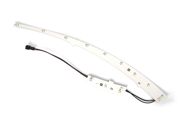
LED lighting
MCPCBs are widely used in LED lighting systems due to their excellent thermal management properties. LEDs generate a significant amount of heat, and metal core PCBs help to dissipate this heat effectively, ensuring longer lifespan and consistent performance of the LEDs.
Power supplies
High-power supply units benefit from MCPCBs as they can handle the heat generated by power components. This helps in maintaining the stability and efficiency of the power supply over time.
Automotive electronics
In the automotive industry, MCPCBs are used in various electronic control units (ECUs), lighting systems, and other high-power applications. The robust nature of MCPCBs makes them suitable for the harsh conditions experienced in automotive environments.
Industrial equipment
Industrial machinery and equipment that operate under high temperatures or require high power output use MCPCBs for their thermal management capabilities. This ensures the reliability and longevity of the equipment.
Telecommunications
Telecommunications equipment, such as base stations and routers, use MCPCBs to manage the heat generated by high-speed and high-frequency operations, ensuring uninterrupted performance and reliability.
Consumer electronics
High-performance consumer electronics, including laptops, smartphones, and gaming consoles. They install with MCPCBs to manage heat and improve device performance and lifespan.
What are the Advantages of Metal Core PCB?
Metal core PCBs are preferred for several reasons, primarily revolving around their superior heat dissipation capabilities and mechanical strength. Here are some main advantages of metal core PCBs.
Superior thermal management
Mechanical strength
Compact design
Enhanced performance
Improved reliability
Higher recyclability
Cost Efficiency
Dimension stability
Size reduction
Longer lifetime
What Metal is Used in PCBs?
The choice of metal in PCBs significantly affects their thermal and mechanical properties. The most commonly used metals in MCPCBs are aluminum and copper. Here’s a closer look at these materials:
Aluminum
Thermal Conductivity: Aluminum has a thermal conductivity of approximately 1.0 to 2.0 W/mK, making it an excellent material for heat dissipation.
Cost-Effective: Aluminum is relatively inexpensive compared to other metals, making it a cost-effective choice for many applications.
Lightweight: Aluminum is lighter than copper, which can be beneficial in applications where weight is a concern.
Corrosion Resistance: Aluminum naturally forms a protective oxide layer, enhancing its resistance to corrosion.
Copper
Thermal Conductivity: Copper has a higher thermal conductivity than aluminum, ranging from 3.0 to 5.0 W/mK, providing superior heat dissipation.
Electrical Conductivity: Copper is also an excellent conductor of electricity, which can improve the electrical performance of the PCB.
Durability: Copper is more durable and resistant to wear and tear compared to aluminum, making it suitable for more demanding applications.
Higher Cost: Copper is more expensive than aluminum, which can increase the cost of the PCB but is justified in applications requiring superior performance.
Other Metals
In some specialized applications, other metals like stainless steel or alloys might be used, but these are less common due to their specific properties and higher costs.
What is the difference between FR4 PCB and Aluminum PCB?
Aluminum PCB is a material based on aluminum base material, coated with an insulating layer and other conductive layers on the aluminum base material. FR4 is a glass fiber reinforced laminate, made of multi-layer fiber cloth and resin composite. In the following, we will introduce the difference between aluminum substrate and FR4 in terms of thermal conductivity, mechanical strength, manufacturing difficulty, application range and thermal expansion coefficient.
1. Aluminum substrate has good heat dissipation, and its thermal conductivity is about 10 times that of FR4.
2. The mechanical strength and toughness of the aluminum substrate are better than FR4, which is suitable for installing large components and making large-area pcb boards.
3. The production of aluminum substrate requires more process steps, and its production process is more complex than FR4, and the production cost is higher than FR4.
4. The aluminum substrate is suitable for high-power electronic products such as LED lighting, power supplies, inverters and solar inverters, and FR4 is suitable for low-power electronic products such as televisions, telephones and electronic game consoles.
5. The thermal expansion coefficient of aluminum substrate is close to that of copper foil, which is smaller than that of FR4, which is good for ensuring the quality and reliability of the circuit board.
Designing a metal core PCB is a complex process that includes several crucial steps. During the design, we should ensure the board meets the thermal, electrical, and mechanical requirements of the application. Below is a detailed guide to the MCPCB design process.
1. Define the Application Requirements
Before starting the design process, it’s essential to clearly define the requirements of your application. This includes understanding the thermal, electrical, and mechanical needs of the project. Determine the maximum operating temperature and the amount of heat that needs to be dissipated, ensuring the MCPCB can handle the thermal load effectively. Specify the electrical characteristics such as current load, voltage levels, and signal integrity requirements to ensure the board can deliver the necessary performance.
2. Select the Core Material
As mentioned above, there are two common metal materials used in this industry: aluminum alloy and copper core. They have unique characteristics and properties when used in device. So. choosing the appropriate metal core material is crucial for the performance of your electronic device. This table provides a side-by-side comparison of aluminum alloy and copper core materials, helping to choose the appropriate material when designing MCPCBs.
Property
Aluminum
Copper
Thermal Conductivity
1.0 – 2.0 W/mK
3.0 – 5.0 W/mK
Electrical Conductivity
Lower than Copper
High
Weight
Light
Heavy
Cost
Lower
High
Mechanical Strength
Good
Excellent
Corrosion Resistance
Natural Protective Oxide Layer
Requires Additional Protection
Thermal Expansion Coefficient
Higher
Lower
Machinability
Good
More Difficult
Environmental Impact
Recyclable
Recyclable
Application Areas
LED Lighting, Consumer Electronics, High-Performance
Electronics, Industrial Equipment
3. Determine the Layer Stack-Up
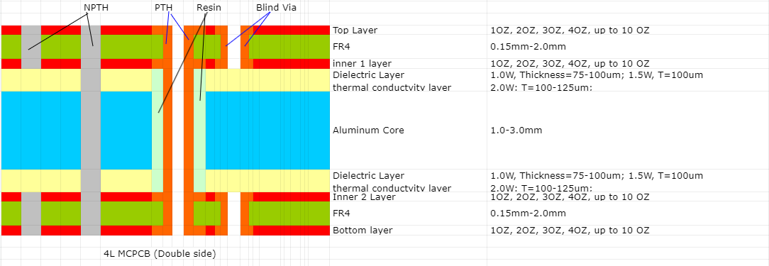
The layer stack-up defines the arrangement of the different layers in the PCB. A typical MCPCB stack-up includes:
Top Copper Layer: The conductive layer where components are mounted.
Dielectric Layer: An insulating layer that separates the copper layer from the metal core. It has good thermal conductivity to transfer heat from the components to the metal core.
Metal Core: The central layer made of aluminum or copper, which acts as a heat spreader.
Bottom Copper Layer (optional): Used in double-sided MCPCBs for additional routing of traces.
4. Design the Circuit Layout
The circuit layout includes placing components and routing traces on the PCB. Key considerations include strategically placing heat-generating components to ensure efficient heat dissipation and keeping sensitive components away from high-heat areas. Trace routing should minimize electrical interference and maintain signal integrity, using wider traces for high-current paths to reduce resistance and heat generation. Implementing thermal vias enhances heat transfer from the top copper layer to the metal core by using plated through holes that connect the copper layer to the metal core, facilitating better heat dissipation.
5. Design for Manufacturability (DFM)
Ensuring that your design can be efficiently manufactured is critical. Maintain adequate clearances between traces, pads, and other features to meet MCPCB manufacturing capabilities and avoid short circuits. Use standard drill sizes to reduce manufacturing complexity and cost. Apply a solder mask to prevent solder bridges and protect the copper traces from oxidation. Use clear and legible silkscreen markings for component identification and assembly instructions. You can communicate with your supplier and ask for a capability chart, so that can save much time on design phase.
6. Prototype and Test
Once the design is validated, create a prototype of the MCPCB and conduct thorough testing. Measure the actual thermal performance under operational conditions to verify the simulation results. Test the functionality of the PCB in the intended application environment to ensure it meets all performance requirements. Conduct reliability tests such as thermal cycling, vibration testing, and humidity testing to assess the durability of the MCPCB.
EBest Circuit (Best Technology) – A Leading MCPCB Manufacturer in Asia
With 18+ years of experience in the PCB industry, EBest Circuit (Best Technology) has a deep understanding of the complexities involved in MCPCB production. Our team of experts is adept at designing and manufacturing MCPCBs that deliver optimal performance. EBest Circuit (Best Technology) offers customized turn-key solutions tailored to the specific needs of our clients. Whether it’s a unique design requirement or a specific material preference, we provide flexible options to meet diverse demands.
Contact EBest Circuit (Best Technology), get your quote right now to make your own metal core circuit boards!
Hey there! If you’re curious about circuit card assembly (CCAs) and what makes them tick, you’ve come to the right place. CCAs are the unsung heroes behind many of the electronic devices we use every day. Let’s dive into what they are, their essential parts, how they’re made, and why they’re so important.
What is a circuit card assembly?
Circuit card assembly or CCA is the process of producing printed circuit boards. In essence, it is the same as PCBA (PCB assembly), just in different name. CCA is a manufacturing technology that converts raw materials into printed circuit boards. It is used in many industries, including the military and aerospace sectors. This type of manufacturing requires skilled professionals to lay out the design and then assemble it. If you are planning to buy a batch of circuit card components, here are some things you should know about CCA.
A circuit card is a thin, flat dielectric material on which conductive paths or traces are etched. These paths connect various electronic components. They are also used to connect components to sockets on printed circuit boards. Circuit card assy is the process of manufacturing circuit card components. The process involves adding electronic components to the substrate.
Key components of a circuit card assembly (CCA)
Circuit card assembly have several key components to make the circuit function properly. These can be divided into three basic components.
Printed Circuit Board (PCB)
Electronic component
Solder paste
Printed Circuit Board (PCB)
This is the backbone of the CCA. The printed circuit board provides the structural foundation on which all other components are mounted. A PCB is typically made of a flat, insulating material such as FR4 fiberglass, which is layered with conductive tracks made of copper. These tracks form the circuit pathways that connect various electronic components. The PCB board can be single-sided, with components and conductive tracks on one side only, or double-sided, with tracks and components on both sides. For more complex applications, multi-layer PCBs are used, which consist of multiple layers of insulating material and conductive pathways stacked together. These printed circuit boards are essential in ensuring that electrical signals are routed efficiently and reliably across the assembly.
Electronic Components
These include resistors, capacitors, integrated circuits, transistors, and more passive and positive components. Each part plays a specific role in the circuit, like pieces of a puzzle fitting together to make a complete picture. Resistors control the flow of electrical current, capacitors store and release energy, integrated circuits (ICs) perform various functions like processing and memory storage, and transistors act as switches or amplifiers. These components are carefully placed on the PCB in positions that allow them to connect and interact as designed.
Solder paste
Solder paste is like the glue that holds everything together, but it’s electrically conductive. It’s used to attach the electronic components to the PCB, so that they can stay put and work properly. Soldering creates a strong, conductive bond between the component leads and the PCB’s copper tracks. There are different types of soldering, such as lead-based and lead-free solders, each with its specific properties and applications. The soldering process can be done manually or using automated printing machines, depending on the complexity and volume of the assembly. Please noticed that solder paste should used in a very short time, otherwise, it will become dry solder paste.
What is the Difference Between a PCB and a CCA?
You might wonder, what’s the difference between a PCB and a CCA? Well, here’s a quick rundown:
Aspect
PCB (Printed Circuit Board)
CCA (Circuit Card Assembly)
Definition
A blank board with conductive pathways
A PCB populated with electronic components
Components
No electronic components
Includes electronic components like resistors, capacitors, ICs
Functionality
Serves as the foundation for electronic circuits
A functional electronic circuit ready for use in devices
Manufacturing Steps
Involves design, etching, and printing of conductive paths
Involves PCB manufacturing plus component placement and soldering
Usage Stage
Intermediate stage in manufacturing
Final stage, ready for integration into electronic devices
Complexity
Less complex, involves fewer manufacturing steps
More complex, involves multiple stages of assembly and testing
What is the circuit card assembly manufacturing process?
Making a CCA is a multi-step process:
Design
First, the PCB layout is designed using computer software. It includes numerous steps, like schematic drawing, layout design, SI, PI analysis, DFM. This can ensure the PCB board can fit all the necessary components and function correctly.
Fabrication
The PCB is then fabricated, which involves creating the physical board with layers of insulating and conductive materials. This is where the board gets its pathways. In this step, proceed strict quality control process to make sure the bare boards are qualified.
Component Placement
Next, printing solder paste and preparing components, then place them onto the PCB board according to the BOM file (bill of material). After setting up the pick and place machine, automated machines can precisely position each component based on the design.
Soldering
The components are soldered to the PCB. This can be done using methods like wave soldering or reflow soldering to ensure everything is securely attached and electrically connected. You must know, different products require different parameters, please make sure all the parameters like temperatures, time are suitable.
Inspection and Testing
The assembled CCA goes through rigorous inspection and testing to ensure it works as intended. This includes visual inspections, automated optical inspections (AOI), in-circuit testing (ICT), aging testing and functional testing.
Final Assembly
If the CCA passes all tests, it moves on to final assembly, where it’s integrated into the larger electronic system or device. That is we say the box building assembly.
What are the types of circuit card assembly?
CCAs can be divided into various types according to the different manufacturing technology.
Through-Hole Technology (THT) Assembly
Here, components have leads or pins inserted into holes drilled through the PCB and soldered on the other side. This method provides strong mechanical bonds, making it great for components that experience mechanical stress. It’s often used in aerospace, military, and industrial equipment.
Surface Mount Technology (SMT) Assembly
In SMT, components are mounted directly onto the PCB surface using solder paste. No drilling required, which allows for higher component density and smaller PCBs. This method is commonly used in consumer electronics, telecommunications, and automotive industries.
Box Building Assembly
Box building assembly involves the complete assembly of electronic systems, including CCAs, into enclosures or boxes. This process includes not only the assembly of the PCB but also the integration of cables, connectors, and other components into a final product. Box building is ideal for producing complete electronic devices ready for end-use.
Advanced materials for CCAs
Advanced materials help CCAs perform better and last longer:
High temperature laminate like FR4 or polyimide. These materials can handle extreme conditions without breaking down. FR-4 is popular for its excellent thermal and mechanical properties, while polyimide is great for high-temperature stability.
Flexible Substrates (e.g., Kapton, PET)
Kapton and PET are the most common flexible substrate. These materials allow CCAs to bend and flex. Kapton, a type of polyimide, is known for its high thermal resistance and flexibility, making it perfect for wearable electronics and medical devices. PET (polyethylene terephthalate) is another flexible material with good electrical insulation properties.
Advanced Solder Compounds
SAC305 (a lead-free alloy of tin, silver, and copper) is favored for its mechanical and thermal properties. Whatever you want to mount a ceramic PCB or the flexible PCB, it is the best choice. Sn63Pb37, a traditional tin-lead solder, is still used for its ease of use and excellent performance.
Reliable circuit card assembly manufacturers
Choosing the right manufacturer for your CCAs is key to getting quality products. PCBonline and EBest Circuit (Best Technology) are go-to-choice reliable circuit card assembly manufacturers. Both of them has advanced pick and place machine, full-auto SPI, AOI equipment, ensuring a good quality.
As a leading manufacturer in the circuit card assembly, EBest Circuit (Best Technology) prides full turn-key service, ranging from the PCB design, PCB fabricating, electronic component sourcing, circuit card assembly and box build assembly. We handle complex and high-volume orders efficiently, ensuring timely and fast delivery without sacrificing quality. In 2023 alone, we completed over 5000 high-complexity projects with a client satisfaction rate of over 98%.
It is crucial for anyone to fullly understand the circuit card assembly in the electronics industry. From their basic components and manufacturing process to the advanced materials used, CCAs are the backbone of modern electronic devices.
In our daily life, the electronics has been gradually infiltrated our lives. Between them, the PCB board plays an important role in it, and we must say, PCB is the foundational element of electronics. From the simplest gadgets to the most complex machinery, PCBs play a crucial role.
What is a PCB Board?
A printed circuit board (PCB) is an electronic that uses metal conductors to create electrical connections between components. Generally, a PCB is a flat, laminated composite made of non-conductive substrate materials with conductive pathways etched or printed onto it. These pathways, also known as traces, enable the electronic components mounted on the board to communicate with each other.
PCBs are designed to support and electrically connect various components such as resistors, capacitors, diodes, and integrated circuits. The intricate network of copper tracks forms circuits that dictate the device’s functionality. PCBs can range from simple single-sided boards used in basic electronics to complex multi-layered structures found in advanced applications.
Common PCB Structure
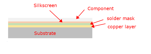
A PCB’s structure is composed of several key layers, each serving a distinct purpose. Here is a detailed breakdown of these layers:
Substrate (Base Material)
The substrate, usually made of fiberglass (FR4), provides the board with its rigidity and thickness. It is the foundational layer upon which all other materials are built.
Copper Layer
This conductive layer is typically made of copper foil. For single-sided PCBs, the copper layer is only on one side of the substrate, whereas double-sided and multi-layer PCBs have copper layers on both sides or between multiple layers of substrate.
Solder Mask
The solder mask is a protective layer applied over the copper traces to prevent oxidation and accidental short-circuiting. It insulates the copper traces and leaves the component pads exposed for soldering. The green color commonly associated with PCBs comes from this layer, though it can also be found in other colors like red, blue, black, and white.
Silkscreen
The silkscreen layer is used to add labels, symbols, logos, and other markings to the PCB. This layer helps in identifying component locations and orientations during assembly and troubleshooting.
Components and Connectors (PCBA)
Components such as resistors, capacitors, diodes, and integrated circuits are soldered onto the PCB. Connectors allow the PCB to interface with other boards, power supplies, and external devices.
How Many Types of PCB?
Single-Sided PCBs
These are the simplest types of PCBs, with copper on only one side of the board. You’ll find them in basic, low-cost electronics like calculators, radios, and power supplies. They’re easy to design and manufacture, which keeps costs down and makes them great for straightforward applications.
Double-Sided PCBs
These boards have copper layers on both sides, allowing for more complex circuits. They’re common in more sophisticated electronics like amplifiers, power monitoring systems, and HVAC systems. With increased circuit density and flexible design options, they can handle more complex tasks.
Multi-Layer PCBs
When you need to pack in a lot of circuits, multi-layer PCBs are the way to go. They consist of three or more layers of copper, separated by insulating layers. You’ll see these in high-tech devices like computers, servers, medical equipment, and aerospace electronics. They offer high circuit density, reduced size and weight, and better signal integrity.
Rigid PCBs
Made from solid, inflexible materials like fiberglass, rigid PCBs keep their shape and provide strong support for components. They’re durable and used in everything from simple toys to complex industrial equipment.
Flexible PCBs
These are made from flexible plastic materials like polyimide, allowing them to bend and flex. Perfect for wearable electronics, flexible displays, and compact devices where space is tight. They’re lightweight, can fit into small, irregular spaces, and can handle being bent repeatedly.
Rigid-Flex PCBs
Combining the best of both rigid and flexible PCBs, these are great for devices that need both stability and flexibility, like smartphones, cameras, and medical devices. They save space, reduce the need for connectors and interconnections, and improve reliability.
High-Frequency PCBs
Designed to operate at frequencies above 1 GHz, these are used in communication systems, microwave technology, and high-speed devices. They provide low signal loss and high performance, making them crucial for advanced communication technologies.
Ceramic PCBs
Using ceramic as the substrate material, these PCBs offer excellent thermal conductivity and stability. They’re perfect for high-power applications and environments with extreme temperatures, like LED lighting, power electronics, and aerospace systems. Ceramic PCBs ensure reliable performance in harsh conditions.
Metal Core PCBs
Featuring a metal core, usually aluminum or copper, these PCBs improve heat dissipation. They’re used in high-power applications where efficient thermal management is crucial, such as LED lighting, power supplies, and automotive electronics.
Special PCBs
Bus Bar PCBs
These integrate bus bars for high-current applications, ensuring efficient power distribution and minimal voltage drop. They’re used in heavy-duty power supplies, electric vehicles, and industrial machinery. Bus bar PCBs provide robust and reliable connections for high-power systems.
Heavy Copper PCBs
With thicker copper layers, typically 3 ounces per square foot or more, these PCBs can handle higher currents and enhance thermal management. They’re used in power distribution, automotive, and industrial applications where durability and performance are critical. Heavy copper PCBs ensure reliable operation under high-stress conditions.
HDI (High-Density Interconnect) PCBs
These feature finer lines and spaces, smaller vias, and higher connection pad density. They’re used in advanced electronics like smartphones, tablets, and medical devices where space and performance are paramount. HDI PCBs enable miniaturization and improved electrical performance.
Extra Thin PCBs
Designed with minimal thickness, these PCBs are perfect for fitting into compact and lightweight devices. You’ll find them in flexible displays, wearables, and miniaturized electronic gadgets. Extra thin PCBs allow for innovative design solutions and space-saving configurations.
RF (Radio Frequency) PCBs
Optimized for high-frequency signals, these are used in communication devices, antennas, and microwave applications. They’re designed to minimize signal loss and interference, ensuring optimal performance in wireless communication systems.
High Tg PCBs
These have a high glass transition temperature, making them suitable for high-temperature environments. Used in automotive, aerospace, and industrial applications, high Tg PCBs maintain structural integrity and performance at elevated temperatures.
Impedance Control PCBs
These are designed to maintain consistent impedance for high-speed signal transmission. They’re used in communication devices, high-speed digital circuits, and advanced computing systems. Impedance control PCBs ensure signal integrity and reduce signal loss and reflection.
Why Are PCB Boards So Expensive?
Material Quality
High-grade materials like FR4 (fiberglass), ceramics, and high-quality copper foil are used to ensure durability and performance. These materials are essential for withstanding environmental stress and ensuring reliable operation, but they are expensive. For example, ceramic substrates can cost up to 10 times more than standard FR4 materials due to their superior thermal conductivity and electrical properties.
Complexity of Design
Multi-layer PCBs and advanced designs such as HDI (High-Density Interconnect) boards require complex manufacturing processes. The process involves precise alignment of layers and sophisticated techniques like laser drilling for micro-vias. The added complexity increases the production costs significantly. For instance, a standard 4-layer PCB might cost $50 per square meter, while a 12-layer HDI PCB could cost over $200 per square meter.
Precision and Technology
Manufacturing high-precision PCBs involves advanced machinery for etching, drilling, and plating. This machinery requires significant investment, and the skilled labor needed to operate it adds to the cost. The precision required in the production process ensures that the PCBs meet exacting standards, crucial for high-performance applications. A single advanced PCB drilling machine can cost upwards of $500,000.
Volume of Production
Smaller production runs generally have higher costs per unit because the setup and tooling expenses are spread over fewer units. For example, a low-volume production run of 10 PCBs might cost $100 per board, whereas a high-volume run of 10,000 boards might reduce the cost to $10 per board due to economies of scale.
Testing and Quality Assurance
Rigorous testing, including electrical, thermal, and functional tests, ensures that the PCBs meet strict performance standards. This testing process is vital to ensure reliability, especially in critical applications like medical devices and aerospace. Quality assurance processes can add 20-30% to the overall production cost, but they are essential for maintaining high standards.
What is the Difference Between PCBA and PCB Board?
The terms PCB and PCBA are often used interchangeably, but they refer to different stages of the board’s life cycle. The PCB is the bare board itself, with no electronic components attached. It consists of a non-conductive substrate, copper traces, solder mask, and silkscreen. A PCB serves as the foundation for assembling electronic components.
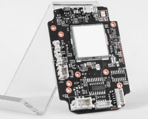
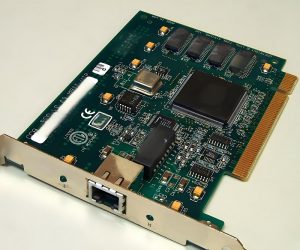
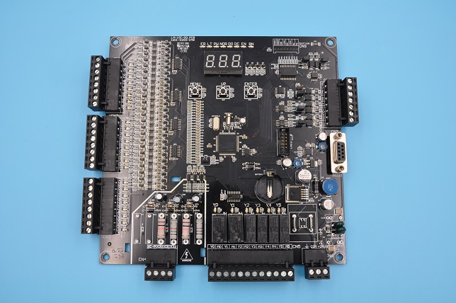
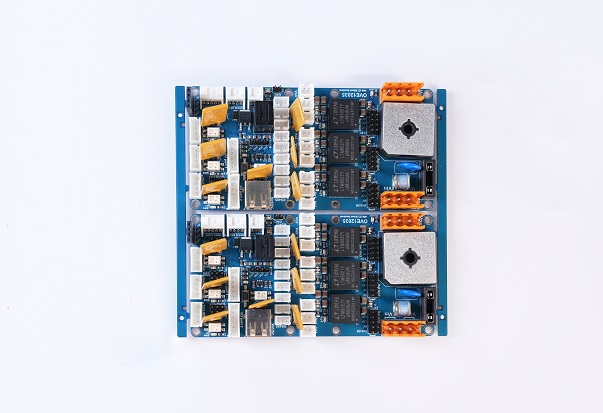
On the other hand, a PCBA (Printed Circuit Board Assembly) is a PCB that has undergone the assembly process, where all necessary electronic components like resistors, capacitors, diodes, and integrated circuits are soldered onto the board. Essentially, a PCBA is a functional circuit board ready for use in electronic devices. The transition from a PCB to a PCBA involves component placement, soldering, and quality testing, transforming the bare board into an operational assembly. Below is a typical PCBA product for your reference.
What is PCB Board Common Use?
PCB boards are existing in everywhere what we live, for example, the global smartphone market, which relies heavily on PCBs, was valued at approximately $520 billion in 2020. Here are some common applications that PCB used in:
Automotive Industry
In the automotive sector, PCBs are used in engine control units, infotainment systems, and advanced driver-assistance systems (ADAS). These applications enhance vehicle performance, safety, and connectivity.
Medical Devices
PCBs are integral to medical devices such as diagnostic equipment, patient monitoring systems, and implantable devices. They ensure precise and reliable operation, which is critical for patient safety and effective treatment.
Industrial Applications
PCBs are used in control systems, machinery, and power distribution units in industrial settings. They provide robust and durable solutions capable of withstanding harsh conditions and continuous operation.
Telecommunications
In telecommunications, PCBs are essential in routers, switches, and communication devices, ensuring efficient and reliable data transmission. As the demand for faster and more reliable communication networks grows, so does the need for high-quality PCBs.
Why Are Circuit Boards Green?
The characteristic green color of most PCBs comes from the solder mask, a protective layer applied over the copper traces to prevent oxidation, short-circuiting, and to protect the board during soldering.
The green color is traditional, largely due to historical reasons and practical benefits. Green solder mask provides a good contrast against the white silkscreen and the shiny copper traces, making it easier for technicians to inspect and identify components during assembly and troubleshooting. Additionally, green solder mask was one of the first colors to be developed and standardized in the industry, leading to its widespread adoption. However, PCBs are not limited to green; they can also be found in other colors such as red, blue, black, and white, depending on the specific requirements and aesthetic preferences of the project. The choice of solder mask color does not affect the performance of the PCB, but green remains popular due to its well-established manufacturing process and visual advantages.
How to Get Started with EBest Circuit (Best Technology)?
Here at EBest Circuit (Best Technology), we are experienced in designing all types of PCBs, including standard rigid PCBs, special PCBs, and irregular PCBs. We can design and develop PCBs according to customer specification and offer suggestions on the right materials for your project.
We provide the full series of PCB manufacturing, from the initial PCB design, PCB layout, to custom PCB fabricate, PCB assembly, box building and so forth. By the way, we have our own factory in Vietnam, that means we can ship out the PCBs directly from Vietnam.
Welcome to contact us when you want to get a quote!
FR4 is a commonly used material in the printed circuit boards (PCBs) manufacturing. If you’re in the electronics field, you’ve likely heard of it. It is the footstone of a circuit board, provides good mechanical strengthen and electrical insulation properties. Today, we will share informational about FR4 material, its types, advantages and alternatives. Keep reading if you are interested in.
What does FR4 stand for?
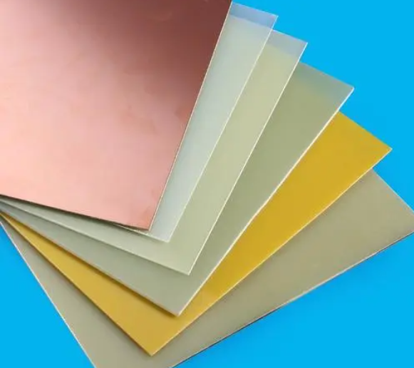
FR4 stands for “Flame Retardant 4”, also called FR-4 Epoxy Glass Cloth by PCB manufacturers. It is not a material name, but a material grade, so there are many types of FR-4 grade materials used in general circuit boards. But most are composites made with so-called Tera-Function epoxy resins plus fillers and glass fibers. FR4 is made from woven glass-reinforced epoxy resin. The typical composition of FR4 includes approximately 60% glass fabric and 40% epoxy resin by weight.
This composite material is known for its high mechanical strength and flame-retardant properties. The “4” in FR4 signifies the level of flame retardancy. It means the material is resistant to catching fire, which is critical in preventing electrical fires in electronic devices.
What are the classifications of FR4 materials?
FR4 materials are classified based on various properties and specifications to cater to different applications and requirements. These classifications help in selecting the right type of FR4 material for specific PCB needs. Here are the primary classifications of FR4 materials:
1. Standard FR4
Standard FR4 is the most commonly used classification. It offers a good balance of electrical insulation, mechanical strength, flame retardancy, and cost-effectiveness. Standard FR4 materials have a glass transition temperature (Tg) typically around 130°C to 140°C. They are suitable for general-purpose PCBs used in consumer electronics, industrial controls, and telecommunications equipment.
2. High Tg FR4
High Tg FR4 materials are designed for applications requiring higher thermal performance. These materials have a higher glass transition temperature, usually above 170°C. High Tg FR4 is used in applications where the PCB is exposed to higher temperatures, such as automotive electronics, aerospace, and high-power devices. The increased Tg provides better stability and performance at elevated temperatures. This is the high Tg FR4 PCB that we made before.
3. Low Dk FR4
Low Dk (Dielectric Constant) FR4 materials are used in high-frequency applications where signal integrity is crucial. So, we called it as “High-frequency FR4”. These materials have a lower dielectric constant, which reduces signal loss and improves signal transmission. Low Dk FR4 is often used in RF and microwave circuits, where maintaining signal integrity is essential.
4. High CTI FR4
High CTI (Comparative Tracking Index) FR4 materials have an improved resistance to electrical tracking. These materials are used in applications where the PCB is exposed to high voltages and harsh environments. High CTI FR4 provides better insulation and reduces the risk of electrical failure due to tracking.
5. Halogen-Free FR4
Halogen-free FR4 materials are designed to meet environmental and safety requirements by eliminating halogens. Which can be harmful if released during PCB manufacturing or disposal. These materials are used in applications where reducing environmental impact is a priority. Halogen-free FR4 offers similar performance to standard FR4 but without the use of halogenated flame retardants.
Benefits of using FR4 as PCB material
Excellent Electrical Insulation
High Mechanical Strength
Flame Retardancy
Moisture Resistance
Cost-Effectiveness
Thermal Stability
Ease of Fabrication
Properties of FR4 material
Property
Parameter
Vertical flexural strength
Normal State: E-1/150, 150±5℃≥340Mpa
Parallel layer impact strength
≥230KJ/m
Insulation resistance after water immersion (d-24/23)
≥5.0×10⁸Ω
Vertical electrical strength
≥14.2MV/m
Parallel layer breakdown
≥40KV
Relative Dielectric Constant (50hz)
≤5.5
Relative Dielectric Constant (1mhz)
≤5.5
Dielectric Loss Factor (50hz)
≤0.04
Dielectric Loss Factor (1mhz)
≤0.04
Water Absorption (D-24/23, 1.6mm Thickness)
≤19mg
Density
1.70-1.90g/cm³
Flammability
FV0
What is the Difference Between IMS and FR4 PCB?
IMS (Insulated Metal Substrate) and FR4 PCBs serve different purposes. IMS PCBs are designed for applications requiring efficient heat dissipation. They have a metal base layer that helps manage heat more effectively than FR4. This makes IMS ideal for high-power applications like LED lighting.
On the other hand, FR4 PCBs are used in general electronic applications due to their balance of performance and cost. While IMS excels in thermal management, FR4 is preferred for its electrical properties and versatility.
What is the Cost of FR4 PCB Per Square Inch?
The cost of an FR4 PCB can vary based on several factors. These include the board’s thickness, the number of layers, and the complexity of the design. On average, the cost per square inch of FR4 PCB ranges from $0.10 to $0.50. However, this is a rough estimate. For a precise quote, it’s best to contact PCB manufacturers with your specific requirements. If you are searching for a PCB supplier, EBest Circuit (Best Technology) is here to waiting for you.
Why is Rogers Better Than FR4 Material?
Rogers material is often considered superior to FR4 in high-frequency applications. Here are some key reasons why Rogers might be chosen over FR4.
Lower Dielectric Loss
Higher Thermal Conductivity
Improved Dimensional Stability
Consistent Dielectric Constant
Superior Performance in High-Frequency Applications
Compliance with Stringent Industry Standards
What Material is Similar to FR4?
Several materials are similar to FR4 and can be used as alternatives. One such material is CEM-1, which is also a composite material made from epoxy and fiberglass. It offers good mechanical strength and electrical properties but is less flame retardant than FR4.
Another alternative is polyimide, known for its excellent thermal stability and flexibility. It is often used in applications requiring high-temperature resistance. However, polyimide is more expensive than FR4. For specific applications, materials like PTFE (Teflon) can also be considered, especially in high-frequency applications.
FAQs
1. Can FR4 be used in high-temperature applications?
FR4 can withstand moderate temperatures, but for high-temperature applications, materials like polyimide are preferred.
2. Is FR4 environmentally friendly?
FR4 is not biodegradable but can be recycled to some extent. Proper disposal and recycling methods should be followed.
3. How does the thickness of FR4 affect PCB performance?
The thickness of FR4 can impact the board’s mechanical strength and thermal dissipation. Thicker boards offer more durability but may also increase the cost.
4. Are there any disadvantages to using FR4?
FR4 has limitations in high-frequency and high-temperature applications. It is also less effective in thermal management compared to materials like IMS.
5. Can FR4 PCBs be used in flexible circuits?
FR4 is rigid and not suitable for flexible circuits. For flexible applications, materials like polyimide are used. But recently, EBest Circuit (Best Technology) developed a new product called “semi-flexible FR4 PCB”, its flex area is made by FR4 material.
Is FR4 RoHS Compliant?
Yes, FR4 is RoHS compliant. This means that it meets the regulations set by the European Union to limit the use of specific hazardous materials found in electrical and electronic products.
What is FR4 Tg?
The glass transition temperature (Tg) of FR4 is a critical property that indicates the temperature at which the material transitions from a hard, glassy state to a soft, rubbery state.
EBest Circuit (Best Technology) excels not only in PCB and assembly manufacturing, but also in offering top-quality PCB design services. Our professional engineering team is ready to support your innovation across various industries, including communications, healthcare, industrial, and consumer electronics. We welcome all the questions or inquiries from you.
If you are familiar with SMT or PCB assembly process, you may know BOM file. It is an important element in the SMT process. Creating BOM is a crucial step in the manufacturing process, especially for PCBs. A BOM serves as a comprehensive list of all the parts, components, and materials needed to build your product. It ensures that everyone involved in the production process is on the same page, reducing the risk of errors and delays. Today, EBest Circuit (Best Technology) would like to introduce BOM and giving you a guide to create a BOM file step by step.
What is a Bill of Materials (BOM)?
A Bill of Materials (BOM) is a detailed list of all the parts, components, and materials needed to manufacture a product. In PCB manufacturing, a BOM outlines every item required to assemble a PCB, including quantities, part numbers, and descriptions. It serves as a guide to ensure that the manufacturing process runs smoothly and that no crucial components are missing.
Types of Bill of Materials
There are several types of BOMs used in different stages of production. Each type serves a specific purpose and provides unique details to streamline processes and ensure accuracy. Here are the primary types of BOMs:
Engineering BOM
This type of BOM is creating during the design phase. It lists all the parts and components designed by the engineering team, including specifications and relationships as intended in the final product. And of course, it mainly used by design engineers to communicate the product structure and details to manufacturing teams.
Manufacturing BOM (Formal)
It is a formal BOM files that used in the assembly phase. Different with engineering BOM, it includes additional details necessary for manufacturing, such as packaging, handling instructions and assembly details. And some special instructions.
Sales BOM
Sales BOM is used by sales teams and includes information relevant to the sales process, such as pricing and availability. It helps in providing accurate quotes, managing customer expectations, and handling sales orders efficiently.
What Should Include in an Effective Bill of Materials?
An effective BOM should be detailed, accurate, and easy to understand. It should include all the details of components and indicated revisions. As a 18 years expertise in PCBA production, we summarized the key elements that should be included in the BOM.
Component details
It should include all the components and their detailed information, such as names, part numbers (PN), and descriptions for each part.
Quantity (QTY)
The exact quantity of each component required for the product. Accurate quantities can prevent shortages and overstocking.
Foot print
It is the package of each component, helping to ensure the correction of part.
Reference Designators
Unique identifiers that match each component to its specific location on the product layout. These are essential for assembly and troubleshooting.
Manufacturer Information
Manufacturer information, including the manufacturer name of components and manufacturer part number. It helps to ensure correct parts are sourced. And convenient for alternative part sourcing if it is shortage.
Supplier information (Optional)
It means the name of the supplier or distributor. The part number used by the supplier, which may differ from the manufacturer’s part number.
Assembly instructions
Any special notes for assembly such as DNF remark, and version control to track revisions should also be included. Additionally, cost information helps in budgeting, and lifecycle status information helps plan for component availability and avoid discontinued parts.
How to Make a PCB Bill of Materials (BOM)?
Creating a PCB BOM is a systematic process that involves compiling all the necessary information about each component required for the assembly of the PCB. Here’s a detailed guide on how to create a PCB BOM:
Open a Blank Spreadsheet
Use software like Microsoft Excel or Google Sheets to start with a blank spreadsheet. They are common to use, offering flexibility and ease of use for creating and managing BOMs.
Define Columns
Set up your spreadsheet with appropriate column headers. Common headers include:
Part Number
Component Name
Quantity
Reference Designator
Manufacturer
Manufacturer Part Number
Supplier
Supplier Part Number
Description
Package Type
Cost
Notes
Input Data
Enter the required details for each component under the appropriate headers. Please be make sure that all information is accurate and complete. This may involve referencing design files, datasheets, and supplier catalogs. If it is incorrect, then it needs a lot of time to find out and revise the errors, resulting in schedule delay.
Use Formulas
Utilize Excel formulas to automate calculations, such as summing total quantities or calculating costs. This helps in reducing manual errors and saves time.
Format for Clarity
Use cell formatting options to highlight important information and ensure the spreadsheet is easy to read. For example, you can use bold text for column headers, color coding for different component types, and borders to separate sections.
Include Version Control
Add a version control section to your BOM to track revisions and updates. This can be a simple row at the top or bottom of the spreadsheet, indicating the version number, date of revision, and a brief description of changes.
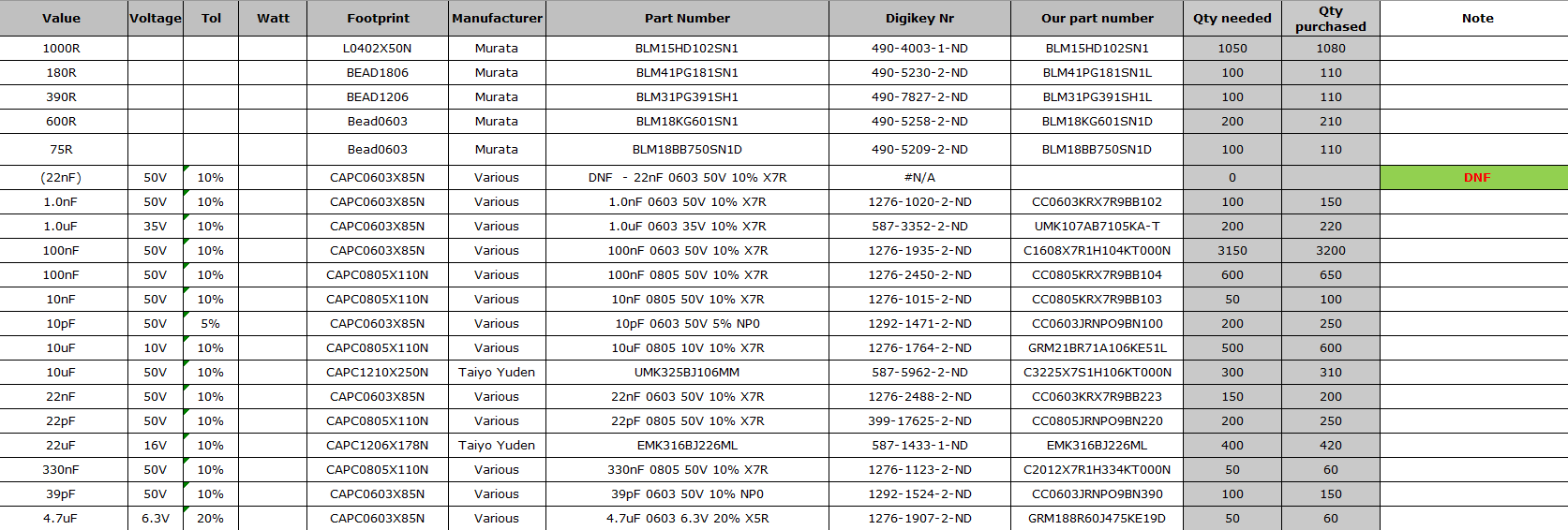
(BOM file reference)
Save and Update
Save your BOM and update it regularly to reflect any changes in the design or component availability. Regular updates ensure that the BOM remains accurate and up-to-date, preventing issues during production.
Review and Verify
Have multiple team members review the BOM for accuracy. Cross-check all component details, quantities, and part numbers against the design files. Verification helps catch errors early and ensures the BOM is reliable.
Communicate with Suppliers:
Maintain open communication with suppliers to confirm component details and availability. This ensures that you can source the correct parts and avoid delays in the production process.
How Can I Optimize My BOM for PCB Assembly?
Sometimes, a simple BOM is not good to process PCB assembly process, and manufacturers may need to spend a lot of time to optimize it, make into convenient for manufacturing. If you are a layman, here are some steps to help you in optimizing your BOM file.
First, it’s a good idea to standardize components where possible. Using standard parts that are readily available from multiple suppliers can simplify procurement and reduce costs. This approach minimizes the risk of shortages and ensures you can get parts quickly and affordably. Also, make sure all entries in your BOM are clear and concise to avoid confusion during assembly. Double-checking part numbers and quantities against design files is crucial to prevent errors that could lead to rework or delays.
Building strong relationships with your suppliers is another key factor. Good communication with suppliers helps ensure reliable component availability and keeps you informed about any changes in lead times or part availability. Regularly updating your BOM to reflect any design changes or component availability issues is essential. Keeping your BOM current and accurate prevents last-minute surprises during assembly.
What Common Mistakes Should I Avoid When Creating a PCB BOM?
Avoiding common mistakes in BOM creation can save time and reduce errors. Here are some pitfalls to watch out for:
Incomplete information – ensure all necessary details are included for each component.
Incorrect quantities – double-check quantities to avoid shortages or excess inventory.
Outdated data – keep the BOM updated with the latest design changes and component information.
Ambiguous descriptions – provide clear and precise descriptions to prevent confusion.
Lack of version information – implement version control to track changes and ensure the correct BOM version is used.
Creating an effective and accurate PCB BOM is essential for smooth manufacturing and assembly. By following best practices and using the right tools, you can ensure your BOM is comprehensive, clear, and up-to-date, ultimately leading to a successful PCB production process.
EBest Circuit (Best Technology) is an expert in SMT and PCB assembly, we have more than 18 years in this industry, that can offer you a best experience of PCBA solution. In our facotry, we have advanced equipment like full auto pick and place machine, online dual AOI, X-ray, 3D SPI, nitride reflow oven and three-proof paint machine. So that we can ensure the fast lead time and high quality of your PCBA products. Reach us to get a instant quote!
In the world of printed circuit boards (PCBs), understanding material properties is crucial. One such property is Tg, or glass transition temperature. For FR4 PCBs, knowing what Tg means can significantly impact design and performance. In this blog, we’ll explore what Tg is, how it’s measured, its importance, and other related questions.
What Does Tg Mean in PCB Manufacturing?
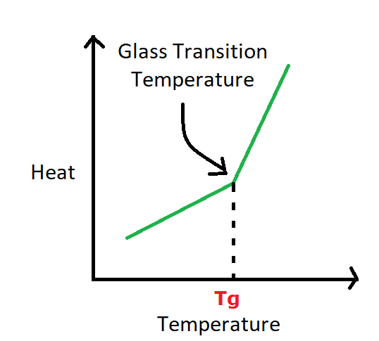
Tg stands for glass transition temperature. It refers to the temperature at which a polymer material, such as the resin in a PCB substrate, transitions from a hard, glassy state to a softer, rubbery state.
For the circuit board, the Tg value reflects the highest temperature it can withstand. When the temperature exceeds Tg values, the molecular structure of the circuit board material will be changed, lead to changes in its physical properties. Such as mechanical strength, size stability, adhesive, water imbibition, thermal expansion, etc. Therefore, the level of TG value of the PCB directly affects the stability and high temperature resistance of the circuit board.
In the high temperature environment, if the TG value of the circuit board is too low, it is easy to cause PCB deformation, fracture, cracking and other problems, affecting the reliability and life of the printed circuit board. If the TG value of the circuit board is too high, the PCB is easy to become hard and brittle, affecting the processability and flexibility of the circuit board.
How is Tg Measured in FR4 Materials?
Accurate measurement of Tg is crucial for ensuring the performance and reliability of FR4 PCBs. Knowing the exact Tg helps in selecting the appropriate material for specific applications, particularly those involving high temperatures and thermal cycling. Using materials with a Tg well above the operating temperature ensures the PCB will maintain its mechanical and electrical properties under expected conditions.
The primary method for measuring Tg in FR4 materials is by differential scanning calorimetry (DSC). It involves heating a small sample of the material at a controlled rate, typically between 10°C to 20°C/min. As the sample heats, the DSC measures the heat flow into the material and records it as a thermogram. The Tg is identified as the temperature where there is a noticeable change in heat capacity, appearing as a step or inflection point on the thermogram. DSC is widely used because it provides precise and reliable Tg measurements.
Additionally, Dynamic Mechanical Analysis (DMA) and Thermomechanical Analysis (TMA) also can be used to measure the Tg value.
Why is Glass Transition Temperature Critical in PCBs?
Glass transition temperature is critical because it affects the thermal and mechanical properties of the PCB. If a PCB operates near or above its Tg, it can experience issues like delamination, warping, and electrical failure. Here are some benefits of Tg.
Thermal stability
One of the main reasons is its role in determining thermal stability. During operation, PCBs are subjected to varying temperatures due to power dissipation from electronic components and environmental conditions. Make sure the Tg of the PCB material is well above the maximum operating temperature, it helps maintain mechanical stability and reliable performance under thermal stress.
Mechanical Strength
The Tg value also affects the mechanical strength and durability of the PCB. Below the Tg, the material is rigid and can withstand mechanical stress without significant deformation. This rigidity is essential for maintaining the structural integrity of the PCB, especially during assembly processes like soldering, where the board is subjected to mechanical and thermal stresses.
Thermal Management
Thermal management is very important to electronics, especially for those miniaturized electronic devices. If the PCB itself has good thermal management, then designers no need to install heatsink or coolers. Materials with higher Tg values exhibit lower coefficients of thermal expansion (CTE), meaning less expansion and contraction with temperature changes.
Application-specific requirements
Different applications have varying thermal and mechanical requirements. High-performance computing, automotive, aerospace, and industrial electronics often operate in environments with high temperatures and thermal cycling. For these applications, using PCB materials with appropriate Tg values is crucial.
What is the Typical Tg Value for Standard FR4 PCBs?
Standard FR4 materials generally have Tg values in the range of 130°C to 140°C. For high-performance applications, materials with higher Tg values are necessary. The table below lists some common high Tg materials used in PCB manufacturing, along with their Tg values and characteristics.
Material
Tg Value (°C)
Characteristics
Applications
ISOLA IS410
180
Excellent thermal and mechanical properties
High-reliability applications
Nanya NP-175
175
High thermal stability, good mechanical strength
Automotive, industrial electronics
Shengyi S1000H
170
Cost-effective, widely used
Consumer electronics, industrial applications
Ventec VT-47
170
High Tg and low CTE
High-density interconnect (HDI) PCBs
Rogers 4350B
280
Extremely high Tg, excellent thermal stability
RF and microwave applications
(Common used high Tg materials)
Can You Explain the Difference Between Tg and Td in PCBs?
Tg and Td (decomposition temperature) are two different thermal properties. Unlike the reversible physical change associated with Tg, decomposition is an irreversible chemical process. At Td, the polymer chains in the material break down, leading to a loss of structural integrity and release of volatile compounds. Key points about Td include:
1. Chemical Stability
Td represents the upper thermal limit of a material’s chemical stability. Exceeding Td results in the breakdown of the polymer structure, rendering the material unsuitable for further use.
2. Material Selection
Knowing the Td helps in selecting materials for high-temperature applications. A material’s Td should be well above the maximum operating temperature to prevent degradation.
3. Safety and Reliability
Operating a PCB above its Td can result in catastrophic failure, including charring, delamination, and loss of electrical performance. The operating temperature remains below Td is critical for safety and reliability.
How Do You Choose the Right Tg Value for Your PCB Design?
Choosing the right Tg value depends on the operating environment and thermal demands of your application. Consider factors such as the maximum operating temperature, the thermal cycling the PCB will undergo, and the mechanical stresses it will face. Consulting with material suppliers and using simulation tools can help make an informed decision. According to our 18 years experience in PCB, we summarized a recommend Tg value for each application. Hope this is useful for you guys.
Consumer electronics
If your PCB will be used in standard consumer electronics, just like smartphones and tablets, a Tg value of around 130°C to 140°C is typically sufficient. These devices generally do not encounter extreme temperatures or thermal cycling.
Automotive applications
Automotive PCBs are always exposed to high temperatures and significant thermal cycling. A Tg value of 170°C or higher is recommended to ensure reliability and performance under the hood. So, Rogers material is good for this kind of PCB.
Aerospace and defense
Applications in aerospace and defense require materials that can withstand extreme temperatures and harsh environments. High Tg materials with values of 180°C or more are often used to meet these stringent requirements.
Industrial Electronics
Industrial environments can vary widely, but generally, high Tg materials are preferred due to the exposure to high temperatures and mechanical stress. A Tg value of at least 150°C to 170°C is advisable.
EBest Circuit (Best Technology) is a well-known PCB and PCBA assembly provider in Asia and Vietnam. We have a large facility for handling low-medium to mass production PCBs, and supporting for various kinds of custom PCBs. Some special PCBs are available here, like bus bar PCB for new energy vehicles, heavy copper PCB for high power and high current PCBs, ceramic PCBs for harsh environments, extra thin PCB, RF PCB, microwaves PCB, IC substrate PCB and so on.
For more information, please do not hesitate to contact us.
Ceramic PCBs are a special breed of printed circuit boards known for their exceptional thermal resistance and durability. These PCBs are used in industries where high performance is critical, such as aerospace, automotive, medical devices, and power electronics. Nowadays, the most common types of ceramic PCB are thick film, DCB, DPC, AMB, HTCC, LTCC and thin film. In this article, we will introduce each of them in details.
Thick Film Ceramic PCB
Thick film technology is a process by using screen printing conductor paste and directly deposit slurry (conductor) on the ceramic substrate. Then sintering it under high temperature to form conductive circuit traces and electrodes, which is suitable for most ceramic substrates.
After the material is sintered at high temperature, a strong adhesion film will be formed on the ceramic circuit board, repeat this step for many times, a multi-layer circuit is generated.
You can print resistor or capacitor on the surface to get a interconnected structure. At EBest Circuit (Best Technology), we can make all the resistors with the same value, or different value for different resistor on the same board.
Thick film ceramic PCB has advantages on the simple manufacturing process, but it has some drawbacks that can’t be ignored:
Limited by the conductive paste and screen size
Line width less than 100um is difficult to achieved
Three-dimensional patterns are not available
Not suitable for fine-trace project
DBC / DCB Ceramic PCB
Direct Bonded Copper (DBC) or Direct Copper Bonded (DCB) ceramic PCBs are known for their excellent thermal conductivity. They are made by bonding a layer of copper directly onto a ceramic substrate, typically aluminum oxide or aluminum nitride. Due to the DBC technology is directly bond copper on the ceramic substrate, it can achieve thicker copper thickness to 300um. So, it is very suitable for high power applications.
The basic chemistry principle is to introduce an appropriate amount of oxygen between copper and ceramics before or during the application process. Copper and oxygen will form Cu-O eutectic liquid under 1065℃~1083℃. This is an important element in the manufacturing. DBC ceramic circuit board uses this eutectic solution to chemically react with the ceramic substrate to form CuAlO2 or CuAl2O4, achieving the combination between substrate and copper foil.
However, it is easy to generate micro-porosity between Al2O3 and Copper during the copper bonded process, and it doesn’t have a good solution by far. That is why the yield of DBC ceramic PCB is not good than DPC.
DPC (Direct Plated Copper Ceramic PCB)
DPC ceramic PCB utilizes direct copper plating technology, deposit copper foil on the alumina oxide (Al2O3) substrate. It is the most commonly used ceramic PCB in recent years. The circuit generated process is: pre-treatment – sputtering – exposure – develop – etch – strip – electroplating.
AMB (Active Metal Brazed Ceramic PCB)
AMB ceramic copper clad plate adopts the active brazing process, and the copper layer bonding force is higher than that of DPC, which is around 18n/mm – 21n/mm. AMB ceramic copper clad plate usually has a high binding force, usually makes thicker copper, between 100um and 800um. The AMB ceramic PCB generally rarely design traces or holes, even if there is a trace is very simple, the spacing is relatively wide.
HTCC (High Temperature Co-fired Ceramic PCB)
HTCC is a relatively early development technology, but due to the high sintering temperature (1300~1600℃), the choice of electrode materials is limited. Meanwhile, its cost is more expensive, these promotes the development of HTCC is relatively slow.
LTCC (Low Temperature Co-fired Ceramic PCB)
Although LTCC reduces the co-firing temperature to about 850 ° C, the disadvantage is that the dimensional accuracy and product strength are not easy to control.
Thin Film Ceramic Circuit Board
The thin film ceramic PCB is to deposit a metal layer directly on the surface of substrate by sputtering process. Through lithography, development, etching and other processes, the metal layer can also be graphed into a circuit pattern. Due to the low deposition speed of sputtering coating (generally less than 1μm/h), thin film substrate surface metal layer thickness is small and can prepare high pattern accuracy (line width/line space less than 10μm).
Common Ceramic Substrates
EBest Circuit (Best Technology) is a leading ceramic PCB manufacturer in Asia, our core members has over 20 years manufacturing experience in ceramic PCB fabricating. “High mixed, low volume, high quality, fast delivery” is our advantages and we always try our best to do that, make ourselves better and better. If you are interested in it, feel free to contact us, we are always online.
With the gradual deepening of electronic technology in various application fields, the highly integrated circuit board has become an inevitable trend. Under this situation, the disadvantage of traditional circuit board FR-4 and CIM-3 in TC (thermal conductivity) has become a drawback to delay the development of electronic technology. Though the metal core PCBs are known for their good thermal management, they hard to meet the fast heat dissipation and miniaturization of the devices at the same time. This is why ceramic PCB stands out.
What is Ceramic PCB?
A ceramic PCB is a type of PCB made from ceramic materials, such as alumina (Al2O3), ALN (aluminum nitride), or Beryllium Oxide (BeO). These materials are prepared by using thermal conductive ceramic powder and organic adhesive under the condition of below 250℃. Ceramic powders are not easy to made, especially for aluminum nitride powder, this is one of reasons that why ALN ceramic PCB is more expensive.
There are some different methods to make ceramic PCBs, commonly in the market are thick film, DBC, DPC and thin film technology. Different types of ceramic circuit boards have its unique characteristics. May you heard about HTCC, LTCC and AMB, they are also the ways to make ceramic PCBs, but there just a few manufacturers can make. Here is a HTCC ceramic PCB that we made.
Why Ceramic PCBs are popular used?
Different from the traditional FR-4 PCB (wave fiber), ceramic PCBs have good high-frequency properties, electrical properties that organic materials can’t achieved. It is a new generation of large-scale integrated circuits and power electronics module ideal packaging materials. The main advantages of ceramic circuit board including:
Higher thermal conductivity
More matched thermal expansion coefficient (CTE)
Lower resistance
Good weldability and can be used in high temperature
Good insulation
Lower high-frequency loss
High density assembly available
No organic ingredients, resistance to cosmic rays, high reliability in aerospace
No oxide layer in copper layer, so it can be used for a long time in a reducing atmosphere
Who is the Best Ceramic PCB Manufacturer?
There are so many PCB manufacturers in the domestic and aboard, but reliable ceramic PCB vendors with good quality and reasonable price are very few. If you are looking for an experienced one, then keep the change. We’re the best option! EBest Circuit (Best Technology) offers ceramic PCBs for our customers more than 100k every year, and we are high mixed from thick film ceramic PCB, DPC ceramic PCB, DBC/DCB ceramic PCB to AMB. Your PCBs need to use in automotives? Don’t worry, we gained IATF16949 and ISO13485 certifications, and all the manufacturing processes are strictly followed by ISO9001 quality control system. We welcome all the questions and inquiries from everyone.
Here is our ceramic PCB manufacturing capability for your reference.
Ceramic PCB Manufacturing Capability
No.
Item
General Parameter
Special Process
1
Substrate
High insulation, chemical corrosion resistance, high-temperature resistance
Al2O3
Glass, quartz, sapphire, 99% , 92% Al2O3 (black)
2
Excellent thermal conductivity, low thermal expansion coefficient, and high-temperature resistance
AIN
3
Insulation performance and high-temperature stability
ZTA
4
High strength, high hardness, high thermal conductivity, and low dielectric loss
This website uses cookies to enhance your experience, remember your preferences, and help us understand how visitors use our site. You can accept all cookies, reject non-essential cookies, or manage your settings.
This website uses cookies to improve your experience while you navigate through the website. Out of these cookies, the cookies that are categorized as necessary are stored on your browser as they are essential for the working of basic functionalities of the website. We also use third-party cookies that help us analyze and understand how you use this website. These cookies will be stored in your browser only with your consent. You also have the option to opt-out of these cookies. But opting out of some of these cookies may have an effect on your browsing experience.
Necessary cookies are absolutely essential for the website to function properly. These cookies ensure basic functionalities and security features of the website, anonymously.
Cookie
Duration
Description
cookielawinfo-checkbox-analytics
11 months
This cookie is set by GDPR Cookie Consent plugin. The cookie is used to store the user consent for the cookies in the category "Analytics".
cookielawinfo-checkbox-functional
11 months
The cookie is set by GDPR cookie consent to record the user consent for the cookies in the category "Functional".
cookielawinfo-checkbox-necessary
11 months
This cookie is set by GDPR Cookie Consent plugin. The cookies is used to store the user consent for the cookies in the category "Necessary".
cookielawinfo-checkbox-others
11 months
This cookie is set by GDPR Cookie Consent plugin. The cookie is used to store the user consent for the cookies in the category "Other.
cookielawinfo-checkbox-performance
11 months
This cookie is set by GDPR Cookie Consent plugin. The cookie is used to store the user consent for the cookies in the category "Performance".
viewed_cookie_policy
11 months
The cookie is set by the GDPR Cookie Consent plugin and is used to store whether or not user has consented to the use of cookies. It does not store any personal data.
Functional cookies help to perform certain functionalities like sharing the content of the website on social media platforms, collect feedbacks, and other third-party features.
Performance cookies are used to understand and analyze the key performance indexes of the website which helps in delivering a better user experience for the visitors.
Analytical cookies are used to understand how visitors interact with the website. These cookies help provide information on metrics the number of visitors, bounce rate, traffic source, etc.
Advertisement cookies are used to provide visitors with relevant ads and marketing campaigns. These cookies track visitors across websites and collect information to provide customized ads.