

We know the precision control and performance of a product are paramount, only know that PCB can be built with a nice function, so, to understand the intricate relationship between copper thickness and circuit width and spacing is pivotal. These two parameters are like the gears of a well-oiled machine, interlocking in ways that significantly influence the printed circuit board‘s functionality, signal integrity, and manufacturability. If the designer does not consider the relationship between these two, the design may need to be modified in subsequent production.

In order to avoiding this information, let’s embark on a deeper exploration of this dynamic relationship to uncover its nuances and implications now,
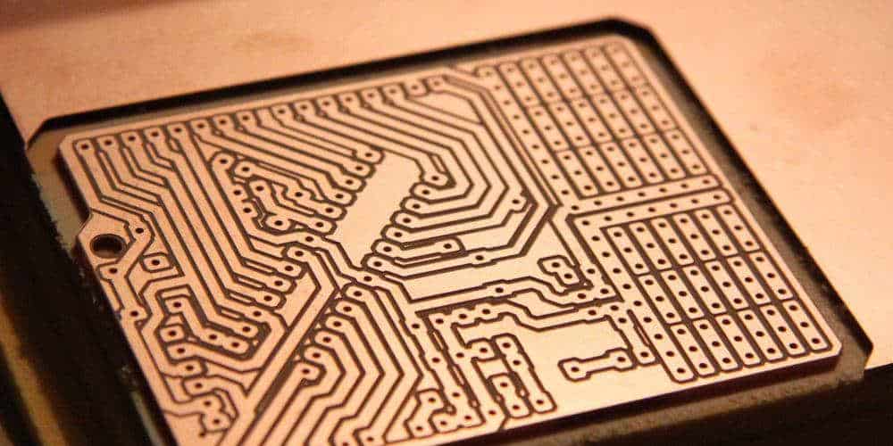
Frist of all, we need to know some basic information about PCB, like copper thickness, circuit width and spacing.
- The Essence of Copper Thickness
Copper, known for its exceptional electrical conductivity, is the lifeblood of any PCB. The copper thickness refers to the amount of copper deposited onto the board’s surface during fabrication. It’s the foundation upon which the traces, the intricate pathways that carry electrical signals, are built. The standard copper thickness is often measured in ounces per square foot (oz/ft²) or micrometers (µm). Common options include 1oz (35µm), 2oz (70µm), and even higher, it depends on customer’s requirement.
- Circuit Width and Spacing
Circuit width and spacing, though often overlooked, are integral components that determine a PCB’s performance, integrity, and overall functionality. Circuit width refers to the dimension of the conductive traces, while spacing pertains to the distance between these traces. These seemingly simple dimensions have a profound impact on the PCB’s behavior.
Secondly, Unveiling the Intricate Relationship
The relationship between copper thickness, circuit width, and spacing is a sophisticated interplay of electrical properties, heat dissipation, and signal integrity. Let’s delve deeper into this complex web of interactions:
Current-Carrying Capacity and Copper Thickness: Copper thickness directly influences a trace’s ability to carry current without succumbing to overheating. Thicker copper translates to higher current-carrying capacity and reduced resistive losses. However, the trade-off is that wider traces are necessary to accommodate the increased copper thickness.
Resistance and Circuit Width: Wider traces exhibit lower resistance, which in turn reduces voltage drop and enhances the efficiency of signal transmission. Designers must strike a balance between trace width, copper thickness, and available board space.
Spacing and Unwanted Interactions: As circuit spacing decreases, the probability of unwanted interactions, such as crosstalk and electromagnetic interference, rises. Thicker copper can exacerbate these issues due to its larger cross-sectional area. Maintaining appropriate spacing between traces is pivotal to prevent signal degradation and maintain integrity.
Heat Dissipation and Trace Width: Thicker copper also aids in better heat dissipation, a crucial consideration for power-intensive applications. However, this can necessitate wider traces to manage the thermal load effectively.
Signal Integrity and Crosstalk: Smaller spacing reduces the risk of crosstalk, but it’s a double-edged sword. Thicker copper traces may introduce higher capacitance, altering impedance and potentially impacting signal integrity. This delicate balance requires careful consideration during design.
For now, we have known the relationship between them, how to develop a best design between the circuit width & spacing and copper thickness, which depends on what’s you really want, the huge current or heat management? Following details should be considered if you want to develop the best circuit width & spacing.
Current Requirements: Start by understanding the current requirements of your traces based on the components and operational conditions. Selecting the appropriate copper thickness and trace width ensures the PCB can handle the anticipated loads.
Thermal Management: Thicker copper facilitates heat dissipation, which is advantageous for power-dissipating components. However, remember that it might necessitate wider traces to ensure effective heat transfer.
Manufacturability: While thicker copper can enhance current-carrying capacity and heat dissipation, it might pose manufacturing challenges. Consult with PCB manufacturers to align your design choices with their capabilities.
Signal Integrity Analysis: Utilize simulation tools to analyze signal integrity, especially when dealing with smaller spacing and thicker copper. These tools provide insights into impedance matching, potential crosstalk, and overall performance.
Flexibility VS Rigidity: While thicker copper enhances many aspects, it can impact the PCB’s flexibility, crucial for certain applications. Evaluate the mechanical demands of your project and strike the right balance.
Regarding metal core PCB in EBest Circuit (Best Technology), the copper thickness and its accordingly circuit width & spacing like below, furthermore, it would be better if you can let me know your copper thickness before checking your drawing, we will give you the best solution before formal production.
| Copper thickness | Minimum circuit width | Minimum circuit spacing |
| 0.5-2oz | 0.25mm | 0.23mm |
| 3oz | 0.35mm | 0.3mm |
| 4oz | 0.4mm | 0.38mm |
Conclusion: Striking the Optimal Balance
The intricate relationship between copper thickness, circuit width, and spacing in PCB design embodies a delicate equilibrium that significantly influences a design’s performance and functionality. This nuanced interplay directly impacts parameters such as current-carrying capacity, resistance, heat dissipation, and signal integrity.
Achieving the optimal balance between these factors requires a deep understanding of electrical properties, thermal considerations, and signal behavior. Designers must carefully evaluate the specific requirements of their projects and leverage simulation tools to fine-tune their choices. Collaboration with PCB manufacturers ensures alignment with manufacturing capabilities.
The dynamic nature of this relationship underscores the constant evolution of PCB technology. As devices become smaller, faster, and more interconnected, the demand for intricate layouts intensifies. Designers must continuously adapt to new challenges, pushing the boundaries of what’s achievable while adhering to the fundamental principles that govern PCB design.


