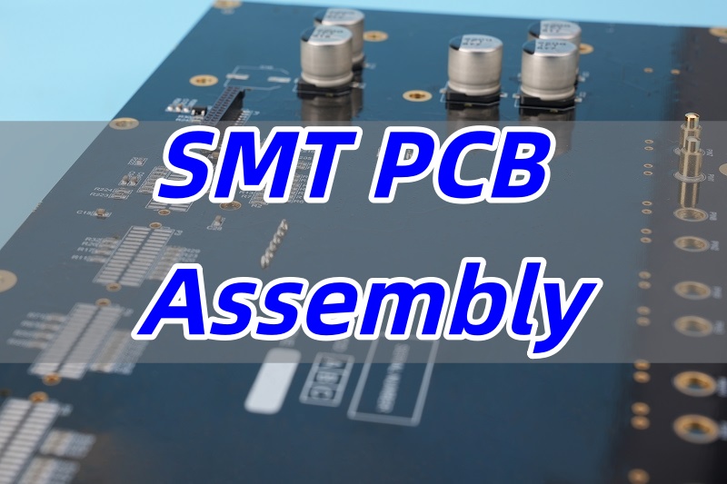
SMT (Surface Mount Technology) is the dominant assembly method in modern electronics manufacturing, enabling compact, high-reliability products. Mastering SMT fundamentals and processes is critical for engineers, manufacturers, and buyers seeking consistent quality in electronic assemblies.
What is SMT?
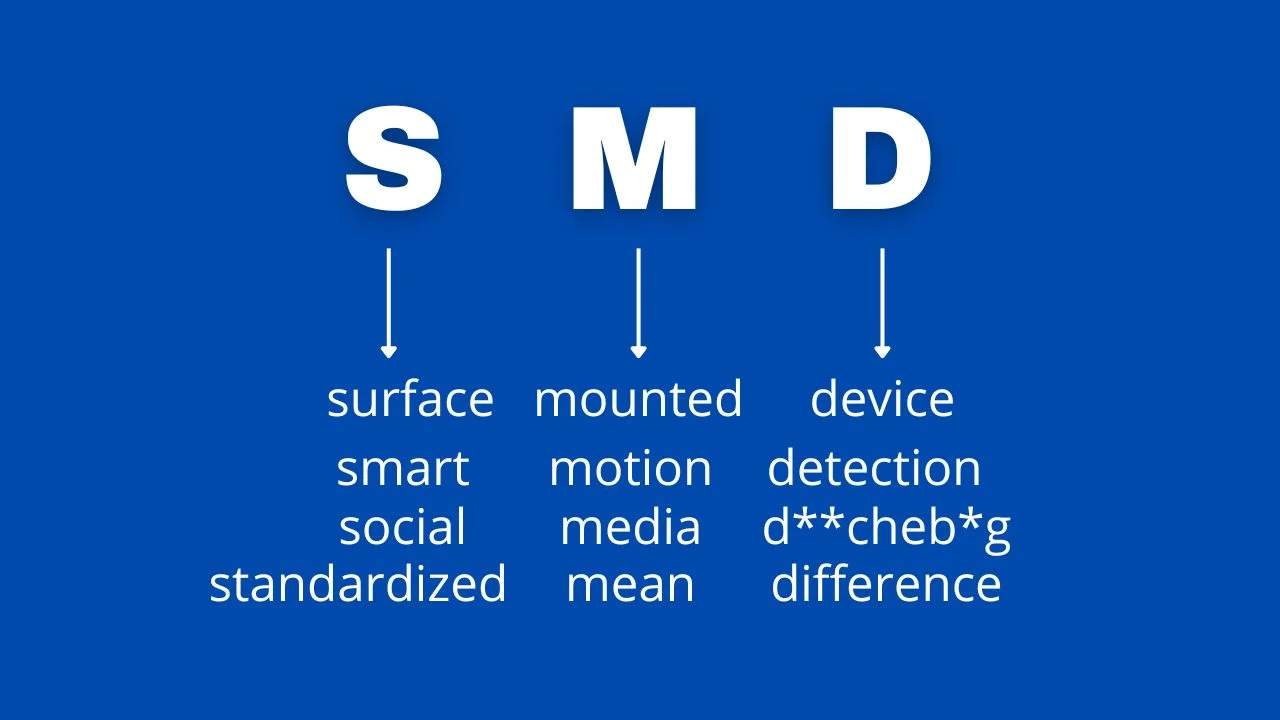
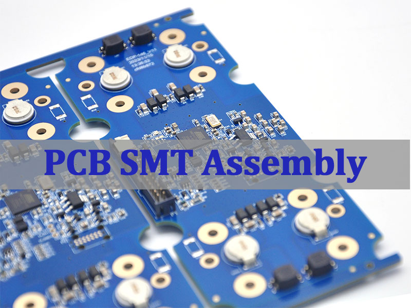
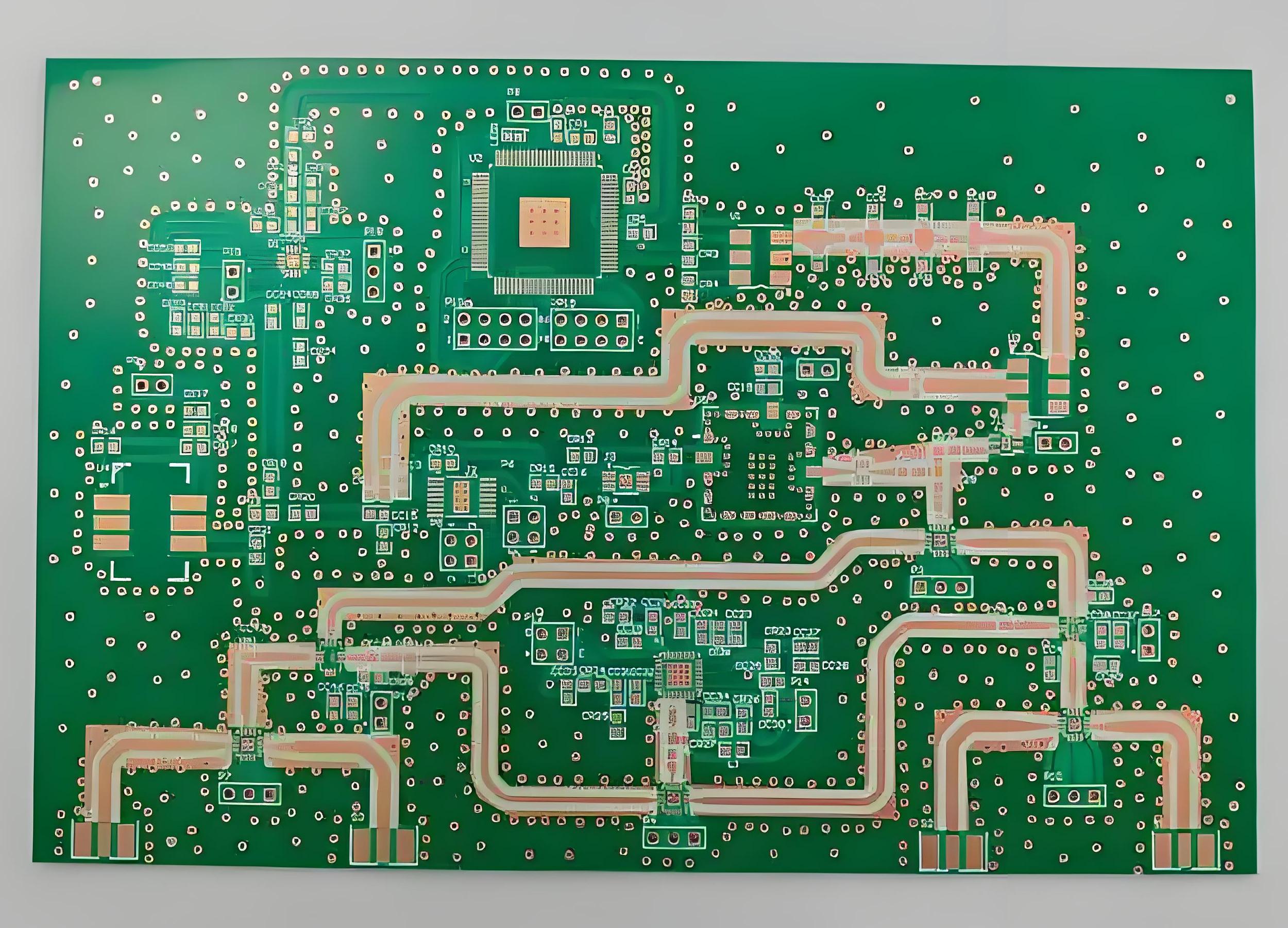
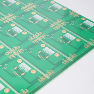
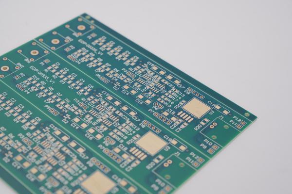
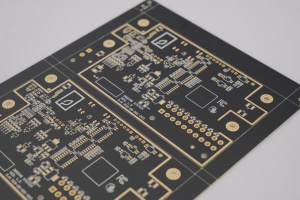
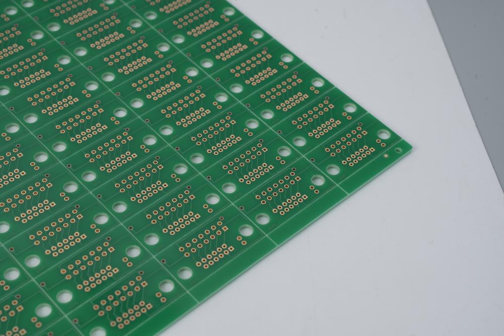
SMT stands for Surface Mount Technology, a core electronic assembly process that mounts surface-mount components (SMDs) directly onto the surface of printed circuit boards (PCBs). It replaces traditional through-hole technology, offering higher assembly density and production efficiency for most electronic devices.
Why is SMT Widely Adopted?
- Enables smaller, lighter electronic products with 40-60% volume reduction compared to through-hole designs.
- Supports high-volume automation, cutting production costs by 30-50% in mass manufacturing.
- Delivers better high-frequency performance and lower electromagnetic interference (EMI).
SMT Meaning
SMT is the abbreviation of Surface Mount Technology, referring to the set of techniques for mounting and soldering SMDs on PCB surfaces without drilling insertion holes. Its core purpose is to achieve reliable electrical and mechanical connections between components and PCBs efficiently.
Key Terminology in SMT
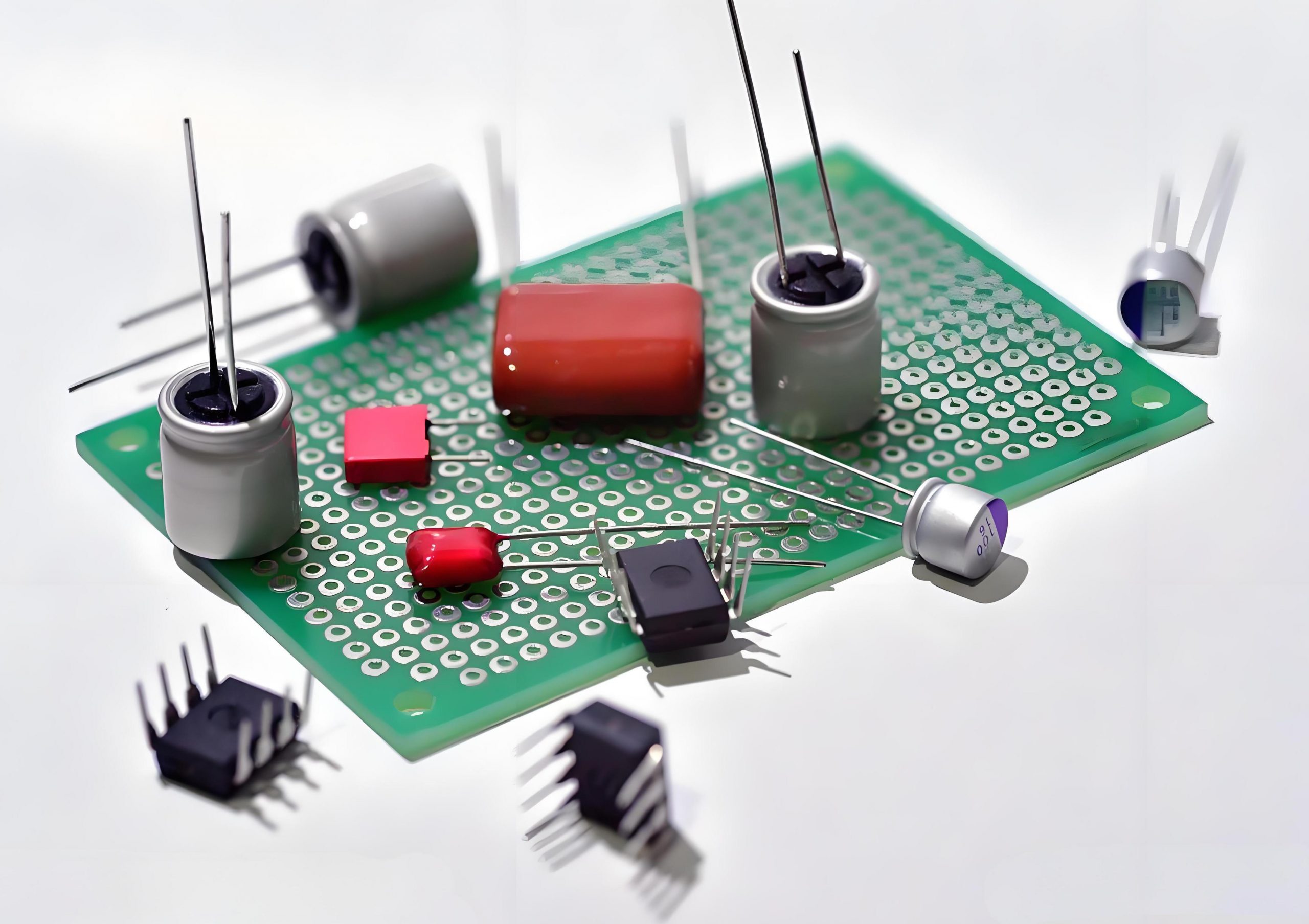
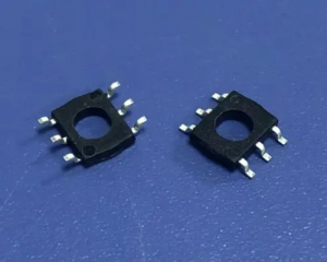
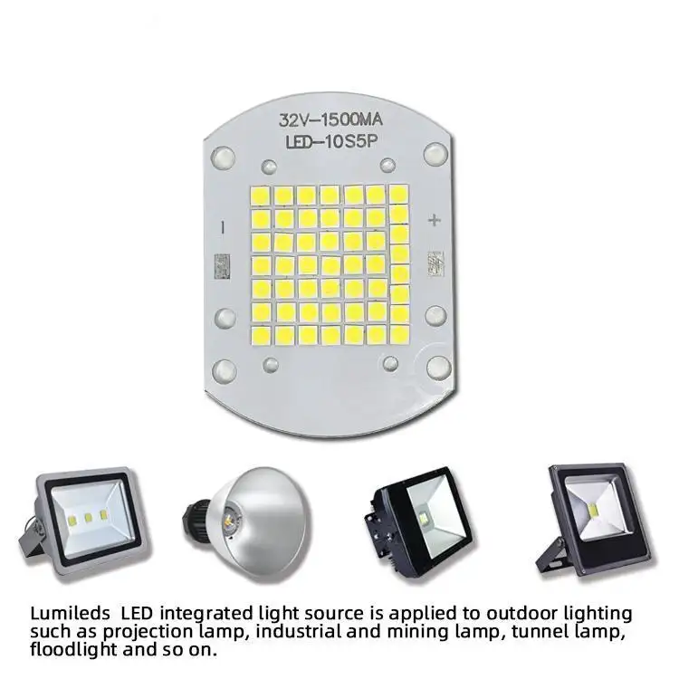
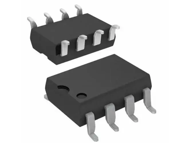
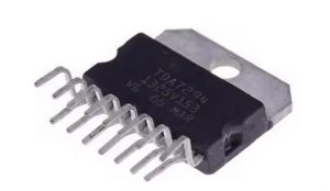
- SMD: Surface Mount Device, the components used in SMT assembly (resistors, capacitors, ICs, etc.).
- PCB: Printed Circuit Board, the base for mounting SMT components.
- Reflow Soldering: The heating process that melts solder paste to bond SMDs to PCB pads.
Definition of SMT
Surface Mount Technology (SMT) is a standardized electronic assembly process that involves applying solder paste to PCB pads, precisely placing SMDs onto the paste, and heating the assembly to form permanent solder joints. It is defined by IPC standards as a high-density, automated assembly method for modern electronics.
Core Characteristics of SMT
SMT eliminates the need for PCB hole drilling for component leads, relying on surface tension and solder paste adhesion to secure components. This results in lower PCB material usage, faster production cycles, and reduced solder joint defect rates compared to traditional methods.
What is SMT in Electronics
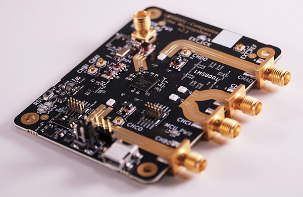
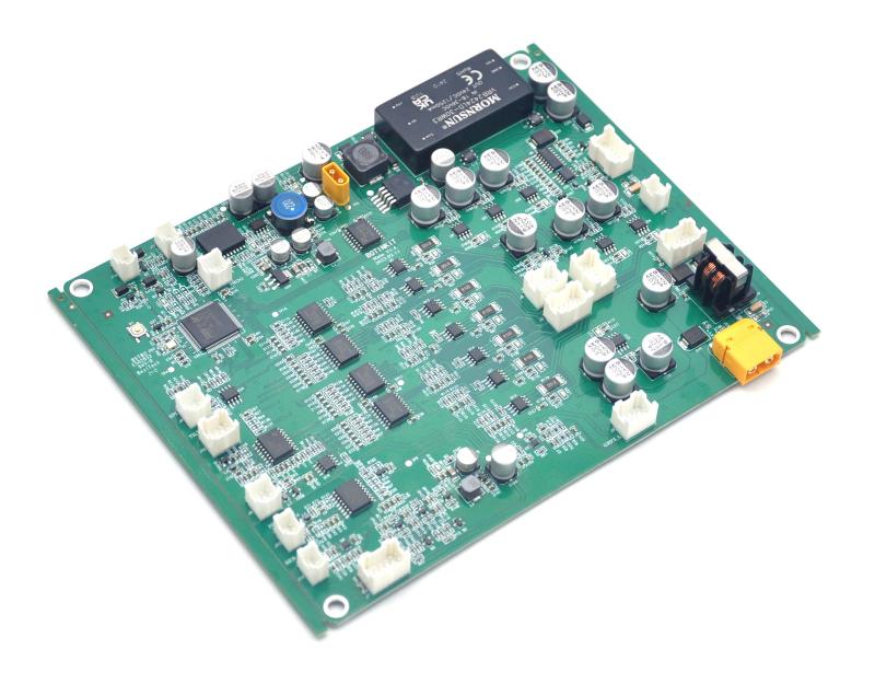
In electronics, SMT is the primary method for assembling PCBs in consumer devices, industrial controls, medical equipment, and communications hardware. It enables the miniaturization of high-performance electronics, from smartphones to 5G base stations.
Common Electronic Applications of SMT
- Consumer electronics: Smartphones, laptops, wearables, and televisions.
- Industrial electronics: PLCs, sensors, and automation controllers.
- Medical devices: Diagnostic tools, wearable monitors, and imaging equipment.
What is SMT in Manufacturing
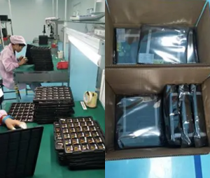
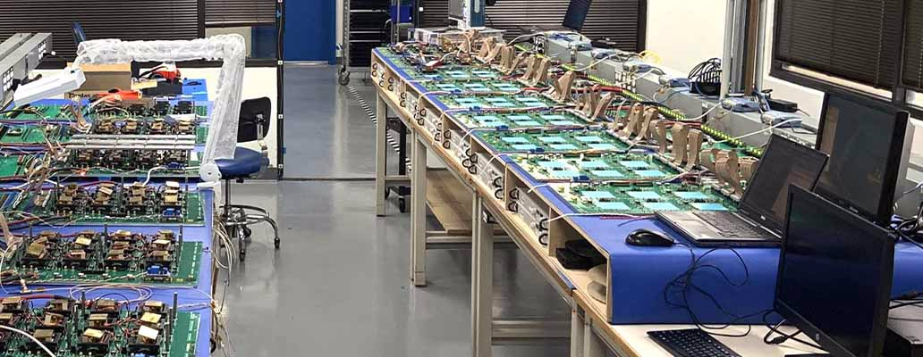
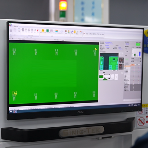
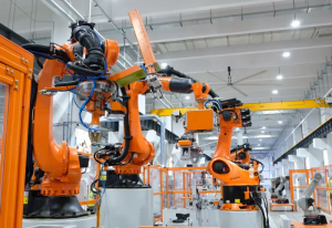
In manufacturing, SMT is a streamlined, automated process that integrates multiple stages—from solder paste printing to inspection—to produce consistent PCB assemblies at scale. It is a cornerstone of lean manufacturing for electronic components.
SMT Manufacturing Workflow Goals
- Achieve high throughput: Up to 30,000 components per hour with advanced placement machines.
- Maintain low defect rates: Targeting <10 ppm (parts per million) for critical applications.
- Ensure process repeatability: Complying with IPC-A-610 and IPC-7351 standards.
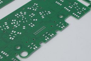
Basic SMT Process Flow
The basic SMT process consists of 6 sequential stages, with each step directly affecting final assembly quality. Front-end process control is critical to reducing defects and ensuring reliability.
What Are the Core Stages of SMT?
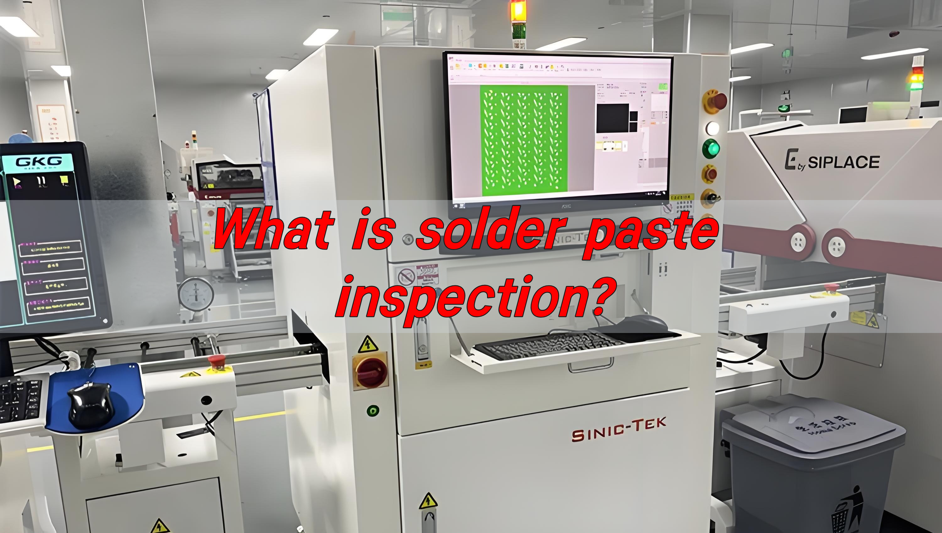
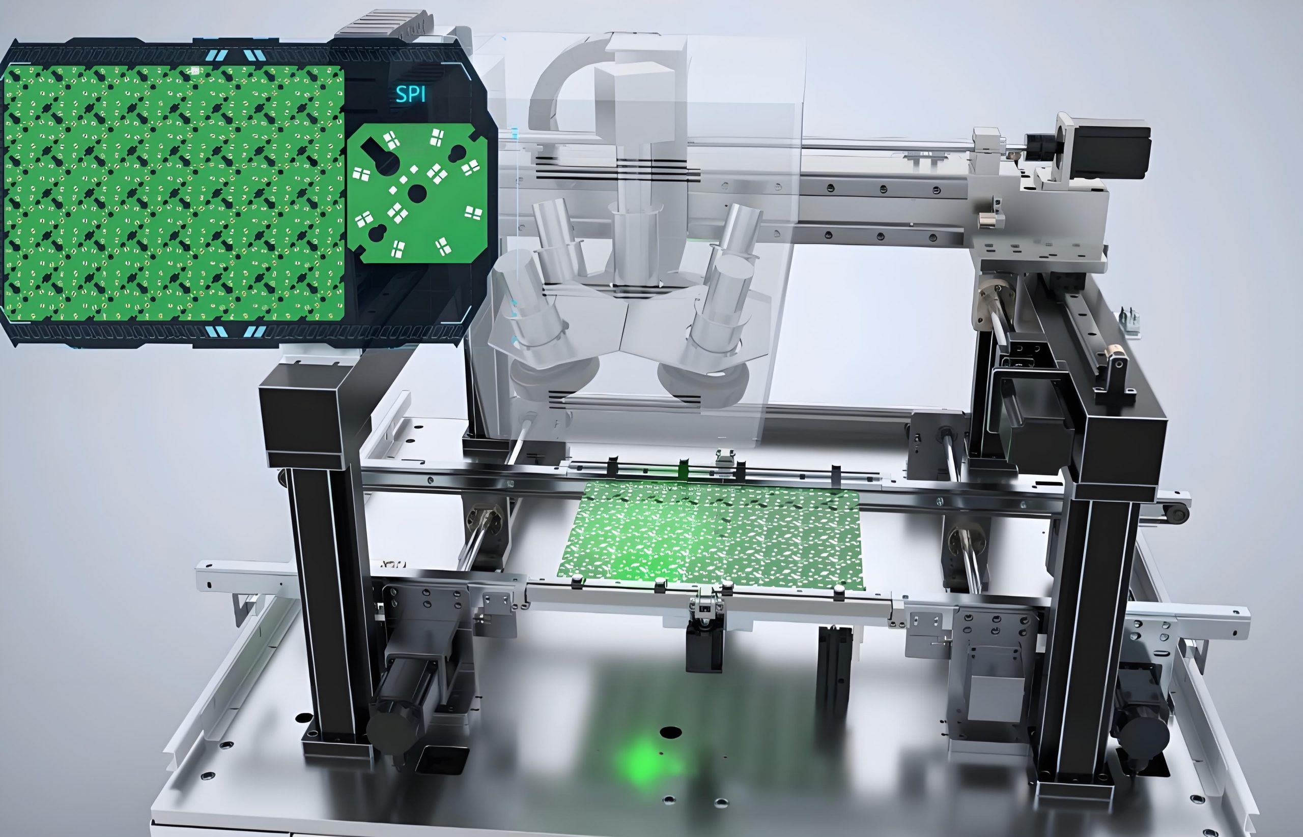
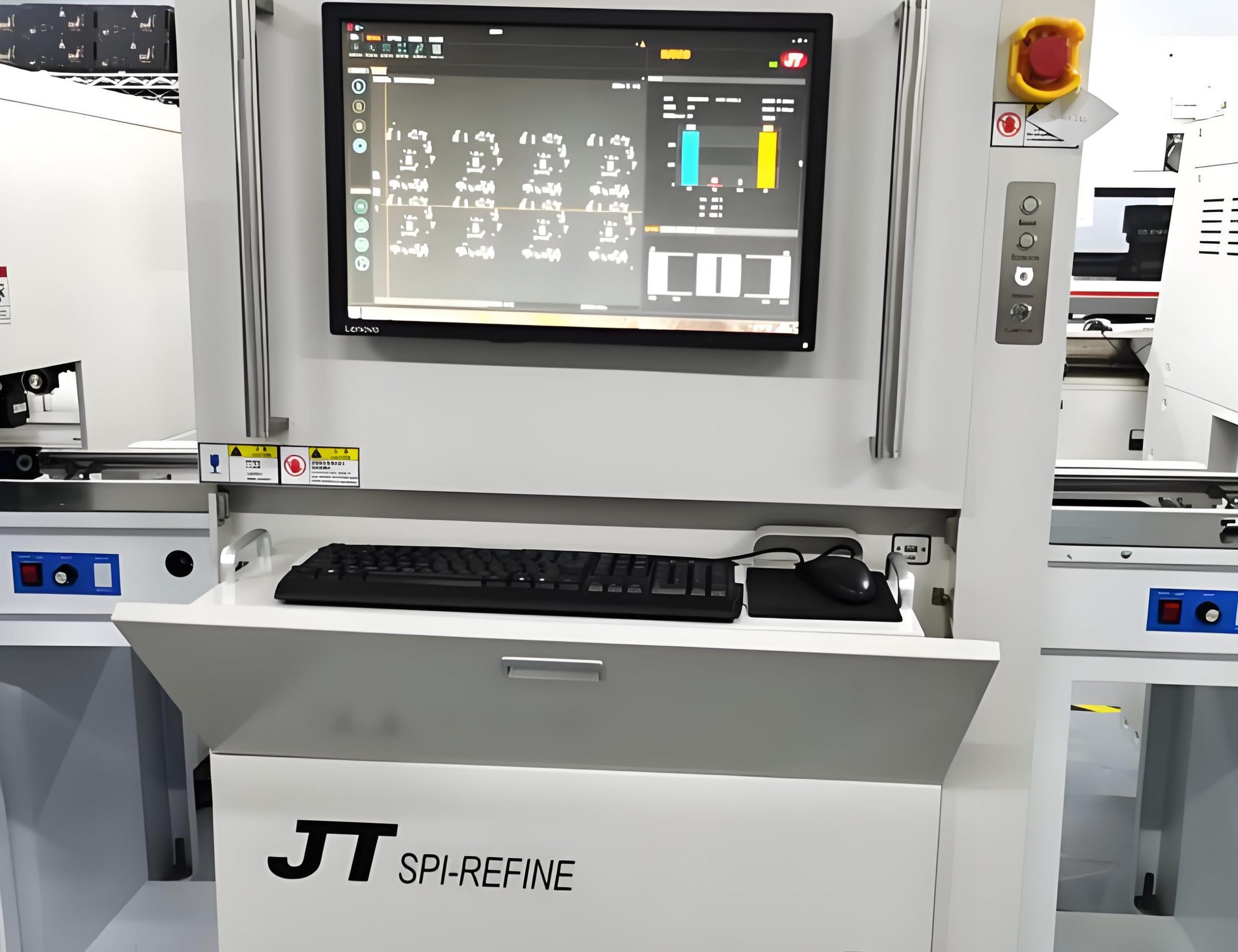
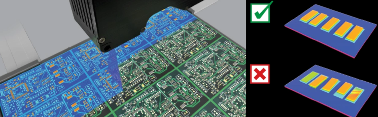
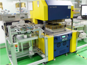
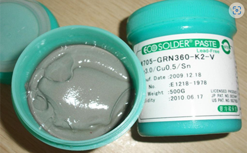
- Solder Paste Printing: Apply solder paste to PCB pads using a stencil, the first gate for welding quality. Laser-cut stencils (±5μm precision) and SPI (Solder Paste Inspection) are mandatory for high-reliability projects.
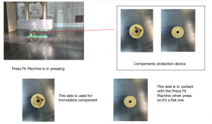
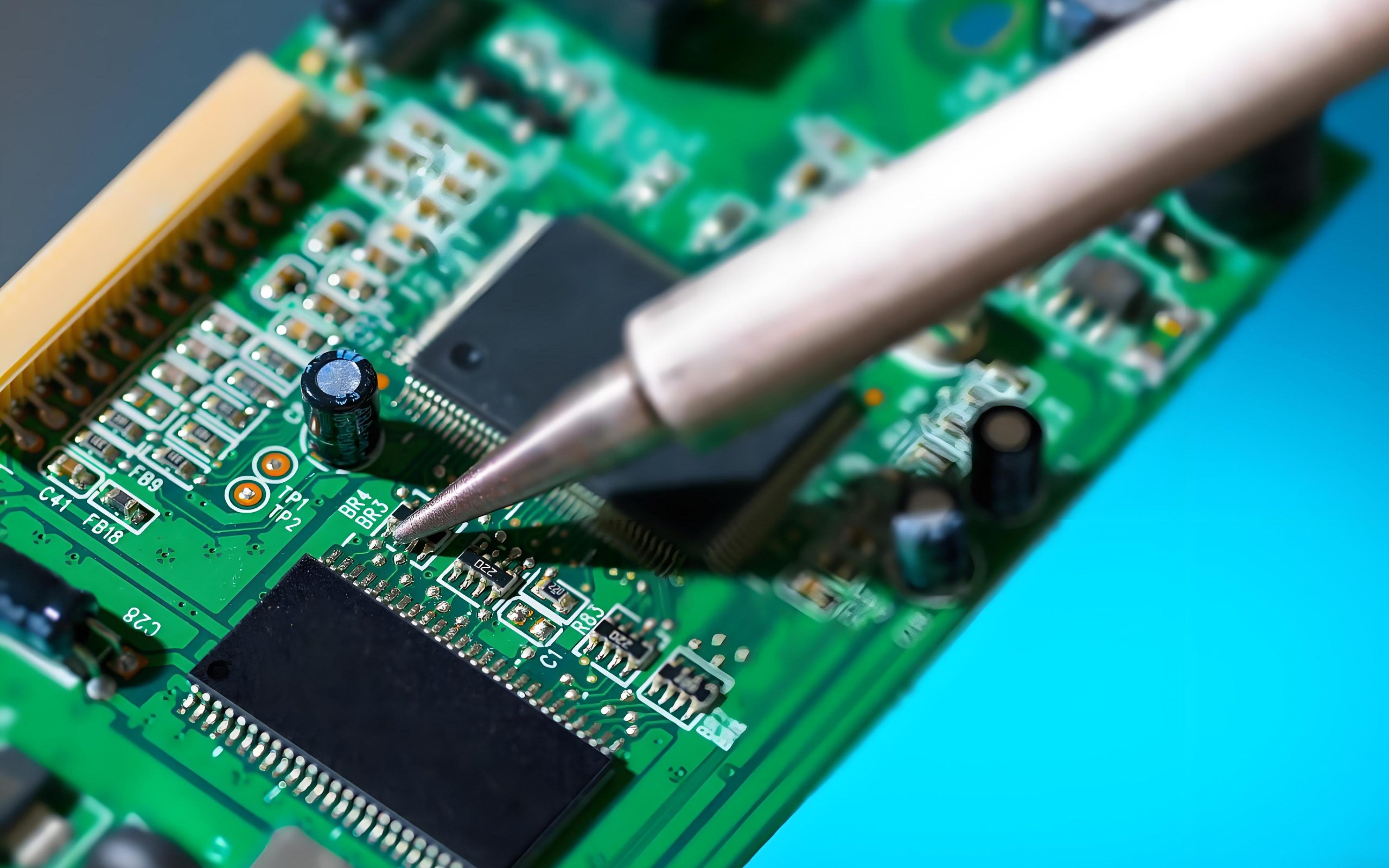
- Component Placement: Use automated machines to place SMDs onto solder paste, requiring repeat accuracy ≤±25μm for 0201-sized components and fine-pitch devices.
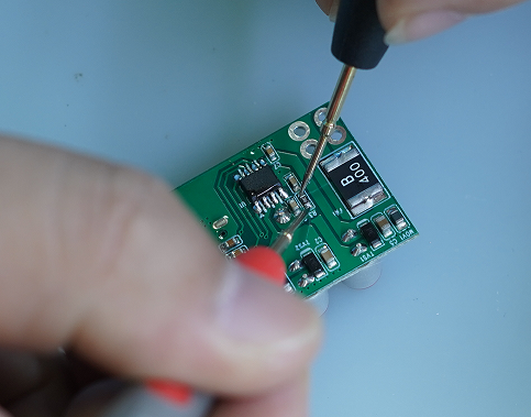
- Reflow Soldering: Heat the assembly to melt solder paste, forming permanent joints. Custom temperature profiles are needed for different PCB thicknesses and component types.
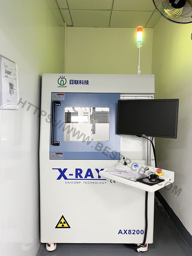
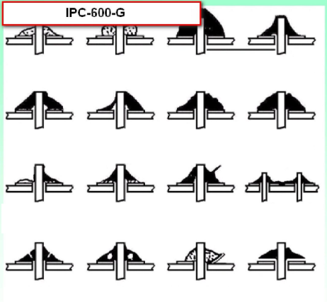
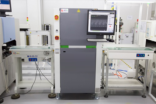
- Inspection & Testing: Combine AOI (surface defects), X-ray (BGA/QFN bottom joints), and FCT (functional verification) to catch hidden issues.
- Cleaning (Optional): Remove flux residues via water or semi-aqueous cleaning, tested per IPC-TM-650 for ion contamination.
- Reliability Enhancement: Implement ESD protection and underfill for advanced packages to improve long-term stability.
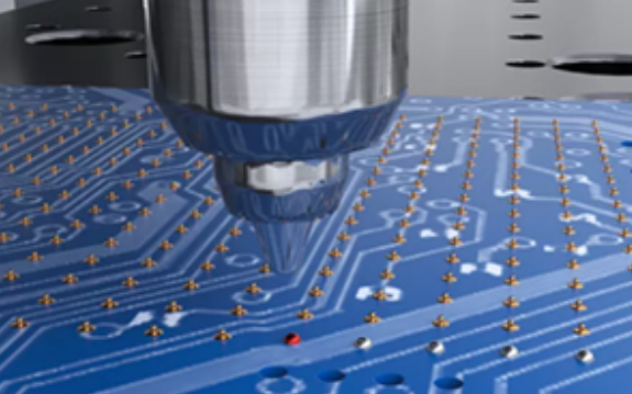
SMT Placement Process
The SMT placement process is a precision-driven step that bridges solder paste printing and reflow soldering, directly impacting component alignment and solder joint integrity.
How to Ensure Accurate SMT Placement?
- Machine Calibration: Regularly calibrate placement machines to maintain ±25μm repeat accuracy, replacing worn nozzles to avoid component slippage.
- Component Recognition: Use advanced vision systems to identify odd-form components and black-body devices, reducing placement errors.
- Double-Side Placement: For double-sided PCBs, prioritize lighter components first to prevent displacement during reflow.
- Real-Time Monitoring: Integrate MES systems to track placement parameters, enabling immediate adjustments for offset or misalignment.
Key Advantages of SMT Over Through-Hole Technology
SMT outperforms traditional through-hole technology in most modern electronics, offering irreplaceable benefits for miniaturization and mass production.
SMT vs. Through-Hole: Core Differences
| Metric | SMT | Through-Hole |
|---|---|---|
| Component Density | 40-60% higher, enabling miniaturization | Low, limited by hole spacing |
| Production Cost | 30-50% lower in high-volume manufacturing | Higher due to manual insertion |
| High-Frequency Performance | Superior, lower EMI | Poor, lead inductance affects signals |
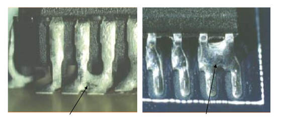
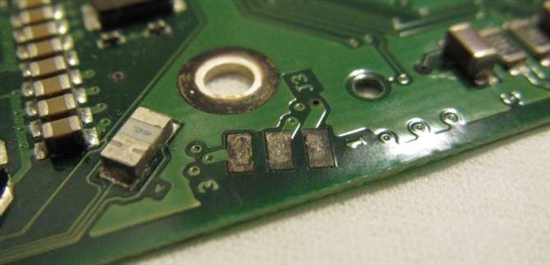
Common SMT Defects and Troubleshooting Tips
Most SMT defects stem from process deviations in printing, placement, or reflow. Targeted troubleshooting reduces rework rates and improves consistency.
How to Fix Top SMT Defects?
- Open Joints/Voids: Adjust stencil aperture and reflow profile; ensure solder paste freshness (≤3 months shelf life).
- Bridging: Reduce stencil aperture size and optimize printing pressure to avoid excess solder paste.
- Tombstoning: Balance solder paste volume on component pads and adjust placement accuracy to ≤1/3 pad offset.
- Cold Solder: Extend reflow soak time to fully activate flux, ensuring peak temperature (240-250℃ for SAC305).
Critical Factors for High-Quality SMT Assembly
Achieving high-quality SMT assembly requires a combination of equipment precision, process control, and material management, aligned with IPC standards.
What Drives SMT Assembly Quality?
- Material Control: Use low-residue solder paste and ESD-safe packaging for sensitive components.
- Process Documentation: Record SPI/AOI reports, X-ray images, and reflow curves for full traceability.
- Operator Training: Certify staff on IPC-A-610 standards to identify and resolve minor process issues.
- Nitrogen Reflow: Adopt nitrogen atmosphere for automotive/medical electronics to reduce oxidation and voids.
SMT FAQ
Below are answers to common SMT questions, addressing pain points in process optimization and quality control.
Frequently Asked Questions About SMT
- What is the acceptable void rate for SMT joints? Industrial-grade applications require <25% void rate for BGA/QFN components, tested via X-ray.
- How often should SMT stencils be cleaned? Clean stencils every 50-100 prints to prevent paste buildup and aperture clogging.
- Can SMT handle double-sided PCBs? Yes—use low-temperature solder paste for the second side to avoid reflowing existing joints.
- What’s the difference between leaded and lead-free SMT? Lead-free (SAC305) requires higher peak temperatures (240-250℃) vs. leaded (210-220℃).
- How to reduce SMT rework rates? Implement SPI at the front end—printing defects account for 70% of total SMT issues.
- Is underfill necessary for SMT? It’s mandatory for fine-pitch BGA and automotive electronics to improve shock and vibration resistance.
- What standards govern SMT assembly? IPC-A-610 (acceptability) and IPC-7351 (component land patterns) are industry benchmarks.
Future Trends of SMT Technology
SMT technology is evolving to meet demands for advanced packaging, high reliability, and smart manufacturing in 2026 and beyond.
What’s Next for SMT?
- Advanced Packaging Integration: Merging SMT with SiP/Chiplet technologies for high-density, high-performance electronics.
- Smart Factory Adoption: Full integration of AI-driven AOI, real-time process monitoring, and MES systems for data-driven optimization.
- Automotive-Grade Focus: Enhancing SMT for AEC-Q100/Q200 compliance, with improved thermal and vibration resistance.
- On-Demand Manufacturing: Flexible SMT lines to support low-MOQ, fast-turnaround projects for AIoT and wearables.
We provide high-quality SMT assembly services, adhering to IPC standards and advanced process controls to ensure reliability for automotive, medical, and industrial electronics. If you need SMT solutions, place your order with us today—reach out via email at sales@bestpcbs.com.