Thin film ceramic PCB is a high-precision ceramic circuit solution used in applications that require fine conductor patterns, stable electrical performance, and reliable high-frequency transmission. This article explains what thin film ceramic PCB is, how it is made, what advantages it offers, and where it is commonly used.
For engineers, one of the biggest challenges in advanced circuit design is balancing miniaturization, accuracy, and signal stability. Standard PCB materials may not always perform well in microwave, RF, or precision analog environments. That is why thin film ceramic PCB has become a preferred option in sectors where dimensional control, low loss, and long-term stability matter.
What Is Thin Film Ceramic PCB?
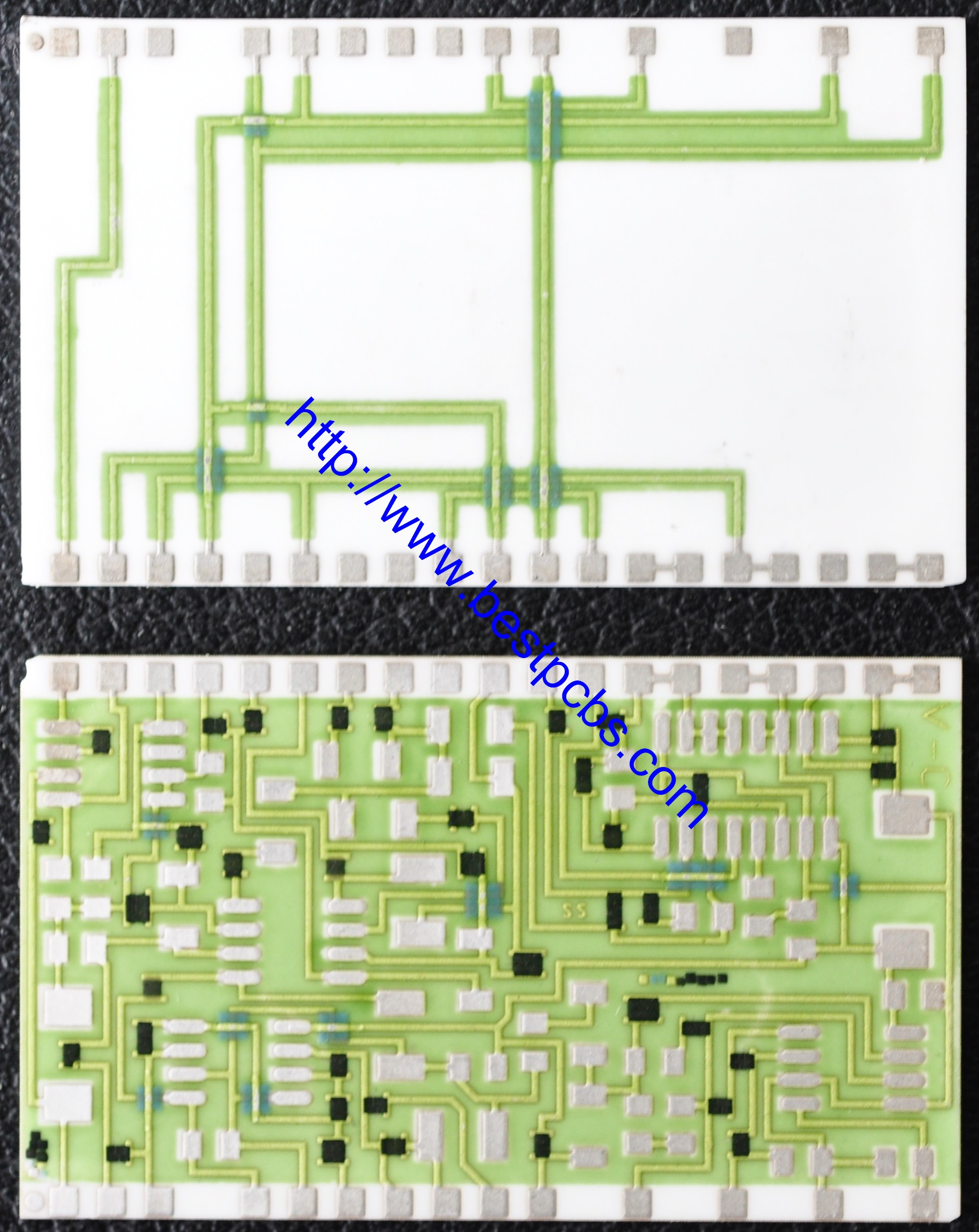
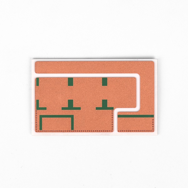
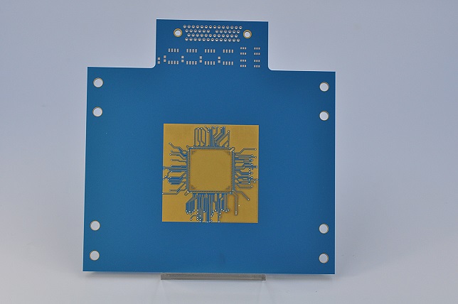
A thin film ceramic PCB is a ceramic-based circuit board made with an ultra-thin conductive layer deposited directly onto the ceramic substrate. In most cases, the conductor thickness is less than 10 μm, which is thinner than that of a thick film ceramic PCB.
This thin conductive layer is formed by advanced deposition technologies such as:
- Physical vapor deposition (PVD)
- Sputtering
- Evaporation
- Electroplating
- Anodic oxidation in selected applications
Because the circuit pattern can be formed with very high precision, thin film ceramic PCB is widely used in compact, high-performance electronic assemblies.
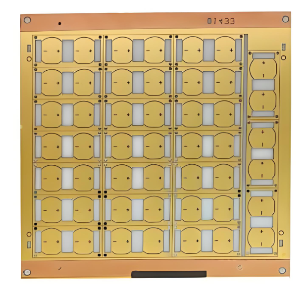
Thin Film Ceramic PCB
How Is Thin Film Ceramic PCB Different from Thick Film Ceramic PCB?
The biggest difference lies in the conductor thickness and fabrication method.
Thin film ceramic PCB uses deposited metal layers with very fine thickness control, while thick film ceramic PCB usually uses printed conductive paste followed by high-temperature firing. Here is a quick comparison between thin film and thick film ceramic PCB:
| Item | Thin Film Ceramic PCB | Thick Film Ceramic PCB |
| Conductor Thickness | Usually below 10 μm | Usually above 10 μm |
| Fabrication Method | Deposition-based | Screen printing and firing |
| Line Precision | Very high | Moderate |
| Circuit Density | Higher | Lower |
| Electrical Accuracy | Excellent | Good |
| Cost | Higher | More economical |
| Best Use | RF, microwave, precision analog | Power circuits, standard hybrid circuits |
In short, thin film ceramic PCB is often selected when the design requires tighter tolerances and better RF behavior.
What Are the Main Characteristics of Thin Film Ceramic PCB?
Compared to thick-film ceramic PCB, the major characteristics of thin-film circuits is the smaller size. However, the manufacturing equipment used is more expensive and the cost of production is higher.
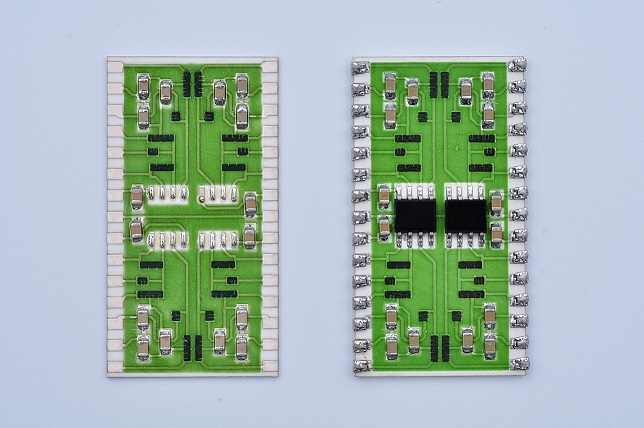
Thin-film Ceramic PCB is suitable for a variety of circuits, especially for analog circuit which need high accuracy, great stability, and excellent performance. Compared with other circuits board, it is more suitable for microwave circuits.
What Types of Thin Film Ceramic Circuits Are There?
Thin film ceramic circuits are often divided into two categories based on passive element behavior.
- Lumped Parameter Circuits
These circuits have passive elements concentrated in specific component regions. They are commonly used from low-frequency applications up to the microwave range.
- Distributed Parameter Circuits
In these designs, electrical parameters are distributed along the circuit geometry itself. This structure is mainly used in the microwave frequency band, where line dimensions directly affect performance.
This classification is especially relevant in RF design, where layout and material selection are closely connected.
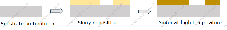
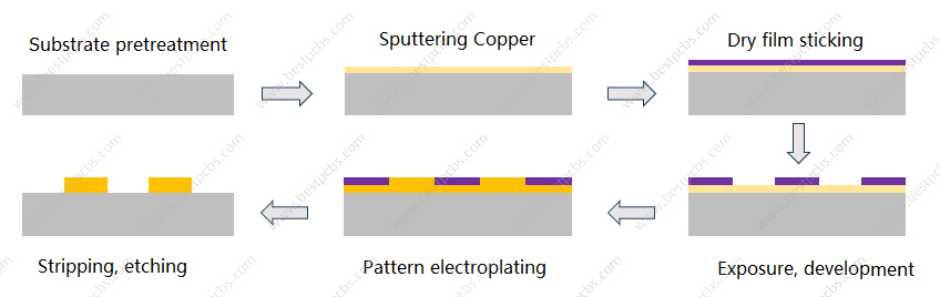
How Is Thin Film Ceramic PCB Manufactured?
Several manufacturing methods can be used to form thin conductive layers on ceramic substrates. The most common process family is physical vapor deposition, while electroplating and anodic oxidation may also be used in selected steps.
PVD is one of the most common methods for making thin film ceramic PCB. It forms metal layers on the ceramic surface inside a vacuum chamber. The two most widely used PVD methods are:
1. Evaporation
In the evaporation process, the source material is heated until it becomes vapor, then it condenses onto the ceramic substrate as a thin and uniform film.
2. Sputtering
In sputtering, particles are ejected from a target material and deposited onto the ceramic surface. This process offers good adhesion, excellent film uniformity, and strong thickness control.
These vacuum-based methods are widely used to create:
- Fine conductive traces
- Resistor films
- Insulating layers
- Protective films
- Passive circuit networks
What Is the Role of Electroplating in Thin Film Ceramic PCB?
Electroplating is often used as a supplementary process. In microwave hybrid integrated circuits, it can increase the thickness of selected thin film conductors, such as microstrip lines.
This helps improve:
- Current-carrying capability
- Conductor performance
- Power efficiency
- Signal transmission in certain RF structures
Electroplating is not always the main film-forming step, but it plays an important role in performance tuning.
What Is the Role of Anodic Oxidation?
Anodic oxidation is less commonly used than PVD, but it still has value in special thin film applications.
It can be used to:
- Form dielectric films
- Improve insulation in specific areas
- Adjust the resistance value of some thin film resistors
For highly customized circuit structures, anodic oxidation can support better control of electrical properties.
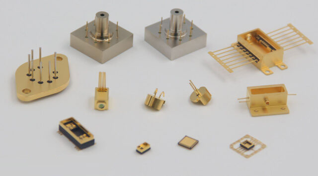
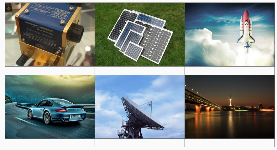
Where Is Thin Film Ceramic PCB Used?
Thin film ceramic PCB is used in products where accuracy, stability, and high-frequency behavior are critical.
Typical applications include:
- RF modules
- Microwave circuits
- Hybrid integrated circuits
- Precision analog circuits
- Sensors
- Aerospace electronics
- Medical electronics
- Telecom equipment
- Defense and instrumentation systems
These applications often require materials and circuit structures that can maintain performance under temperature change, frequency stress, and long operating cycles.
Why Is Thin Film Ceramic PCB Suitable for RF and Microwave Applications?
Thin film ceramic PCB is especially suitable for RF and microwave designs because it combines:
- Fine conductor geometry
- Stable substrate performance
- Low dimensional variation
- Good high-frequency consistency
- Strong thermal stability
In microwave circuits, even small variations in line width or conductor thickness can affect impedance and signal loss. Thin film technology helps reduce that variation and supports more predictable performance.
FAQ
1. What is the conductor thickness of thin film ceramic PCB?
In most cases, the conductor thickness of a thin film ceramic PCB is less than 10 μm. That is one of the main distinctions between thin film and thick film ceramic technologies.
2. Is thin film ceramic PCB better than thick film ceramic PCB?
It depends on the application. Thin film ceramic PCB is better for high precision, RF, microwave, and compact circuit designs. Thick film ceramic PCB is often more suitable for cost-sensitive or less demanding designs.
3. Can thin film ceramic PCB be used in analog circuits?
Yes. Thin film ceramic PCB is widely used in precision analog circuits because of its stable electrical performance and fine pattern accuracy.
4. Why is thin film ceramic PCB more expensive?
The cost is higher because the process requires vacuum equipment, advanced deposition technology, and tighter manufacturing control.
5. Is thin film ceramic PCB suitable for microwave circuits?
Yes. It is one of the preferred solutions for microwave circuits because it supports fine features, stable conductor behavior, and strong high-frequency performance.
Why Choose EBest Circuit for Thin Film Ceramic PCB?
EBest Circuit has extensive experience in advanced ceramic PCB manufacturing and custom circuit solutions for demanding electronic applications. We understand that thin film ceramic PCB projects often require more than basic fabrication. They need careful material selection, precise process control, and strong engineering support from design to production.
What we can offer includes:
- Professional ceramic PCB manufacturing experience
We support a wide range of ceramic circuit requirements, including high-precision and high-reliability applications.
- Engineering-driven support
Our team works closely with customers on material choice, stack-up suggestions, manufacturability review, and process optimization.
- Support for complex applications
We understand the needs of RF, microwave, hybrid, medical, and industrial customers who require stable and repeatable circuit performance.
- One-stop service
From PCB fabrication to assembly support, we help simplify the supply chain and reduce project coordination pressure.
- Quality-focused manufacturing
We emphasize process consistency, inspection control, and reliable delivery to support both prototype and production needs.
If you are looking for a dependable thin film ceramic PCB manufacturer, EBest Circuit is ready to support your project with practical engineering advice and responsive service.
Contact us at sales@bestpcbs.com for technical discussion and quotation support.