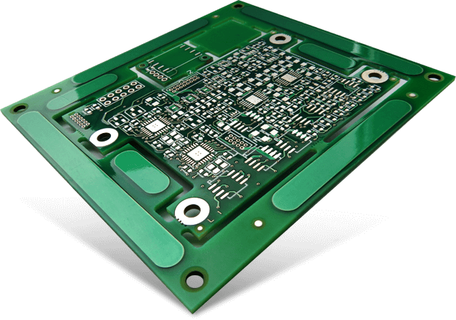
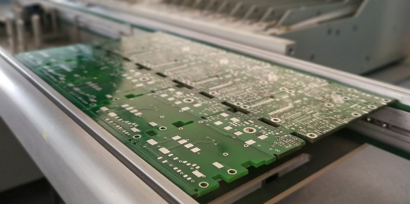
Copper clad laminate (CCL) is crucial in printed circuit boards (PCBs), providing structural integrity and conductivity. Whether you are a PCB designer, engineer, or manufacturer, understanding CCLs will help you choose the right materials for your applications. In this guide, we explore CCL types, uses, and pricing, along with an in-depth look at its manufacturing process.
EBest Circuit (Best Technology) offers comprehensive PCB manufacturing solutions, seamlessly integrating design, prototyping, assembly, component sourcing, and 360° technical support across the entire project lifecycle. Leveraging advanced lamination systems and high-precision CNC drilling machines from Hitachi and Timax, we ensure exceptional accuracy in multilayer PCB fabrication. Backed by a seasoned R&D team and engineers with over 10 years of industry experience, we guarantee a prompt response within 12 hours. Punctual delivery is our commitment, ensuring your projects stay on track. Feel free to reach out to us at sales@bestpcbs.com for any copper-clad laminate PCB needs.
What is Copper Clad Laminate?
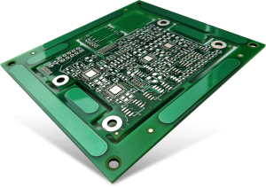
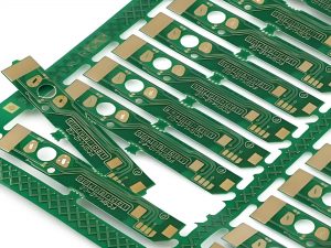
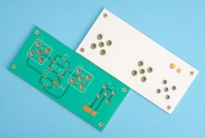
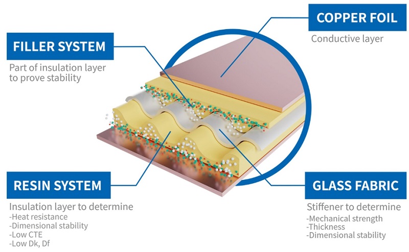
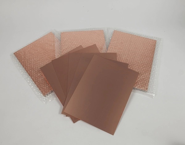
Copper clad laminate (CCL) is a composite material made of a non-conductive substrate (such as fiberglass, resin-impregnated paper), filler, and other chemicals, with a thin copper foil layer bonded to one or both sides. It serves as the foundation for PCB fabrication, ensuring electrical pathways are properly formed while offering mechanical support. CCLs are widely used in consumer electronics, automotive applications, and industrial equipment.
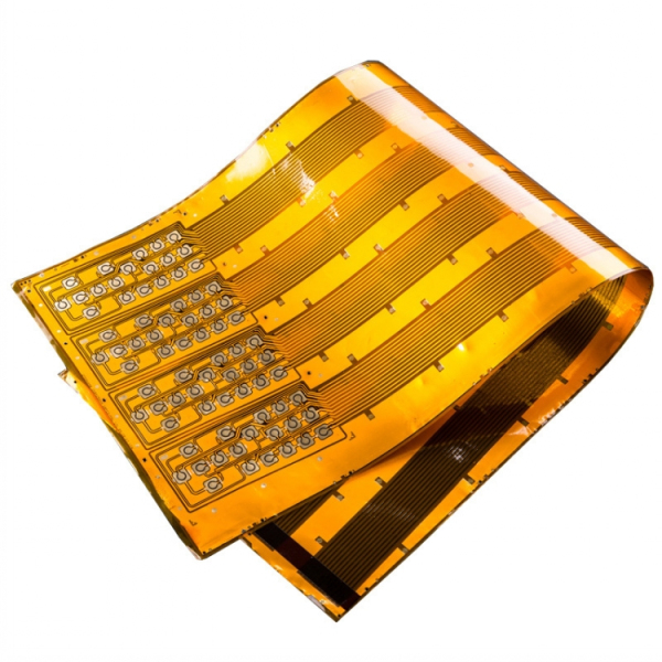
What is Flexible Copper Clad Laminate?
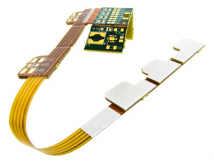
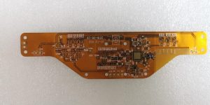
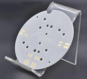
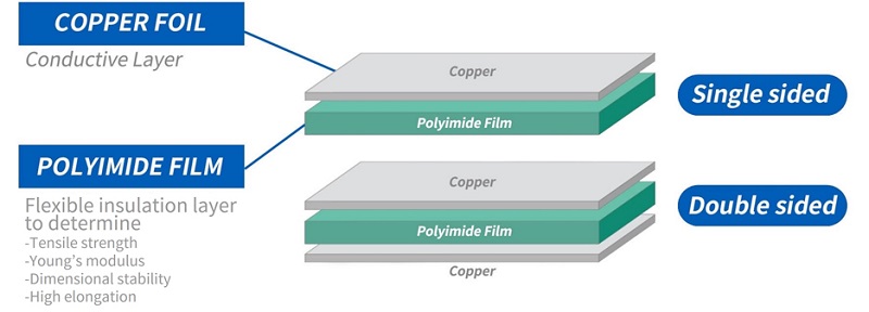
Flexible copper clad laminate (FCCL) is a variation of CCL that uses a flexible substrate instead of rigid fiberglass. The most common substrate materials include polyimide or polyester, and FCCL is produced by laminating copper foil onto polyimide film (PI), making FCCLs suitable for bendable and lightweight applications. These laminates are commonly found in wearables, foldable devices, and medical electronics, where flexibility is a key requirement.
What is Copper Clad in PCB?
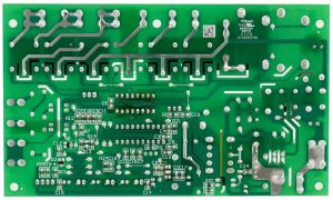
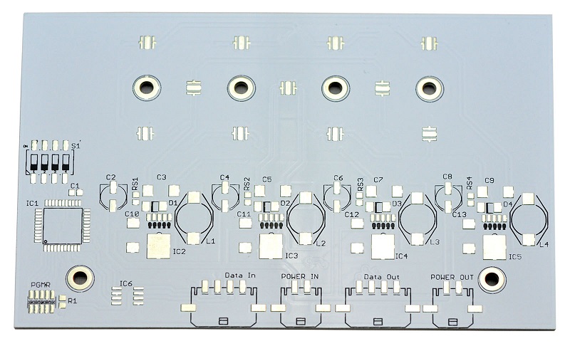
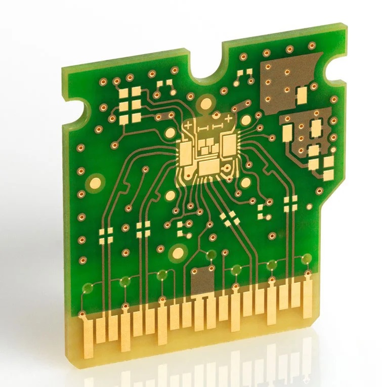
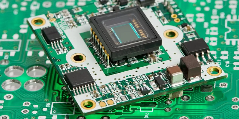
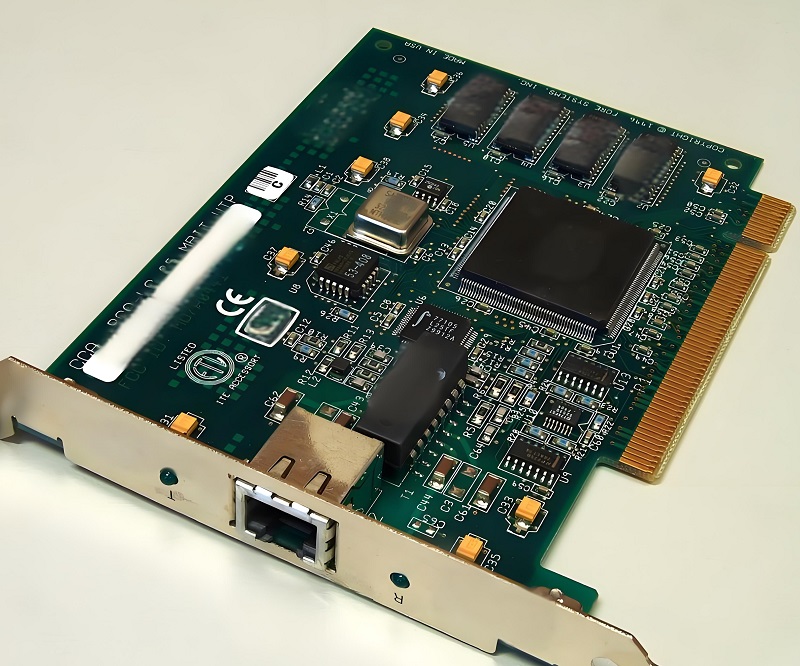
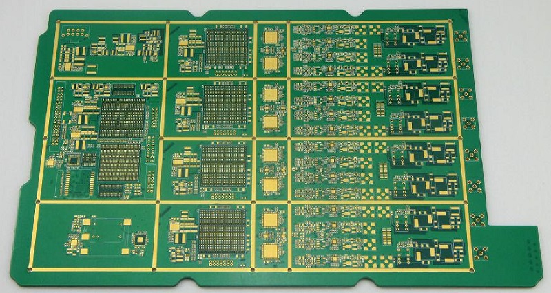
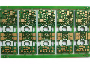
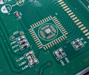
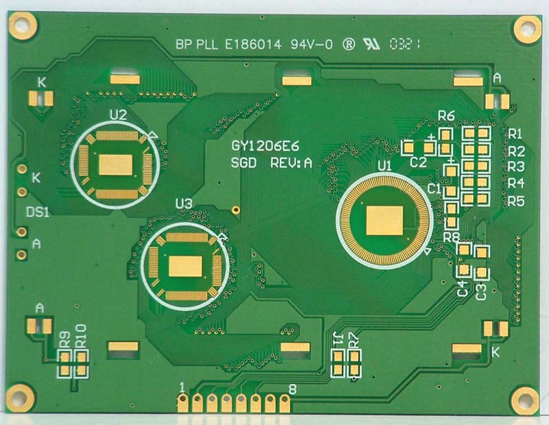
In PCB manufacturing, copper clad laminate acts as the base material that undergoes etching, drilling, and layering processes to create functional circuits. The copper layer allows for efficient electrical conductivity, while the substrate provides insulation and mechanical support. PCBs can have single-sided, double-sided, or multi-layer configurations, depending on design complexity.
What are the Different Types of Copper Clad Laminate?
There are several types of CCLs, each designed for specific performance requirements:
- FR-4 – The most widely used CCL, composed of woven glass fabric and epoxy resin, offering excellent electrical insulation and thermal resistance.
- CEM-1 – A cost-effective option with a paper-based core and fiberglass reinforcement, ideal for single-sided PCBs.
- CEM-3 – Similar to FR-4 but with a finer glass weave, providing better flexibility and processing ease.
- Flexible Copper Clad Laminate (FCCL) – Uses polyimide or polyester as a base, enabling use in applications requiring bending or flexing.
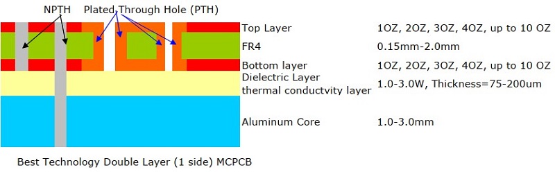
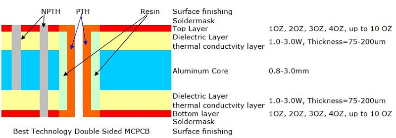
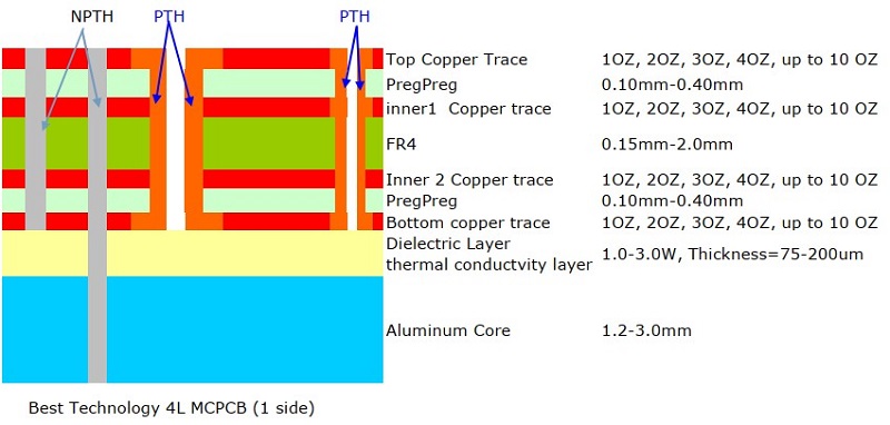
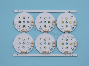
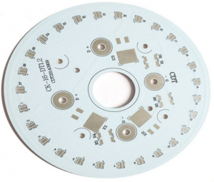
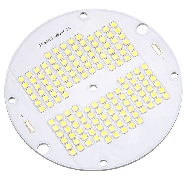
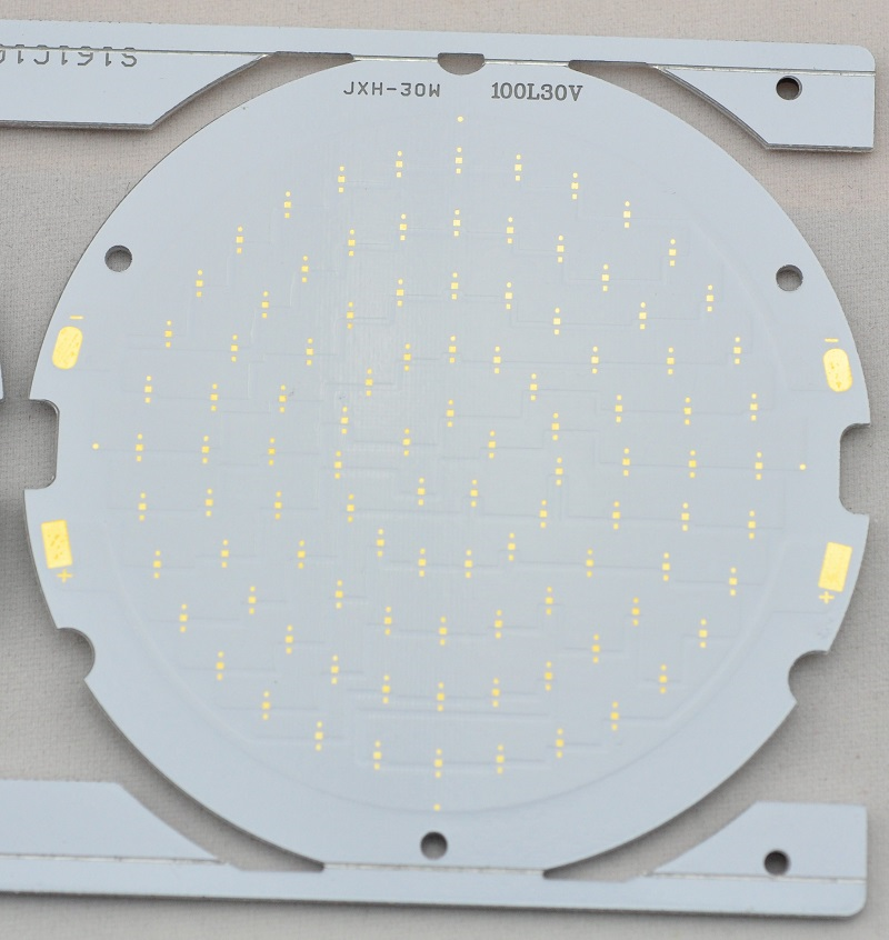
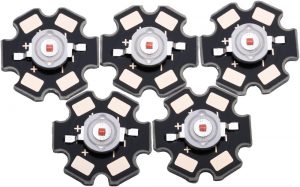
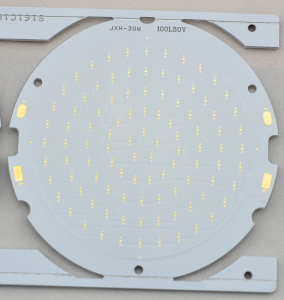
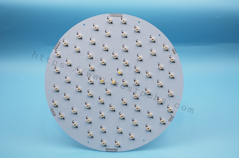
- Metal Core CCL – Features an aluminum or copper core for better heat dissipation, commonly used in LED lighting and power electronics.
- High-Frequency CCL – Designed for RF and microwave applications, using PTFE or ceramic-based substrates for improved signal integrity.
What is the Difference Between Copper and Copper Clad?
Copper is a pure metal known for its excellent electrical and thermal conductivity. Copper clad laminate, however, is a composite material where a thin copper layer is bonded to an insulating substrate. While pure copper is used in electrical wiring and heat exchangers, copper clad laminates serve as the base for PCBs, allowing for structured circuit pathways while maintaining mechanical stability.
What is the HS Code for Copper Clad Laminates?
The Harmonized System (HS) code 7410.11 is widely used for copper clad laminates in international trade. This classification applies to materials consisting of copper foil (printed or unprinted) bonded to an insulating substrate such as fiberglass, epoxy resin, paper, or other dielectric layers.
- 7410.11: Covers copper foil laminated with insulating materials, regardless of surface patterning. These laminates serve as core materials for manufacturing printed circuit boards (PCBs), enabling electrical conductivity and structural support.
Critical Considerations:
- Regional Variations: Some jurisdictions classify PCB-ready laminates (pre-etched or pre-engineered for circuitry) under 8547.20 (“printed circuits”).
- Example: China may categorize advanced laminates under 8547.20 if they are explicitly designed for PCB production.
- Material-Specific Codes: Laminates with plastic-based substrates (e.g., phenolic resin) might fall under 3921.90 (“plastic laminates”).
Verification: Pls consult local customs or a licensed broker for binding rulings in necessary situation, as interpretations vary. For instance:
- U.S. HTS: May use 7410.11.0000 for basic laminates.
- EU TARIC: Could require additional subcodes based on thickness or resin type.
What is the Price of Copper Clad?
Copper clad laminate price varies based on copper thickness, substrate type, material grade, order volume, and market demand. For PCB buyers, this material cost is only one part of the final PCB quotation, but it can strongly affect FR4 PCB, high-frequency PCB, heavy copper PCB, and other custom board projects. Here are the key factors that impact pricing:
- Copper Thickness – Thicker copper layers increase cost due to the higher material requirement.
- Substrate Material – FR-4 is pricier than paper-based laminates like CEM-1.
- Processing Complexity – Advanced CCLs with high-frequency capabilities cost more to manufacture.
- Market Demand – Prices fluctuate based on raw material availability and global market trends.
- Order Volume – Bulk purchases typically come with lower unit costs.
Standard FR-4 CCLs typically range from $5 to $15 per square meter, while high-performance laminates designed for RF applications can cost significantly more.
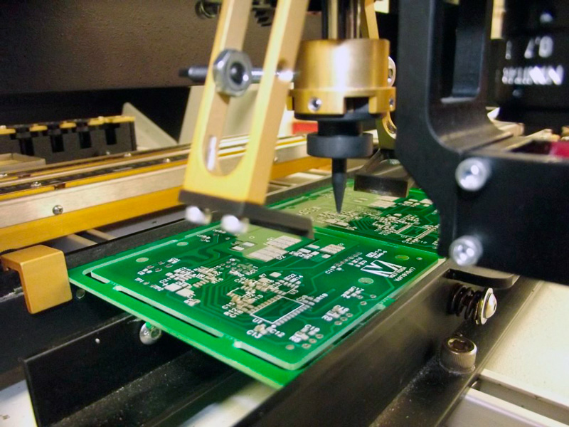
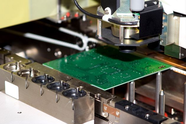
What is the Manufacturing Process of Copper Clad Laminate?
What is copper clad laminate manufacturing process? Manufacturing copper clad laminate involves precise processes to ensure consistent quality and performance. Here take the double-sided copper clad laminate as a case. The production of double-sided copper clad laminates generally follows these steps:
1. Film Printing – Prepare and print the design film.
2. Board Cutting – Cut the board to size, keeping a 20mm process edge.
3. Drilling – Set the board thickness to 2.0mm or 1.6mm, ensuring the drill tip is 1-1.5mm above the PCB surface. Use Create-DCM software to generate U00 format drill files for CNC machines.
4. Polishing – Remove surface oxidation, oil stains, and burrs from drilling.
5. Hole Inspection – Ensure hole clarity for proper chemical penetration. Inspect the drilled and polished board under light to check if the holes are clear and unobstructed.
6. Pre-soaking – Remove oil, oxidation, and copper powder while adjusting the charge for better carbon particle adsorption.
7. Water Rinsing – Thoroughly rinse with clean water to remove chemical residues.
8. Drying – Eliminate residual moisture inside the holes using a drying oven or electric blower.
9. Activation – Coat the inner hole walls with nano-carbon particles to enhance conductivity.
10. Through-Hole Processing – Remove excess activation liquid to ensure all holes remain open using a vacuum cleaner.
11. Curing – Secure carbon particles to the hole walls and dry them with airflow.
12. Repeat Steps 9-11 for better adhesion.
13. Micro-etching – Remove excess carbon particles and wipe off black residues from the copper surface.
14. Water Rinsing – Clean the board thoroughly.
15. Copper Plating – Immerse in a copper plating bath for 20-30 minutes at a current of approximately 3-4A/d㎡ (adjust as needed). This process ensures electrical conductivity by plating copper on the hole walls.
16. Water Rinsing – Clean the surface after plating.
17. Drying – Dry the board and remove any residual moisture in the holes.
18. Lamination – Apply the dry film using a lamination machine.
19. Exposure – Expose the film to light for approximately 3 minutes. Align the film (negative film at this stage) with the board first. Ensure correct alignment of the negative film for double-sided circuits.
20. Developing – Remove unexposed film in a developing solution at 45-50°C while observing changes on the board.
21. Water Rinsing – Rinse thoroughly to remove residues.
22. Etching – Etch at 45-50°C to remove unwanted copper.
23. Water Rinsing – Wash off any remaining etchant to prevent further corrosion.
24. Stripping – Use a strong alkaline solution to remove the dry film.
25. Water Rinsing – Rinse thoroughly.
26. Drying – Dry the board completely.
27. Tin Plating – Perform micro-etching, rinsing, and tin plating to protect exposed copper areas from oxidation and improve solderability.
28. Edge Cutting – Trim off excess material from the fabricated board based on the circuit outline and smooth the board edges using a manual grinding tool.
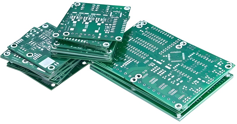
This process ensures high-quality double-sided copper clad laminate for various PCB applications.
Copper Clad Laminate Manufacturers
Several manufacturers produce high-quality copper clad laminates for different industries. Some of the leading names include:
- Doosan Corporation Electro-Materials – A global leader in FR-4 and high-performance CCL production.
- Shengyi Technology – Specializes in advanced CCLs for high-frequency and RF applications.
- Rogers Corporation – Renowned for high-frequency laminates used in 5G and aerospace applications.
- DuPont – Known for high-reliability materials like polyimide-based CCLs for flexible circuits and high-temperature applications.
EBest Circuit (Best Technology) Primarily dedicated to PCB manufacturing, we also source and supply copper clad laminates, providing customers with reliable materials tailored to their specific requirements.
In conclusion, copper clad laminate plays a vital role in PCB manufacturing, influencing performance, cost, and durability. Understanding its manufacturing process, types, and pricing helps engineers and buyers make better decisions. Whether you need rigid FR-4 laminates or flexible options for advanced applications, choosing the right material ensures optimal performance and reliability.
For those sourcing copper clad laminates, partnering with a reputable manufacturer guarantees high-quality materials and consistent supply. We provide one-stop PCB manufacture service, including PCB assembly and component purchasing and all-around technical support before and after-sales. Just feel free to reach out to us at sales@bestpcbs.com for any printed circuit board needs.