PCB manufacturing PCB manufacturing
Home > Blog

rogers pcb

UHDI PCB Fabrication for 80 GHz RF Applications
Friday, June 5th, 2026

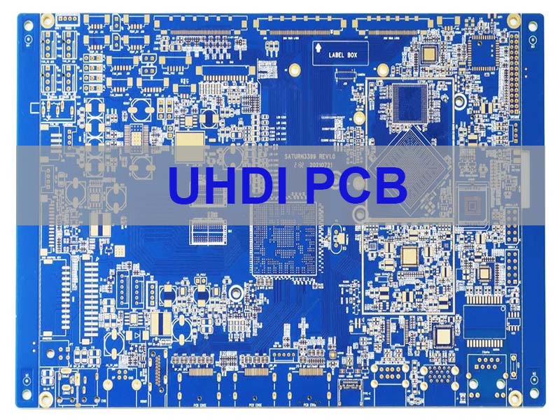
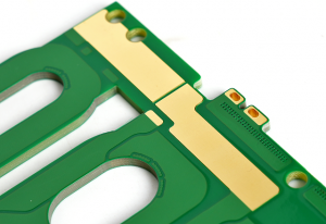
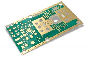
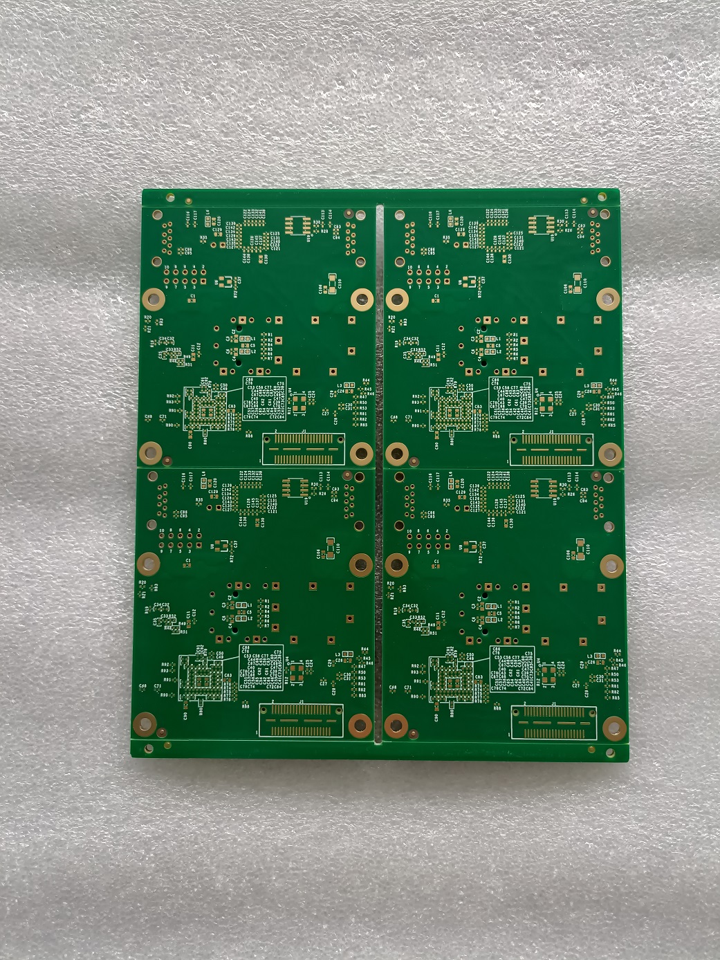
UHDI PCB fabrication is used when a printed circuit board needs extremely high routing density, fine interconnects, short signal paths, and stable performance in compact high-frequency or high-speed systems. For projects operating around 80 GHz, the board is no longer just a dense interconnect platform. It also becomes part of the RF signal path, where material loss, stack-up stability, copper profile, impedance control, microvia quality, and fabrication tolerance can directly affect performance.

EBest Circuit (Best Technology) is an engineer-oriented one-stop PCB service provider supporting UHDI PCB fabrication, high-frequency material review, DFM review, PCB layout manufacturability feedback, preliminary stack-up review, controlled impedance, PCBA assembly, testing, and production documentation based on customer-provided files. If you are preparing a UHDI PCB prototype or volume project using Megtron 6, Rogers, or other low-loss materials, you can send your available files to sales@bestpcbs.com for engineering review and quotation support.

UHDI PCB

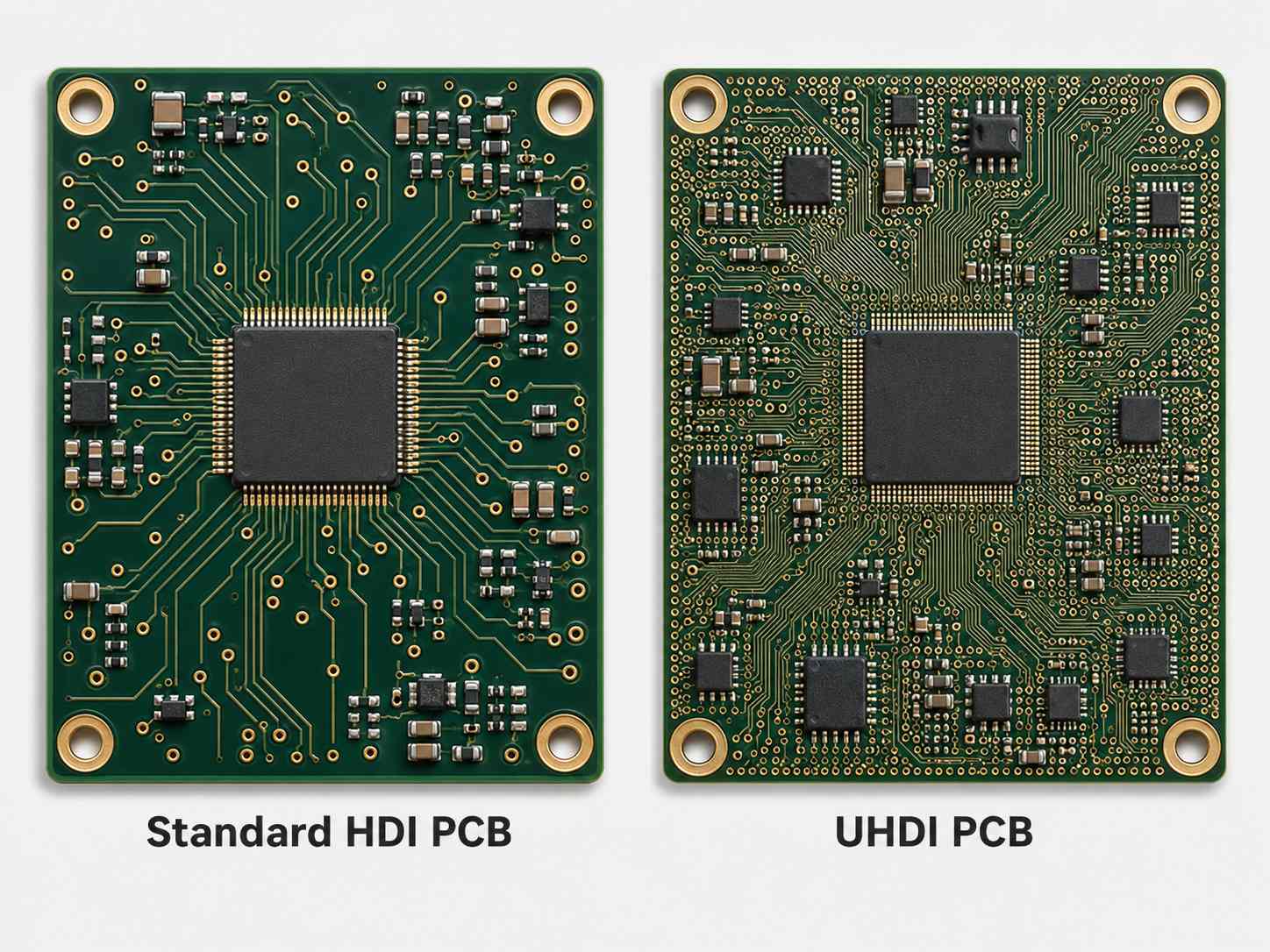
How Is UHDI PCB Fabrication Different from Standard HDI PCB?

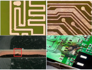
UHDI PCB fabrication goes beyond standard HDI PCB manufacturing. It pushes line width, spacing, microvia size, pad density, and layer build-up control closer to the limits of PCB process capability.

Key differences include:

  • Finer line and spacing
    • UHDI requires tighter etching and imaging control.
    • Dense BGA or RF component breakout may need finer routing channels.
  • Smaller microvias
    • UHDI boards rely heavily on laser microvias.
    • Stacked or staggered microvia structures must be reviewed for reliability.
  • Higher interconnect density
    • More routing can fit into a smaller board area.
    • This is useful for compact RF modules, high-speed computing, and advanced communication hardware.
  • More sensitive stack-up control
    • Thin dielectric layers may be needed.
    • Impedance targets become more sensitive to small fabrication variations.
  • More demanding inspection
    • Fine traces, microvias, and via-in-pad features need close process control.
    • AOI, electrical testing, impedance testing, and microsection review may be required depending on the project.

For EBest Circuit (Best Technology), UHDI PCB fabrication starts with file review. Before production, we check whether the line/space, microvia structure, via filling, stack-up, copper thickness, surface finish, and impedance requirements are practical for manufacturing.

UHDI PCB

Why Do 80 GHz RF Applications Need UHDI PCB Fabrication?

An 80 GHz PCB project combines two difficult requirements: high-frequency signal performance and high-density interconnection. At this frequency range, the PCB material and fabrication process can influence insertion loss, impedance stability, phase behavior, and connector or component launch performance.

UHDI fabrication may be needed in 80 GHz RF applications because:

  • Signal paths must be compact
    • Shorter interconnects can help reduce unwanted parasitic effects.
    • Dense routing helps fit RF functions into a smaller module.
  • Impedance control becomes more sensitive
    • Trace width, copper thickness, dielectric thickness, and reference layer spacing must be controlled.
    • Even small stack-up changes may affect impedance.
  • Material loss matters
    • Standard FR4 is usually not suitable for high-frequency RF boards.
    • Low-loss laminates such as Megtron 6 or Rogers materials are often considered for high-speed and RF applications.
  • Microvia and via-in-pad structures may be required
    • High-density RF packages often need compact fanout.
    • Microvias and via-in-pad help reduce routing distance and save board area.
  • Manufacturing tolerance affects performance
    • Line width, copper profile, dielectric thickness, and surface finish need to be reviewed together.
    • The board should be fabricated according to the approved stack-up and impedance requirements.

EBest Circuit (Best Technology) does not provide RF circuit design or simulation. Our role is to support manufacturability review, material feasibility review, stack-up feedback, impedance control, PCB fabrication, assembly, and testing based on customer-provided files.

Which Materials Are Suitable for UHDI PCBs: Megtron 6, Rogers, or Other Low-Loss Laminates?

UHDI PCB material should be selected according to frequency, signal type, stack-up, board thickness, copper profile, assembly process, and cost target. For an 80 GHz board, material choice becomes a major decision.

Common material options include:

  • Megtron 6
    • Often used for high-speed and low-loss applications.
    • Suitable for many high-speed digital and certain RF-related designs.
    • Needs stack-up and impedance review before production.
  • Rogers materials
    • Common in RF, microwave, antenna, and millimeter-wave applications.
    • Often selected when RF loss, Dk stability, and frequency performance are critical.
    • Material grade should match the customer’s RF requirement.
  • Other low-loss laminates
    • Isola, Taconic, Nelco, Panasonic, and other material systems may be considered depending on performance, availability, and cost.
    • Substitution should not be made without customer approval.

Material selection affects:

  • Dk and Df
  • Insertion loss
  • Impedance control
  • Copper roughness
  • Lamination behavior
  • Board thickness
  • Microvia reliability
  • Lead time and cost

For a UHDI PCB working at 80 GHz, EBest Circuit (Best Technology) reviews material availability, stack-up feasibility, copper thickness, dielectric thickness, surface finish, and manufacturing tolerance before quotation. If the customer specifies Megtron 6 or Rogers, we treat that as a key technical requirement rather than a casual material preference.

How Does EBest Circuit (Best Technology) Support Preliminary Stack-Up Review for UHDI PCB?

A preliminary stack-up is often needed before final impedance matching, especially for high-frequency UHDI PCBs. However, stack-up support should be handled carefully. EBest Circuit (Best Technology) can support stack-up review and manufacturability feedback, but we do not replace the customer’s RF design, simulation, or final impedance modeling.

Our preliminary stack-up support may include:

  • Material feasibility review
    • Check whether the requested material is suitable and available.
    • Review Megtron 6, Rogers, or other low-loss laminate options.
  • Dielectric thickness feedback
    • Review whether proposed dielectric thicknesses are manufacturable.
    • Check whether thin build-up layers match microvia requirements.
  • Copper thickness review
    • Check whether copper thickness supports fine line fabrication.
    • Review inner and outer copper requirements.
  • Impedance manufacturability feedback
    • Review whether target impedance values are practical with the proposed stack-up.
    • Support controlled impedance production according to approved requirements.
  • Microvia structure review
    • Check blind vias, buried vias, stacked vias, staggered vias, and via-in-pad.
    • Review via filling or plating requirements.
  • Fabrication tolerance review
    • Evaluate how line width, spacing, copper thickness, and dielectric tolerance may affect production.

What customers should provide if available:

  • Target impedance values
  • Operating frequency
  • Material preference
  • Layer count
  • Board thickness target
  • Controlled layers
  • Differential pair requirements
  • Copper weight
  • Via structure
  • RF connector or launch area notes

The final stack-up should be confirmed by the customer’s engineering team after impedance modeling and product-level review. EBest Circuit (Best Technology) helps make sure the stack-up is practical for PCB manufacturing.

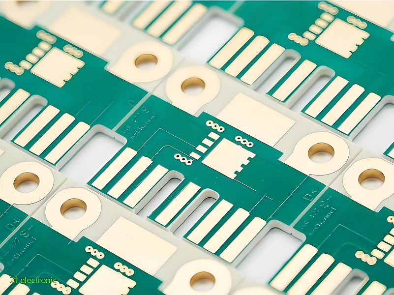
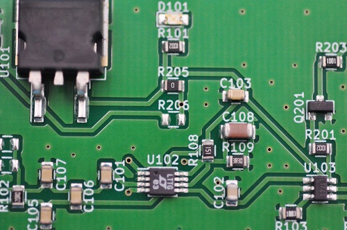
What UHDI PCB Fabrication Capabilities Does EBest Circuit (Best Technology) Offer?

For UHDI PCB projects, customers should not only ask whether a supplier can make HDI boards. The better question is whether the supplier can support the specific combination of fine routing, microvias, low-loss material, controlled impedance, stack-up review, testing, and prototype-to-volume production.

EBest Circuit (Best Technology) supports UHDI and advanced HDI projects with the following manufacturing-related capabilities:

Capability AreaEBest Circuit (Best Technology) Support
Fine line/spaceAdvanced HDI/UHDI feature review
Laser microviasMicrovia and laser via process support
HDI structuresBlind vias, buried vias, stacked/staggered vias
Via-in-padVia filling and plating review
Layer countMultilayer and high-layer-count PCB support
MaterialsMegtron, Rogers, high-Tg FR4, and other low-loss materials
ImpedanceControlled impedance review and testing support
Surface finishENIG, ENEPIG, immersion silver, hard gold, and project-based options
InspectionAOI, electrical test, impedance test, X-ray when required
Engineering supportDFM review and PCB layout manufacturability feedback

Key process points we review before production:

  • Minimum line width and spacing
  • Laser via diameter and aspect ratio
  • Annular ring and capture pad
  • Via-in-pad filling requirement
  • Copper thickness
  • Dielectric thickness
  • Controlled impedance tolerance
  • Solder mask registration
  • RF launch area manufacturability
  • Board flatness and dimensional control
  • Prototype and volume production consistency

For high-frequency UHDI boards, process capability should be reviewed before pricing is finalized. A quotation without material, stack-up, impedance, and via structure review may look fast, but it may not be reliable.

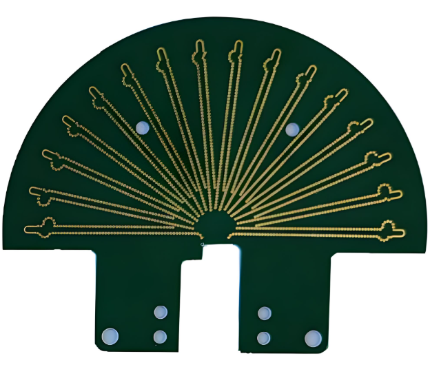
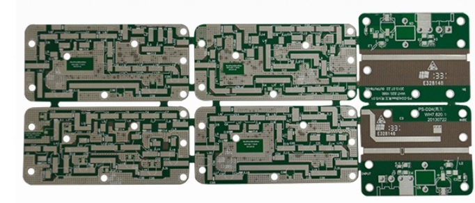
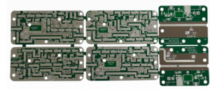
Case Study: UHDI PCB Prototype Review for an 80 GHz Board

A customer contacted EBest Circuit (Best Technology) for a UHDI printed circuit board intended to operate at 80 GHz.

This case is a strong example of why UHDI PCB quotation should start with engineering review, not just price calculation.

Project Overview

  • Board type: UHDI PCB
  • Application: 80 GHz RF operation
  • Material requirement: Megtron 6 or Rogers
  • Quote scope: prototype, 100 units, 1000 units
  • Customer need: unit price, lead time, stack-up support, impedance matching support
  • Files provided: Gerber files and technical requirements

Customer Requirements

  • Prototype fabrication price
  • Price breaks for 100 units and 1000 units
  • Typical lead time
  • Confirmation of any missing information
  • Preliminary or final stack-up structure
  • Material support for Megtron 6 or Rogers
  • Manufacturability review for high-frequency UHDI fabrication

EBest Circuit (Best Technology)’s Review Focus

For this type of UHDI PCB, our engineering review focuses on:

  • Material availability and suitability
  • Stack-up manufacturability
  • Controlled impedance feasibility
  • Fine line/space capability
  • Laser microvia structure
  • Via-in-pad and filled via requirements
  • Surface finish selection
  • RF launch and connector area manufacturability
  • Prototype and volume consistency
  • Testing and report requirements

Project Value

This case shows that an 80 GHz UHDI PCB cannot be quoted like a standard FR4 prototype. The supplier must review material, stack-up, impedance, microvia structure, and fabrication tolerance before confirming cost and lead time.

EBest Circuit (Best Technology) helps customers move from early quotation to manufacturability review by checking the files first, clarifying missing details, and supporting prototype-to-volume evaluation based on the same technical baseline.

What Files Are Needed for a UHDI PCB Prototype and Volume Quote?

Customers do not need to prepare a perfect file package before contacting EBest Circuit (Best Technology). You can send available files first. Missing details can be clarified during engineering review.

For an initial UHDI PCB quote, these files are helpful:

  • Gerber files
  • Drill files
  • Board size
  • Layer count
  • Quantity
  • Material requirement
  • Board thickness target
  • PCB only or PCBA requirement

For a more accurate UHDI PCB fabrication quote, please add if available:

  • Stack-up
  • Impedance table
  • Controlled impedance tolerance
  • Copper thickness
  • Surface finish
  • Via structure
  • Via filling requirement
  • RF connector or launch area notes
  • Testing requirements
  • Report requirements

For prototype and volume pricing, it is useful to provide:

  • Prototype quantity
  • 100-unit requirement
  • 1000-unit requirement
  • Target lead time
  • Standard or expedited delivery request
  • Any expected production ramp plan

For PCBA quotation, please add:

  • BOM
  • Pick and place file
  • Assembly drawing
  • Component polarity notes
  • BGA or fine-pitch component information
  • Testing requirement, if any

Cost and lead time are affected by:

  • Material type
  • Material availability
  • Layer count
  • Board size
  • UHDI line/space
  • Laser via structure
  • Via-in-pad and filling
  • Impedance tolerance
  • Surface finish
  • Testing requirements
  • Quantity and production stage

To start a review, send your available files and technical notes to sales@bestpcbs.com. EBest Circuit (Best Technology) will review the project and advise what additional details are needed before quotation.

Why Choose EBest Circuit (Best Technology) for UHDI PCB Fabrication?

Choosing a UHDI PCB manufacturer is not only about finding a supplier that can quote quickly. For 80 GHz RF applications, customers need a manufacturer that can review the board from a manufacturability, material, impedance, and assembly perspective.

Why customers work with EBest Circuit (Best Technology):

  • Engineer-oriented support
    • DFM review before production
    • PCB layout manufacturability feedback
    • Stack-up manufacturability review
    • Engineering questions before manufacturing
  • High-frequency material experience
    • Megtron material review
    • Rogers material review
    • Low-loss laminate options
    • Material availability feedback
  • Advanced HDI/UHDI capability
    • Fine line/space review
    • Laser microvias
    • Blind and buried vias
    • Via-in-pad
    • Filled via process review
  • Controlled impedance support
    • Preliminary stack-up feedback
    • Impedance manufacturability review
    • Impedance test support when required
  • Prototype-to-volume workflow
    • Prototype fabrication
    • 100-unit and 1000-unit evaluation
    • Volume production review
    • Production documentation support
  • One-stop PCB service
    • PCB fabrication
    • Component sourcing
    • PCBA assembly
    • AOI inspection
    • X-ray inspection when required
    • Testing support based on customer requirements

EBest Circuit (Best Technology) is suitable for customers who need more than a bare-board quote. We help engineering teams confirm whether the UHDI PCB can be manufactured, assembled, tested, and scaled from prototype to production.

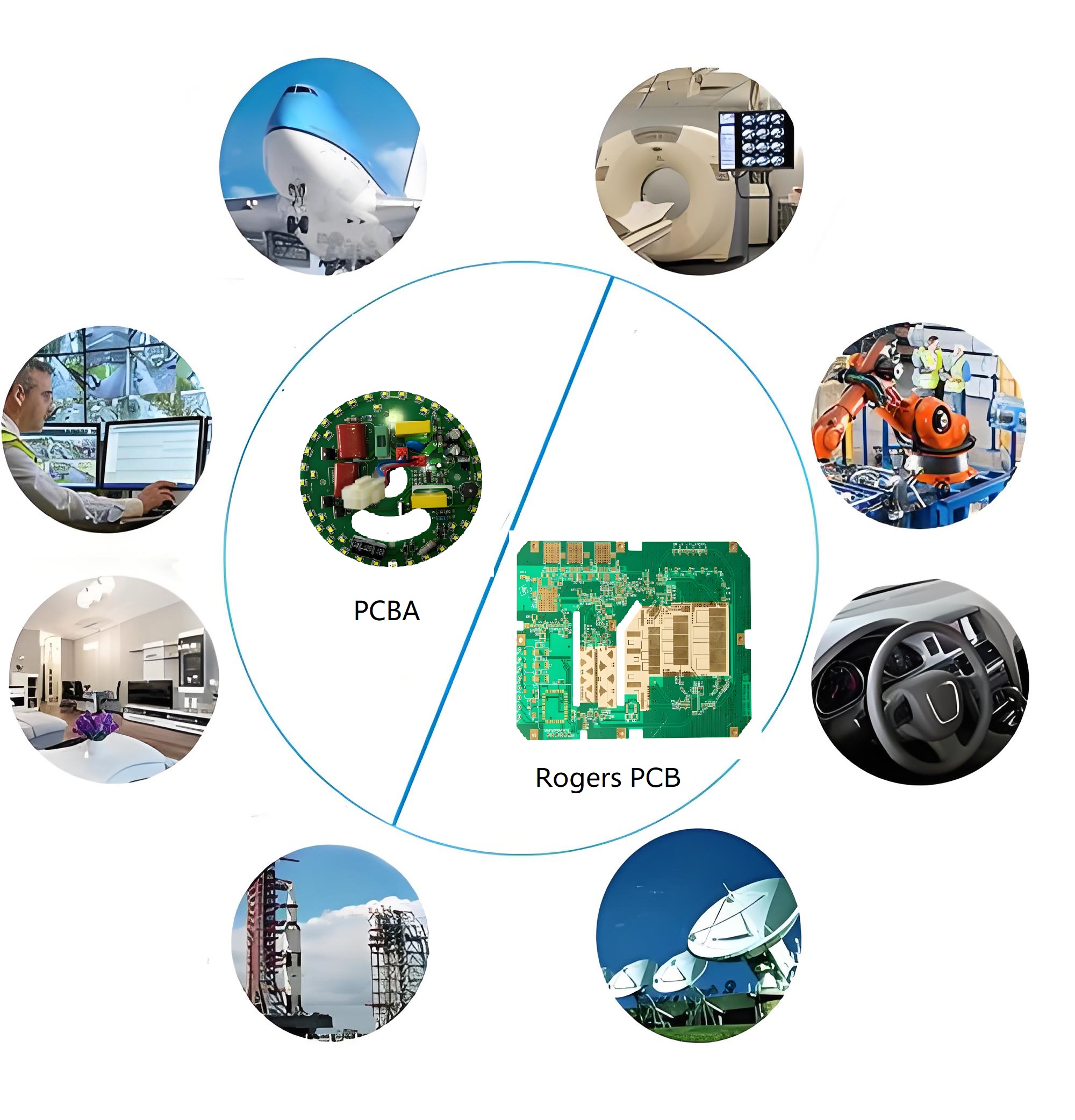
For UHDI PCB fabrication, 80 GHz RF boards, Megtron 6 PCB, Rogers PCB, or prototype-to-volume quotation, contact sales@bestpcbs.com.

UHDI PCB

FAQs About UHDI PCB

What is a UHDI PCB?
A UHDI PCB is an ultra high-density interconnect printed circuit board using very fine routing features, microvias, via-in-pad, and dense layer structures to support compact and high-performance electronics.

How is UHDI PCB different from HDI PCB?
UHDI PCB pushes HDI technology further with finer line/space, smaller microvias, higher routing density, and tighter fabrication control. It is often used when standard HDI is not dense enough.

Can UHDI PCB be used for 80 GHz applications?
Yes, but the project must combine UHDI fabrication capability with suitable RF materials, controlled impedance, stack-up review, and high-frequency manufacturability checks.

Is Megtron 6 suitable for UHDI PCB fabrication?
Megtron 6 can be suitable for certain high-speed and low-loss applications. For 80 GHz projects, material selection should be reviewed together with frequency, stack-up, impedance, copper profile, and customer requirements.

Can Rogers materials be used for UHDI RF boards?
Yes. Rogers materials are commonly used in RF and microwave PCB applications. The exact grade should be selected based on frequency, Dk/Df, stack-up, thickness, and RF performance requirements.

Can EBest Circuit (Best Technology) provide preliminary stack-up support?
Yes. EBest Circuit (Best Technology) can provide preliminary stack-up review and manufacturability feedback based on customer-provided requirements. Final design validation and RF simulation should be confirmed by the customer’s engineering team.

What files are needed for a UHDI PCB quote?
Gerber files, drill files, board size, layer count, material requirement, quantity, and board thickness target are helpful for initial review. Stack-up, impedance table, via structure, copper thickness, and testing requirements help provide a more accurate quote.

Can UHDI PCB prototypes and volume orders be quoted together?
Yes. Prototype, 100-unit, and 1000-unit quantities can be reviewed together. This helps customers understand price breaks, lead time, and production scalability.

Does EBest Circuit (Best Technology) support UHDI PCB assembly?
Yes. EBest Circuit (Best Technology) supports PCB fabrication and PCBA assembly, including component sourcing, SMT assembly, AOI, X-ray inspection when required, and testing support based on customer files.

How can I start a UHDI PCB fabrication project?
Send your available Gerber files, drill files, technical notes, material requirement, stack-up information, and quantity request to sales@bestpcbs.com. EBest Circuit (Best Technology) will review the project and confirm what additional information is needed.

You may also like

Rogers RO3003 Laminate Datasheet Detailed Explaination
Monday, December 8th, 2025

RO3003 is widely used across RF and microwave PCB because it offers stable electrical behavior, low loss, and smooth processing on modern PCB lines. Engineers often choose this laminate when they need predictable impedance, steady phase response, and strong thermal performance at high frequencies. Below is a comprehensive, fabrication-level RO3003 datasheet, covering electrical, mechanical, thermal, chemical, processing, and reliability properties.

Rogers RO3003 Laminate Datasheet Detailed Explaination

Rogers RO3003 Laminate Datasheet

Rogers RO3003™ Electrical Properties

ParameterConditionTypical ValueNotes
Dielectric Constant (Dk)10 GHz (IPC-TM-650 2.5.5.5)3.00 ± 0.04Very stable across temperature and frequency
Dielectric Constant (Dk)2.5 GHz3.01Suitable for wideband RF
Dissipation Factor (Df)10 GHz0.0010Extremely low loss
Dissipation Factor (Df)2.5 GHz0.0009Excellent for mmWave
Volume Resistivity23°C / 50% RH1.7 × 10Âč⁰ MΩ·cmHigh electrical insulation
Surface Resistivity23°C / 50% RH5.7 × 10âč MΩStable in damp conditions
Electric Strength0.5 mm thickness35 kV/mmStrong dielectric barrier
Impedance Stability-40°C to +85°C±1.3%Very stable for antenna structures
Dk Temperature Coefficient (TCDk)-40 to +85°C-3 ppm/°CVery low drift

RO3003 is chosen often for 77 GHz radar, 24 GHz radar, and mmWave antennas because of these stable dielectric properties.

RO3003™ Material Thermal Properties

ParameterTypical ValueNotes
Thermal Conductivity0.5 W/m·KHigher than FR4
Usable Temperature Range-55°C to +150°CSuitable for automotive radar
Dimensional Stability (X/Y)0.2–0.3%Strong laminate stability
Coefficient of Thermal Expansion (CTE) – X17 ppm/°CMatches copper closely
CTE – Y17 ppm/°CHelps reduce expansion stress
CTE – Z24 ppm/°CCritical for microvias
Thermal Decomposition Temp (Td)> 400°CMuch higher than FR4
Thermal Stress288°C / 10 secNo delamination
Specific Heat1.0 J/g-KSupports stable power handling

The matched X/Y CTE and moderate Z-axis CTE improve reliability in multi-layer RF boards, QFN modules, and BGA transitions.

RO3003™ Mechanical Properties

ParameterConditionTypical Value
Tensile Modulus (MD)23°C18,000 MPa
Tensile Modulus (CD)23°C17,500 MPa
Flexural Strength23°C340 MPa
Peel Strength1 oz Cu, after thermal aging8.0 lb/in
Density—2.1 g/cm³
Hardness (Shore D)—74
Moisture Absorption48h @ 50°C water0.02%

Low moisture absorption is one of the main reasons designers choose Ro3003 laminate for outdoor and long-range radio systems.

RO3003™ Chemical & Environmental Properties

PropertyTypical Value
FlammabilityUL 94 V-0
Fungus ResistancePass
Copper Corrosion TestPass
Water Absorption0.02%
RoHSCompliant
Lead-Free AssemblyFully supported

The laminate performs well in harsh environments such as marine radar, industrial sensors, and automotive radar systems.

RO3003™ Thickness Availability

Standard ThicknessInchesMilNotes
0.127 mm0.0050″5 milVery common for antennas
0.203 mm0.0080″8 milGood for compact RF paths
0.254 mm0.0100″10 milLNA/PA front-end boards
0.508 mm0.0200″20 milMany GPS modules
0.762 mm0.0300″30 milLower insertion loss
1.524 mm0.0600″60 milLarge antennas or radar

Copper foil options include:

Copper TypeStandard WeightNotes
ED Copperœ oz, 1 ozBest for general RF
Reverse-Treat Copper (RTF)œ oz, 1 ozBetter for low-loss designs
Rolled CopperLimitedUsed for bending applications

RO3003™ Available Panel Sizes

Panel SizeNotes
12″ × 18″Most common
18″ × 24″Higher utilization
24″ × 36″For mass production
Custom CutsBy manufacturer

Panel selection strongly affects Rogers 3003 price because utilization changes final cost.

RO3003™ Impedance Control Data

Line TypeResult on 10 mil RO3003Notes
50 Ω Microstrip~23 mil widthTypical, depends on copper
75 Ω Microstrip~12 mil widthUsed in satellite links
100 Ω Differential Pair8–10 mil / 8–10 mil spacingDepends on copper thickness
90 Ω Diff Pair10–12 milCommon in RF front ends

For mmWave (60–86 GHz), designers often use:

FeatureTypical Value
Via Stub Target< 6 mil
CPWG Gap6–8 mil
BendsAvoid sharp angles

RO3003™ Reliability Properties

TestResult
Thermal CyclingExcellent stability
IST TestLow via fatigue
PTH ReliabilityStable with standard processes
Solder FloatNo blistering
High-Temp ExposureNo resin cracking
Multi-Reflow TestStable after 3× lead-free reflow

RO3003 is widely used in 77 GHz automotive radar because it withstands large temperature swings without drift.

RO3003™ Comparison Against Other Rogers Materials

ParameterRO3003RO4003CRO4350B
Dk3.003.383.48
Df0.00100.00270.0037
Moisture Absorption0.02%0.04%0.06%
Thermal Conductivity0.5 W/m·K0.3 W/m·K0.6 W/m·K
Dimensional StabilityHighMediumHigh
Fabrication DifficultyLowVery lowLow
CostHighestLowestMedium
Best ForRadar, mmWaveGeneral RFTelecom, WiFi, RF modules

RO3003™ Material Stack-Up Examples

  • 1- Layer RF Antenna Stack-Up
LayerMaterial
Top Copper18 ÎŒm RTF
DielectricRO3003 10 mil
Ground Copper18 ÎŒm RTF
  • 2-Layer Balanced RF Module
LayerMaterial
Signal Layerœ oz copper
RO3003 Core20 mil
Ground Layer1 oz copper
  • Hybrid RF + Digital Stack-Up
LayerMaterial
Top CopperRF traces
RO300310 mil
Adhesive Layer—
FR4 PrepregStandard
FR4 CoreDigital circuits
Bottom CopperGround / digital signals

If your next RF project involves RO3003 or other high-frequency laminates, our engineering team is ready to assist with simulations, stack-up proposals, prototype runs, and volume builds. You are welcome to contact EBest Circuit (Best Technology) for professional guidance and fast support as you move from concept to production.

Our teams support RF designers from the early stack-up stage through final production with careful engineering review, material guidance, and precise process control. Every PCB moves through certified systems, including ISO9001, ISO13485, IATF16949, and AS9100D, which gives customers confidence in long-term reliability.

You may also like

Rogers PCBs – The Ideal Choice for High-Speed Communication
Saturday, July 12th, 2025

In EBest Circuit (Best Technology), the printed circuit Board manufacturing, particularly in high-frequency and high-speed signal transmission applications, Rogers Corporation’s PCB materials have become the go-to choice for our engineers. Rogers specializes in producing high-performance, highly reliable circuit board materials that find extensive use in wireless communications, automotive radar, satellite communication, and more. This blog post explores the unique advantages of Rogers PCBs and their significance in the international market.

Rogers PCBs – The Ideal Choice for High-Speed Communication

What is Rogers PCB?

Rogers PCBs are renowned for their exceptional electrical performance. Compared to traditional FR-4 materials, Rogers materials offer a lower dissipation factor (Df), meaning they can maintain signal integrity at higher frequencies with reduced energy loss. This is critical for applications requiring precise data transmission such as 5G communications and millimeter-wave radars.

Rogers materials exhibit outstanding thermal stability. In high-temperature environments, these materials retain dimensional stability and mechanical strength, ensuring the reliability of PCBs under extreme conditions. For devices that need to operate stably over long periods, such as base stations or satellite communication equipment, this feature is especially important. Here is a comparison between Rogers materials and FR4.

PropertyRogers MaterialFR4 Material
Dielectric Constant (Dk)Low and stable (e.g. 2.2 – 3.5)Higher and less stable (around 4.3 – 4.8)
Loss Tangent (Df)Very low (as low as 0.0009)Higher (typically ~0.02)
Signal LossMinimal, ideal for high-frequency applicationsMore signal loss at high frequencies
Frequency PerformanceExcellent at RF/microwave frequencies (GHz range)Poor performance above 1 GHz
Thermal StabilityExcellent (low Dk variation with temperature)Moderate
Thermal ConductivityHigher (improves heat dissipation)Lower
CostHighLow
Material CompositionCeramic-filled or hydrocarbon-based laminatesWoven glass epoxy resin
ApplicationRF, microwave, satellite, aerospace, radar, 5GConsumer electronics, computers, industrial devices
Moisture AbsorptionVery lowHigher
Impedance ControlBetter and more predictableLess accurate
ManufacturabilityRequires experienced processing (different drilling etc.)Easy to process using standard PCB methods

Moreover, Rogers offers a range of materials with different characteristics to cater to various application needs. From low-loss to ultra-high-frequency applications, customers can choose the most suitable material based on their specific requirements. This not only enhances design flexibility but also provides more solutions to address complex engineering challenges.

In the context of globalization, competition in the international market has intensified. Utilizing Rogers PCB materials not only elevates the technical content and competitiveness of products but also offers customers a superior service experience. With the widespread adoption of 5G technology and the development of the Internet of Things (IoT), the demand for high-performance PCBs will continue to grow, making Rogers a leader in this field.

Advantages of Rogers PCB

1. Superior High-Frequency Performance

Rogers PCBs offer excellent electrical performance at high frequencies. Their stable dielectric constant and low loss tangent minimize signal loss and dispersion, which is critical for RF and microwave applications.

2. Low Dielectric Loss

Rogers materials have very low Df (dissipation factor), reducing power loss during signal transmission. This makes them highly efficient for high-speed, high-frequency signal paths.

3. Excellent Thermal Management

Rogers laminates have better thermal conductivity compared to standard FR4, allowing for more efficient heat dissipation. This helps maintain performance in demanding temperature environments.

4. Stable Electrical Properties

Their dielectric constant remains consistent over a wide range of temperatures and frequencies, enabling precise impedance control and signal integrity in advanced circuit designs.

5. Low Moisture Absorption

Rogers materials absorb less moisture than FR4, making them reliable for outdoor, aerospace, or high-humidity environments.

6. Better Reliability for Harsh Environments

With high temperature resistance and chemical stability, Rogers PCBs perform well in aerospace, military, and industrial applications where standard FR4 may fail.

Rogers PCBs – The Ideal Choice for High-Speed Communication

Applications of Rogers PCB

1. RF and Microwave Circuits

Rogers PCBs are widely used in radio frequency (RF) and microwave communication systems, including antenna arrays, radar modules, and RF amplifiers.

2. 5G Infrastructure

Due to their low signal loss and excellent high-frequency characteristics, Rogers boards are ideal for 5G base stations, antennas, and network hardware.

3. Aerospace and Defense Systems

In aviation, satellites, and military electronics, Rogers PCBs provide the precision and durability needed for mission-critical communication and control systems.

4. Automotive Radar and ADAS

Modern vehicles use Rogers-based PCBs in advanced driver assistance systems (ADAS), radar sensors, and collision avoidance modules for reliable performance under extreme conditions.

5. Medical Imaging and Equipment

Rogers boards are used in MRI machines, RF ablation devices, and other diagnostic tools where consistent signal performance is crucial.

6. High-Speed Digital Circuits

In computing and telecommunications, Rogers materials support high-speed signal integrity for backplanes, routers, and high-frequency data transmission boards.

Applications of Rogers PCB

Conclusion

Rogers PCBs stand out globally due to their outstanding performance and broad applicability. Whether developing new communication devices or improving existing systems, choosing Rogers is a wise decision. Their commitment to innovation ensures they remain at the forefront of technological advancement, providing unparalleled solutions for tomorrow’s electronic challenges.

Best Tech is a very professional manufacturer in printed circuit board. If you are interesting to know more information for Rogers PCB and other high-speed signal transmission application for printed circuit board, please come to contact us at any time.

You may also like

Rogers RT Duroid 5880 | High Frequency Rogers RO5880 PCB Manufacturer
Wednesday, October 16th, 2024

What substrate is Rogers RT Duroid 5880?

Rogers RT Duroid 5880 is a high-frequency laminate specifically designed for applications where precision and low signal loss are critical. The substrate is a composite material known for its excellent performance in RF and microwave circuits. It uses a PTFE (polytetrafluoroethylene) base reinforced with glass microfibers.

The use of glass microfiber ensures the material is durable but lightweight, making it suitable for applications in which weight is a factor. Its composition is perfect for projects where high-frequency signals are involved. From defense systems to automotive radar, RT Duroid 5880 is a reliable choice. It has become the go-to substrate for engineers and designers looking for efficiency, precision, and durability.

Rogers RT Duroid 5880 | High Frequency Rogers RO5880 PCB Manufacturer

Composition of Rogers RT/duroid 5880

RT Duroid 5880 is composed of PTFE (polytetrafluoroethylene) combined with glass microfiber. PTFE provides a low dissipation factor, which reduces signal loss. This is important for maintaining high performance in RF and microwave applications. Glass microfiber reinforces the material, make it stronger without adding unnecessary weight. The composition also includes copper cladding, which is typically laminated on both sides. The copper layer helps with conductivity, ensuring signals travel efficiently across the board.

The unique combination of PTFE and glass microfiber gives RT Duroid 5880 its excellent mechanical stability. It also minimizes the effect of temperature changes, which is critical for high-frequency circuits. As a result, the material can handle extreme temperatures without affecting the performance of the PCB.

RT/duroid 5880 Specifications

The following table highlights the important specifications of Rogers RT Duroid 5880. These specs reflect the high performance of RT Duroid 5880 for complex RF and microwave tasks.

PropertyValue
Dielectric Constant (Dk)2.20 (±0.02)
Dissipation Factor (Df)0.0004 (measured at 10 GHz)
Thermal Conductivity0.20 W/m/K
Operating Temperature Range-55°C to +150°C
Water Absorption0.02%
Volume Resistivity1.7 x 10^9 MΩ·cm (minimum)
Surface Resistivity1.4 x 10^8 MΩ (minimum)
Coefficient of Thermal Expansion (CTE)46 ppm/°C (in X-Y axis)
Tensile Strength10.3 MPa
FlammabilityUL 94 V-0
Peel Strength5.0 N/mm (after soldering)

RT/duroid 5880 Thickness

RT Duroid 5880 comes in various thicknesses. Engineers can choose the right thickness depending on their project’s needs. Rogers RT/duroid 5880 laminate is commercially available in sheet stock and roll stock forms in a range of thicknesses. Here’s a list of the standard thicknesses available:

Available sheet sizes:

  • 304.8 x 457.2 mm
  • 457.2 x 609.6 mm
  • 609.6 x 914.4 mm

Standard thickness:

  • 0.127 mm (5 mils)
  • 0.254 mm (10 mils)
  • 0.381 mm (15 mils)
  • 0.508 mm (20 mils)
  • 0.787 mm (31 mils)
  • 1.524 mm (60 mils)
  • 3.175 mm (125 mils)

Available roll widths:

  • 304.8 mm
  • 609.6 mm
  • 1219.2 mm
  • Standard roll length: 76.2 meters
  • Thickness range: 0.127 mm to 1.575 mm ​

RO5880 RF PCB Advantages

Rogers RT Duroid 5880 has a lot of strengths when used in RF and microwave PCB projects:

  • Minimal Signal Loss

With a low dissipation factor of 0.0004, it reduces signal loss, which is very helpful for high-frequency systems like radar or satellite communications.

  • Strong Stability

It holds up well under temperature changes and in humid environments, keeping circuits running smoothly even in tough conditions.

  • Reliable Electrical Properties

The dielectric constant of 2.20 remains stable over a range of frequencies. This helps keep circuits working consistently without interference or signal issues.

  • Heat Tolerance

It withstands heat up to 150°C, making it a good choice for systems that need to handle higher temperatures.

  • Low Moisture Absorption

With only 0.02% water absorption, the material works well in damp environments. Outdoor systems like antennas benefit from this.

  • Ease of Manufacturing

The material is easy to work with during production, which keeps costs lower and speeds up manufacturing.

  • Chemical Resistance

The PTFE base resists damage from chemicals and solvents, making the material last longer in harsh environments like aerospace and industrial applications.

Typical Applications of High-Frequency PCB

High-frequency PCBs built with Rogers RT Duroid 5880 serve important roles across many industries:

  • Aerospace – used in radar, satellite, and navigation systems, RT Duroid 5880 supports reliable communication and tracking, even in high-pressure environments.
  • Telecommunications – in mobile networks, base stations, and antennas, high-frequency PCBs help maintain clear and fast data transmission, supporting the backbone of communication systems.
  • Medical Devices – MRI machines, wireless health monitors, and other equipment use high-frequency PCBs to keep medical data accurate and systems working seamlessly.
  • Defense – communication gear, and electronic warfare systems.
  • Automotive Systems – advanced driver assistance systems (ADAS) and vehicle radar depend on high-frequency PCBs for real-time data, making roads safer for everyone.
  • Satellite Communication – RT Duroid 5880 is frequently used in satellite systems where strong signal transmission over long distances is crucial for communication networks.

Common-Used High Frequency PCB Materials in EBest Circuit (Best Technology)

At EBest Circuit (Best Technology), we use a range of top-quality materials for high-frequency PCBs, depending on the project’s needs. Some of the most popular materials include:

Material       Dielectric Constant (Dk)      Loss Tangent (Df)       Key Features  
Rogers RO4003C3.380.0027Low loss, excellent thermal stability, ideal for RF applications.
Rogers RO43503.480.0043Low loss, high thermal conductivity, suitable for microwave applications.  
RT/Duroid RO58802.940.0037Very low loss, excellent performance at high frequencies, good for multilayer designs.  
N4000-133.00.009Good thermal stability, low moisture absorption, designed for high-frequency applications.
Taconic RF-60A6.150.0027High dielectric constant, low loss, suitable for low-loss RF and microwave applications.  

Each material brings different strengths for specific applications, giving you the best options for your project.

Discuss Your High Frequency PCB Project with Us Today

If you have a high-frequency PCB project in mind, reach out to us. We’re experienced in creating high-quality PCBs that meet your exact specifications. Whether you need RF, microwave, or other types of high-frequency boards, we’ll make sure your project runs smoothly. Contact us at sales@www.bestpcbs.com today, and we’ll help you turn your plans into reality.

You may also like

High Frequency PCB & High Frequency PCB Prototype
Friday, September 20th, 2024

What is High-Frequency PCBs?

What is High-Frequency PCBs? High frequency PCBs are specifically designed to operate at frequencies typically above 1GHz. These circuit boards play a crucial role in modern communication systems like satellite communications, radar, and wireless networks. The materials used in high-frequency PCBs are different from those in standard PCBs. While standard PCBs use FR4 material, high-frequency PCBs often require specialized materials like PTFE (Teflon) or Rogers material to reduce signal loss and improve overall performance.

The growing need for faster and more reliable communication across industries makes high-frequency PCBs essential for creating cutting-edge devices.

High Frequency PCB Materials

Click here to download Raw Materials of RF PCB.

Advantages of High Frequency PCB

  • Faster signal transmission
  • Better signal integrity
  • Enhanced thermal management
  • Low electromagnetic interference (EMI)
  • Application in emerging technologies
  • Improved precision in high-speed applications

What is the Frequency Limit for FR4 PCB?

FR4 is the most widely used material in standard PCBs due to its affordability and adequate performance for general applications. However, when it comes to high-frequency operations, FR4 has its limitations. The material can handle frequencies up to about 1GHz, but beyond this range, its performance starts to degrade significantly. High-frequency signals experience increased signal loss, dielectric losses, and electromagnetic interference (EMI) due to FR4’s higher dielectric constant (around 4.5) and poor thermal properties.

The limitations make FR4 unsuitable for more advanced applications like high-speed telecommunications, radar systems, and modern wireless technologies where signals operate in the gigahertz range. When designing PCBs that require frequencies beyond 1GHz, alternative materials like PTFE (Teflon) or Rogers laminates are recommended to maintain signal integrity and reduce losses.

How Do You Make High-Frequency PCB?

Creating a high-frequency PCB involves a few additional considerations compared to standard PCB designs. First, the choice of materials is critical. PTFE, Rogers, and other high-performance laminates are commonly used to ensure the PCB can handle high-frequency signals. Next, the board’s thickness, trace width, and layout need to be carefully calculated to avoid impedance issues. The key process including:

1. Material Selection

The first step is choosing materials that can handle high-frequency signals. Materials like PTFE, Rogers, or ceramic substrates are commonly used because they have lower dielectric constants, low dissipation factors, and better thermal stability. These materials ensure minimal signal degradation.

2. Controlled Impedance

High-frequency signals are sensitive to variations in impedance. Controlled impedance design ensures that the trace impedance matches the signal’s requirements, preventing reflection and signal distortion. This involves calculating the width and spacing of the traces and ensuring consistent dielectric properties across layers.

3. Multi-layer PCB

Multi-layer boards are often necessary for high-frequency applications to separate signals and reduce cross-talk. Ground planes are typically added to lower electromagnetic interference (EMI) and provide better signal grounding.

4. Short and Direct Signal Paths

Keeping signal paths as short as possible helps minimize signal loss and prevents unwanted interference. Traces that are too long or involve sharp bends can introduce delay and noise.

5. Shielding

In some cases, shielding techniques can be employed to prevent interference from other electronic components. This can include grounded planes, copper shields, or even encapsulating certain areas of the PCB.

High-frequency PCB design often requires sophisticated simulation tools. Software such as Ansys or Altium Designer helps predict how signals will behave on the board, allowing for adjustments to be made before fabrication.

What is the Highest RF Frequency?

In communication circuits, radio frequency (RF) bands cover a wide range of frequencies, typically starting from 20kHz up to 300GHz. The highest RF frequency currently used in commercial applications ranges from 100GHz to 300GHz, categorized as millimeter waves. These frequencies are essential for high-speed data transmission in technologies like 5G, radar systems, and advanced satellite communication. While developing PCBs that can efficiently handle such frequencies can be challenging, material innovations have made it possible.

What Are Some Important Considerations When Designing a PCB Layout for High-Frequency Circuits?

Designing a PCB for high-frequency circuits demands a careful approach to ensure signal integrity. The first thing to consider is the dielectric material. As previously mentioned, materials like Rogers or PTFE are preferred because they offer lower dielectric loss, which is crucial at higher frequencies. Trace layout is another critical factor. The length and width of the traces must be calculated to maintain impedance control, ensuring that signals don’t get distorted as they travel through the board.

1. Signal Integrity and Trace Layout

The layout of traces is a critical consideration in high-frequency PCB design. To maintain signal integrity, traces should be kept as short and straight as possible. Long traces can introduce delay, noise, and signal degradation. Additionally, sharp corners in trace routing should be avoided because they can lead to signal reflection and impedance discontinuities. Rounded or 45-degree bends are preferable to right-angle corners, which can cause unwanted signal interference.

2. Ground Planes and Layer Stack-Up

A solid, continuous ground plane is one of the most effective ways to reduce noise and EMI in high-frequency PCBs. Ground planes provide a low-impedance path for return currents and act as shields to prevent electromagnetic radiation from affecting other components. For multi-layer PCBs, having dedicated power and ground planes in the stack-up helps reduce noise and improves overall signal integrity.

3. Via Management

Vias introduce small inductances into the signal path, which can become problematic in high-frequency circuits. High-frequency signals are particularly sensitive to these inductances, and excessive use of vias can degrade signal quality. Designers should minimize the number of vias in high-frequency signal paths and use smaller, controlled-depth vias like microvias or buried vias to reduce parasitic effects.

4. Signal Isolation

High-frequency circuits often involve both analog and digital signals, and proper isolation between these signals is critical to prevent interference. Digital signals tend to generate high levels of noise, which can interfere with sensitive analog signals. To avoid this, analog and digital components should be physically separated on the PCB, with separate ground planes if possible.

5. Power Distribution and Decoupling

Stable power distribution is necessary to ensure that high-frequency components operate without interruptions. A decoupling capacitor should be placed near the power supply pins of each active component to filter out high-frequency noise and maintain a steady voltage. Multiple capacitors of different values (e.g., 0.1”F and 10”F) can be used in parallel to filter noise over a wide frequency range.

How Do You Avoid High-Frequency Interference in PCB?

Interference is a common issue in high-frequency PCBs, but it can be managed with the right design techniques. The most effective way to avoid high-frequency interference is by using a dedicated ground plane. This plane acts as a shield, helping to reduce EMI and cross-talk between different parts of the circuit. Shielding can also be applied to individual traces or components that are more susceptible to interference.

  • Ground Planes

A continuous ground plane is one of the most effective ways to reduce high-frequency interference. It acts as a shield and prevents unwanted noise from penetrating the circuit. The use of multiple ground planes in multi-layer PCBs can also provide better signal grounding.

  • Signal Layer Segregation

Isolating analog and digital signals helps to reduce interference between them. Analog signals are more susceptible to noise, so they should be kept separate from high-frequency digital signals.

  • Shorter Traces

Keeping traces short and direct minimizes the potential for signal loss or delay, and helps maintain signal integrity. The longer the trace, the more likely it is to pick up unwanted noise.

  • Minimize Via Usage

Excessive use of vias can create points of discontinuity in the signal path, leading to reflections and noise. If vias are necessary, they should be placed strategically and sparingly.

  • EMI Shielding

In some cases, it may be necessary to use EMI shields around particularly sensitive areas of the PCB.

  • Decoupling Capacitors

Adding decoupling capacitors between the power supply and ground helps to filter out high-frequency noise and maintain a clean signal.

What is the Difference Between High-Speed and High-Frequency PCB?

Though they may seem similar, high-speed and high-frequency PCBs serve different purposes. High-speed PCBs are designed to handle fast data transmission speeds, often used in applications like computing and networking. These PCBs focus on minimizing delay and ensuring signals reach their destination without distortion.

On the other hand, high-frequency PCBs are specifically optimized for circuits operating at high frequencies, often in communication systems. The emphasis here is on maintaining signal integrity across a wide frequency range. While both high-speed and high-frequency PCBs share common design principles, such as controlled impedance and signal integrity, the challenges they face differ. High-speed PCBs focus more on data transmission, while high-frequency PCBs deal with RF signals and the challenges of maintaining signal strength at higher frequencies.

How Do You Fix Frequency Interference?

If your PCB is experiencing frequency interference, there are several methods to fix the problem. One common approach is to improve grounding by using a continuous ground plane. This helps shield signals from external noise and interference. You can also add shielding to specific components or traces that are particularly susceptible to interference.

Adding filters at key points in your circuit can help block unwanted frequencies. For instance, a low-pass filter allows only low-frequency signals to pass through, blocking higher-frequency interference. You can also reduce trace lengths and maintain clean, direct paths for high-frequency signals. Finally, proper isolation of analog and digital circuits is crucial to prevent noise from leaking into sensitive areas.

You may also like

What is FR4 material in PCB? – EBest Circuit (Best Technology)
Friday, July 12th, 2024

FR4 is a commonly used material in the printed circuit boards (PCBs) manufacturing. If you’re in the electronics field, you’ve likely heard of it. It is the footstone of a circuit board, provides good mechanical strengthen and electrical insulation properties. Today, we will share informational about FR4 material, its types, advantages and alternatives. Keep reading if you are interested in.

What is FR4 material in PCB? - EBest Circuit (Best Technology)

What does FR4 stand for?

FR4 stands for “Flame Retardant 4”, also called FR-4 Epoxy Glass Cloth by PCB manufacturers. It is not a material name, but a material grade, so there are many types of FR-4 grade materials used in general circuit boards. But most are composites made with so-called Tera-Function epoxy resins plus fillers and glass fibers. FR4 is made from woven glass-reinforced epoxy resin. The typical composition of FR4 includes approximately 60% glass fabric and 40% epoxy resin by weight.

What is FR4 material in PCB? - EBest Circuit (Best Technology)

This composite material is known for its high mechanical strength and flame-retardant properties. The “4” in FR4 signifies the level of flame retardancy. It means the material is resistant to catching fire, which is critical in preventing electrical fires in electronic devices.

What are the classifications of FR4 materials?

FR4 materials are classified based on various properties and specifications to cater to different applications and requirements. These classifications help in selecting the right type of FR4 material for specific PCB needs. Here are the primary classifications of FR4 materials:

1. Standard FR4

Standard FR4 is the most commonly used classification. It offers a good balance of electrical insulation, mechanical strength, flame retardancy, and cost-effectiveness. Standard FR4 materials have a glass transition temperature (Tg) typically around 130°C to 140°C. They are suitable for general-purpose PCBs used in consumer electronics, industrial controls, and telecommunications equipment.

2. High Tg FR4

High Tg FR4 materials are designed for applications requiring higher thermal performance. These materials have a higher glass transition temperature, usually above 170°C. High Tg FR4 is used in applications where the PCB is exposed to higher temperatures, such as automotive electronics, aerospace, and high-power devices. The increased Tg provides better stability and performance at elevated temperatures. This is the high Tg FR4 PCB that we made before.

3. Low Dk FR4

Low Dk (Dielectric Constant) FR4 materials are used in high-frequency applications where signal integrity is crucial. So, we called it as “High-frequency FR4”. These materials have a lower dielectric constant, which reduces signal loss and improves signal transmission. Low Dk FR4 is often used in RF and microwave circuits, where maintaining signal integrity is essential.

4. High CTI FR4

High CTI (Comparative Tracking Index) FR4 materials have an improved resistance to electrical tracking. These materials are used in applications where the PCB is exposed to high voltages and harsh environments. High CTI FR4 provides better insulation and reduces the risk of electrical failure due to tracking.

5. Halogen-Free FR4

Halogen-free FR4 materials are designed to meet environmental and safety requirements by eliminating halogens. Which can be harmful if released during PCB manufacturing or disposal. These materials are used in applications where reducing environmental impact is a priority. Halogen-free FR4 offers similar performance to standard FR4 but without the use of halogenated flame retardants.

Benefits of using FR4 as PCB material

  • Excellent Electrical Insulation
  • High Mechanical Strength
  • Flame Retardancy
  • Moisture Resistance
  • Cost-Effectiveness
  • Thermal Stability
  • Ease of Fabrication

Properties of FR4 material

PropertyParameter
Vertical flexural strengthNormal State: E-1/150, 150±5℃≄340Mpa
Parallel layer impact strength≄230KJ/m
Insulation resistance after water immersion (d-24/23)≄5.0×108Ω
Vertical electrical strength≄14.2MV/m
Parallel layer breakdown≄40KV
Relative Dielectric Constant (50hz)≀5.5
Relative Dielectric Constant (1mhz)≀5.5
Dielectric Loss Factor (50hz)≀0.04
Dielectric Loss Factor (1mhz)≀0.04
Water Absorption (D-24/23, 1.6mm Thickness)≀19mg
Density1.70-1.90g/cmÂł
FlammabilityFV0

What is the Difference Between IMS and FR4 PCB?

IMS (Insulated Metal Substrate) and FR4 PCBs serve different purposes. IMS PCBs are designed for applications requiring efficient heat dissipation. They have a metal base layer that helps manage heat more effectively than FR4. This makes IMS ideal for high-power applications like LED lighting.

IMS insulated metal substrate PCB

On the other hand, FR4 PCBs are used in general electronic applications due to their balance of performance and cost. While IMS excels in thermal management, FR4 is preferred for its electrical properties and versatility.

What is the Cost of FR4 PCB Per Square Inch?

The cost of an FR4 PCB can vary based on several factors. These include the board’s thickness, the number of layers, and the complexity of the design. On average, the cost per square inch of FR4 PCB ranges from $0.10 to $0.50. However, this is a rough estimate. For a precise quote, it’s best to contact PCB manufacturers with your specific requirements. If you are searching for a PCB supplier, EBest Circuit (Best Technology) is here to waiting for you.

Why is Rogers Better Than FR4 Material?

Rogers material is often considered superior to FR4 in high-frequency applications. Here are some key reasons why Rogers might be chosen over FR4.

  1. Lower Dielectric Loss
  2. Higher Thermal Conductivity
  3. Improved Dimensional Stability
  4. Consistent Dielectric Constant
  5. Superior Performance in High-Frequency Applications
  6. Compliance with Stringent Industry Standards

What Material is Similar to FR4?

Several materials are similar to FR4 and can be used as alternatives. One such material is CEM-1, which is also a composite material made from epoxy and fiberglass. It offers good mechanical strength and electrical properties but is less flame retardant than FR4.

Another alternative is polyimide, known for its excellent thermal stability and flexibility. It is often used in applications requiring high-temperature resistance. However, polyimide is more expensive than FR4. For specific applications, materials like PTFE (Teflon) can also be considered, especially in high-frequency applications.

FAQs

1. Can FR4 be used in high-temperature applications?

FR4 can withstand moderate temperatures, but for high-temperature applications, materials like polyimide are preferred.

2. Is FR4 environmentally friendly?

FR4 is not biodegradable but can be recycled to some extent. Proper disposal and recycling methods should be followed.

3. How does the thickness of FR4 affect PCB performance?

The thickness of FR4 can impact the board’s mechanical strength and thermal dissipation. Thicker boards offer more durability but may also increase the cost.

4. Are there any disadvantages to using FR4?

FR4 has limitations in high-frequency and high-temperature applications. It is also less effective in thermal management compared to materials like IMS.

5. Can FR4 PCBs be used in flexible circuits?

FR4 is rigid and not suitable for flexible circuits. For flexible applications, materials like polyimide are used. But recently, EBest Circuit (Best Technology) developed a new product called “semi-flexible FR4 PCB”, its flex area is made by FR4 material.

  • Is FR4 RoHS Compliant?

Yes, FR4 is RoHS compliant. This means that it meets the regulations set by the European Union to limit the use of specific hazardous materials found in electrical and electronic products.

  • What is FR4 Tg?

The glass transition temperature (Tg) of FR4 is a critical property that indicates the temperature at which the material transitions from a hard, glassy state to a soft, rubbery state.

EBest Circuit (Best Technology) excels not only in PCB and assembly manufacturing, but also in offering top-quality PCB design services. Our professional engineering team is ready to support your innovation across various industries, including communications, healthcare, industrial, and consumer electronics. We welcome all the questions or inquiries from you.

You may also like

What is the Rogers Printed Circuit Boards?
Monday, May 13th, 2024

Rogers Printed Circuit Board (short for Rogers PCB) is a printed circuit board (PCB) manufactured using a special high-frequency material produced by Rogers Corporation. These boards are designed to meet the demanding performance requirements of high-frequency electronic devices, especially in wireless communications, microwave technology, high-speed digital signal processing, radio frequency (RF) products, and applications requiring extremely high stability and low signal loss.

Rogers pcb made by best technology

What are the Main Features of Rogers Printed Circuit Board?

Rogers boards are made of a proprietary amide resin material, which gives them excellent dielectric properties, thermal stability and mechanical strength. Even in extreme working environments such as high temperature and humidity, high frequency and high speed, Rogers PCB board can maintain stable operation, showing its strong adaptability and reliability. Whether it is to improve the performance of electronic equipment, or to ensure the stability of the system, Rogers PCB board plays a vital role. Below are some main features and benefits of Rogers PCB.

  • Special substrates

Unlike traditional PCB materials based on glass fiber reinforced epoxy resins such as FR-4, Rogers PCBs are ceramic filled or based on high-performance substrates such as liquid crystal polymers (LCP), for example, RO4350B, RT/duroid series, TMM series and TC series. These substrates provide excellent electrical properties, such as low dielectric constant (Δr) and low dielectric loss factor (Df), ensuring low signal loss and high-speed during transmission.

  • High frequency performance

Rogers PCB is particularly suitable for high frequency applications, because its material characteristics make the circuit board can maintain extremely low signal attenuation and stable electrical performance at operating frequencies up to tens or even hundreds of GHz. This makes them excellent in radar systems, satellite communications, 5G/6G network equipment, radio frequency identification (RFID) systems, high-speed data transmission interfaces (such as USB, PCIe) and other applications.

  • Temperature stability

Rogers material has excellent thermal stability and low coefficient of thermal expansion (CTE), which matches the thermal expansion rate of copper foil, helping to reduce the stress and deformation caused by temperature changes, ensuring the reliability of the circuit when working in a wide temperature range.

  • Mechanical strength and heat resistance

Due to the use of high-performance composite materials, Rogers PCB usually has high mechanical strength and good high temperature resistance, and can adapt to harsh environmental conditions and heat dissipation requirements.

  • Surface treatment

Rogers PCB can carry out a variety of surface treatments, such as gold plating, silver plating, organic welding film (OSP), etc., to meet the specific requirements of different applications for weldability, oxidation resistance, contact resistance, etc.

  • Multi-layer structure and fine traces

Rogers PCB can be made into single-layer to multi-layer structure, support high density interconnect (HDI) design, with fine lines (such as line width/line distance up to 0.3mm or smaller) and small aperture (such as 0.3mm), suitable for complex and precise high-frequency circuit design.

  • Low moisture absorption

Rogers material moisture absorption rate is very low, even in high humidity environment can maintain stable electrical performance, reduce the impact of moisture on dielectric properties, to ensure long-term reliability. In summary, Rogers printed circuit board is a high-end, professional-grade circuit board product, with its excellent high frequency characteristics, stable electrical performance, excellent temperature stability, and wide applicability, becoming the ideal choice to meet the demanding requirements of modern high performance electronic equipment and communication systems.

Why Use Rogers Printed Circuit Boards?

High frequency PCBs often need high performance with low signal losses, low electrical noise, or high board temperatures. To meet this need Rogers Corp. PCB materials are often used as they are cost effective vs. many of the alternatives. Here are some typical Applications for Rogers PCB:

All kinds of the Microwave equipment.

5G Cellular Base Station Antennas and Power Amplifiers

Automotive Radar and Sensors

RF Identification (RFID) Tags

Direct Broadcast Satellites for low noise block downconverter

Medical equipment such as monitoring instrument, cardiac pacemaker, MRI, etc.

Military and aerospace

Rogers pcb made by best technology

Rogers series is often used in RF PCBs with frequencies 6+ GHz and in high heat applications that need ceramic laminates and low signal losses. It may also be used to minimize electrical noise to meet stringent performance requirements.

In our next blog from EBest Circuit (Best Technology), we are going to share more information about different material from Rogers PCB. pls follow us and if you want to know more about the Rogers PCB, warmly welcomed to visited www.bestpcbs.com or email us, it would be our great pleasure to answer all the questions for Rogers PCB.

You may also like