What Is an Al2O3 Ceramic PCB?
An Al2O3 ceramic PCB, also called an alumina ceramic PCB, is a printed circuit board or ceramic circuit substrate made from aluminum oxide ceramic. It is used when a design needs better thermal stability, electrical insulation, dimensional stability, and high-temperature resistance than many standard organic PCB materials can provide.
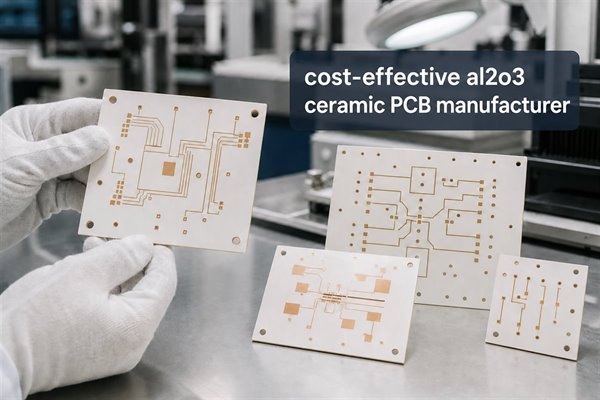
For many electronic products, FR4 PCB is still the most economical PCB material. But when heat, voltage, frequency, size, or reliability requirements become more demanding, alumina ceramic PCB can become a practical and cost-effective option.
The key word is cost-effective, not simply cheap. A low-cost board that fails during assembly or field operation is not economical. A cost-effective Al2O3 ceramic PCB manufacturer should help buyers choose the right ceramic grade, conductor process, copper thickness, tolerance, surface finish, and inspection level for the real application.
Why Choose Al2O3 Instead of Standard FR4?
Al2O3 ceramic PCB is selected when the board material becomes part of the performance requirement. In high-power, high-temperature, high-voltage, compact, or reliability-sensitive designs, the substrate does more than hold copper traces. It affects heat transfer, insulation, mechanical stability, and long-term circuit behavior.
Common reasons to choose Al2O3 ceramic PCB include:
- Better thermal conductivity than standard FR4
- Strong electrical insulation
- Good dimensional stability
- High operating temperature capability
- Good mechanical strength
- Compatibility with thick film, thin film, and DCB ceramic PCB processes
- Reliable performance in harsh or compact environments
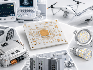
Alumina ceramic PCB is commonly used in LED modules, power electronics, sensors, automotive electronics, industrial control, RF modules, high-voltage circuits, medical electronics, aerospace electronics, and high-reliability assemblies.
Why Al2O3 Is Often More Cost-Effective Than AlN?
Aluminum nitride (AlN) ceramic PCB has higher thermal conductivity than alumina, but it is also usually more expensive. For some power modules and compact thermal designs, AlN is the right choice. However, many products do not need that extra thermal performance.
Al2O3 often gives a better cost-performance balance when the design needs ceramic reliability but does not require the highest possible thermal conductivity.
| Material | Main Advantage | Cost Position | Best Fit |
| Al2O3 ceramic PCB | Stable, reliable, widely used, good insulation, practical thermal performance | More economical ceramic option | LED, sensors, power electronics, RF modules, industrial electronics |
| AlN ceramic PCB | Much higher thermal conductivity | Higher cost | High-power modules, compact heat-critical designs, advanced thermal products |
| FR4 PCB | Lowest cost for many standard circuits | Most economical | General control boards, consumer electronics, low-thermal-stress products |
| Metal core PCB | Good heat spreading with metal base | Often economical for LED and power boards | LED lighting, power conversion, thermal management products |
If a design can meet thermal and electrical requirements with Al2O3, choosing AlN may increase cost without improving the product in a meaningful way. A good ceramic PCB manufacturer should help customers avoid over-specification.
What Makes an Al2O3 Ceramic PCB Cost-Effective?
A cost-effective ceramic PCB is not defined by substrate price alone. The total cost includes material, process complexity, yield, testing, lead time, assembly compatibility, and long-term reliability.
Important cost drivers include:
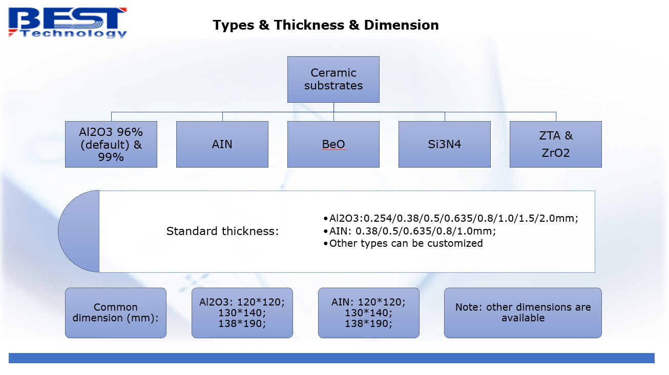
- Ceramic substrate size and thickness
- Alumina purity, such as 96% or 99% Al2O3
- Circuit size and panel utilization
- Conductor material and thickness
- Thick film, thin film, or DCB process selection
- Minimum line width and spacing
- Hole, via, and edge requirements
- Copper thickness or metallization thickness
- Surface finish and solderability requirement
- Tolerance level
- Quantity and delivery schedule
- Electrical test, visual inspection, and reliability test requirements
- Whether PCB assembly or wire bonding is needed
The most cost-effective design is usually the one that matches the process capability without adding unnecessary tolerances. For example, asking for extremely fine lines, tight dimensional control, or special metallization may be necessary in some circuits, but it should be justified by the application.
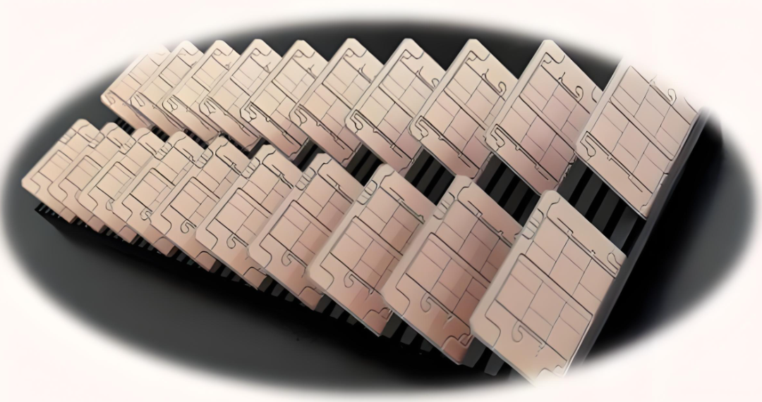
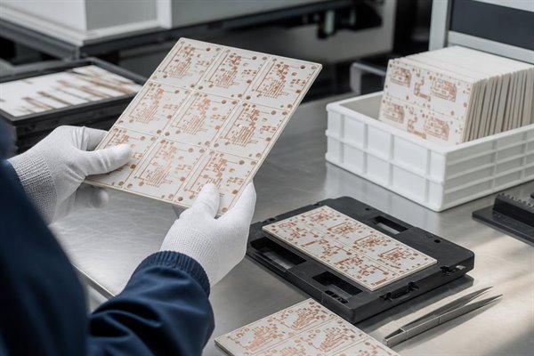
Main Manufacturing Options for Al2O3 Ceramic PCB
Al2O3 ceramic PCB can be manufactured through different processes. The right process depends on circuit density, current load, thermal demand, conductor material, and budget.
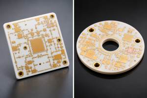
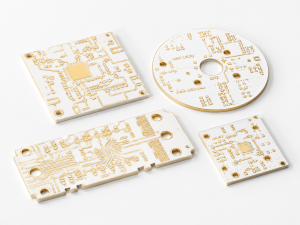
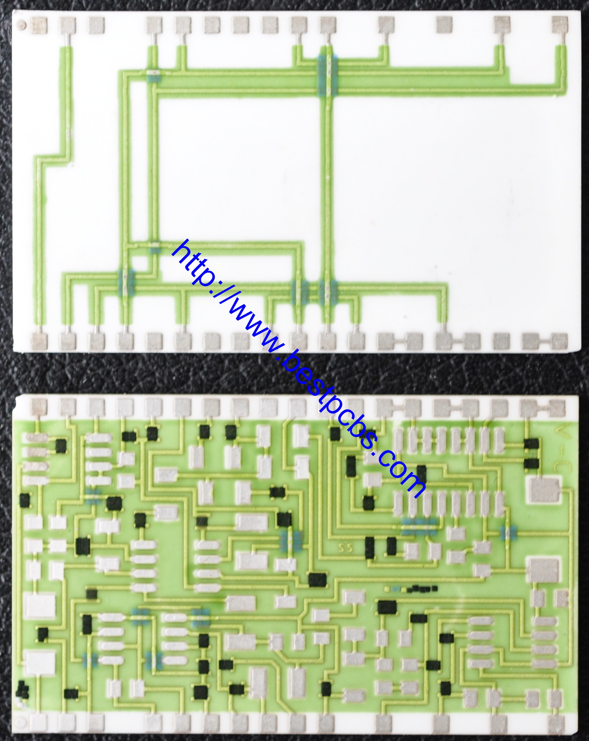
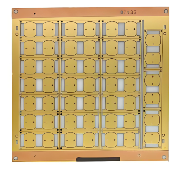
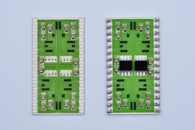
Thick Film Al2O3 Ceramic PCB
Thick film ceramic PCB uses screen printing to apply conductive paste onto the ceramic substrate, followed by high-temperature firing. Silver palladium, gold palladium, or other conductor systems may be used depending on the design.
Thick film is often cost-effective for sensors, hybrid circuits, high-temperature electronics, and moderate-density ceramic circuits. It is useful when the design needs ceramic stability but does not require extremely fine thin-film precision.
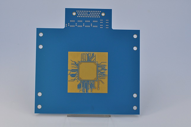
Thin Film Al2O3 Ceramic PCB
Thin film ceramic PCB uses deposited metal layers and photolithography-like processes to create finer and more precise circuit features. It can support tighter line width, spacing, and high-frequency performance compared with many thick film structures.
Thin film Al2O3 ceramic PCB is usually selected when precision is more important than lowest cost. It is common in RF, microwave, sensor, and high-accuracy electronic modules.
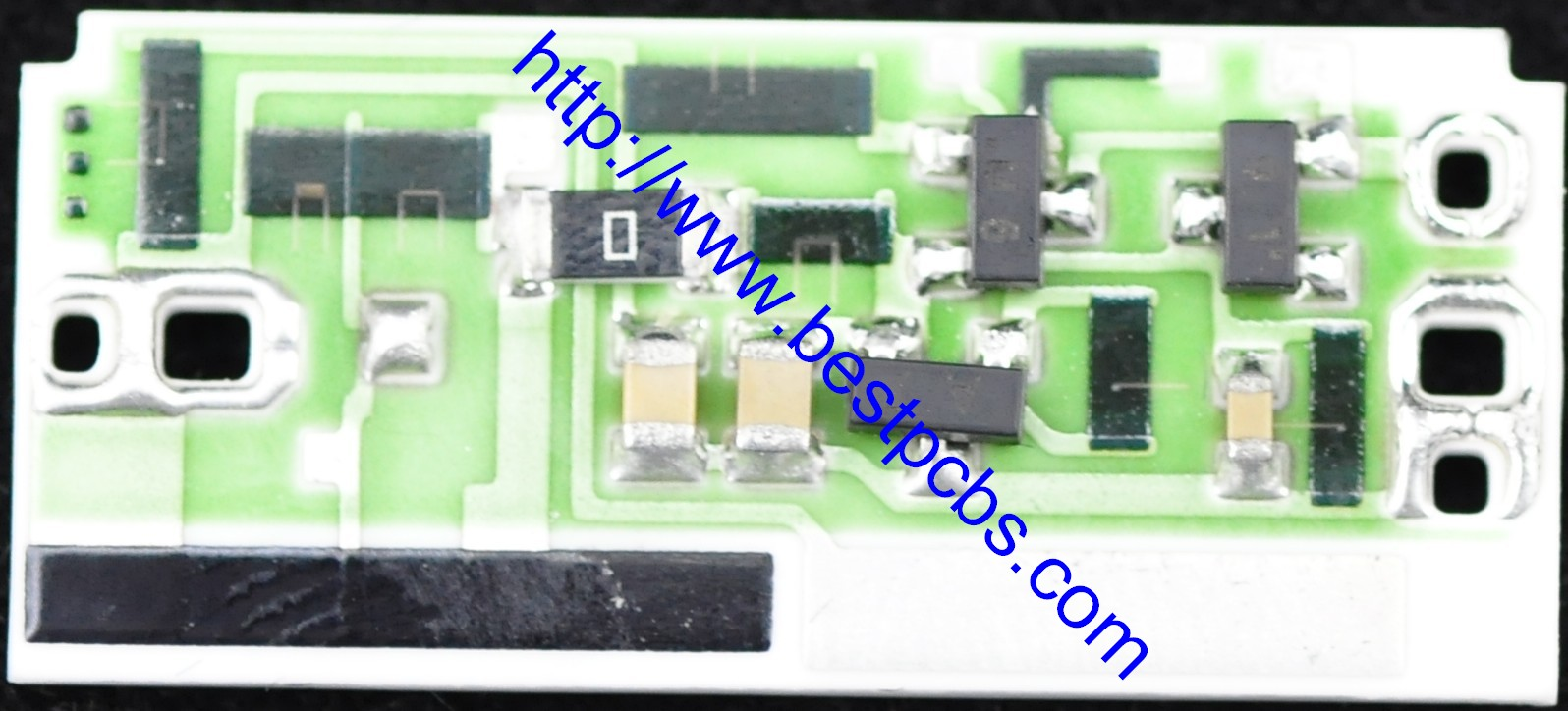
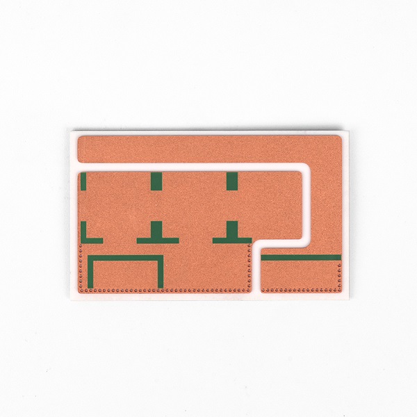
DCB Al2O3 Ceramic PCB
DCB ceramic PCB means direct copper bonded ceramic PCB. In this process, copper is bonded directly to the ceramic substrate under high temperature. DCB ceramic PCB is often used in power electronics because it provides good current capacity, thermal transfer, and reliability.
DCB Al2O3 ceramic PCB can be cost-effective for power modules when the design needs stronger copper and better heat transfer than thick film can provide.
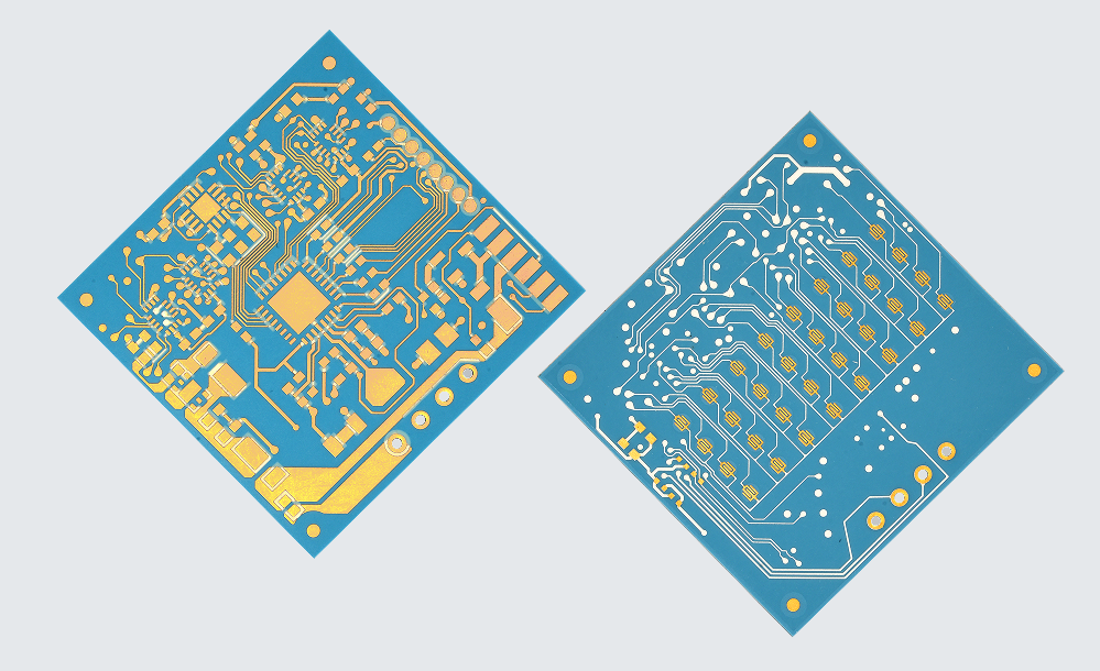
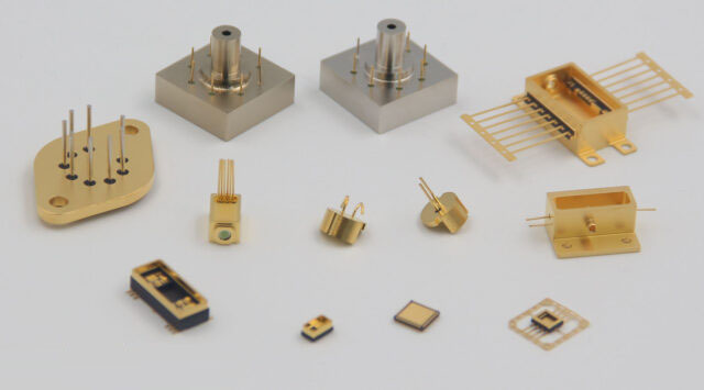
Al2O3 Ceramic PCB Applications
Al2O3 ceramic PCB is used across many industries because it combines ceramic stability with practical manufacturing cost.
Common applications include:
- LED lighting modules
- Power supply modules
- IGBT and MOSFET power circuits
- Automotive electronics
- Industrial control boards
- High-temperature sensors
- Medical electronic modules
- RF and microwave circuits
- Aerospace electronics
- High-voltage insulation circuits
- Laser diode modules
- Battery management and energy equipment
For each application, the board structure should be reviewed against real working conditions. A sensor circuit, LED module, and power module may all use Al2O3, but the conductor process and inspection requirements can be very different.
How to Reduce Cost Without Reducing Reliability?
Buyers can reduce ceramic PCB cost by making the design easier and more stable to manufacture. This does not mean lowering quality. It means removing unnecessary complexity.
Practical cost-saving steps include:
- Choose Al2O3 instead of AlN when thermal requirements allow it
- Use standard substrate thickness when possible
- Avoid overly tight tolerances unless the design needs them
- Keep board outline simple when possible
- Improve panel utilization
- Confirm realistic line width and spacing
- Avoid unnecessary surface finish requirements
- Clarify whether thick film, thin film, or DCB is actually needed
- Separate prototype goals from mass production requirements
- Provide complete files at the quotation stage
- Discuss assembly requirements before finalizing the PCB design
The supplier should review manufacturability before production. A small design change may improve yield and reduce cost without changing circuit performance.
How to Evaluate an Al2O3 Ceramic PCB Manufacturer?
When choosing a cost-effective Al2O3 ceramic PCB manufacturer, buyers should evaluate both price and engineering capability.
Useful supplier checks include:
- Experience with alumina ceramic PCB projects
- Ability to support thick film, thin film, or DCB ceramic PCB
- Clear material options, such as 96% or 99% alumina
- Understanding of thermal, insulation, and tolerance requirements
- DFM review before production
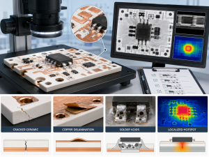
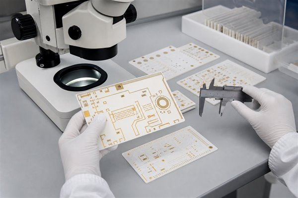
- Stable quality control for metallization, adhesion, surface finish, and dimensional accuracy
- Electrical testing and visual inspection capability
- Prototype and mass production support
- PCB assembly or ceramic PCBA support if needed
- Clear communication about lead time, process limits, and cost trade-offs
The best supplier is not always the one with the lowest first quote. It is the one that can produce the board correctly, explain cost drivers, prevent avoidable defects, and support the project from prototype to production.
What to Send for an Al2O3 Ceramic PCB Quote?
A complete RFQ helps the manufacturer quote faster and more accurately. It also reduces the risk of wrong material, wrong process, or wrong tolerance assumptions.
For a ceramic PCB quote, provide:
- Gerber files
- Drawing or mechanical outline
- Ceramic material, such as Al2O3
- Alumina purity if specified
- Substrate thickness
- Board dimensions
- Copper or conductor thickness
- Thick film, thin film, or DCB process requirement if known
- Minimum line width and spacing
- Hole, slot, or edge metallization requirements
- Surface finish
- Working voltage and current
- Thermal requirement or power dissipation
- Operating temperature range
- Quantity for prototype and mass production
- Inspection or reliability test requirement
- Assembly requirement if PCBA is needed
If you are not sure which process is best, explain the application and performance target. A qualified ceramic PCB manufacturer can help compare thick film, thin film, DCB, Al2O3, AlN, FR4, and metal core PCB options.
When Al2O3 Ceramic PCB May Not Be the Best Choice?
Al2O3 is versatile, but it is not always the right answer.
FR4 may be better when the circuit is low-power, low-temperature, and cost-sensitive. Metal core PCB may be better for some LED and power designs that need heat spreading but do not need ceramic insulation or high-temperature stability. AlN may be better when thermal conductivity is the main limiting factor and the product can justify higher cost.
The goal is not to force every project into alumina ceramic PCB. The goal is to choose the most reliable and economical structure for the real design.
How EBest Circuit Supports Cost-Effective Ceramic PCB Projects?
EBest Circuit (Best Technology) provides custom PCB and PCBA solutions including ceramic PCB, metal core PCB, FR4 PCB, rigid-flex PCB, high frequency PCB, heavy copper PCB, HDI PCB, component sourcing, PCB assembly, and full turnkey service.
For ceramic PCB, EBest Circuit supports alumina ceramic PCB and other ceramic substrate solutions for customers that need thermal stability, insulation, and reliability. The team can review ceramic material, process choice, manufacturability, PCB assembly requirements, and quotation details before production.
This is useful for buyers who want one engineering conversation covering bare ceramic PCB, material selection, process selection, assembly risk, lead time, and cost control.
FAQ
What is an Al2O3 ceramic PCB?
An Al2O3 ceramic PCB is a printed circuit board or circuit substrate made from aluminum oxide ceramic. It is used when the design needs strong insulation, thermal stability, dimensional stability, and reliability in demanding environments.
Is Al2O3 ceramic PCB cost-effective?
Yes, Al2O3 ceramic PCB can be cost-effective when the design needs ceramic performance but does not require the higher thermal conductivity and higher cost of AlN ceramic PCB.
What is the difference between Al2O3 and AlN ceramic PCB?
Al2O3 is usually more economical and widely used. AlN has much higher thermal conductivity but is more expensive. The right choice depends on thermal demand, budget, application, and reliability requirements.
Which is cheaper, Al2O3 ceramic PCB or FR4 PCB?
FR4 is usually cheaper for standard circuits. Al2O3 ceramic PCB is used when FR4 cannot meet thermal, insulation, temperature, or reliability requirements.
What affects the price of Al2O3 ceramic PCB?
Price is affected by material grade, substrate thickness, board size, process type, conductor thickness, line width, spacing, holes, tolerance, quantity, testing, lead time, and assembly requirements.
What is the best process for alumina ceramic PCB?
There is no single best process for every design. Thick film is often practical and cost-effective, thin film is better for fine precision and RF needs, and DCB is suitable for higher-current power applications.
Can Al2O3 ceramic PCB be used for high-temperature electronics?
Yes. Alumina ceramic PCB is commonly used in high-temperature and harsh-environment electronics because of its ceramic stability, insulation properties, and thermal performance.
Can a ceramic PCB manufacturer also provide assembly?
Some manufacturers can provide ceramic PCB assembly or turnkey PCBA support. This is useful when the project needs component sourcing, SMT, wire bonding, testing, or production integration.
Conclusion
A cost-effective Al2O3 ceramic PCB manufacturer should help you balance price, process capability, thermal performance, insulation, reliability, and production yield. Alumina ceramic PCB is often the practical ceramic choice when FR4 is not enough and AlN is more than the application requires.
If you need an Al2O3 ceramic PCB, thick film ceramic PCB, thin film ceramic PCB, DCB ceramic PCB, or ceramic PCBA solution, EBest Circuit (Best Technology) can review your files and help choose a reliable manufacturing path. Contact sales@bestpcbs.com for a quotation and engineering review.