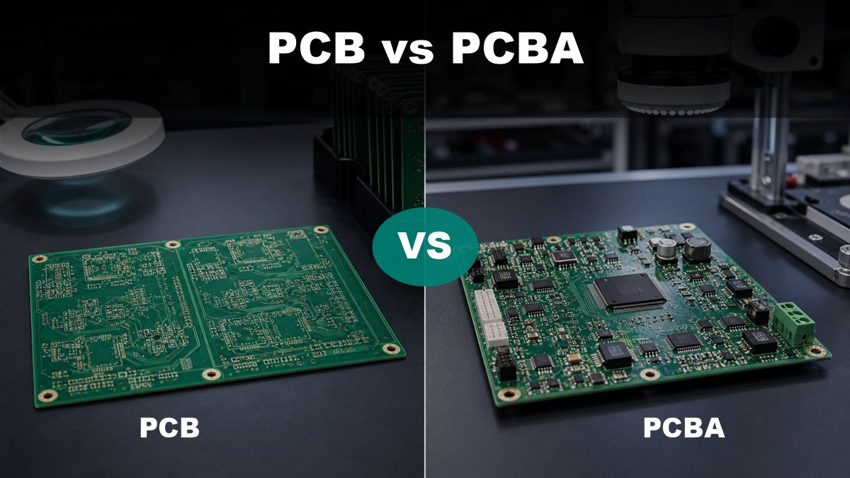
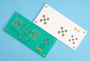
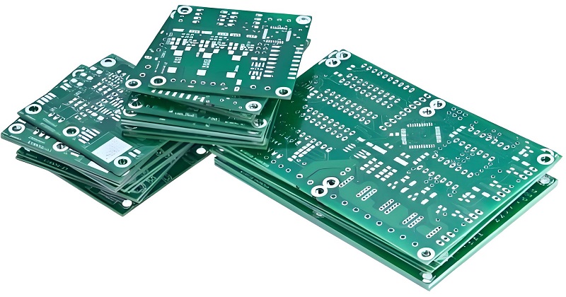
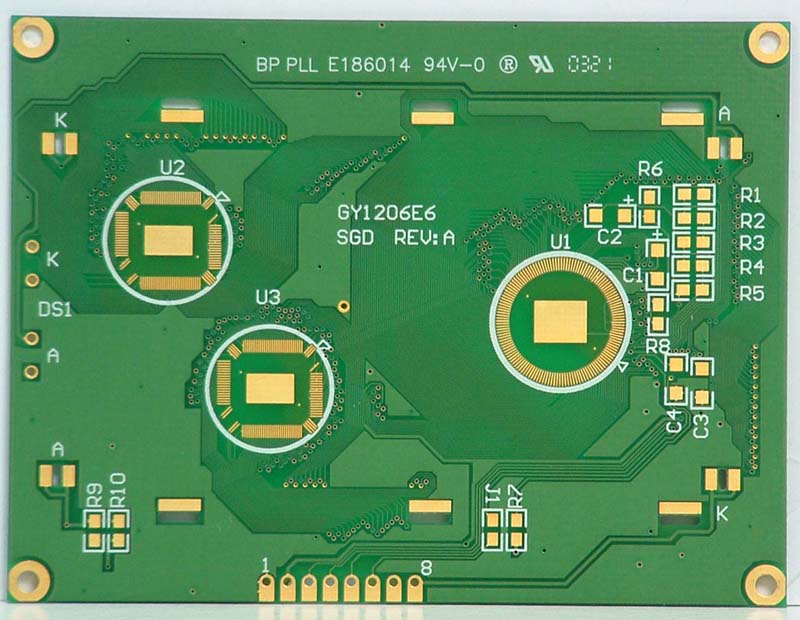
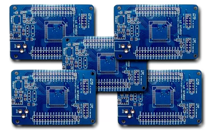
A PCB is the bare printed circuit board: copper traces, solder mask, pads, vias, holes and surface finish, but no assembled electronic components. A PCBA is the completed assembly after components are mounted and soldered onto the PCB, then inspected and tested. In sourcing terms, PCB usually means bare board fabrication, while PCBA means PCB fabrication plus component procurement, SMT or through-hole assembly, inspection and functional checks.
This PCB vs PCBA guide explains the difference from an engineering and purchasing point of view, so you know what to request, what files to prepare and how each choice affects cost, lead time and quality control.
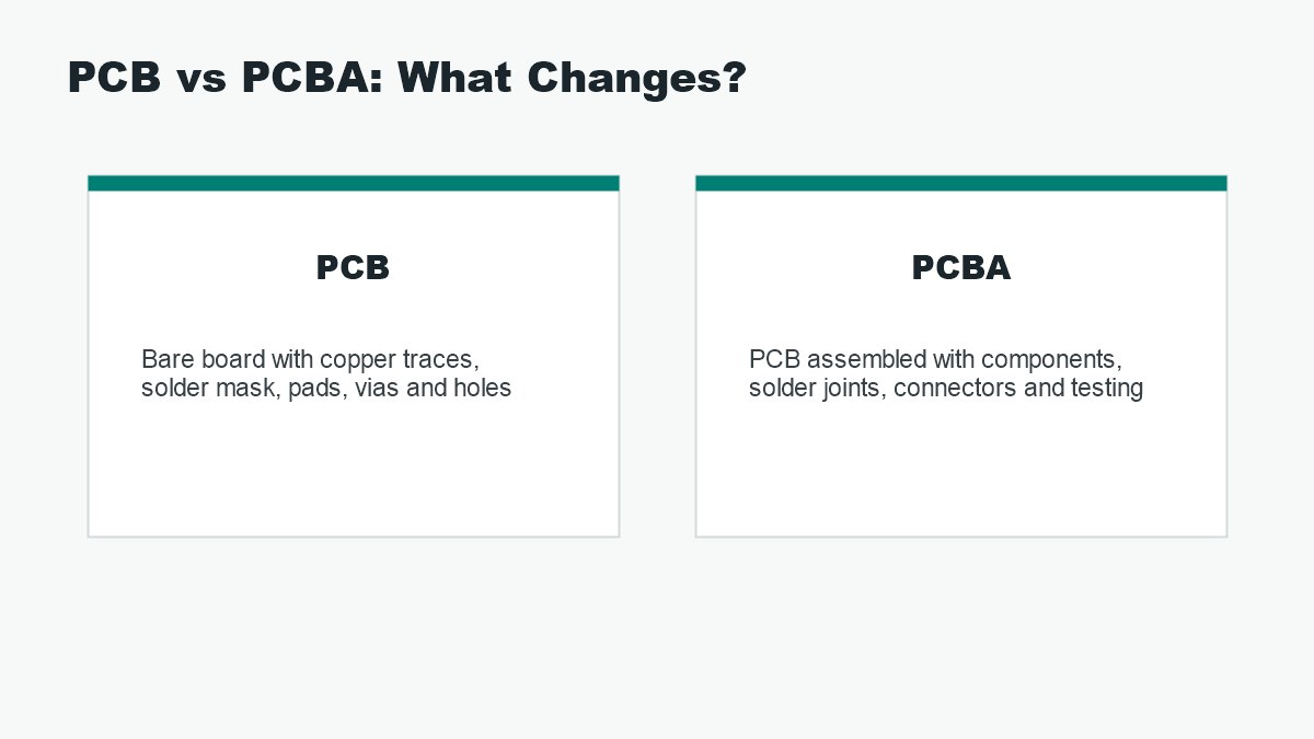
PCB means the bare board; PCBA means the assembled board with components, solder joints and testing.
What Is a PCB?
A PCB, or printed circuit board, is the physical platform that connects electronic components through copper traces. It may include laminate material, copper layers, solder mask, silkscreen, plated holes, vias, pads, slots and a surface finish such as HASL, ENIG or OSP.
A bare PCB does not perform the final product function by itself. It is the circuit carrier. Before components are added, the factory can inspect board dimensions, copper quality, solder mask registration, hole plating, impedance requirements and electrical continuity. For buyers, a PCB order usually requires Gerber files, drill files, stackup notes and fabrication specifications.
What Is a PCBA?
A PCBA, or printed circuit board assembly, is the PCB after electronic components have been installed and soldered. It may include SMT components, through-hole components, connectors, cables, heat sinks, firmware programming and test records depending on the project scope.
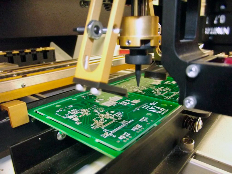
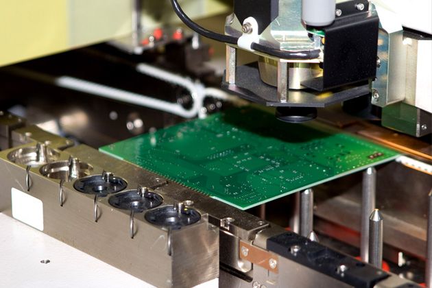
PCBA work is more than placing parts on a board. The supplier must manage component sourcing, stencil setup, solder paste printing, pick-and-place, reflow, through-hole soldering when needed, AOI, X-ray for some packages, cleaning if required, inspection and functional testing. For buyers, a PCBA order usually needs Gerber files, BOM, pick-and-place data, assembly drawings and test requirements.
PCB vs PCBA: The Core Difference
The core difference is assembly status. PCB is the bare board before components; PCBA is the assembled and tested electronic board after components are installed.
The move from PCB to PCBA adds component sourcing, assembly, soldering, inspection and testing.
Item
PCB
PCBA
Meaning
Bare printed circuit board
Printed circuit board assembly
Components
No assembled components
Components mounted and soldered
Main factory work
Board fabrication
Fabrication, sourcing, assembly and test
Files usually needed
Gerber, drill, stackup notes
Gerber, BOM, pick-and-place, assembly notes, test plan
Quality focus
Trace, hole, solder mask, surface finish, electrical test
Solder joints, polarity, component value, function and reliability
Best for
Board-only fabrication or buyer-managed assembly
Turnkey prototypes, samples, validation and production builds
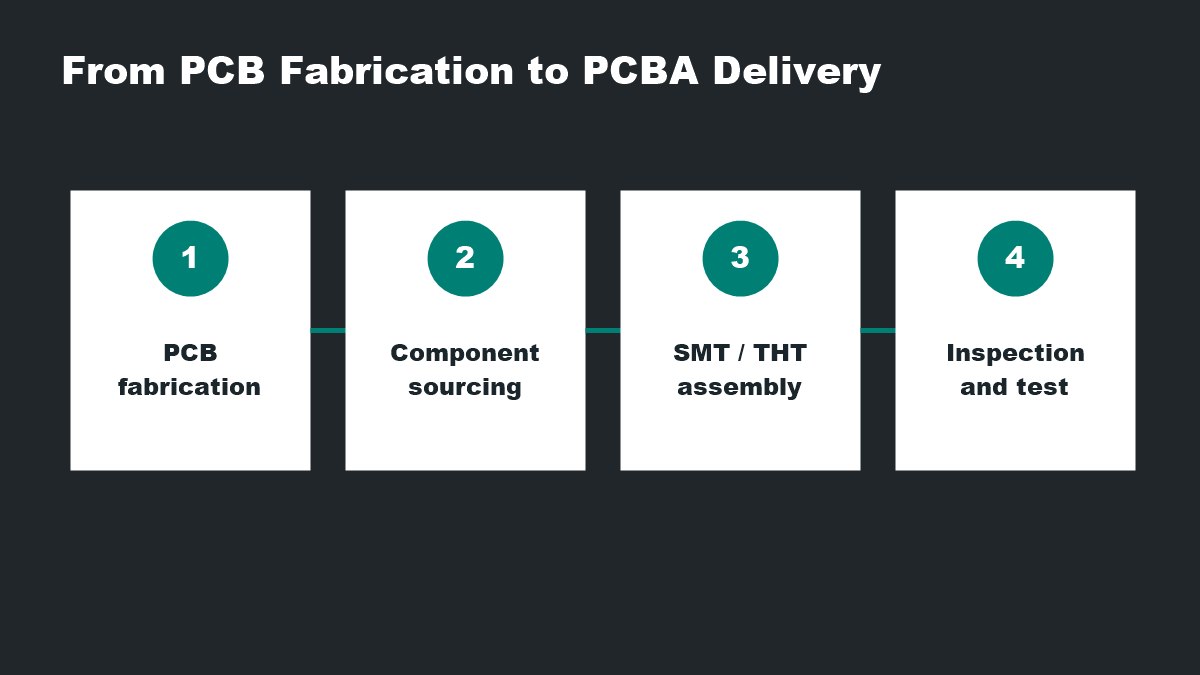
How a PCB Becomes a PCBA
A PCB becomes a PCBA when the bare board moves through component sourcing, solder paste printing, SMT placement, reflow soldering, through-hole assembly when needed, inspection and testing.
PCBA delivery adds assembly and test steps after bare PCB fabrication.
For SMT assembly, solder paste is printed through a stencil, components are placed by machine, and the board goes through reflow. Through-hole components may be soldered by wave soldering, selective soldering or manual soldering depending on volume and design. After that, inspection and testing confirm whether the assembled board meets the order requirements.
Which One Should You Order: PCB or PCBA?
Order a PCB when you only need the bare board or when your team will buy components and assemble the boards elsewhere. Order PCBA when you want one supplier to manage the board, parts, assembly and test process.
PCB-only orders make sense when you already have assembly capability, want to control component purchasing, or need bare boards for internal trials. PCBA is usually better when you need working samples, production builds, functional testing, less handoff risk or one quotation that includes more of the manufacturing work.
The wrong scope can waste time. If you request PCB when you really need PCBA, you may receive good bare boards but still have no working units. If you request PCBA without a clean BOM and assembly data, the supplier may need extra clarification before quoting or building.
Cost Difference Between PCB and PCBA
PCB cost is usually driven by board size, layer count, material, copper thickness, surface finish, hole requirements, impedance control, panelization and quantity. PCBA cost adds component cost, sourcing risk, stencil, placement, soldering, inspection, test fixture needs and labor.
For simple boards, the bare PCB may be a small part of the total assembled product cost. For complex assemblies, component availability and testing can matter more than board fabrication price. Buyers should compare quotes by scope, not by headline price. A PCB quote and a PCBA quote are not equivalent unless the included work is the same.
Quality Control: PCB vs PCBA
PCB quality control checks whether the bare board was fabricated correctly. PCBA quality control checks whether the full assembled circuit was built correctly and can work as intended.
For PCB fabrication, common checks include electrical test, visual inspection, hole plating review, solder mask inspection and dimensional checks. For PCBA, the inspection scope may include solder paste quality, component placement, polarity, solder joint quality, AOI, X-ray for hidden joints, ICT or functional testing. The more complete the assembly, the more important test planning becomes.
Files Needed for PCB and PCBA Quotes
PCB and PCBA quotes need different document packages. Sending the right files early helps avoid delays and wrong assumptions.
For PCB: Gerber files, drill files, board thickness, copper weight, layer count, material, surface finish, solder mask color and special requirements.
For PCBA: PCB files plus BOM, pick-and-place file, assembly drawing, component polarity notes, programming requirements, test plan and packaging requirements.
For turnkey PCBA: approved alternates, manufacturer part numbers, substitute rules and critical component notes are especially useful.
Common Buyer Mistakes
Many PCB vs PCBA problems happen because the order scope is unclear. A buyer may ask for a PCB quote while expecting assembled boards, or send a BOM without confirming footprints and polarity.
Before requesting a quote, decide whether you need bare boards, consigned assembly, turnkey PCBA, prototype assembly or mass production. Check that every component in the BOM has a package, value, manufacturer part number when needed and a matching footprint. If the board needs firmware, test points or a fixture, mention that before production starts.
FAQ
Is PCB the same as PCBA?
No. PCB means the bare printed circuit board. PCBA means the printed circuit board assembly after components are mounted, soldered, inspected and tested.
What does PCBA stand for?
PCBA stands for printed circuit board assembly. It refers to a PCB that has been assembled with electronic components and is ready for inspection, testing or product integration.
Can I order PCB fabrication without assembly?
Yes. If you only need bare boards, order PCB fabrication. You will still need a separate assembly plan if the boards must become working electronics.
What files are needed for PCBA?
PCBA usually needs Gerber files, drill files, BOM, pick-and-place data, assembly drawings, polarity notes and test requirements. Turnkey assembly also needs clear component sourcing rules.
Why is PCBA more expensive than PCB?
PCBA includes more work: component sourcing, stencil, SMT or through-hole assembly, soldering, inspection, testing and handling. The components themselves can also cost more than the bare board.
Which is better for prototypes, PCB or PCBA?
If you only want to check board fabrication, PCB is enough. If you need working samples for validation, firmware, testing or customer review, PCBA is usually the right scope.
Does PCBA include functional testing?
Not always. Functional testing must be defined in the order scope. Some PCBA orders include only assembly and visual inspection, while others include ICT, programming or custom functional tests.
Can the same supplier handle PCB and PCBA?
Yes, many suppliers can support both PCB fabrication and PCBA. This can reduce handoff issues, but the buyer still needs to provide complete files, approved components and clear test requirements.
Final Thoughts
The simplest way to remember PCB vs PCBA is this: PCB is the board, PCBA is the assembled electronic board. If you need only fabricated boards, request PCB. If you need working assemblies, request PCBA with BOM, placement data and test requirements.
If you are sourcing PCB fabrication or turnkey PCBA for prototypes, sample builds or production, BestPCBs can help review fabrication details, assembly requirements and quotation scope. Contact the engineering team at sales@bestpcbs.com for technical support and a quote.
Chinese PCB manufacturers dominate the global market with their competitive pricing, advanced technology, and fast production capabilities. As one of leading Chinese PCB maker, EBest Circuit (Best Technology) offers a wide range of PCB solutions whether you’re looking for small-batch prototypes or large-scale production. There are numerous cheap Chinese PCB manufacturer available, choosing the right one requires careful evaluation. This article provide you with printed circuit board manufacturers list, to help you find the reliable Chinese PCB manufacturers to suit your project.
Located in Shenzhen, EBest Circuit (Best Technology) provides manufacturing and sale service of various types of printed circuit boards and assembly. During the 18 years, EBest Circuit (Best Technology) focused on oversea market and implemented the professional separation of sales and production. So that we can provide more efficient service to customer and going to be one of the most reliable PCB manufacturers in China. Warmly welcome to contact us at sales@bestpcbs.com for any custom PCB projects of any quantity, from small to large volumes.
Top Chinese PCB Manufacturers
China is home to some of the world’s leading PCB manufacturers. These companies provide various options, from prototypes to high-volume production. Here are the top 10 PCB manufacturers in China:
1. EBest Circuit (Best Technology) Co., Limited: A leader in high-quality PCBs manufacturing includes multilayer FR4 PCB, ceramic PCB, metal core PCBs, PCB assembly. Offers rapid PCB prototyping and assembly services.
2. Shenzhen Kinwong Electronic Co., Ltd.: A top supplier known for advanced PCB solutions and reliability.
3. Suntak PCB: Offers high-precision circuit boards for industrial and consumer electronics.
4. Victory Giant Technology: Well-known for producing high-end PCBs for global customers.
5. Aoshikang Technology: Focuses on high-frequency and high-speed PCBs.
6. Shennan Circuits: Supplies PCBs to aerospace, medical, and telecommunications industries.
7. Jiangxi Copper (JCC): A company in PCB copper materials and circuit board production.
8. Wuzhu Technology: Specializes in quick-turn and HDI PCB solutions.
9. Sihui Fuji Electronics Technology: Provides a balance of cost and performance in PCB manufacturing.
10. Shenzhen Fastprint: Offers PCB, IC substrate, FPC, semiconductor test board products.
How Do I Find the Best Manufacturer in China?
Finding the best manufacturer in China requires a mix of research, due diligence, and relationship-building. Below is a step-by-step guide to streamline your search while ensuring quality and reliability:
1. Define Your Product Requirements
Specifications: Materials, dimensions, certifications (e.g., ISO, CE), and compliance standards.
Volume: Estimate order quantities to target manufacturers that align with your scale.
Budget: Balance cost with quality—avoid prioritizing low prices alone.
This clarity helps filter manufacturers that meet your needs and reduces miscommunication later.
2. Leverage Trusted Sourcing Platforms
Use established B2B platforms to shortlist candidates:
Alibaba.com: Filter verified suppliers with “Gold Supplier” or “Trade Assurance” badges.
Global Sources: Focus on exporters with audited profiles.
Made-in-China: Ideal for niche industries or custom products.
Exhibition: Attend trade shows like the Canton Fair to meet PCB suppliers face-to-face. Keep regular communication which fosters trust.
It is recommended to Look for suppliers with ≥3 years of operation and consistent reviews.
3. Verify Credibility
Requesting Business Licenses: Legitimate manufacturers will provide a Chinese business license.
Checking Export Experience: Ask for past client references in your region.
Third-Party Inspections: Hire agencies like SGS or Bureau Veritas to audit facilities or test samples.
Visit Factories: If feasible, tour facilities to assess equipment, workflows, and working conditions. For remote vetting, schedule a video walkthrough.
4. Request Samples
Request Samples: Test functionality, durability, and packaging.
5. Mitigate Supply Chain Risks
Draft Clear Contracts: Include IP protection, penalties for delays, and quality clauses.
Start Small: Place a trial order before committing to large volumes.
Use Secure Payments: Opt for escrow services (e.g., Alibaba Trade Assurance) or letters of credit (L/C).
By combining thorough research with proactive verification, you’ll minimize risks and partner with a manufacturer that delivers consistent quality and aligns with your business goals.
Who Makes Fast Turnaround PCBs?
For urgent projects, selecting a China PCB manufacturer that specializes in fast delivery is essential. EBest Circuit (Best Technology) is known for quick turn services.
We always do right things and then do things right, so that we can complete any project quickly & efficiently. We always reply email within 12 hours so that make our customers feeling like doing business with the neighbor. Focusing on electronics & circuit board industry, EBest Circuit (Best Technology) provide one-stop service from designing, DFM, fabrication of all type of printed circuit boards (from MCPCB, ceramic PCB, FR4 PCB, special PCB), to components purchasing, PCBA (SMT) and box assembly, we also provide suitable solution for our customers that help to save time & money of them, and then become the most reliable Chinese PCB manufacturer r of them.
If you need PCB prototype, pls feel free to reach out to EBest Circuit (Best Technology) at sales@bestpcbs.com at any time. EBest Circuit (Best Technology) provides rapid prototypes within 24-48 hours. We have offered more than 1,200 customers in more than 60 countries & areas the fast turnaround PCBs service. We provide both normal delivery service and fast service, and urgent boards can be shipped out within 24 hours!
What Is EBest Circuit (Best Technology) Co., Limited China?
Founded in 2006, EBest Circuit (Best Technology) is one of a direct Chinese PCB manufacturers with in-house production capabilities, own certificate like ISO 9001, ISO 13485, IATF 16949, AS9100D. We specialize in various PCBs, including:
Metal Core PCBs: Includes single-layer metal core PCB, two-layer aluminum base PCB, multilayer aluminum based PCB, double-sided metal core PCB.
These are ideal for LED applications (e.g., automotive headlights, outdoor displays) due to excellent heat dissipation.
These are High thermal conductivity for RF communications (5G base stations, radar systems) and power electronics (IGBT modules, new energy vehicle control systems), and aerospace applications.
Printed Circuit Boards: Includes single sided PCB, multi-layer PCB, semi rigid flex PCB, RF PCB.
These are suitable for consumer electronics (smart home devices, wearables), industrial controls (PLCs, sensors), and communication equipment (routers, switches), balancing cost-effectiveness and performance optimization.
Special PCBs: Providing custom PCBs like busbar PCB, IC substrate, HDI PCB, extra thin PCB, heavy copper PCB, high Tg PCB, high speed PCB, impedance control PCB.
These meet stringent reliability requirements in automotive electronics (ADAS systems, battery management), medical devices (imaging diagnostics, portable monitors), and military equipment (precision guidance, anti-interference systems).
All our above PCB products can be customized to suit your needs, all our PCBs are compliant to REACH, RoHS. Let you no worries about the quality. Currently our mouthy capability is 260,000 square feet (28,900 square meter), more than 1,000 different boards will be completed. EBest Circuit (Best Technology) focus on quality, innovation, and customer satisfaction. We provide fast turnaround service, so that urgent boards can be shipped out within 24 hours.
How to Compare Prices: Chinese vs. Non-Chinese PCB Manufacturers?
Comparing pricing between Chinese PCB manufacturers and global competitors helps in making informed decisions. Here’s what to consider:
1. Material Costs: China often has lower raw material costs, reducing overall expenses.
2. Labor Costs: Manufacturing in China is more cost-effective than in Europe or North America.
3. Technology & Equipment: Leading Chinese PCB makers use advanced technology while maintaining competitive prices.
4. Shipping & Tariffs: Factor in logistics and import duties when comparing global prices.
5. Lead Time: Chinese suppliers often have faster production due to efficient supply chains.
In general, China PCB manufacturers offer better pricing without compromising on quality.
What Are the Benefits of Choosing a Chinese PCB Manufacturer?
Selecting a Chinese PCB manufacturer provides several advantages:
Cost-Effective Production: Lower manufacturing costs lead to competitive pricing.
Advanced Technology: Many factories use cutting-edge equipment for high precision.
Scalability: Handles small to mass production with flexibility.
Fast Prototyping: Quick turnaround times for new product development.
Global Supply Chain: Strong logistics networks ensure smooth international shipping.
Customization: Tailored PCB solutions for various industries.
Chinese PCB manufacturers continue to be a preferred choice for companies worldwide.
How to Choose a PCB Manufacturer?
When selecting a Chinese PCB manufacturer, keep these points in mind:
1. Industry Experience: Look for companies with a strong track record.
2. Quality Standards: Ensure compliance with international certifications.
3. Customization Ability: The manufacturer should meet specific design needs.
4. Customer Service: A responsive team can resolve issues quickly.
5. Production Capacity: Choose a supplier that can scale with your business.
6. Pricing & Lead Time: Find a balance between cost and delivery speed.
In conclusion, Chinese PCB manufacturers offer a mix of affordability, quality, and advanced technology. Whether you need good price and quality mix lamination PCB from Chinese manufacturers or a fast-turnaround prototype, there are plenty of options. Research thoroughly, compare suppliers, and choose a manufacturer that aligns with your requirements.
By partnering with the right Chinese PCB manufacturers, you can ensure cost-effective, high-quality solutions for your electronic projects. If you’re looking for reliable PCB production, EBest Circuit (Best Technology) Co., Limited is a strong choice with proven expertise in the industry. Just feel free to contact us at sales@bestpcbs.com for any PCB specification or PCB quotations.
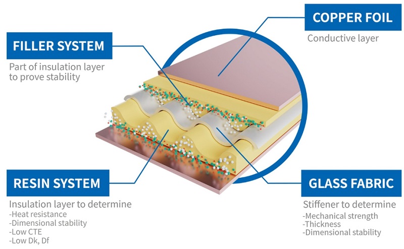
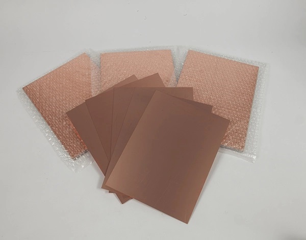
Copper clad laminate (CCL) is crucial in printed circuit boards (PCBs), providing structural integrity and conductivity. Whether you are a PCB designer, engineer, or manufacturer, understanding CCLs will help you choose the right materials for your applications. In this guide, we explore CCL types, uses, and pricing, along with an in-depth look at its manufacturing process.
EBest Circuit (Best Technology) offers comprehensive PCB manufacturing solutions, seamlessly integrating design, prototyping, assembly, component sourcing, and 360° technical support across the entire project lifecycle. Leveraging advanced lamination systems and high-precision CNC drilling machines from Hitachi and Timax, we ensure exceptional accuracy in multilayer PCB fabrication. Backed by a seasoned R&D team and engineers with over 10 years of industry experience, we guarantee a prompt response within 12 hours. Punctual delivery is our commitment, ensuring your projects stay on track. Feel free to reach out to us at sales@bestpcbs.com for any copper-clad laminate PCB needs.
What is Copper Clad Laminate?
Copper clad laminate (CCL) is a composite material made of a non-conductive substrate (such as fiberglass, resin-impregnated paper), filler, and other chemicals, with a thin copper foil layer bonded to one or both sides. It serves as the foundation for PCB fabrication, ensuring electrical pathways are properly formed while offering mechanical support. CCLs are widely used in consumer electronics, automotive applications, and industrial equipment.
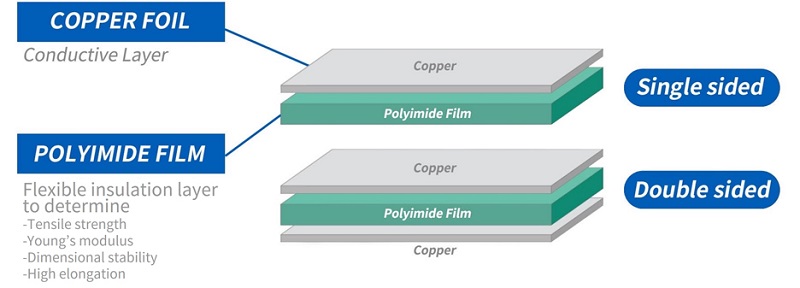
What is Flexible Copper Clad Laminate?
Flexible copper clad laminate (FCCL) is a variation of CCL that uses a flexible substrate instead of rigid fiberglass. The most common substrate materials include polyimide or polyester, and FCCL is produced by laminating copper foil onto polyimide film (PI), making FCCLs suitable for bendable and lightweight applications. These laminates are commonly found in wearables, foldable devices, and medical electronics, where flexibility is a key requirement.
What is Copper Clad in PCB?
In PCB manufacturing, copper clad laminate acts as the base material that undergoes etching, drilling, and layering processes to create functional circuits. The copper layer allows for efficient electrical conductivity, while the substrate provides insulation and mechanical support. PCBs can have single-sided, double-sided, or multi-layer configurations, depending on design complexity.
What are the Different Types of Copper Clad Laminate?
There are several types of CCLs, each designed for specific performance requirements:
FR-4 – The most widely used CCL, composed of woven glass fabric and epoxy resin, offering excellent electrical insulation and thermal resistance.
CEM-1 – A cost-effective option with a paper-based core and fiberglass reinforcement, ideal for single-sided PCBs.
CEM-3 – Similar to FR-4 but with a finer glass weave, providing better flexibility and processing ease.
Flexible Copper Clad Laminate (FCCL) – Uses polyimide or polyester as a base, enabling use in applications requiring bending or flexing.
Metal Core CCL – Features an aluminum or copper core for better heat dissipation, commonly used in LED lighting and power electronics.
High-Frequency CCL – Designed for RF and microwave applications, using PTFE or ceramic-based substrates for improved signal integrity.
What is the Difference Between Copper and Copper Clad?
Copper is a pure metal known for its excellent electrical and thermal conductivity. Copper clad laminate, however, is a composite material where a thin copper layer is bonded to an insulating substrate. While pure copper is used in electrical wiring and heat exchangers, copper clad laminates serve as the base for PCBs, allowing for structured circuit pathways while maintaining mechanical stability.
What is the HS Code for Copper Clad Laminates?
The Harmonized System (HS) code 7410.11 is widely used for copper clad laminates in international trade. This classification applies to materials consisting of copper foil (printed or unprinted) bonded to an insulating substrate such as fiberglass, epoxy resin, paper, or other dielectric layers.
7410.11: Covers copper foil laminated with insulating materials, regardless of surface patterning. These laminates serve as core materials for manufacturing printed circuit boards (PCBs), enabling electrical conductivity and structural support.
Critical Considerations:
Regional Variations: Some jurisdictions classify PCB-ready laminates (pre-etched or pre-engineered for circuitry) under 8547.20 (“printed circuits”).
Example: China may categorize advanced laminates under 8547.20 if they are explicitly designed for PCB production.
Material-Specific Codes: Laminates with plastic-based substrates (e.g., phenolic resin) might fall under 3921.90 (“plastic laminates”).
Verification: Pls consult local customs or a licensed broker for binding rulings in necessary situation, as interpretations vary. For instance:
U.S. HTS: May use 7410.11.0000 for basic laminates.
EU TARIC: Could require additional subcodes based on thickness or resin type.
What is the Price of Copper Clad?
Copper clad laminate price varies based on copper thickness, substrate type, material grade, order volume, and market demand. For PCB buyers, this material cost is only one part of the final PCB quotation, but it can strongly affect FR4 PCB, high-frequency PCB, heavy copper PCB, and other custom board projects. Here are the key factors that impact pricing:
Copper Thickness – Thicker copper layers increase cost due to the higher material requirement.
Substrate Material – FR-4 is pricier than paper-based laminates like CEM-1.
Processing Complexity – Advanced CCLs with high-frequency capabilities cost more to manufacture.
Market Demand – Prices fluctuate based on raw material availability and global market trends.
Order Volume – Bulk purchases typically come with lower unit costs.
Standard FR-4 CCLs typically range from $5 to $15 per square meter, while high-performance laminates designed for RF applications can cost significantly more.
What is the Manufacturing Process of Copper Clad Laminate?
What is copper clad laminate manufacturing process? Manufacturing copper clad laminate involves precise processes to ensure consistent quality and performance. Here take the double-sided copper clad laminate as a case. The production of double-sided copper clad laminates generally follows these steps:
1. Film Printing – Prepare and print the design film.
2. Board Cutting – Cut the board to size, keeping a 20mm process edge.
3. Drilling – Set the board thickness to 2.0mm or 1.6mm, ensuring the drill tip is 1-1.5mm above the PCB surface. Use Create-DCM software to generate U00 format drill files for CNC machines.
4. Polishing – Remove surface oxidation, oil stains, and burrs from drilling.
5.Hole Inspection – Ensure hole clarity for proper chemical penetration. Inspect the drilled and polished board under light to check if the holes are clear and unobstructed.
6. Pre-soaking – Remove oil, oxidation, and copper powder while adjusting the charge for better carbon particle adsorption.
7. Water Rinsing – Thoroughly rinse with clean water to remove chemical residues.
8. Drying – Eliminate residual moisture inside the holes using a drying oven or electric blower.
9. Activation – Coat the inner hole walls with nano-carbon particles to enhance conductivity.
10.Through-Hole Processing – Remove excess activation liquid to ensure all holes remain open using a vacuum cleaner.
11.Curing – Secure carbon particles to the hole walls and dry them with airflow.
12. Repeat Steps 9-11 for better adhesion.
13.Micro-etching – Remove excess carbon particles and wipe off black residues from the copper surface.
14. Water Rinsing – Clean the board thoroughly.
15. Copper Plating – Immerse in a copper plating bath for 20-30 minutes at a current of approximately 3-4A/d㎡ (adjust as needed). This process ensures electrical conductivity by plating copper on the hole walls.
16. Water Rinsing – Clean the surface after plating.
17.Drying – Dry the board and remove any residual moisture in the holes.
18.Lamination – Apply the dry film using a lamination machine.
19. Exposure – Expose the film to light for approximately 3 minutes. Align the film (negative film at this stage) with the board first. Ensure correct alignment of the negative film for double-sided circuits.
20.Developing – Remove unexposed film in a developing solution at 45-50°C while observing changes on the board.
21. Water Rinsing – Rinse thoroughly to remove residues.
22. Etching – Etch at 45-50°C to remove unwanted copper.
23. Water Rinsing – Wash off any remaining etchant to prevent further corrosion.
24. Stripping – Use a strong alkaline solution to remove the dry film.
25. Water Rinsing – Rinse thoroughly.
26. Drying – Dry the board completely.
27.Tin Plating – Perform micro-etching, rinsing, and tin plating to protect exposed copper areas from oxidation and improve solderability.
28. Edge Cutting – Trim off excess material from the fabricated board based on the circuit outline and smooth the board edges using a manual grinding tool.
This process ensures high-quality double-sided copper clad laminate for various PCB applications.
Copper Clad Laminate Manufacturers
Several manufacturers produce high-quality copper clad laminates for different industries. Some of the leading names include:
Doosan Corporation Electro-Materials – A global leader in FR-4 and high-performance CCL production.
Shengyi Technology – Specializes in advanced CCLs for high-frequency and RF applications.
Rogers Corporation – Renowned for high-frequency laminates used in 5G and aerospace applications.
DuPont – Known for high-reliability materials like polyimide-based CCLs for flexible circuits and high-temperature applications.
EBest Circuit (Best Technology) Primarily dedicated to PCB manufacturing, we also source and supply copper clad laminates, providing customers with reliable materials tailored to their specific requirements.
In conclusion, copper clad laminate plays a vital role in PCB manufacturing, influencing performance, cost, and durability. Understanding its manufacturing process, types, and pricing helps engineers and buyers make better decisions. Whether you need rigid FR-4 laminates or flexible options for advanced applications, choosing the right material ensures optimal performance and reliability.
For those sourcing copper clad laminates, partnering with a reputable manufacturer guarantees high-quality materials and consistent supply. We provide one-stop PCB manufacture service, including PCB assembly and component purchasing and all-around technical support before and after-sales. Just feel free to reach out to us at sales@bestpcbs.com for any printed circuit board needs.
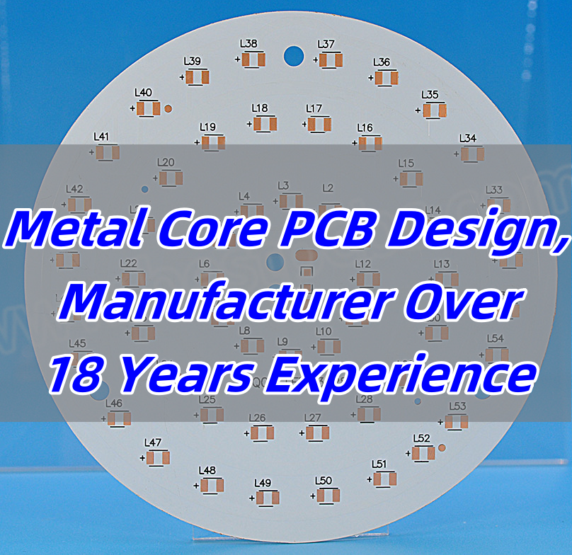
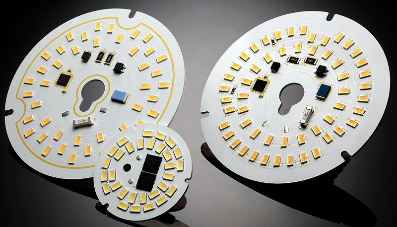
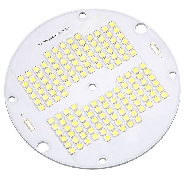
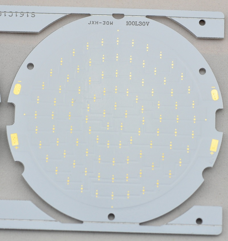
Metal core PCB is designed for applications requiring efficient heat dissipation, making it ideal for high-power electronics. Unlike standard PCBs, it features a metal base, typically aluminum or copper, that enhances thermal conductivity and improves durability. This design helps prevent overheating, ensuring stable performance in LED lighting, automotive systems, and power electronics. As industries demand reliable and heat-resistant circuit boards, metal core PCBs have become a preferred choice.
EBest Circuit (Best Technology) has over 18 years of experience designing metal core PCBs. We are a professional metal core PCB manufacturer, mainly involved in all types of PCB manufacturing. If you need a metal core PCB, please feel free to contact us at sales@bestpcbs.com.
What is a Metal Core PCB?
A metal core PCB (MCPCB) is a specialized type of printed circuit board that features a metal core instead of the standard FR4 or other non-metallic substrates. The metal core, typically made of aluminum, copper, or steel, helps dissipate heat efficiently, making it a preferred choice for high-power applications such as LED lighting, automotive electronics, and power conversion systems.
Unlike regular PCBs, which rely on thermal vias or external heat sinks for cooling, MCPCBs conduct heat directly through their metal base. This results in better thermal management, increased reliability, and a longer lifespan for electronic components. If you’ve ever wondered why some circuit boards perform better under high temperatures, chances are they are using metal core PCB technology.
What Are the Different Types of Metal Core PCBs?
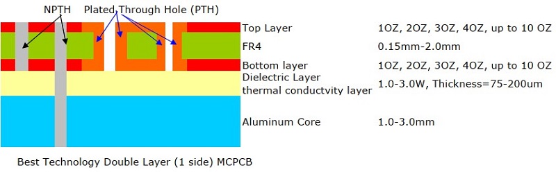
Metal Core PCBs (MCPCBs) are classified based on three key dimensions: Layer Structure, Heat Dissipation, Application-Specific Features.
1. Classification by Layer Structure
Single-Layer MCPCB
Structure: A metal base, an insulating dielectric layer, and a single copper layer for circuit traces.
Best For: LED lighting, power supplies, and basic thermal management applications.
Key Benefit: Simple and cost-effective with efficient heat dissipation.
Two-Layer MCPCB
Structure: Two copper layers put on the one side of MCPCB, with an aluminum or copper base.
Best For: Power circuits requiring more routing flexibility than single-layer MCPCBs.
Key Benefit: Improved circuit complexity and higher current capacity.
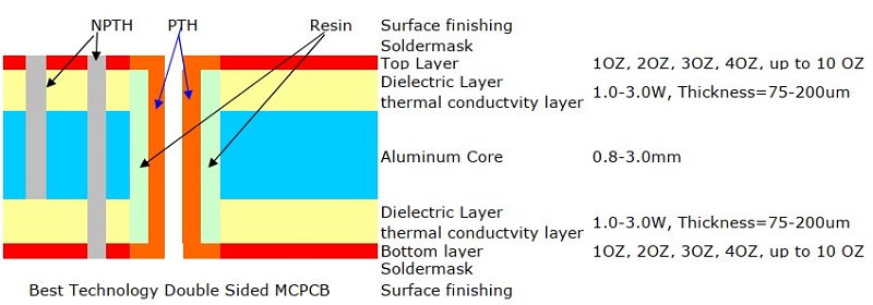
Double-Sided MCPCB
Structure: Copper layers on both sides of the metal core, connected via plated through-holes (PTHs).
Best For: Automotive control systems, industrial power converters, and motor drivers.
Key Benefit: Enhanced circuit routing options and improved electrical performance.
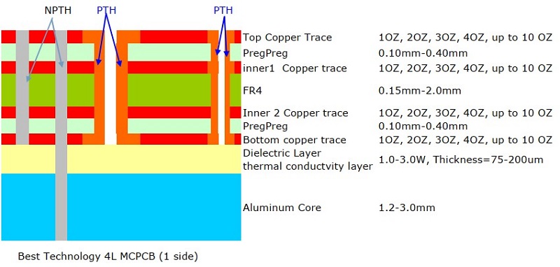
Multilayer MCPCB
Structure: Multiple copper and dielectric layers stacked on a metal core.
Best For: Advanced applications like aerospace, telecommunications, and high-power LED lighting.
Key Benefit: Increased circuit density, better signal integrity, and superior heat dissipation.
2. Classification by Heat Dissipation Technology
Standard MCPCB
Structure: A conventional metal core PCB with a dielectric layer that transfers heat from components to the metal base.
Key Benefit: Moderate thermal performance, widely used in consumer electronics and LED modules.
SinkPAD MCPCB (Enhanced Thermal Management)
SinkPAD is a specialized MCPCB technology designed for superior heat dissipation by reducing thermal resistance. Unlike standard MCPCBs, SinkPAD boards allow heat to transfer directly from the component to the metal base without passing through an insulating dielectric layer.
1L SinkPAD Board (Single-Layer SinkPAD)
Structure: A single copper layer with direct thermal pathways to the metal core.
Best For: High-power LED modules and power supplies requiring fast heat dissipation.
Key Benefit: More efficient cooling than standard single-layer MCPCBs.
2L SinkPAD Board (Two-Layer SinkPAD)
Structure: Two copper layers with a thermal connection to the metal core.
Best For: Medium-power applications, such as LED drivers and automotive lighting.
Key Benefit: Improved thermal performance and better electrical conductivity.
Double-Sided SinkPAD Board
Structure: Copper layers on both sides of the metal core, providing heat dissipation pathways on both surfaces.
Best For: High-power industrial electronics, automotive systems, and power management circuits.
Key Benefit: Balanced thermal performance and high electrical efficiency.
Multi-Layer SinkPAD Board
Structure: Multiple copper layers with direct heat dissipation channels integrated into the metal core.
Best For: Aerospace, military, and high-end LED applications requiring extreme heat management.
Key Benefit: Maximized thermal efficiency for complex, high-power circuits.
3. Classification by Application-Specific Features
COB (Chip-on-Board) MCPCB
Structure: LED chips are mounted directly onto the metal core PCB without individual packaging.
Best For: High-brightness LED applications such as streetlights, automotive headlights, and stadium lighting.
Key Benefit: Lower thermal resistance, higher efficiency, and reduced size compared to traditional LED modules.
Selecting the right MCPCB depends on your thermal management needs, power requirements, and circuit complexity. For simple applications, a single-layer MCPCB may suffice, while high-power and heat-sensitive applications benefit from SinkPAD or multilayer MCPCBs.
What Materials Are Used to Make Metal Core PCBs?
MCPCBs are made from a combination of conductive and non-conductive materials to ensure durability and heat dissipation. Here’s a breakdown of the materials:
Metal Core – The base material is typically aluminum, copper, or stainless steel. Aluminum core PCBs are lightweight and cost-effective, while copper metal core PCBs offer superior heat dissipation but are more expensive.
Dielectric Layer – This electrically insulating but thermally conductive layer separates the copper circuit layer from the metal core. It plays a crucial role in transferring heat while preventing electrical shorts.
Copper Layer – The conductive layer where circuit traces are formed. The thickness of this layer varies based on current-carrying requirements, with heavy copper PCBs featuring thicker traces for power electronics.
The selection of metal core PCB materials depends on your design needs, thermal requirements, and budget.
How to Design a Metal Core PCB?
Designing a metal core PCB (MCPCB) requires meticulous planning to ensure optimal performance. Here are some key considerations for designing an effective MCPCB:
Component Placement
High-Power Components Near the Metal Core: Position high-power components close to the metal core to enhance heat dissipation and maintain thermal stability.
Thermal Management
Thermal Vias: Incorporate thermal vias to efficiently transfer heat from the components to the metal core.
Proper Spacing: Ensure adequate spacing between components to prevent overheating and maintain air circulation for effective cooling.
Layer Stack-up
Bonding Strength: When designing multilayer MCPCBs, ensure robust bonding between the dielectric and metal layers to maintain structural integrity and thermal conductivity.
Trace Width and Spacing
Wider Traces for Current Flow: Use wider traces to reduce resistance and improve current flow, especially for high-power applications.
Adequate Spacing for Safety: Maintain sufficient spacing between traces to prevent electrical shorts and ensure safety.
Drilling and Routing
Special Manufacturing Techniques: Due to the hardness of metal core boards, special drilling and routing techniques are required. Consult with your manufacturer to ensure compatibility with their production processes.
Design Software
Professional PCB Design Software: Utilize professional PCB design software to optimize the manufacturing process, prevent design flaws, and ensure compliance with industry standards.
Additionally, consider the following for a comprehensive MCPCB design:
Material Selection: Choose the appropriate metal core material (e.g., aluminum, copper) based on your thermal and mechanical requirements.
Dielectric Layer Properties: Select a dielectric layer with good thermal conductivity and electrical insulation properties.
Antipad Application: In double-sided MCPCB designs, apply an antipad to indicate the via-hole region that requires an insulating filter to prevent electrical shorts.
Superior Heat Dissipation: The metal core (e.g., aluminum or copper) rapidly absorbs and distributes heat away from components, reducing thermal stress and preventing performance degradation in high-power circuits.
Higher Durability: MCPCBs withstand extreme temperatures, mechanical shocks, and vibrations better than FR4, making them ideal for harsh industrial or automotive environments.
Improved Electrical Performance: Lower thermal resistance minimizes voltage drops and parasitic inductance, enhancing efficiency in high-current applications.
Extended Lifespan: Effective thermal management reduces component fatigue, significantly prolonging the operational life of electronics.
Compact Design: Eliminates the need for bulky heat sinks, enabling slim and lightweight solutions for space-constrained applications like LED modules or EV power systems.
What Are the Applications of Metal Core PCBs?
Thanks to their high thermal conductivity and reliability, MCPCBs are widely used in:
LED Lighting: Critical for high-brightness LED applications (e.g., streetlights, automotive headlights), where they prevent overheating and ensure consistent light output and longevity.
Automotive Electronics: Used in electric vehicle (EV) battery management systems, motor controllers, and brake systems to handle high currents and extreme temperature fluctuations.
Power Electronics: Essential for inverters, converters, and industrial power supplies that require heavy copper layers and stable thermal performance.
Medical Devices: Found in MRI machines, X-ray equipment, and surgical tools, where reliability and heat dissipation are critical for patient safety.
Telecommunications: Supports high-frequency RF/microwave circuits in 5G infrastructure and radar systems, reducing signal loss caused by heat buildup.
Why Choose EBest Circuit (Best Technology) as Your Metal Core PCB Manufacturer?
With so many circuit board manufacturing companies out there, why should you choose EBest Circuit (Best Technology)? Here’s what sets us apart:
18+ Years of Experience: We specialize in metal core PCB fabrication with cutting-edge technology over 18 years.
Wide Range of Solutions: From single-layer MCPCB to multi-layer SinkPAD board, we manufacture all types of PCBs. If you have related inquiries or questions, you are warmly welcome to contact us.
Custom Designs: Do you need a metal core PCB prototype? We offer quick-turn prototypes tailored to your needs.
High-Quality Standards: We use premium metal core PCB materials for better durability and performance.
FAQs of Metal Core PCB
1. What metals are in circuit boards?
Circuit boards contain different metals depending on their type. Copper is the most common metal used for conductive traces due to its excellent electrical properties. In metal core PCBs (MCPCBs), the core is typically made of aluminum or copper to improve heat dissipation. Steel is rarely used because it’s heavier and less effective at conducting heat.
2. What is the difference between FR4 and MCPCB?
MCPCB VS Regular PCB: What are Differences? FR4 PCBs are made from fiberglass-reinforced epoxy, offering a low-cost, durable, and electrically insulating solution. However, they have limited heat dissipation capabilities, making them suitable for applications with moderate power levels.
MCPCBs (Metal Core PCBs) have a metal base (usually aluminum or copper) with a thermally conductive dielectric layer, allowing them to dissipate heat 5–8 times better than FR4. These are ideal for high-power applications, such as LED lighting and power electronics, where heat management is critical.
3. How are metal core PCBs laminated?
Laminating a metal core PCB involves several steps:
Metal Base Preparation – The aluminum or copper core is cleaned and sometimes treated to improve insulation and corrosion resistance.
Dielectric Layer Application – A thermally conductive but electrically insulating layer is applied between the metal base and the copper circuitry.
Copper Lamination – The copper foil is bonded to the dielectric layer using high pressure and heat to ensure strong adhesion.
This process ensures the PCB can effectively transfer heat away from components while maintaining electrical insulation.
4. How to make metal core PCB?
The manufacturing process for metal core PCBs includes:
Cutting and Cleaning the Metal Core – The aluminum or copper base is cut to the required size and cleaned to remove any impurities.
Applying the Dielectric Layer – A heat-conductive but non-conductive layer is added to separate the metal core from the copper circuit.
Etching the Circuit Pattern – The copper layer is coated with a photoresist, exposed to UV light, and etched to create circuit traces.
Drilling and Plating – Holes are drilled for vias and plated with copper to establish electrical connections.
Surface Finishing – A protective finish like ENIG (Electroless Nickel/Immersion Gold) or OSP (Organic Solderability Preservative) is applied to prevent oxidation and improve solderability.
Testing and Quality Control – The finished boards undergo electrical and thermal testing to ensure they meet performance requirements.
This process results in a highly durable and heat-efficient PCB, making it suitable for applications that require superior thermal management.
In conclusion, metal core PCBs are the go-to solution for applications that demand superior thermal management, durability, and high performance. Whether you’re working with high-power LED lighting, automotive electronics, or power conversion systems, MCPCBs ensure stable operation under extreme conditions. With different types such as single layer MCPCB, multi layers MCPC, and advanced SinkPAD MCPCBs, designers can choose the right configuration based on their specific thermal and electrical requirements.
At EBest Circuit (Best Technology), we leverage 18+ years of experience in PCB manufacturing to deliver high-quality metal core PCBs tailored to your needs. From prototype development to mass production, we provide reliable, high-performance solutions with strict quality control. For inquiries or more info about metal core PCB, welcome to email us at sales@bestpcbs.com.
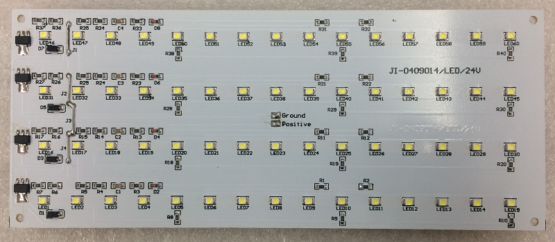
LED PCB Board Design is essential for creating efficient and durable LED lighting solutions. Whether for consumer electronics, automotive applications, or industrial lighting, a well-designed LED Light PCB Circuit Design ensures optimal performance and longevity. With the right PCB Design Service, you can achieve improved heat dissipation, electrical efficiency, and seamless integration of LEDs onto circuit boards. This led pcb design guide will walk you through everything you need to know about LED PCB design, from materials and circuit design to mounting methods and cost considerations.
What is an LED PCB Board?
An LED PCB board is a printed circuit board (PCB) specifically designed to support and power light-emitting diodes (LEDs). Unlike standard PCBs, LED PCBs focus on thermal management since LEDs generate heat, which, if not managed properly, can reduce efficiency and lifespan. Common applications of LED PCB boards include:
LED lighting strips for residential and commercial use
Automotive headlights and dashboards
Medical equipment displays
Smartphones, TVs, and digital billboards
A well-planned LED PCB design ensures even light distribution, durability, and energy efficiency.
What Materials Are Used in LED PCB?
Choosing the right material is crucial for LED PCB circuit design, as it directly affects heat dissipation, durability, and cost. The most commonly used materials are:
1. Aluminum Core PCB
The best choice for high-power LED PCB design
Features a metal core that dissipates heat efficiently
Commonly used in LED strip PCB design and automotive lighting
2. FR-4 (Fiberglass) PCB
A cost-effective choice but requires additional heat dissipation measures
Used in low-power LED applications
3. Ceramic PCB
Offers superior thermal conductivity
Used in high-end LED lighting applications requiring maximum heat resistance
Selecting the right material ensures that LED boards operate efficiently without overheating.
How to Make LED PCB Design?
When working on PCB design for LED light applications, especially for high power LED PCB design, it’s crucial to focus on efficient thermal management and optimized circuit layout to ensure longevity and performance. Proper LED PCB circuit design involves strategic LED placement, adequate heat dissipation, and careful component selection. Specifically, creating a simple LED PCB design involves several key steps:
1. Schematic Design
Use LED PCB design software like Altium Designer, Eagle PCB, or KiCad to create the electrical layout, including:
LED placement
Resistor and capacitor positioning
Power supply routing
2. PCB Layout
Optimize trace width and routing for efficient current flow
Use wide copper traces to prevent overheating
Implement thermal vias for heat dissipation
3. Simulation & Prototyping
Before manufacturing, test the PCB LED design using simulation software to detect issues early.
How to Build a Basic LED Circuit?
A basic LED circuit consists of:
LEDs (Light-emitting diodes)
A power source (battery or DC supply)
Resistors (to limit current and prevent damage)
Wires or PCB traces (to connect components)
Simple LED PCB Design Example
Step 1: Connect the LED anode (+) to the power supply via a resistor.
Step 2: Connect the LED cathode (-) to the ground.
Step 3: Ensure the resistor value matches the LED voltage and current ratings.
This simple circuit is the foundation of LED matrix PCB design, LED driver PCB design, and more.
What is the Width of LED PCB?
The width (thickness) of an LED PCB board depends on its application:
Standard LED PCBs: 1.6mm (most common for general applications)
High-power LED PCBs: 2.0mm – 3.2mm (for better heat dissipation)
Flexible LED PCBs: 0.2mm – 1.0mm (used in LED strips)
The correct PCB width prevents overheating and ensures mechanical stability.
How Do You Mount LEDs on a PCB?
LEDs can be mounted on PCBs using different methods, depending on the design and application:
1. Surface Mount Technology (SMT) – Best for SMD LED PCB Design
Uses solder paste and reflow soldering
Ideal for compact LED light PCB design
2. Through-Hole Technology (THT) – Used for High-Power LEDs
LEDs are inserted into holes and soldered on the other side
Ensures stronger mechanical bonds
3. Chip-on-Board (COB) – Used in LED Matrix PCB Design
LED chips are placed directly on the PCB for high efficiency and compact design
Choosing the right mounting method improves LED performance and durability.
Where Are LED Boards Used?
LED PCBs are found in a wide range of industries due to their energy efficiency and durability. Common applications include:
1. Consumer Electronics
Smartphones, tablets, and TVs
Digital clocks and smart home devices
2. Automotive Industry
Headlights, dashboard displays, brake lights
3. Industrial and Commercial Lighting
LED streetlights, floodlights, warehouse lighting
4. Medical Equipment
LED-based X-ray displays
Surgical lighting and phototherapy devices
These applications highlight why LED PCB circuit design must be robust and customized for each use case.
How Much Does a Custom PCB Board Cost?
The cost of a custom PCB board can vary significantly depending on several factors. The primary considerations include:
Size and Number of Layers: Larger PCBs or those with more layers tend to cost more. For instance, a simple two-layer PCB may cost around $5−$15 per board, while multilayer PCBs are generally more expensive. The specific price needs to be determined based on factors such as the actual design, materials, and process requirements.
Material Type: The choice of material also plays a crucial role. FR-4, a common and cost-effective material, typically costs less than aluminum or ceramic PCBs.
Manufacturing Volume: The quantity produced affects the unit cost. Prototypes and small batches tend to be more expensive due to setup and engineering costs. As the production volume increases, the unit cost decreases, with prices potentially dropping for mass production.
Special Processes and Quality Standards: Additional factors such as surface treatment (e.g., OSP, lead-free soldering, gold plating), copper foil thickness, design complexity, quality inspection standards, mold fees, and testing jigs can further influence the overall cost. Higher-end processes and stricter quality standards will increase the price.
Therefore, for an accurate quotation, it is advisable to consult with a PCB manufacturing service that can provide customized pricing based on your specific project requirements.
In a nutshell, designing an LED PCB board requires careful planning, right material selection, and thermal management strategies. Whether you’re working on a simple LED PCB design, an SMD LED PCB board design, or a high-power LED PCB design, the key to success lies in proper circuit design, component placement, and manufacturing methods.
If you’re looking for expert support, consider a PCB Design Service to streamline your LED light PCB circuit design and ensure the highest quality for your LED projects. With the right LED PCB design software and PCB manufacturing partner, you can create efficient, cost-effective, and long-lasting LED lighting solutions for various applications.
EBest Circuit (Best Technology) offers a full range of Led PCB Board Design, customized to match the unique requirements of each customer. With competitive ODM & OEM pricing, we deliver reliable custom led pcb solutions to support your projects from initial design to final production. For more information or inquiries, feel free to contact EBest Circuit (Best Technology) at sales@bestpcbs.com.
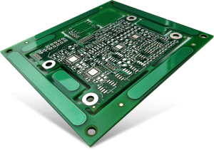
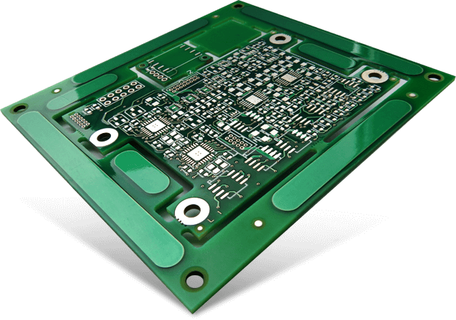
PCB design and fabrication are key steps in producing functional circuit boards for various applications. From simple gadgets to advanced industrial systems, well-designed PCBs ensure performance and reliability. But how does the process work? What factors should designers and manufacturers consider? Let’s dive into the details and uncover the essentials of PCB design and fabrication.
What is the basic rule of PCB design?
Designing a PCB requires precision and adherence to industry best practices. The fundamental rules include:
Component Placement: Place components logically to ensure minimal signal interference and easy routing. Keep high-speed signals short and direct to reduce noise and improve signal integrity. Group related components together to form functional modules for better organization and easier troubleshooting.
Trace Routing: Avoid sharp 90-degree angles to minimize signal reflection and interference; use smooth curves or 45-degree angles instead. Keep trace lengths as short as possible, especially for high-speed signals, to reduce signal degradation. Maintain consistent trace widths to ensure even current distribution and minimize impedance variations.
Power and Ground Planes: Maintain a solid ground plane to improve signal integrity and reduce electromagnetic interference (EMI). Use power planes to provide a stable voltage supply and reduce power distribution impedance. Ensure proper decoupling of power supplies to minimize noise and improve circuit performance.
Thermal Management: Distribute heat-sensitive components wisely to avoid overheating. Incorporate thermal vias and heat sinks as needed to improve heat dissipation.
Spacing and Clearance: Ensure proper spacing between traces to avoid short circuits and maintain electrical performance. Adhere to manufacturer-recommended clearances for components and traces to ensure manufacturability.
Layer Stackup: Choose an appropriate stack-up structure based on the board’s complexity and signal requirements. Properly arrange power planes, ground planes, and signal layers to minimize cross-talk and improve signal integrity.
Impedance Matching: For high-speed signals, ensure transmission lines match the load impedance to reduce signal reflection and loss. Use controlled impedance traces and terminations as needed to maintain signal integrity.
Manufacturability and Testability: Design with ease of manufacturing and testing in mind, such as incorporating test points and following the fabricator’s process requirements. Use standard component packages and footprints to ensure compatibility with automated assembly equipment.
In summary, following these basic rules can help designers create PCBs that are functionally optimized, reliable, and manufacturable. At the same time, designers should also flexibly adjust and optimize their design strategies based on specific application requirements and manufacturing process requirements.
Which tool is used to design PCB?
Several PCB design software tools are available, each offering unique features tailored to different needs. Some of the most widely used tools include:
Altium Designer – Offers an extensive feature set for complex PCB designs and simulation.
Eagle – A popular choice among both beginners and professionals for its intuitive interface.
KiCad – An open-source software that provides flexibility and customization.
OrCAD – Suitable for high-speed and multilayer PCB designs.
Pads PCB – A professional tool ideal for production-oriented PCB layouts.
Choosing the right tool depends on factors such as project complexity, budget, and ease of use.
How do you draw a PCB design?
Creating a PCB design involves multiple stages, each requiring attention to detail:
Schematic Capture: The first step is drawing the schematic diagram, defining electrical connections between components.
Component Selection: Choosing appropriate components based on electrical and thermal requirements.
PCB Layout: Placing components in a way that minimizes signal interference and optimizes performance.
Routing Traces: Connecting components using copper traces while following design rules to maintain proper spacing.
Layer Stackup Design: Defining the number of layers required for signal, power, and ground planes.
DRC (Design Rule Check): Running automated checks to ensure compliance with spacing, trace width, and clearance guidelines.
Gerber File Generation: Preparing files for manufacturing, including drill files, solder mask layers, and assembly instructions.
Following these steps helps achieve a design that is manufacturable and meets performance expectations.
What is the difference between PCB layout and design?
PCB design is the entire process, from conceptualizing the circuit to generating manufacturing files. PCB layout, on the other hand, is a specific step within the design process that focuses on placing components and routing traces. Simply put, design includes planning and simulation, while layout is more about the physical arrangement of components and interconnections.
Concept and Requirements: Define the application, specifications, and constraints.
Schematic Design: Draw the circuit diagram, specifying how components connect.
PCB Layout Design: Place components and route traces while considering signal integrity and thermal management.
Simulation and Testing: Validate the design using software simulations to detect potential issues.
Prototype Fabrication: Manufacture a prototype PCB for testing.
Design Iteration: Make necessary modifications based on testing results.
Final Design Approval: Ensure all aspects meet industry standards before mass production.
A well-planned design process minimizes errors and improves efficiency.
What is the difference between PCB fabrication and manufacturing?
PCB fabrication refers to the process of creating the bare board, which includes etching copper layers, drilling holes, and applying solder masks. PCB manufacturing is a broader term that encompasses fabrication as well as component assembly, soldering, and final testing. In simple terms, fabrication makes the board, while manufacturing completes the final product with all components attached.
What is the difference between PCB fabrication and assembly?
PCB fabrication is the process of building the physical board, while PCB assembly involves placing and soldering components onto the board. Fabrication deals with raw materials and structure, whereas assembly turns the fabricated board into a fully functional circuit.
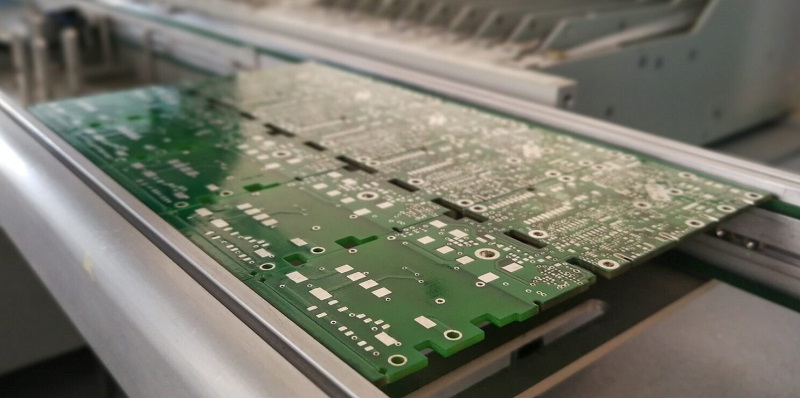
What is the fabrication process in PCB?
The PCB fabrication process consists of multiple steps:
Design Transfer: Convert PCB design files into a format suitable for manufacturing.
Drilling: Create holes for vias and component leads using high-precision drilling machines.
Copper Deposition: Apply copper layers through electroplating or other techniques.
Etching: Remove excess copper to form conductive traces.
Solder Mask Application: Apply a protective layer to prevent oxidation and short circuits.
Silkscreen Printing: Add component labels and markings for easy identification.
Surface Finish Application: Enhance solderability with finishes like HASL, ENIG, or OSP.
Final Inspection: Perform electrical testing and visual inspections to ensure quality.
Each step plays a crucial role in producing a high-performance PCB.
PCB Design and Fabrication Manufacturer
Why choose EBest Circuit (Best Technology) as your PCB design and fabrication manufacturer? Choosing the right partner for PCB design and fabrication is essential for achieving high-quality, reliable, and cost-effective circuit boards. At EBest Circuit (Best Technology), we take pride in delivering top-tier PCB solutions backed by 18 years of expertise, advanced manufacturing capabilities, and customer-centric service. Here’s why we stand out as the ideal choice for your PCB needs.
1. Over 18 Years of PCB Manufacturing Excellence
With nearly two decades in the PCB industry, we understand the intricacies of pcb design and fabrication. Our skilled engineers specialize in layout optimization, signal integrity management, and material selection to enhance PCB performance and durability. Our vast experience allows us to handle everything from designing to large-scale fabrication effortlessly.
2. No Minimum Order Quantity (MOQ)
We cater to all project sizes, whether you need a single prototype for testing or bulk fabrication for mass production. Our flexible approach enables startups and enterprises alike to scale production without compromising quality or efficiency.
3. Fast Turnaround with Reliable Delivery
We recognize the importance of quick time-to-market. Our streamlined production processes ensure PCB delivery within 2-3 weeks, and we offer expedited fabrication options for urgent projects. Our efficient logistics and supply chain management guarantee on-time delivery every time.
3. Cutting-Edge Manufacturing Technology
EBest Circuit (Best Technology) invests in state-of-the-art production facilities and advanced engineering techniques to manufacture high-precision PCBs. Our capabilities include:
High-Density Interconnect (HDI) technology for compact and complex designs.
Laser drilling and fine-line etching for superior accuracy.
Automated Optical Inspection (AOI) and X-ray inspection for defect detection.
Selective wave soldering and precision reflow soldering for robust assemblies.
4. Strict Quality Control and Testing Standards
Quality and reliability are at the core of our PCB fabrication process. We implement rigorous testing procedures to ensure defect-free and high-performance circuit boards. Our quality control measures include:
Electrical Testing (E-Test) to verify circuit continuity.
Impedance Control Analysis for high-frequency applications.
Thermal Stress Testing to evaluate durability under extreme conditions.
Automated and Manual Inspections to maintain consistency and accuracy.
5. Certified PCB Fabrication Facilities
We adhere to global industry standards, ensuring that our PCBs meet the highest levels of quality and compliance. Our certifications include:
6. Expert Technical Support and Engineering Consultation
At EBest Circuit (Best Technology), customer satisfaction is our priority. Our experienced engineers provide end-to-end support, from design consultation and material selection to performance optimization and troubleshooting. If you need assistance with complex PCB design and fabrication, our technical team is available 24/7 to help you achieve the best results.
EBest Circuit (Best Technology) is committed to delivering high-quality PCB design and fabrication services that meet the evolving needs of modern electronics. Our experience, advanced capabilities, and customer-focused approach make us the trusted choice for businesses seeking superior PCB solutions. Whether you’re developing a new product or improving an existing design, we are here to provide expert guidance and manufacturing excellence every step of the way.
In conclusion, understanding PCB design and fabrication is essential for creating durable and efficient circuit boards. By following best practices, using the right tools, and ensuring proper fabrication processes, high-quality PCBs can be produced. If you’re looking for a trusted partner in PCB design, fabrication, and assembly, EBest Circuit (Best Technology) offers over 18 years of expertise in delivering top-notch PCBs. Feel free to contact us at sales@bestpcbs.com for any doubts or queries you might have.
A circuit card is the backbone of any electronic device, providing a structured platform for electrical components to function seamlessly. Whether in consumer electronics, automotive systems, medical devices, or aerospace applications, circuit cards enable efficient signal transmission and power distribution. Understanding circuit card design, materials, prototyping, and manufacturing processes is crucial for producing high-quality electronic products. This guide explores the key aspects of circuit card development, from design considerations to final assembly, helping engineers and manufacturers optimize their processes.
What is a Circuit Card?
A circuit card is an electronic board that houses and connects various electrical components. It consists of a substrate, conductive traces, and mounted components like resistors, capacitors, and integrated circuits. Circuit cards are used in virtually every electronic device, ensuring signal integrity and efficient functionality. Unlike traditional wiring methods, they provide a compact and stable solution for electronic designs.
What Are the Different Types of Circuit Cards?
1. Classification by Structure Single-Sided Circuit Card A single-sided circuit card has conductive traces on only one side of the substrate. Components are mounted on one surface, making it a cost-effective solution for simple electronic devices like calculators, power supplies, and LED lighting.
Double-Sided Circuit Card A double-sided circuit card features conductive layers on both sides of the substrate, connected through vias. This design improves circuit density and functionality, making it suitable for industrial controls, power management, and communication devices.
Multilayer Circuit Card A multilayer circuit card consists of three or more layers of conductive material stacked together. These layers are insulated from each other by dielectric materials and connected through plated vias. High-density integration, reduced electromagnetic interference (EMI), and improved performance make multilayer cards ideal for high-speed computing, 5G networks, and aerospace electronics.
Rigid Circuit Card A rigid circuit card is built on solid substrates such as FR4 (fiberglass epoxy), aluminum, or ceramic. It provides structural stability and durability, making it suitable for automotive electronics, industrial automation, and medical equipment.
Flexible Circuit Card A flexible circuit card is made from polyimide (PI) or polyester (PET) materials, allowing it to bend and fold without damage. These cards are used in wearable devices, smartphones, and compact electronics where space-saving and durability are essential.
Rigid-Flex Circuit Card A rigid-flex circuit card combines rigid and flexible sections in a single board. This hybrid design enhances mechanical stability and electrical reliability, making it suitable for military avionics, medical implants, and robotics.
2. Classification by Function and Application Processing & Control Circuit Cards These circuit cards act as the brain of electronic systems, handling computations and control tasks.
Motherboards – Found in computers, industrial control systems, and embedded computing.
GPU Cards – Used in graphics processing, AI computations, and gaming systems.
FPGA/ASIC Accelerator Cards – Custom computing solutions for AI inference, video processing, and financial modeling.
Storage Circuit Cards Storage-related circuit cards are responsible for data retention and high-speed access.
Memory Modules (DRAM, SRAM) – Installed in computers and servers for fast data processing.
Solid-State Drive (SSD) Control Boards – Manage data storage, encryption, and read/write operations in SSDs.
Communication Circuit Cards These circuit cards facilitate data transmission and wireless communication.
RF Circuit Cards (Wi-Fi, Bluetooth, Radar Modules) – Used in IoT devices, automotive radar, and wireless communication systems.
Interface & Expansion Circuit Cards These cards expand device capabilities and enable connections between peripherals.
PCIe Expansion Cards – Used for data acquisition, sound processing, and graphics rendering.
Signal Conversion Boards (USB, HDMI, DisplayPort) – Convert signals for different display and connectivity standards.
Power Management Circuit Cards These circuit cards regulate voltage and power distribution for various applications.
Power Distribution Boards (PDN) – Found in data centers, industrial machinery, and energy storage systems.
Inverter Control Boards (DC-AC Conversion) – Used in solar power systems, electric vehicles, and motor drives.
Sensor & Actuator Circuit Cards These cards process sensor inputs and control actuators in automation and robotics.
Sensor Interface Boards – Used in temperature, pressure, and image acquisition systems.
Motor Driver Boards – Control stepper motors, servo systems, and robotic actuators.
Choosing the appropriate circuit card depends on design complexity, performance requirements, and environmental conditions. Whether you need high-speed processing, rugged durability, or flexible designs, selecting the right type is crucial for achieving optimal system performance.
At EBest Circuit (Best Technology), we specialize in custom circuit card solutions, offering advanced manufacturing, precise engineering, and expert consultation to meet your project’s unique requirements.
What Materials Are Used to Make Circuit Cards?
Selecting the right materials is crucial for a circuit card’s durability and performance. Common materials include:
FR4 (Fiberglass Epoxy) – Offers good insulation, mechanical strength, and cost-effectiveness.
Polyimide – Used in flexible circuit cards for its heat resistance and flexibility.
Metal Core (Aluminum or Copper) – Enhances heat dissipation in high-power applications.
Ceramic Substrates – Provides excellent thermal and electrical stability for high-frequency designs.
Circuit Card Design
How to design a circuit card? Designing a circuit card requires precision and careful planning. The key steps include:
Define Requirements – Determine the circuit’s function, power needs, and layout constraints.
Create a Schematic – Develop a blueprint showing the electrical connections between components.
Select Components – Choose resistors, capacitors, ICs, and other parts based on application needs.
Design PCB Layout – Arrange components and route traces to ensure signal integrity and thermal efficiency.
Simulate and Validate – Test the design virtually before creating a circuit card prototype.
Prototype and Test – Build an initial version and conduct performance testing before mass production.
What Are the Benefits of a Circuit Card?
Circuit cards offer numerous advantages in electronic design and manufacturing:
Compact and Lightweight – Saves space while maintaining high functionality.
Improved Electrical Performance – Ensures stable signal transmission and power distribution.
Cost-Effective Manufacturing – Supports mass production with minimal errors.
Scalability – Allows easy modification for different applications.
What Are the Applications of Circuit Cards?
Circuit cards are integral to a wide range of industries:
Consumer Electronics – Found in smartphones, computers, and home appliances.
Automotive Systems – Used in engine controls, infotainment, and safety systems.
Medical Devices – Enables precision in imaging systems, diagnostic tools, and monitoring equipment.
Aerospace and Defense – Provides reliability for avionics, satellites, and military equipment.
Industrial Automation – Supports robotics, sensors, and control systems.
Circuit Card Manufacturer
Why choose EBest Circuit (Best Technology) as your circuit card manufacturer? Choosing the right circuit card manufacturers is critical to ensuring product reliability, performance, and long-term success. At EBest Circuit (Best Technology), we go beyond basic manufacturing to offer comprehensive, high-quality solutions tailored to your exact needs. Here’s why we are the preferred choice for circuit card design, prototyping, and mass production.
1. Full Turnkey Circuit Card Solutions
We provide end-to-end circuit card services, from initial design and prototyping to full-scale production. Whether you need a standard circuit card or a customized solution optimized for complex layouts, high-speed signals, or extreme environments, our team ensures seamless development at every stage.
2. Over 18 Years of Manufacturing Excellence
With nearly two decades of expertise, we understand the challenges of modern electronics manufacturing. Our in-house engineers specialize in material selection, layout optimization, and high-precision circuit card assembly to deliver superior circuit card performance. Our extensive experience allows us to handle high-frequency, high-power, and multi-layer designs with ease.
3. No Minimum Order Quantity (MOQ) Requirement
We support projects of any scale—from small prototype batches for testing to large-volume production for mass deployment. Our flexible manufacturing approach allows you to scale production as needed while maintaining consistent quality at every stage.
4. Certified Manufacturing Facilities for Global Standards
We adhere to strict industry certifications to meet the highest quality and safety standards. Our manufacturing facilities comply with:
ISO 9001 – Quality Management System
ISO 13485 – Medical Device Manufacturing Standard
IATF 16949 – Automotive Industry Standard
AS9100D – Aerospace Industry Certification
RoHS & REACH Compliance – Environmentally Friendly Production
5. Industry-Specific Expertise & Customization
Each industry has unique requirements, and we tailor our solutions to match specific applications, including:
Automotive Electronics – High-reliability circuit cards for vehicle control systems.
Medical Devices – Precision circuits for imaging, diagnostics, and monitoring.
Industrial Automation – Custom solutions for robotics, control systems, and sensors.
6. Dedicated Technical Support & Engineering Consultation
Our customer-first approach means that you receive expert guidance at every stage. Whether you need design assistance, performance optimization, or troubleshooting, our experienced engineers are available 24/7 to provide technical support and consultation.
FAQs Of Circuit Card
1. What Does a Circuit Card Do?
A circuit card connects and supports electronic components, allowing signals and power to flow efficiently between them. It acts as the foundation for any electronic system, ensuring stable operation.
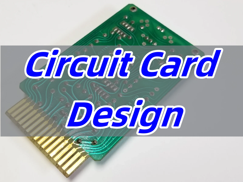
2. What is the Difference Between a Circuit Card and a PCB?
A circuit card is a complete electronic assembly that includes a printed circuit board (PCB) and mounted components. A PCB is just the bare board before component placement.
3. How Does a Circuit Card Work?
A circuit card works by transmitting electrical signals through its copper traces, enabling communication between different electronic components. This controlled flow allows the device to perform specific functions.
4. How Do You Use a Circuit Card?
Circuit cards are integrated into electronic devices during the assembly process. They are placed inside enclosures, connected to other systems, and powered to perform designated tasks.
In a nutshell, a well-designed circuit card is essential for reliable and efficient electronics. From material selection to assembly, every stage plays a crucial role in ensuring performance and durability. If you need expert guidance, EBest Circuit (Best Technology) offers high-quality circuit card solutions tailored to your requirements. Reach out to us at sales@bestpcbs.com for more details.
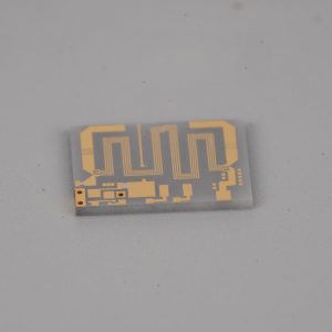
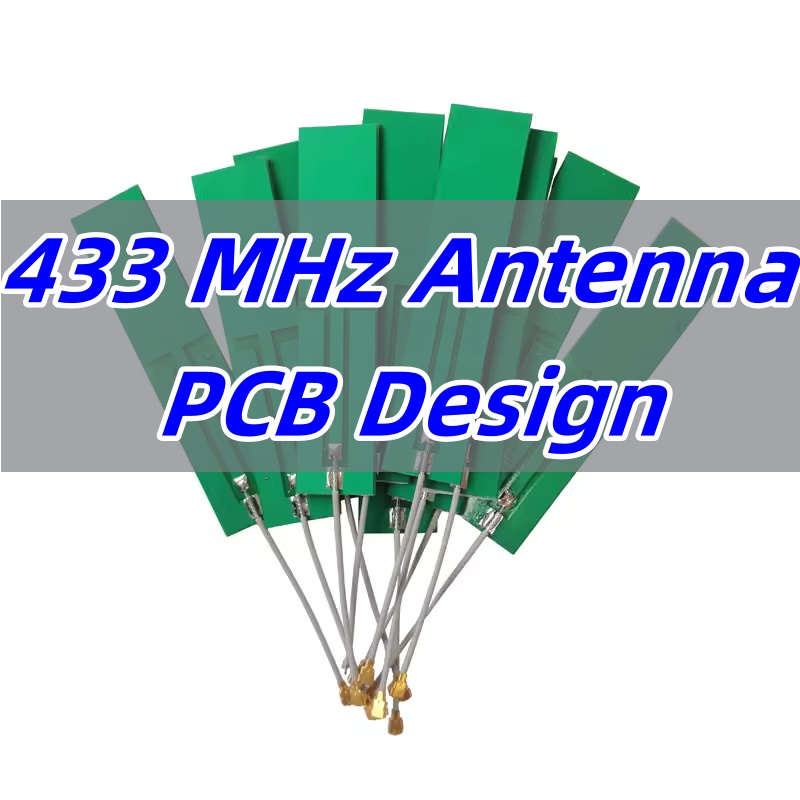
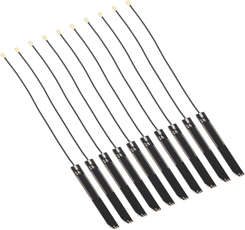
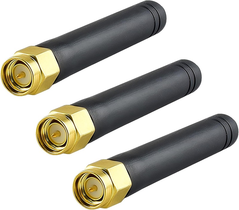
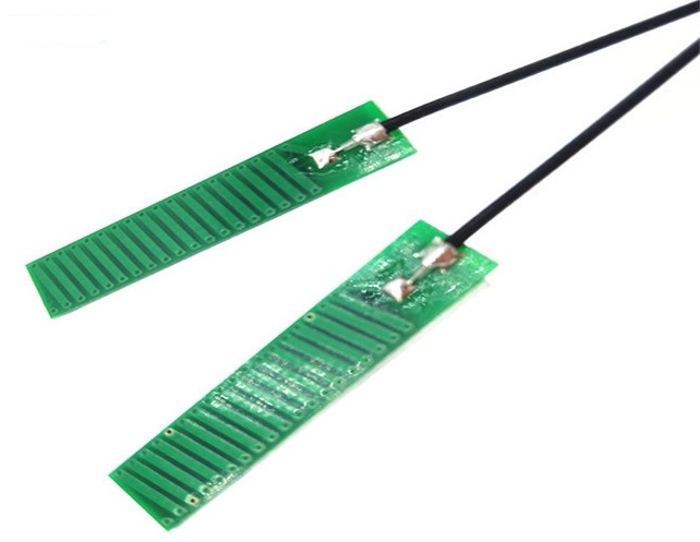
433 MHz antenna performance depends on high-quality PCB design and manufacturing. Choosing the right supplier ensures stable signal transmission, durability, and efficiency. At EBest Circuit (Best Technology), we specialize in designing and producing 433 MHz antenna PCBs, offering full turn-key solutions, strict quality control, and fast delivery. With our extensive experience, advanced facilities, and customer-focused approach, we are your trusted partner for reliable wireless communication solutions.
What is a 433 MHz antenna?
A 433 MHz antenna is a specialized antenna that operates at a frequency of 433 MHz, commonly used in wireless communication systems. It helps transmit and receive radio signals efficiently over a specific range. This frequency is widely used in applications like remote controls, IoT devices, LoRa modules, and wireless sensor networks. The right antenna design improves signal strength, transmission stability, and overall communication efficiency.
What Are the Different Types of 433 MHz Antennas?
433 MHz antennas come in various designs, each optimized for specific applications. They can be categorized based on directionality, physical structure, installation method, and application scenarios. Selecting the right 433 MHz antenna ensures stable signal transmission and optimal performance for wireless communication systems.
1. Classification by Directionality
Omnidirectional 433 MHz Antennas
Omnidirectional antennas radiate signals evenly in all directions, similar to a light bulb. They are ideal for applications where signals need to be transmitted across a wide area, such as smart home hubs, wireless sensor networks, and IoT devices. Examples: Rubber duck antennas, monopole antennas.
Directional 433 MHz Antennas
These antennas focus signals in a specific direction, improving transmission distance and minimizing interference. They are commonly used for long-range, point-to-point communication where signal strength and efficiency are critical. Examples: Yagi antennas, panel antennas.
2. Classification by Physical Structure
Wire-Type (Whip) 433 MHz Antennas
Antennas composed of a single conductive wire, characterized by simplicity and mechanical flexibility. At 433 MHz, their physical length is typically designed as a quarter-wavelength (λ/4 ≈17.3 cm) to achieve impedance matching and resonance. Monopole variants require a ground plane (e.g., PCB copper layer or metallic chassis) to complete the current return path.
They are commonly used for low-cost wireless remote controls (e.g., garage door openers), embedded systems (for concealed antenna integration), and rapid prototyping of RF circuits. Examples: Straight wire antennas, monopole whip antennas.
Helical 433 MHz Antennas
These antennas have a coiled structure, offering compact size with improved gain. They are widely used in IoT devices, RFID tags, and embedded wireless modules where space-saving is crucial. Examples: Helical spring antennas, compact coil antennas.
Loop 433 MHz Antennas
Loop antennas use a closed-loop structure to enhance efficiency in near-field communication. They are particularly effective in RFID systems and short-range wireless applications. Examples: Small circular loop antennas, ferrite-core loop antennas.
Dipole 433 MHz Antennas
Dipole antennas consist of two equal-length conductive elements, offering balanced performance with stable impedance. These antennas are commonly used in wireless communication systems where consistent signal reception is necessary. Examples: Half-wave dipole antennas, folded dipole antennas.
PCB 433 MHz Antennas
PCB antennas are directly integrated into circuit boards, providing a cost-effective and space-efficient solution for compact wireless devices. These antennas are widely used in IoT applications, remote controls, and embedded systems. Examples: Microstrip PCB antennas, inverted-F PCB antennas.
3. Classification by Installation Method
Internal 433 MHz Antennas
Built into the device, internal antennas save space while maintaining a sleek design. They are commonly used in wearables, smart sensors, and compact wireless modules where external antennas are not practical. Examples: PCB antennas, flexible FPC antennas.
External 433 MHz Antennas
External antennas can be adjusted or replaced to optimize signal performance. They offer better gain and extended range for industrial automation, remote control systems, and telemetry applications. Examples: SMA connector antennas, magnetic base antennas.
Retractable 433 MHz Antennas
These antennas can be extended for better signal reception or retracted for portability. They are commonly found in handheld radios, walkie-talkies, and vehicle-mounted communication systems. Examples: Telescopic antennas, extendable whip antennas.
4. Classification by Application Scenario
Industrial-Grade 433 MHz Antennas
Designed for harsh environments, these antennas feature enhanced durability, waterproofing, and resistance to electromagnetic interference. They are widely used in industrial IoT, machine-to-machine communication, and telemetry systems. Examples: Heavy-duty whip antennas, weatherproof outdoor antennas.
Consumer-Grade 433 MHz Antennas
These antennas are compact and cost-effective, making them suitable for everyday consumer electronics such as remote controls, smart home devices, and wireless doorbells. Examples: Spring antennas in remotes, embedded chip antennas in smart home devices.
Special-Purpose 433 MHz Antennas
Custom-designed for specialized applications, these antennas are used in military communication, satellite tracking, and ultra-long-range data transmission. Examples: High-gain directional Yagi antennas, military-grade helical antennas.
433 MHz antennas come in a variety of designs, each tailored for specific needs. Choosing the right 433 MHz antenna depends on signal range, installation method, and operating environment. Whether used for IoT applications, industrial automation, or long-range wireless communication, the proper antenna selection ensures stable and efficient performance.
What materials are used to make 433 MHz antennas?
The materials used in 433 MHz antennas impact performance, durability, and signal efficiency. Common materials include:
Copper: Excellent conductivity, used in PCB traces and wire antennas.
Brass: Often used in connectors and high-frequency antennas due to its strength.
Steel: Provides durability but has lower conductivity than copper.
FR4 (PCB Material): Common substrate for PCB antennas, balancing cost and performance.
Ceramic: Used in high-performance chip antennas for compact designs.
The choice of material depends on factors like cost, efficiency, and intended use.
433 MHz Antenna Design
How to design a 433 MHz antenna? Designing a 433 MHz antenna involves careful consideration of frequency tuning, impedance matching, and size optimization. The key steps include:
Determine the Antenna Length: The ideal length is based on the wavelength (λ) at 433 MHz, typically around 17.3 cm for a quarter-wave antenna.
Choose the Antenna Type: Decide between a PCB, wire, or external antenna based on application needs.
Optimize the PCB Layout: If designing a PCB antenna, maintain proper ground plane design and impedance matching to 50Ω for efficient signal transfer.
Use Matching Networks: Components like capacitors and inductors help tune the antenna to minimize signal loss.
Test and Adjust: Use tools like vector network analyzers (VNA) to fine-tune performance and achieve maximum signal efficiency.
A well-designed antenna enhances communication range, reduces interference, and improves device reliability. As a leading 433 MHz antenna PCB manufacturer, EBest Circuit (Best Technology) specializes in 433 MHz antenna PCB design, providing high-performance solutions for reliable wireless communication.
What are the benefits of a 433 MHz antenna?
Using a 433 MHz antenna offers several advantages in wireless applications:
Longer Range: Compared to higher frequencies, 433 MHz signals travel farther with lower power.
Better Penetration: Signals can pass through walls and obstacles more effectively.
Low Power Consumption: Ideal for battery-powered devices, ensuring extended operation.
Reliable Performance: Stable connectivity for IoT, remote control, and industrial systems.
Cost-Effective: Simple design and widely available components keep costs low.
These benefits make 433 MHz antennas a preferred choice for various wireless systems.
What are the applications of 433 MHz antennas?
433 MHz antennas are widely used in multiple industries, including:
Remote Controls: Used in car key fobs, garage doors, and security systems.
IoT and Smart Devices: Wireless communication for smart homes, meters, and automation systems.
LoRa and RF Modules: Key components in long-range, low-power wireless communication networks.
Industrial Automation: Reliable connectivity in factories and logistics tracking.
Drones and RC Equipment: Enhancing signal stability for remote-controlled devices.
Their versatility makes them an essential part of modern communication technology.
433 MHz antenna PCB manufacturer
Why choose EBest Circuit (Best Technology) as your 433 MHz antenna PCB manufacturer? When selecting a 433 MHz antenna PCB manufacturer, you need more than just a supplier—you need a reliable partner with industry expertise, technical precision, and a commitment to quality. At EBest Circuit (Best Technology), we go beyond manufacturing; we deliver tailored solutions to ensure superior performance, durability, and reliability. Here’s why companies worldwide trust us for their 433 MHz antenna PCB needs:
EBest Circuit (Best Technology) offers more than just PCBs—we work with you from design to final production. Whether you require a standard 433 MHz antenna PCB or a customized solution optimized for device size, signal strength, and environmental conditions, we provide end-to-end support to ensure optimal performance.
2. Over 18 Years of PCB Manufacturing Expertise
With nearly two decades of experience, our team understands the critical role an antenna PCB plays in wireless communication systems. We manage the entire design and production process in-house, ensuring precise material selection, layout optimization, and signal tuning to deliver maximum efficiency for your 433 MHz applications.
3. No Minimum Order Quantity (MOQ) Requirement
Flexibility is key to innovation. Whether you need a small prototype batch for testing or mass production for large-scale deployment, we accommodate orders of any size. Our no MOQ policy allows you to scale production at your pace while ensuring high-quality results.
4. Fast and Reliable Delivery: 2-3 Weeks Lead Time
We understand that timely delivery is crucial for your projects. With our streamlined production process, we deliver 433 MHz antenna PCBs within 2-3 weeks, helping you stay on schedule without sacrificing quality.
5. Superior Quality Assurance
Wireless performance depends on precision and reliability. Every 433 MHz antenna PCB manufactured by EBest Circuit (Best Technology) undergoes rigorous testing to meet frequency accuracy, gain stability, and long-term durability standards. Our commitment to quality ensures flawless signal transmission and extended product life.
6. Certified Manufacturing Facilities
We operate under globally recognized quality standards, ensuring compliance with multiple industries, including medical, automotive, and aerospace applications:
ISO 13485 (Medical Device Standard)
IATF 16949 (Automotive Industry Standard)
AS9100D (Aerospace Industry Standard)
7. Customer-Focused Technical Support
Every industry has unique wireless challenges. Whether you’re developing IoT devices, industrial automation systems, remote-control applications, or telemetry solutions, our team offers specialized expertise to meet your specific requirements. Our PCB engineers provide 24/7 consultation, ensuring you receive the best technical guidance and support.
Choosing the right 433 MHz antenna PCB manufacturer is essential for reliable and efficient wireless communication. With our industry-leading expertise, cutting-edge facilities, and strict quality control, EBest Circuit (Best Technology) is your trusted partner for custom and standard antenna PCB solutions. Just feel free to get in touch with us at sales@bestpcbs.com to discuss your project requirements together!
FAQs of 433 MHz Antenna
1. What is the range of a 433 MHz antenna?
The range depends on the antenna type, environment, and power output. In open spaces, a 433 MHz antenna can reach 100–150 meters with a basic setup, while high-gain directional antennas can extend this to several kilometers.
2. What is the best length for a 433 MHz antenna?
For optimal performance, a quarter-wave antenna should be 17.3 cm, while a half-wave antenna measures 34.6 cm. Proper tuning and impedance matching enhance signal efficiency.
3. Why is 433 MHz so popular?
433 MHz is widely used due to its long-range capabilities, low power consumption, and strong penetration through obstacles. It is also license-free in many regions, making it ideal for IoT, security, and industrial applications.
4. How to make a 315/433 MHz RF antenna?
To build a basic 433 MHz wire antenna, follow these steps:
Cut a copper wire to 17.3 cm for a quarter-wave antenna.
Solder one end to the RF module’s antenna pad.
Ensure proper grounding for stability.
Use a heat shrink or protective casing for durability.
Fine-tuning with a matching network can improve efficiency.
5. Will a 433 MHz antenna work for cellular?
No, 433 MHz antennas are not suitable for cellular networks since cellular frequencies range from 700 MHz to 2600 MHz. A proper antenna designed for cellular bands is required.
6. Will a 433 MHz antenna work for GSM?
No, GSM networks operate at 850 MHz, 900 MHz, 1800 MHz, and 1900 MHz. A 433 MHz antenna will not function correctly for GSM applications.
In conclusion, 433 MHz antenna plays a crucial role in wireless communication, offering reliable performance in various applications. Choosing the right design and manufacturer enhances efficiency and connectivity. EBest Circuit (Best Technology) provides top-quality 433 MHz antennas tailored to meet industry needs. For professional 433 MHz antenna PCB solutions, feel free to contact EBest Circuit (Best Technology) at sales@bestpcbs.com. Our team is always ready to assist you!
2.4 GHz antenna plays a key role in wireless communication today. From WiFi routers to smart home devices, they keep us connected without messy cables. Whether you need reliable coverage for short-range indoor use or long-range outdoor connections, the right 2.4 GHz antenna can improve your system’s performance. EBest Circuit (Best Technology) handle both design and production for 2.4Ghz antenna PCB, we can optimize performance from the start. When you need reliable 2.4 GHz antenna PCB, EBest Circuit (Best Technology) delivers top-quality solutions tailored to your project.
What is a 2.4 GHz Antenna?
A 2.4 GHz antenna is a specialized antenna that operates within the 2.4 GHz frequency band. This frequency is widely used for wireless technologies like WiFi, Bluetooth, and IoT devices.
Because 2.4 GHz antennas work within this popular band, they support many devices and systems. Whether for indoor use or longer outdoor coverage, they can send and receive signals efficiently. Their design focuses on matching frequency requirements while balancing gain, size, and range.
What Are the Different Types of 2.4 GHz Antennas?
There are several 2.4 GHz antenna types designed for different environments and needs. Each type offers distinct features to match specific wireless setups.
1. By Radiation Pattern
Omnidirectional Antennas
Omnidirectional antennas send signals in all directions. Radiate signals in all directions horizontally, like ripples on water. They are ideal for indoor WiFi routers or small IoT devices where full-area coverage matters most. (e.g., Wi-Fi routers, smart speakers).
Directional Antennas
Directional antennas focus energy in one direction to boost signal strength over longer distances. Focus energy like a flashlight beam. These are perfect for point-to-point outdoor links, long-distance links (e.g., outdoor cameras, wireless bridges).
2. By Integration Method
PCB Antennas
PCB Antennas are designed as copper traces embedded directly into circuit boards. Ideal for mass-produced devices due to low cost and space-saving design. Common in Bluetooth earphones, smart thermostats, and IoT sensors. Their performance depends on board material (e.g., FR4 for basic needs, Rogers substrates for high-frequency stability). Requires precise impedance matching to avoid signal loss.
Flexible Antennas
Flexible Antennas are made with thin, bendable materials like polyimide film or flexible printed circuits (FPC). Withstands repeated bending, making them perfect for wearables (e.g., fitness bands) or devices with curved surfaces (e.g., medical patches). Some models survive 100,000+ bend cycles. Water-resistant options available for outdoor gear.
3. By Installation Location
Internal Antennas
Integrated within the device housing, optimized for compact designs and aesthetic concealment. Common in consumer electronics (e.g., smartphones, smartwatches) where space and design are critical. Typically use PCB or flexible antennas for seamless integration
External Antennas
Mounted outside the device via connectors (e.g., SMA) or cables, enabling flexible placement for optimal signal reception. Ideal for environments requiring tunable orientation or signal amplification (e.g., industrial routers, drones). High-gain directional variants (e.g., Yagi-Uda) are often external for long-range applications.
The reason 2.4GHz antennas widely adopt SMA connectors is threefold:
Superior high-frequency performance – low loss (<0.1 dB @ 2.4GHz) and stable 50Ω impedance up to 18GHz;
Robust mechanical design – compact threaded interface ensuring durability in space-constrained devices like drones;
Regulatory compliance – standardized variants (e.g., RP-SMA) meet FCC/CE certifications for Wi-Fi routers and IoT equipment.
SMA Connector has gender identification. Most antennas use female SMA connectors (hole), while devices (e.g., routers) use male SMA ports (pin). SMA Connector Gender Identification:
SMA Male (Plug): Features a center pin and inner threads.
SMA Female (Jack): Has a center hole and outer threads.
Reverse-polarity SMA (RP-SMA) swaps genders, common in Wi-Fi gear. Pls always check device specs to avoid mismatches.
What Materials Are 2.4 GHz Antennas Made Of?
The materials used to build a 2.4 GHz antenna directly affect how well it performs, how long it lasts, and how easy it is to fit into different devices. Choosing the right materials helps balance conductivity, weight, cost, and durability. Let’s break down the most common material choices and where they fit best.
1. Conductive Metals for High Signal Efficiency
The main goal of any 2.4 GHz antenna is to efficiently radiate and receive signals, so the core material must conduct electricity well.
Copper is one of the top choices. Its excellent conductivity helps signals pass through with minimal loss, which directly improves antenna efficiency. Copper is widely used in both external and internal antennas, particularly in applications where high performance is critical.
Aluminum offers another option, especially for larger antennas where weight savings are important. Although aluminum’s conductivity is lower than copper’s, it’s still good enough for many 2.4 GHz antenna applications, especially directional designs like Yagi antennas or outdoor panels.
These metals form the main radiating elements in most antennas, whether they’re external, internal, or PCB-based.
2. Ceramic for Compact Embedded Designs
When devices shrink, so do their antennas. Many modern devices rely on ceramic antennas, especially for built-in 2.4 GHz antenna PCB layouts.
Ceramic materials allow antennas to stay small without losing too much performance.
They handle higher frequencies like 2.4 GHz well, making them perfect for compact gadgets such as IoT sensors, smart home devices, fitness trackers, and smartphones.
Ceramic antennas are often printed directly onto the PCB or mounted as small components. Their high dielectric constant helps keep the physical size small while still maintaining reasonable performance.
3. Protective Coatings and Weatherproof Materials
For outdoor applications, 2.4 GHz antennas face a different challenge—exposure to sun, rain, and extreme temperatures. Materials used in these antennas need to survive tough conditions without affecting performance.
Many outdoor antennas use weather-resistant plastics to cover the metal radiators. This plastic shielding blocks moisture and dirt but allows radio signals to pass through with minimal interference.
In harsher industrial or marine settings, UV-resistant coatings and corrosion-resistant metals add extra protection, keeping antennas working reliably for years.
These protective materials make sure outdoor antennas can handle long-term exposure while still providing stable connections, even in challenging environments.
2.4 GHz Antenna Design
How to design a 2.4 GHz antenna? Designing a 2.4 GHz antenna may look simple on the surface, but every step directly affects how well the antenna performs. Engineers focus on balancing frequency, size, gain, and impedance matching to get the best signal strength and stable connection. Below is a clear step-by-step breakdown of the key stages.
1. Selecting the Right Antenna Type and Length
The first step in the design process is deciding which 2.4 GHz antenna type works best for the device and its application. Common options include omnidirectional antennas, directional antennas, and PCB-integrated antennas.
Omnidirectional antennas radiate signals evenly in all directions, which suits routers, smart home devices, and wireless cameras.
Directional antennas focus the signal in one direction, which helps with long-range connections or point-to-point communication.
PCB antennas fit directly onto the circuit board, making them perfect for compact gadgets like wearables and IoT devices.
Once the type is clear, the 2.4 GHz antenna length becomes critical. For 2.4 GHz signals, a quarter-wavelength antenna is roughly 31 mm, while half-wavelength antennas are about 62 mm. These values shift slightly depending on the design and placement, especially in small or embedded products. Keeping the length correct ensures the antenna resonates properly at 2.4 GHz, which directly impacts performance.
2. Shaping the Antenna and Optimizing Radiation Pattern
The next important part is choosing the antenna shape since it directly affects how the antenna radiates signals. Different shapes suit different needs:
Helical antennas (coiled wire designs) work well when space is extremely limited. Despite the compact form, they still deliver usable performance.
Patch antennas, often seen in routers and access points, offer reliable coverage with a relatively small footprint.
Monopole or dipole antennas strike a balance between size and performance, making them versatile for indoor and outdoor devices.
Once the shape is selected, engineers use simulation software to model how the antenna radiates at 2.4 GHz. These simulations reveal weak points, dead zones, or unexpected reflections that could weaken signal strength. The design can be adjusted to boost coverage, reduce interference, and fine-tune the antenna’s radiation pattern.
3. Ensuring Proper Impedance Matching and Minimizing Interference
With the physical design in place, attention shifts to impedance matching—a critical factor for signal transfer efficiency. The 2.4 GHz antenna must match the output impedance of the connected device, typically 50 ohms. A mismatch causes signal reflections, which lower efficiency and reduce range.
The antenna materials, trace width, and even the 2.4 GHz antenna PCB layout all affect impedance. Engineers adjust these factors during prototyping to get the cleanest match possible.
Finally, interference checks are essential. The 2.4 GHz band is crowded, with Wi-Fi, Bluetooth, and countless smart devices all sharing the same space. Good antenna designs use filtering techniques, proper shielding, and smart placement to reduce noise from nearby electronics. By minimizing interference, the antenna delivers cleaner signals and better reliability, especially in busy environments like homes and offices.
EBest Circuit (Best Technology) offers a full range of high-quality antenna PCBs, customized to match the unique requirements of each customer. With competitive ODM & OEM pricing, we deliver reliable 2.4 GHz antenna solutions to support your projects from initial design to final production.
What Are the Benefits of 2.4 GHz Antennas?
The 2.4 GHz antenna stands out in the wireless world thanks to its strong performance across various devices and environments. Its advantages explain why it plays such a key role in modern communication systems. Let’s break down some of the key benefits.
1. Compatibility Across Multiple Technologies
One of the biggest benefits of a 2.4 GHz antenna is its broad compatibility. It works smoothly with popular wireless standards like WiFi, Bluetooth, Zigbee, and proprietary RF systems.
This flexibility allows engineers to create devices that communicate across homes, offices, factories, and even outdoor spaces—all using the same frequency band. Because so many devices operate at 2.4 GHz, businesses and designers can standardize around this frequency, reducing complexity when building connected systems.
2. Longer Range Compared to Higher Frequencies
Another key advantage is range. Compared to higher bands like 5 GHz, the 2.4 GHz antenna supports better signal penetration and wider coverage.
Signals at 2.4 GHz travel farther, especially indoors where walls, furniture, and other obstacles can block higher frequencies. This longer range is valuable for applications like smart homes, industrial sensors, and outdoor IoT systems where stable connections matter more than speed.
This is why 2.4 GHz antennas remain so popular, even though faster frequencies exist.
3. Flexible Designs for Every Application
The 2.4 GHz antenna can be designed to match almost any requirement.
For compact devices like wearables or sensors, tiny PCB antennas fit directly onto circuit boards without adding bulk.
For outdoor or long-distance uses, larger high-gain directional antennas focus signals in a specific direction to improve coverage and signal strength.
This range of options—from small embedded antennas to large external ones—gives designers freedom to choose the perfect antenna for each product.
What Are the Applications of 2.4 GHz Antennas?
Because the 2.4 GHz antenna combines wide compatibility, reliable range, and flexible designs, it fits into countless industries and use cases. From home networks to industrial automation, this frequency keeps devices connected in every corner of life.
1. Smart Homes and Consumer Electronics
In residential settings, 2.4 GHz antennas power the everyday devices people rely on.
WiFi routers use 2.4 GHz to provide whole-home coverage, especially in multi-story homes where walls and floors block higher frequencies.
Smart TVs, security cameras, smart plugs, and speakers also connect using this band, ensuring devices stay linked to home networks without constant dropouts.
Even smaller gadgets like smart thermostats, light switches, and door sensors all benefit from the reliability of 2.4 GHz antennas.
2. Industrial and Agricultural Systems
Beyond homes, 2.4 GHz antennas support critical wireless links in factories, warehouses, and farms.
In industrial automation, machines rely on 2.4 GHz wireless connections to report performance data and receive remote commands.
In smart agriculture, wireless soil sensors, irrigation controllers, and livestock trackers all depend on 2.4 GHz antennas to transmit data across fields and greenhouses.
These industries value 2.4 GHz for its range, penetration, and low power requirements, making it ideal for sprawling facilities and remote locations.
3. Automotive and Healthcare Technologies
The automotive and medical sectors also take advantage of 2.4 GHz antennas in innovative ways.
Connected vehicles use them to communicate with roadside sensors, smart traffic lights, or other vehicles nearby.
In healthcare, patient monitors, wearable health trackers, and wireless diagnostic tools rely on 2.4 GHz to continuously transmit data to caregivers without using wired connections.
Because 2.4 GHz antennas balance reliable performance and compact size, they work perfectly in cars and medical devices where space and reliability matter most.
2.4 GHz Antenna PCB Manufacturer
Why choose EBest Circuit (Best Technology) as your trusted 2.4 GHz antenna PCB manufacturer? When choosing a 2.4 GHz antenna PCB manufacturer, you want more than just a product — you need a partner who understands your industry, your project requirements, and your timeline. At EBest Circuit (Best Technology), we deliver all that and more. Here’s why companies worldwide trust us for their 2.4 GHz antenna needs:
1. Full Turn-key Antenna PCB Solutions
At EBest Circuit (Best Technology), we do more than supply antennas PCB — we work alongside you from initial design all the way to final delivery. Whether you need a standard design or something fully customized to match your device size, operating environment, and signal requirements, we’ve got you covered.
2. 18 Years PCB Manufacturing Experience
With over 18 years of hands-on experience in PCB manufacturing, our engineering team ensures your antenna’s performance is fine-tuned from the start. By handling both design and production under one roof, we make sure every detail — from material selection to layout optimization — works in harmony to maximize performance.
3. No MOQ Requirement
We also provide flexible order sizes, whether you need a small prototype batch for testing or high-volume production for mass deployment. With no MOQ restrictions, we ensure rapid turnaround times and dedicated support for projects of any scale.
4. 2-3 Weeks Fast Delivery Time
With delivery times as fast as 2-3 weeks, we help you hit your project milestones without compromising on quality. Our streamlined production process and dedicated team ensure timely delivery to keep your projects on track.
5. High Quality Ensured
Reliability matters, especially for wireless communication. Every PCB of 2.4 GHz antenna from EBest Circuit (Best Technology) undergoes thorough performance checks to ensure it meets frequency accuracy, gain, and long-term durability requirements.
6. ISO13485, IATF16949 & AS9100D Compliant
Our production facilities operate under globally recognized quality systems, including ISO13485 for medical, IATF16949 for automotive, and AS9100D for aerospace applications.
7. Customer-Oriented Support
Whether you’re developing antennas for IoT devices, medical equipment, automotive systems, or industrial applications, our team deeply understands the unique wireless challenges across these industries and delivers tailored solutions. Our professional PCB engineers are here offering 24/7 consultation and rapid response. As an professional 2.4 GHz antenna PCB manufacturer, EBest Circuit (Best Technology) feel pleasure to give customers the expert advice on 2.4GHz antenna PCB design. Just feel free to reach out to us at sales@bestpcbs.com with any questions or for additional information.
FAQ Of 2.4GHz Antenna
Will a 2.4 GHz antenna work for 5 GHz?
No, 2.4 GHz antennas are designed for 2.4 GHz signals. They cannot efficiently handle 5 GHz frequencies due to size and impedance differences.
What is the difference between 2.4G and 5G antennas?
2.4G antennas focus on longer range and better penetration, while 5G antennas prioritize faster speeds but with shorter range.
Do longer WiFi antennas work better?
Not always. Length should match signal wavelength. Longer antennas can add gain, but only if properly matched.
What is the best length for a 2.4 GHz antenna?
A quarter wavelength around 31 mm works well for most designs.
How far can a 2.4 GHz antenna reach?
It depends on gain and environment. Indoors, 30 meters is common. Outdoors, high-gain directional antennas can achieve over 5 kilometers in ideal line-of-sight environments.
How does a 2.4 GHz antenna work?
It converts electrical signals into 2.4 GHz electromagnetic waves for transmission and vice versa for reception, enabling wireless communication through resonant frequency matching.
AlN PCB stands out as a top choice when companies need strong heat management and reliable performance in advanced electronics. This ceramic PCB substrate uses aluminum nitride, known for its high thermal conductivity and excellent electrical insulation. With electronics getting smaller and more powerful, keeping heat under control is more important than ever. That’s why many industries rely on AlN ceramic PCB to improve both performance and reliability.
At the same time, customers often want to know how AlN PCB fabrication works, how it compares to other options, and what affects its final price. Understanding these details helps engineers and buyers make smarter choices for their projects. In this blog, we’ll explore everything from the properties of aluminum nitride to the benefits, pricing factors, and even common assembly challenges.
If you’re searching for a reliable ceramic PCB substrate or want to understand how AlN PCB fits into your next design, this guide will help. Whether you’re working on high-frequency devices, power modules, or advanced communication systems, knowing the strengths of AlN PCB can make a big difference.
What is aluminum nitride PCB material?
AlN PCB stands for aluminum nitride PCB, which uses aluminum nitride ceramic as the base material. It is known for excellent thermal conductivity, strong electrical insulation, and reliability in harsh environments. Compared to standard FR4 boards, AlN PCB supports much better heat dissipation. That’s why engineers choose this material for high-power circuits, laser systems, and advanced communication devices.
Aluminum nitride acts as both the base and heat spreader. This unique structure reduces thermal stress, helping sensitive components stay cooler. As technology grows, more industries lean toward AlN PCB to handle performance needs.
Is aluminum nitride a ceramic?
Yes, aluminum nitride is a ceramic. It belongs to the advanced ceramic family, valued for its high strength, electrical insulation, and outstanding heat transfer abilities. Unlike traditional ceramic materials, aluminum nitride supports fast heat removal, which helps extend component life.
Since AlN is ceramic, it also resists chemicals, high temperatures, and mechanical wear. These benefits make it suitable for AlN ceramic PCB manufacturing. Today, designers rely on it for high-frequency devices, power electronics, and communication modules.
Is Aluminium nitride brittle?
Like other ceramics, aluminum nitride is somewhat brittle, especially under sudden mechanical shock. However, it still performs better than some other ceramics used in electronics. Proper design, combined with experienced fabrication techniques, helps reduce risks related to brittleness.
The good news is that once AlN PCB fabrication completes and the board is installed correctly, its durability is impressive. This balance of strength, heat management, and electrical insulation keeps AlN ceramic PCBs in high demand across industries like automotive, aerospace, and telecom.
How does AlN PCB compare to alumina PCB in thermal performance?
Thermal performance directly affects the reliability of modern electronics. When comparing AlN PCB to alumina PCB, aluminum nitride performs much better in heat transfer. Its thermal conductivity reaches around 170-200 W/mK, which is far higher than alumina’s 20-30 W/mK.
This major difference matters when components generate heat in compact spaces. Devices that push high power levels or require stable performance over time benefit from this advantage. While alumina PCB offers good insulation and is more affordable, AlN remains the first choice for heat-sensitive applications.
What is the difference between aluminum nitride PCB and aluminum PCB?
This is a common question from customers comparing materials. AlN PCB uses a ceramic core made from aluminum nitride, while aluminum PCB uses a metal aluminum base with a dielectric layer on top. Both manage heat, but they work in different ways.
AlN ceramic PCB offers excellent electrical insulation, which allows designers to place components closer together. It also handles extreme heat better without expanding too much. On the other hand, aluminum PCB, though cheaper, has limited electrical insulation, making it less suitable for high-frequency and precision circuits.
In short, AlN PCB fits better where thermal management and signal performance both matter. Aluminum PCB works well in simpler applications where cost matters more than advanced performance.
What factors affect AlN PCB price?
Several factors affect AlN PCB price, and understanding them helps customers plan projects better. First, the raw material cost plays a key role. Aluminum nitride is more expensive than standard PCB materials, but the benefits often outweigh the cost.
Next, fabrication complexity impacts price. Multilayer designs, micro vias, and precision routing need advanced technology, adding to the total. Batch size also matters. Larger runs usually lower the cost per piece, while small or custom orders cost more.
Lastly, surface treatment choices, tolerances, and assembly needs contribute to the final cost. That’s why working with an experienced AlN PCB fabrication supplier helps balance price and performance.
What are common PCB assembly issues with AlN ceramic PCBs?
Even with advanced materials like AlN ceramic PCB, assembly issues can happen without careful handling. One common challenge is matching the thermal expansion of components with the ceramic base. Sudden thermal changes can stress solder joints if not managed well.
Another potential issue comes from the surface finish. Choosing the wrong finish for high-frequency circuits or high-temperature processes can lead to signal loss or poor solderability.
Lastly, poor handling during assembly can crack the ceramic substrate. This highlights the importance of choosing experienced assembly partners with expertise in AlN PCB fabrication and assembly. By working with a trusted supplier, these risks can be minimized, improving reliability and performance.
What is the use of Aluminium nitride?
Aluminium nitride offers broad uses across multiple industries. Its high thermal conductivity makes it perfect for high-power electronics, such as laser drivers, RF amplifiers, and power modules. These systems generate heat that needs to move away quickly to protect components.
Besides electronics, AlN ceramic plays a role in NFC communication systems, where thermal stability and electrical insulation enhance performance. Medical devices also benefit from aluminum nitride’s biocompatibility and thermal management properties.
In short, AlN PCB supports applications that demand precise performance, stability, and long-term reliability, especially under demanding conditions.
How to select the right manufacturer for AlN PCB fabrication?
Selecting the right AlN PCB fabrication partner directly affects project success. Start by checking the manufacturer’s experience with ceramic PCB substrates. Not all PCB companies have the technology or skills to handle aluminum nitride.
Next, ask about in-house capabilities for drilling, plating, and precision routing. AlN requires specialized equipment and processes, so a capable supplier handles every step under one roof. This ensures quality control and reduces lead times.
Also, consider the manufacturer’s knowledge in PCB assembly issues, especially for ceramics. Experienced suppliers know how to manage thermal stress, select the right surface treatments, and optimize designs for both performance and manufacturability.
Finally, check for customer support and willingness to provide design advice. A good partner not only builds your boards but also helps improve designs to balance performance, cost, and reliability.
In a nutshell, choosing AlN PCB means investing in better thermal performance, electrical insulation, and reliability. With growing demand for aln ceramic pcb in high-power and high-frequency applications, more engineers turn to this advanced material.
Working with a professional AlN PCB fabrication partner ensures your boards meet both performance and cost goals. If you’re looking for a ceramic PCB substrate that can handle the heat, aluminum nitride offers one of the best options available.
At EBest Circuit (Best Technology), we specialize in advanced ceramic PCBs, including AlN inlay PCB, alumina PCB, and more. Our experts understand the challenges of aln pcb fabrication and assembly issues, delivering high-quality boards for demanding projects. For more information or inquiries, feel free to contact us at sales@bestpcbs.com.
This website uses cookies to enhance your experience, remember your preferences, and help us understand how visitors use our site. You can accept all cookies, reject non-essential cookies, or manage your settings.
This website uses cookies to improve your experience while you navigate through the website. Out of these cookies, the cookies that are categorized as necessary are stored on your browser as they are essential for the working of basic functionalities of the website. We also use third-party cookies that help us analyze and understand how you use this website. These cookies will be stored in your browser only with your consent. You also have the option to opt-out of these cookies. But opting out of some of these cookies may have an effect on your browsing experience.
Necessary cookies are absolutely essential for the website to function properly. These cookies ensure basic functionalities and security features of the website, anonymously.
Cookie
Duration
Description
cookielawinfo-checkbox-analytics
11 months
This cookie is set by GDPR Cookie Consent plugin. The cookie is used to store the user consent for the cookies in the category "Analytics".
cookielawinfo-checkbox-functional
11 months
The cookie is set by GDPR cookie consent to record the user consent for the cookies in the category "Functional".
cookielawinfo-checkbox-necessary
11 months
This cookie is set by GDPR Cookie Consent plugin. The cookies is used to store the user consent for the cookies in the category "Necessary".
cookielawinfo-checkbox-others
11 months
This cookie is set by GDPR Cookie Consent plugin. The cookie is used to store the user consent for the cookies in the category "Other.
cookielawinfo-checkbox-performance
11 months
This cookie is set by GDPR Cookie Consent plugin. The cookie is used to store the user consent for the cookies in the category "Performance".
viewed_cookie_policy
11 months
The cookie is set by the GDPR Cookie Consent plugin and is used to store whether or not user has consented to the use of cookies. It does not store any personal data.
Functional cookies help to perform certain functionalities like sharing the content of the website on social media platforms, collect feedbacks, and other third-party features.
Performance cookies are used to understand and analyze the key performance indexes of the website which helps in delivering a better user experience for the visitors.
Analytical cookies are used to understand how visitors interact with the website. These cookies help provide information on metrics the number of visitors, bounce rate, traffic source, etc.
Advertisement cookies are used to provide visitors with relevant ads and marketing campaigns. These cookies track visitors across websites and collect information to provide customized ads.