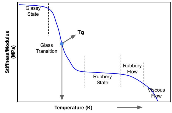
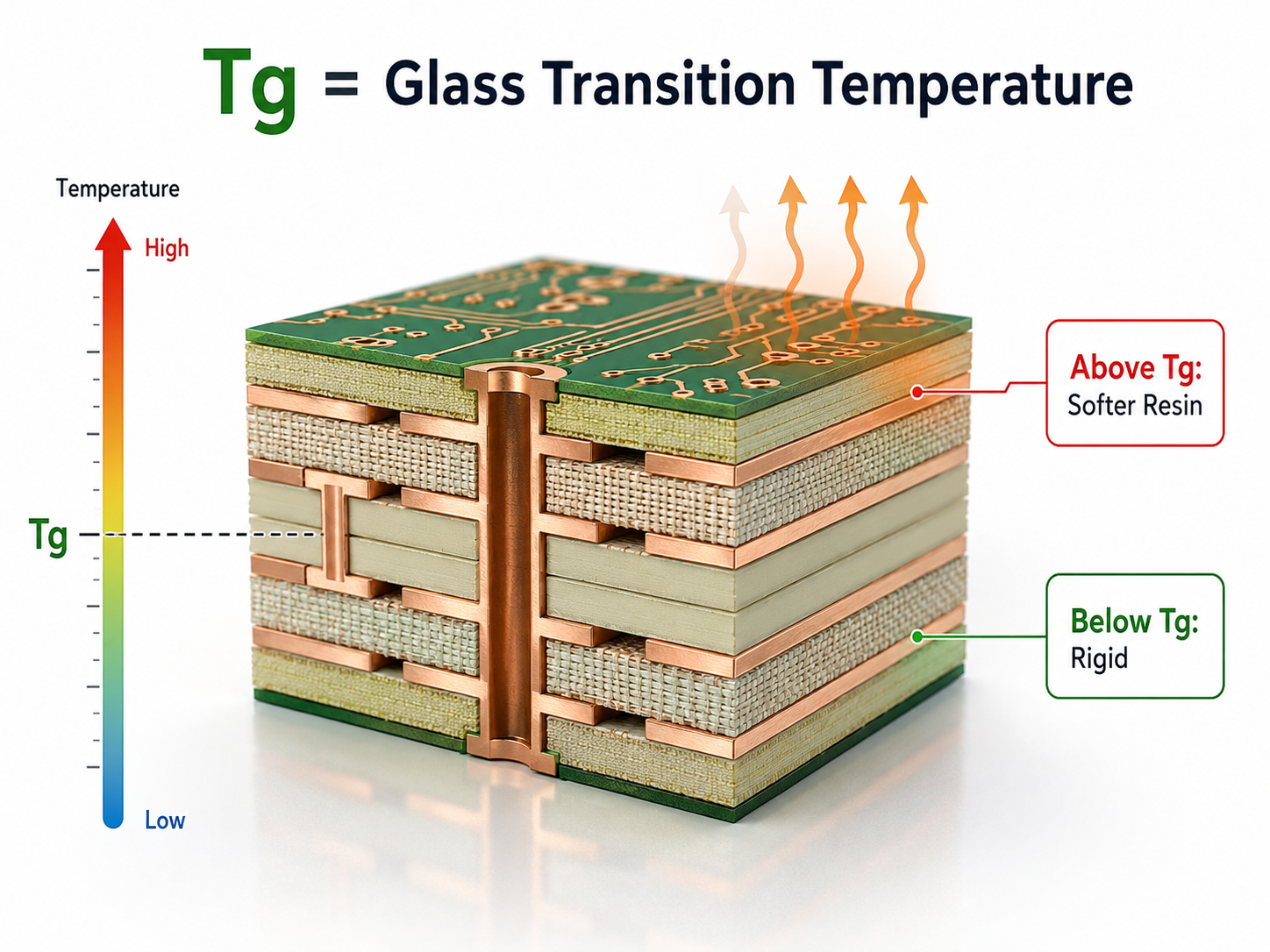
TG full form in PCB is glass transition temperature. In PCB material engineering, it is usually written as Tg, not TG, and it describes the temperature range where the resin system in a PCB laminate changes from a hard, glass-like condition to a softer, more flexible state.
For engineers and buyers, Tg is not just a material label. It affects dimensional stability, plated through-hole reliability, soldering performance, delamination risk, and long-term service life. When a PCB will face lead-free reflow, high operating temperature, dense multilayer construction, automotive electronics, power modules, or harsh environments, selecting the right Tg value becomes a practical reliability decision.
What Is the TG Full Form in PCB Materials?
The TG full form in PCB materials is glass transition temperature. It refers to the temperature region where the polymer resin inside the laminate begins to lose stiffness and becomes more rubber-like.
Most common FR4 PCB materials are made from woven glass fabric and epoxy resin. The glass fiber provides mechanical reinforcement, while the resin bonds the structure together. When the board temperature stays below Tg, the laminate remains relatively rigid and dimensionally stable. When the temperature approaches or exceeds Tg, the resin expands faster, softens, and becomes more vulnerable to mechanical and thermal stress.
This does not mean the PCB melts at Tg. A PCB laminate does not suddenly turn into liquid. Instead, its mechanical behavior changes. That is why Tg should be understood as a reliability threshold, not a simple maximum working temperature.
Why Does Tg Matter in PCB Design and Manufacturing?
Tg matters because it influences how well a PCB survives heat during assembly, operation, and environmental stress. A board with insufficient Tg may still pass a quick electrical test, but it can become less stable after repeated thermal exposure.
During PCB assembly, especially lead-free soldering, the board may experience peak reflow temperatures around 245–260°C depending on solder paste profile, component type, and thermal mass. Although the exposure time is short, the laminate must tolerate high thermal strain without delamination, excessive expansion, via cracking, or resin degradation.
In actual manufacturing, Tg becomes more important when the PCB has:
- Multiple reflow cycles
- Dense multilayer stack-up
- Small vias or high aspect ratio plated holes
- Heavy copper areas
- Large components with high thermal mass
- Long operating time near elevated temperature
- Automotive, industrial, power, LED, or communication applications
A proper Tg selection helps the PCB maintain shape, bonding strength, and electrical insulation after heat exposure. It also gives the fabricator a safer process window during lamination, drilling, plating, solder mask curing, and assembly.
How Does Glass Transition Temperature Work in a PCB Laminate?
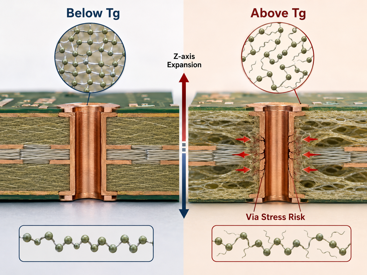
Glass transition temperature works through the resin system inside the laminate. Below Tg, resin molecules have limited movement, so the material remains stiff. Near and above Tg, molecular movement increases, and the material becomes more flexible.
This change affects several PCB behaviors at the same time. The Z-axis expansion usually increases, meaning the board becomes more likely to expand through its thickness. This is important because plated through holes and vias run through that same irection. When the laminate expands too much, copper barrels may stretch, fatigue, or crack.
Tg also affects warpage control. A laminate that softens too much during high-temperature processing may move unevenly, especially when copper distribution is unbalanced. This can cause assembly problems such as poor solder joint formation, BGA coplanarity issues, or connector misalignment.
In simple terms, Tg tells you when the board material starts to behave differently under heat. Good PCB design does not only ask, “What is the Tg value?” It also asks, “How will this material behave during real production and field use?”
What Are the Main Tg Ranges for PCB Materials?
PCB Tg ranges vary by laminate family, resin chemistry, and test method. Many engineers use Tg categories as a quick material selection guide, but the final decision should also consider Td, CTE, copper thickness, layer count, reflow profile, and reliability requirements.
| Material Category | Typical Tg Range | Common PCB Use | Relative Cost | Key Limitation |
|---|---|---|---|---|
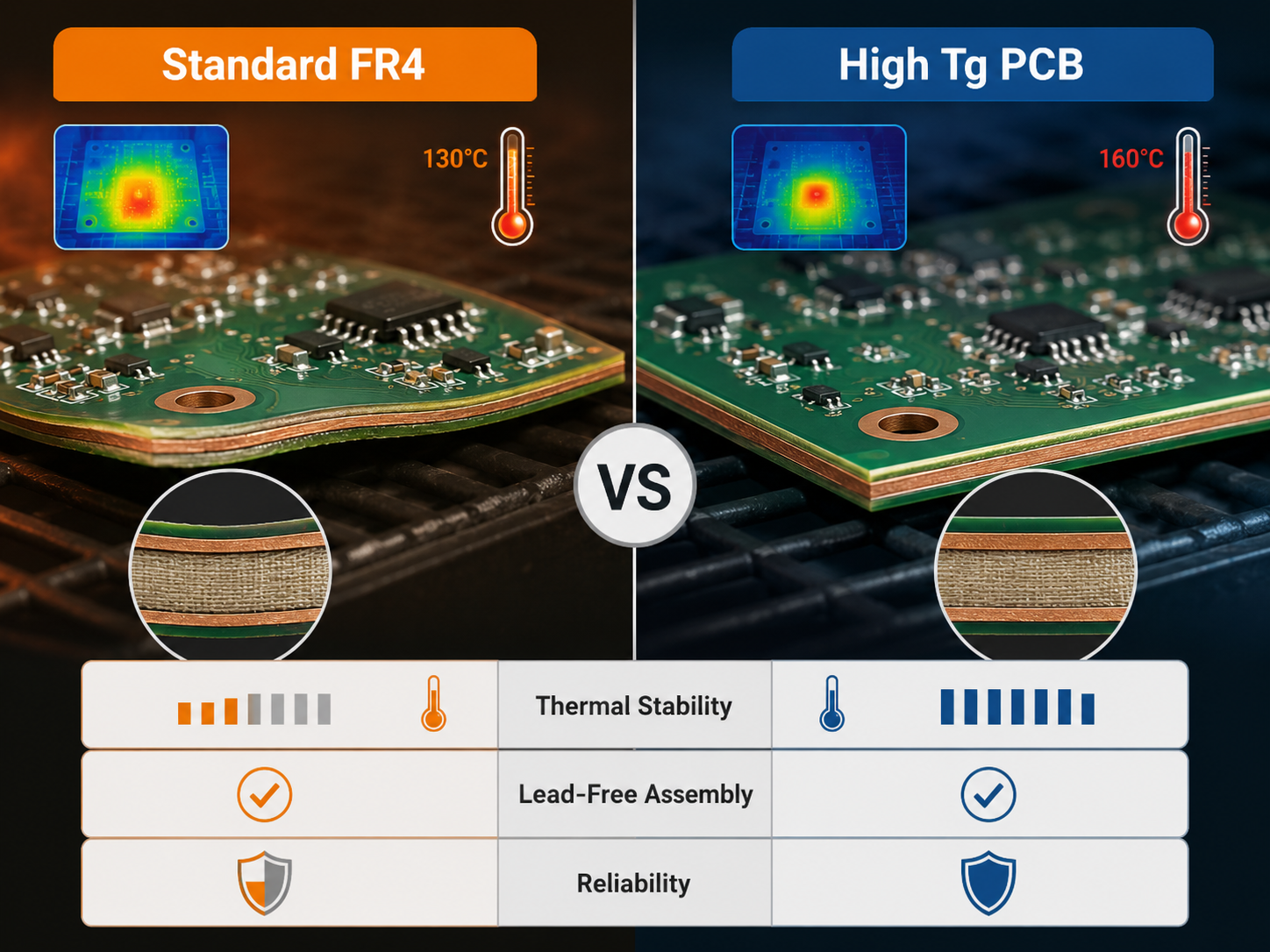
| Standard FR4 | About 130–150°C | Consumer electronics, simple industrial boards, low to medium thermal demand | Low | Less suitable for repeated high-temperature exposure |
| Mid Tg FR4 | About 150–170°C | General multilayer PCB, moderate assembly and reliability requirements | Medium | May not be enough for harsh thermal cycling |
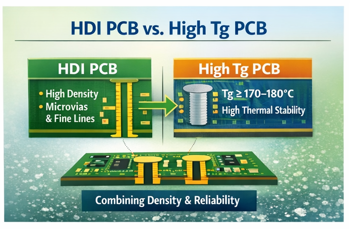
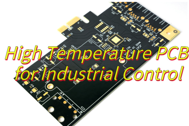
| High Tg FR4 | About 170–180°C+ | Automotive, industrial control, power electronics, dense multilayer boards | Medium to high | Higher material cost and more process control required |
| High-performance FR4 / lead-free laminate | Around 180–200°C+ depending on system | High-reliability multilayer PCB, multiple reflow cycles, higher thermal stress | High | Needs correct stack-up and lamination control |
| High-frequency or specialty laminate | Depends on material family | RF, microwave, high-speed digital, hybrid stack-ups | High | Tg alone cannot define RF or signal performance |
A higher Tg value is useful, but it is not the only target. For example, a board with high Tg but poor Z-axis CTE may still have via reliability concerns. A lower-loss material may be better for RF design even if its Tg comparison is not the main selection factor.
What Materials Are Used in High Tg PCB Laminates?
High Tg PCB laminates usually use improved epoxy resin systems, multifunctional resin systems, or specialty resin blends. The goal is to improve thermal stability, reduce excessive expansion, and support more demanding assembly conditions.
High Tg FR4
This is the most common option for projects that need better heat resistance while keeping standard PCB fabrication compatibility. It is widely used in industrial electronics, power control boards, automotive modules, and multilayer PCB designs.
Lead-free compatible FR4
Lead-free assembly often requires higher peak soldering temperatures than older tin-lead processes. Lead-free compatible laminates are designed to survive modern reflow profiles with better thermal endurance.
Halogen-free high Tg materials
These materials are selected when environmental compliance or specific customer requirements limit halogen content. They may be used in consumer electronics, industrial control, and export-oriented products.
High-speed and high-frequency laminates
These materials focus on dielectric stability, low loss, controlled impedance, and signal integrity. Tg is still relevant, but Dk, Df, copper roughness, moisture behavior, and stack-up design often become more important.
Polyimide materials
Polyimide laminates offer strong thermal endurance and are used in demanding applications such as aerospace, military electronics, and high-temperature environments. They are usually more expensive and require experienced fabrication control.
Tg, Td, CTE, and MOT: What Is the Difference?
Tg is important, but it should not be read alone. Several thermal parameters work together when evaluating PCB material reliability.
| Parameter | Full Name | What It Means | Why It Matters |
|---|---|---|---|
| Tg | Glass transition temperature | Resin changes from rigid to more flexible behavior | Helps estimate thermal stability and expansion behavior |
| Td | Decomposition temperature | Material begins chemical degradation at a defined weight loss level | Important for lead-free assembly and long-term heat exposure |
| CTE | Coefficient of thermal expansion | How much the material expands with temperature | Critical for via reliability, warpage, and thermal cycling |
| MOT | Maximum operating temperature | Long-term operating temperature rating under defined conditions | Useful for application-level safety and service life |
| T260 / T288 | Time to delamination at 260°C / 288°C | How long material resists delamination at high temperature | Relevant for soldering and thermal stress screening |
A common mistake is choosing a PCB laminate only by Tg. In practice, a reliable board needs balanced thermal properties. For example, a high Tg material with low Z-axis expansion can be better than a material that only looks good on a datasheet headline. For multilayer boards, via reliability is often more closely related to thermal expansion and copper plating quality than to Tg alone.
Standard FR4 vs High Tg PCB: Which One Should You Choose?
Standard FR4 is suitable for many normal electronics. High Tg PCB is a better choice when the design faces higher heat, repeated reflow, dense multilayer construction, or long-term reliability requirements.
| Project Condition | Standard FR4 May Be Enough | High Tg PCB Is Recommended |
|---|---|---|
| Operating temperature | Low to moderate | Elevated or near thermal limit |
| Layer count | 1–4 layers, simple stack-up | 6 layers or above, dense routing |
| Assembly process | Single reflow, moderate thermal load | Multiple reflow cycles or high thermal mass |
| Copper design | Standard copper thickness | Heavy copper, large copper planes, power circuits |
| Via structure | Simple through holes | High aspect ratio vias, dense via arrays, BGA fanout |
| Product field | Consumer or basic commercial use | Automotive, industrial, power, LED, telecom, medical equipment |
| Reliability demand | Normal service environment | Thermal cycling, vibration, humidity, long service life |
If the board only works in a mild environment, high Tg material may not bring enough benefit to justify the added cost. If the board has a dense BGA, power section, high layer count, or harsh operating condition, high Tg material can reduce production risk and improve long-term stability.
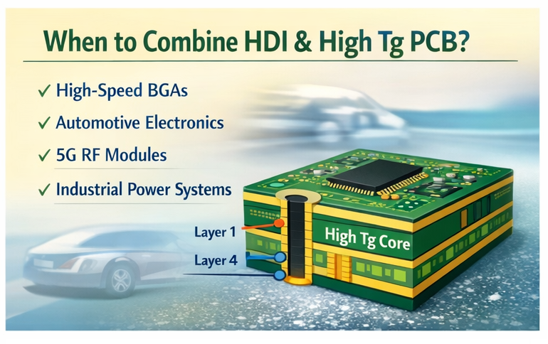
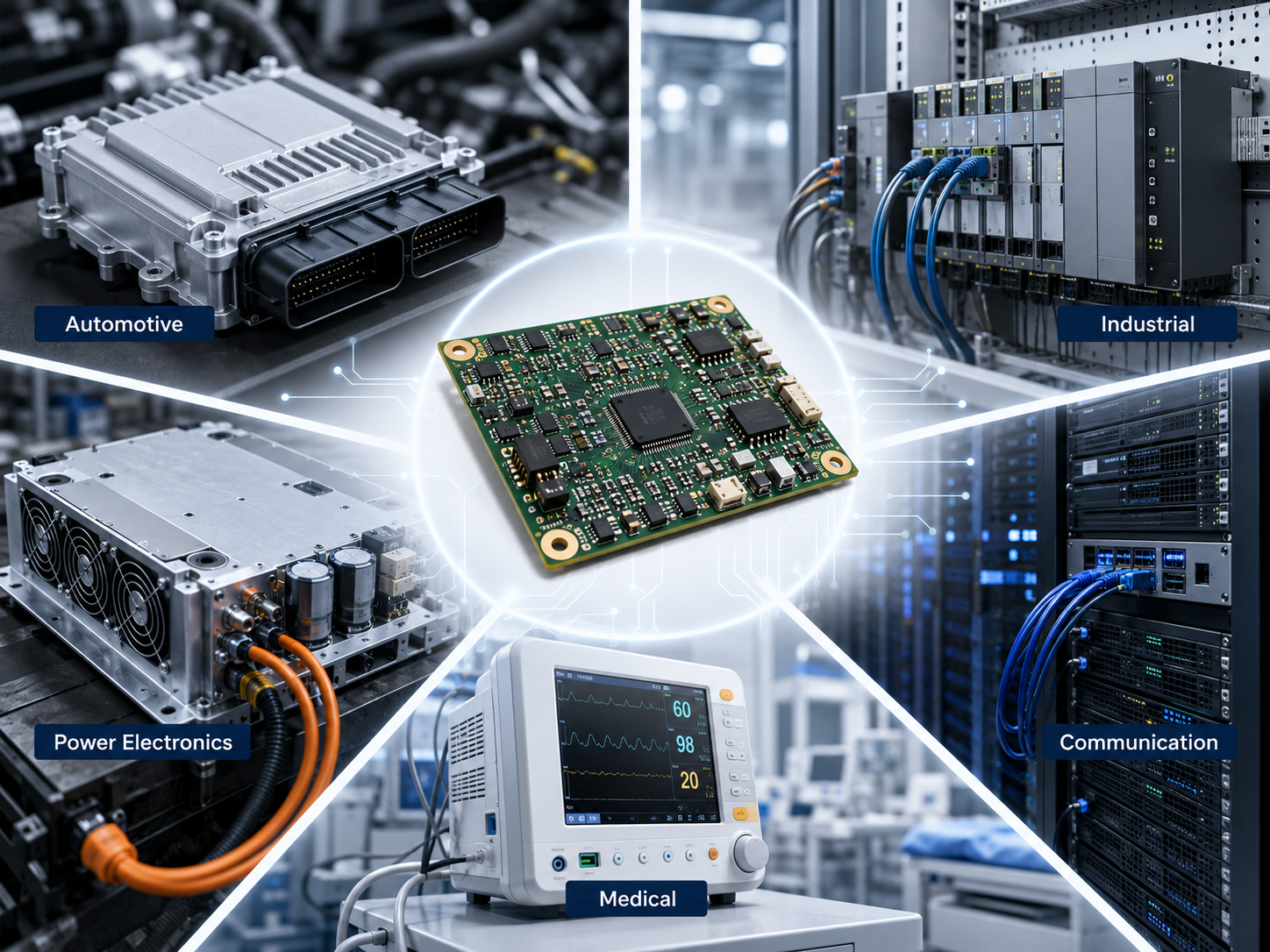
Where Are High Tg PCBs Used?
High Tg PCBs are used where heat, density, and reliability meet. They are common in electronics that must operate for long periods without material instability.
Automotive electronics
Engine control units, battery management systems, lighting modules, charging systems, and sensor control boards may face heat, vibration, and thermal cycling. High Tg materials help improve stability during both assembly and field use.
Industrial control systems
Motor drives, PLC modules, power controllers, and automation equipment often work near heat sources or inside enclosed cabinets. High Tg PCB materials support better thermal endurance.
Power electronics
Power supplies, inverters, converters, and high-current control boards may combine heavy copper, large pads, and repeated thermal load. High Tg selection can support better lamination stability and via reliability.
LED lighting and thermal products
High-power LED applications need careful thermal design. In some cases, metal core PCB, ceramic PCB, or copper base PCB may be more suitable than high Tg FR4. Still, high Tg FR4 can be useful for driver boards and control circuits.
Communication and high-speed electronics
Routers, base stations, servers, and high-speed modules need stable dielectric and mechanical performance. Tg is one part of the material decision, along with Dk, Df, impedance control, and copper roughness.
Medical and aerospace-related electronics
For regulated or mission-critical electronics, material consistency and traceability matter. High Tg laminates may be selected when the product requires higher process reliability and long-term environmental stability.
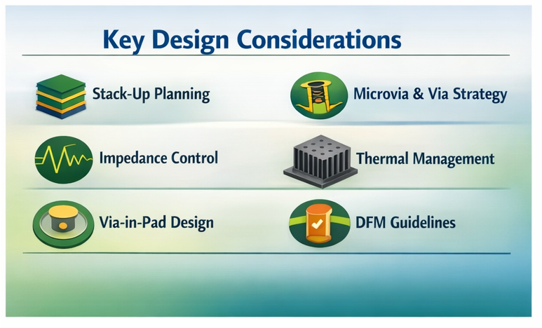
What Design Rules Help High Tg PCBs Stay Reliable?
High Tg material improves the process window, but design still decides much of the final reliability. A poorly balanced stack-up can create stress even when the material is good.
For high Tg PCB design, engineers should review these points before fabrication:
- Keep the stack-up symmetrical to reduce warpage.
- Balance copper distribution between layers where possible.
- Avoid extreme copper imbalance around large planes and open areas.
- Confirm dielectric thickness for impedance and lamination stability.
- Use proper annular ring and drill-to-copper clearance.
- Avoid unnecessary high via aspect ratios.
- Add thermal relief only where solderability requires it.
- Match material Tg, Td, and CTE with the assembly profile.
- Define controlled impedance requirements clearly.
- Specify IPC class and acceptance criteria when reliability is critical.
BGA areas need special attention. The fabricator should review pad size, solder mask defined or non-solder mask defined pads, via-in-pad filling, microvia structure, and flatness. When a board has both high-density routing and high thermal exposure, early DFM review can prevent expensive rework later.
What Manufacturing Controls Matter for High Tg PCB?
High Tg PCB manufacturing requires good control over lamination, drilling, plating, solder mask curing, surface finish, and final inspection. The material is stronger than standard FR4 in thermal behavior, but it still needs correct processing.
Material verification
The laminate and prepreg should match the customer’s required Tg grade, IPC slash sheet, material brand, or approved equivalent. Substitution should not happen without approval when reliability is important.
Lamination profile control
High Tg materials often need proper temperature, pressure, vacuum, and curing time. Poor lamination can lead to voids, weak bonding, or hidden delamination risk.
Drilling and desmear control
High Tg resin systems may behave differently during drilling and hole preparation. Drill quality affects hole wall smoothness, plating adhesion, and through-hole reliability.
Copper plating quality
Vias and plated through holes must have sufficient copper thickness and uniform coverage. Thermal cycling stress often concentrates at copper barrels.
Solder mask and surface finish compatibility
The solder mask and surface finish should match the assembly process. ENIG, immersion silver, immersion tin, OSP, and HASL each have different handling and solderability considerations.
Inspection and testing
AOI, electrical testing, microsection inspection, solderability checks, thermal stress testing, and impedance testing may be required depending on the product class.
A strong factory does not only ask what Tg you want. It checks whether the selected material, stack-up, copper design, drilling structure, and assembly process are aligned.
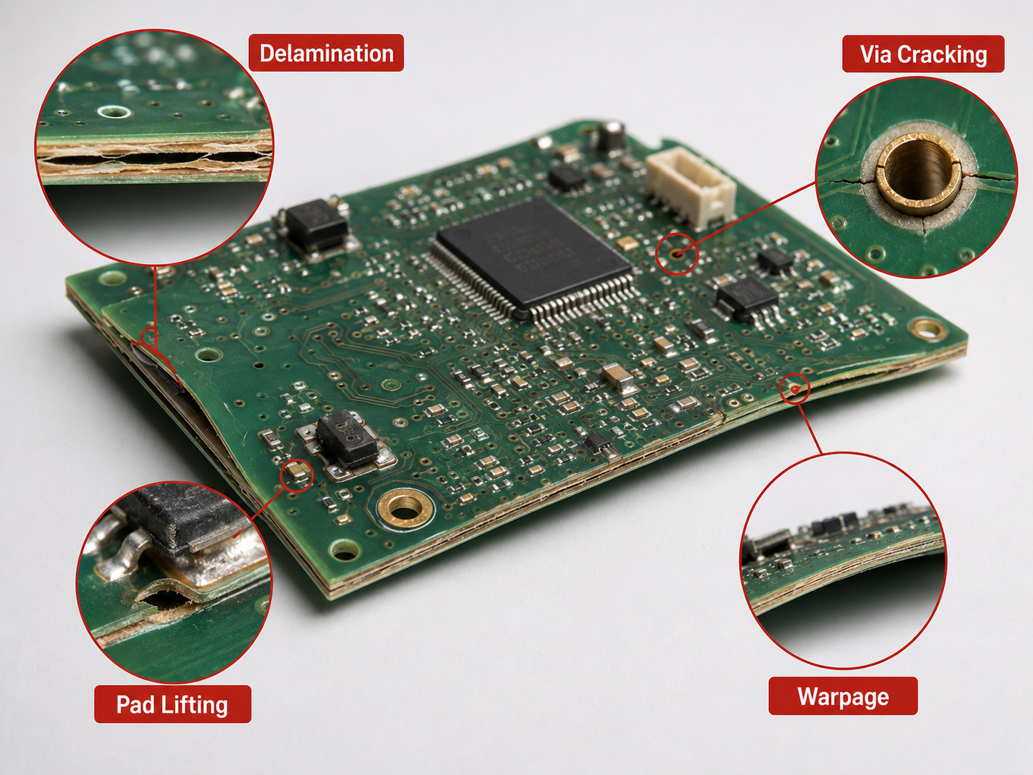
What Failures Can Happen When Tg Is Chosen Poorly?
When Tg is too low for the real operating or assembly condition, the PCB may show several reliability issues. Some failures appear during production. Others appear after months of use.
| Failure Mode | Possible Cause | Typical Sign | Practical Prevention |
|---|---|---|---|
| Delamination | Resin expansion, weak bonding, excessive heat exposure | Blistering, layer separation, popcorn-like damage | Use suitable Tg/Td material and controlled lamination |
| Via barrel cracking | High Z-axis expansion and thermal cycling | Intermittent open circuit, failed continuity test | Improve material CTE, plating thickness, and via design |
| Pad lifting | Resin softening and poor copper adhesion | Pads detach during rework or soldering | Select better laminate and control soldering temperature |
| Warpage | Unbalanced copper, high heat, stack-up asymmetry | BGA solder joint issues, assembly flatness problems | Balance stack-up and copper distribution |
| CAF risk | Moisture, voltage bias, poor material or process control | Leakage path between conductors | Use CAF-resistant material and proper spacing or cleanliness control |
| Solder joint fatigue | Board movement under thermal cycling | Cracked solder joints near large components | Improve material stability and assembly design |
Failure analysis should not stop at “material problem.” A Tg-related failure may also involve stack-up design, copper imbalance, moisture absorption, reflow profile, drill quality, plating control, or poor storage. The best solution is a combined review of design files, material certificates, production records, and assembly conditions.
How Much Does a High Tg PCB Cost and How Should Buyers Specify It?
High Tg PCB usually costs more than standard FR4 because the laminate is more expensive and the process may require tighter control. The cost increase depends on material grade, board size, layer count, copper thickness, surface finish, impedance control, tolerance, test requirements, and order quantity.
Buyers should not request only “high Tg” without details. The term can be interpreted differently by different suppliers. A clear RFQ should include:
- Required Tg value or approved material model
- IPC-4101 slash sheet if specified by the project
- Layer count and stack-up
- Board thickness and tolerance
- Copper thickness for inner and outer layers
- Minimum trace width and spacing
- Minimum hole size and via aspect ratio
- Surface finish
- Solder mask color and legend requirements
- Controlled impedance requirements
- IPC class requirement
- Assembly process, if PCBA is included
- Expected operating environment
- Quantity, delivery schedule, and testing requirements
For cost control, buyers can ask the supplier to suggest an equivalent material, but the approval should be based on datasheet comparison and project risk. For automotive, medical, aerospace-related, or long-life industrial products, material substitution should be handled carefully.
How to Choose a High Tg PCB Supplier?
A reliable high Tg PCB supplier should understand both material selection and production control. The supplier should be able to review the design before quoting, explain material options, and identify risks that may affect yield or long-term reliability.
When selecting a supplier, check whether they can support:
- High Tg FR4 and lead-free compatible materials
- Multilayer PCB stack-up engineering
- Controlled impedance design and testing
- Heavy copper and thermal design review
- Via reliability control and microsection inspection
- Material traceability
- AOI and electrical testing
- PCBA support if assembly is required
- Engineering feedback before mass production
- Stable delivery for prototypes and batch orders
For overseas buyers sourcing from China, the key is not to find the lowest material quote. The stronger approach is to choose a source factory that can review manufacturability, confirm material availability, provide clear communication, and support both prototype and mass production. This reduces the risk of redesign, rework, delayed delivery, and hidden quality issues.
Best Technology supports custom PCB and PCBA manufacturing for FR4 PCB, high Tg PCB, multilayer PCB, heavy copper PCB, metal core PCB, ceramic PCB, flexible PCB, rigid-flex PCB, high-frequency PCB, and turnkey assembly projects. For projects with thermal stress or long-term reliability requirements, our engineering team can review your Gerber files, stack-up, copper thickness, material needs, and assembly conditions before quotation.
Frequently Asked Questions
Q1: What is the TG full form in PCB?
A1: TG full form in PCB is glass transition temperature, commonly written as Tg. It describes the temperature range where the resin in a PCB laminate changes from a hard, glass-like state to a softer and more flexible state. It is important because this change affects expansion, rigidity, warpage, via reliability, and heat resistance during soldering and product operation.
Q2: Is Tg the same as melting temperature?
A2: No. Tg is not the melting temperature. PCB laminate resin does not simply melt at Tg. Instead, it changes mechanical behavior and becomes less rigid. The board may still remain solid, but its expansion and stress behavior can change noticeably. This is why Tg is used as a reliability indicator rather than a melting point.
Q3: What is considered a high Tg PCB?
A3: In many PCB projects, high Tg PCB usually refers to laminates with Tg around 170°C or higher, although some suppliers classify high Tg above 180°C depending on the material system and test method. The safest way is to specify the exact Tg value, material model, or IPC material requirement instead of using only the phrase “high Tg.”
Q4: Do all PCB projects need high Tg material?
A4: No. Standard FR4 is suitable for many consumer, commercial, and low-thermal-stress applications. High Tg material becomes more valuable when the PCB has high operating temperature, multiple reflow cycles, dense multilayer structure, heavy copper, high via density, or stricter reliability requirements. The best choice depends on product environment, not only material grade.
Q5: Why is high Tg PCB more expensive?
A5: High Tg PCB is more expensive mainly because the laminate costs more and fabrication may need tighter process control. Cost can also increase with layer count, copper thickness, controlled impedance, surface finish, material brand, testing requirements, and delivery urgency. However, in high-reliability products, the added material cost may reduce failure risk and rework cost.
Call to Action
TG full form in PCB is glass transition temperature, and its real value is in helping engineers and buyers judge thermal reliability. A suitable Tg value can support better dimensional stability, stronger via reliability, safer lead-free assembly, and longer product life. Still, Tg should always be evaluated together with Td, CTE, copper design, stack-up, assembly profile, and operating environment.
For selection, standard FR4 is practical for mild applications, while high Tg PCB is better for dense multilayer boards, power electronics, automotive modules, industrial control systems, and products exposed to repeated heat. For procurement, the most important step is to define material requirements clearly and choose a supplier that can review manufacturability before production.
If you need high Tg PCB, FR4 PCB, multilayer PCB, heavy copper PCB, metal core PCB, ceramic PCB, rigid-flex PCB, or turnkey PCB assembly, you can send your Gerber files, stack-up, material requirements, copper thickness, surface finish, quantity, and application details to our engineering team at sales@bestpcbs.com for technical review and quotation.