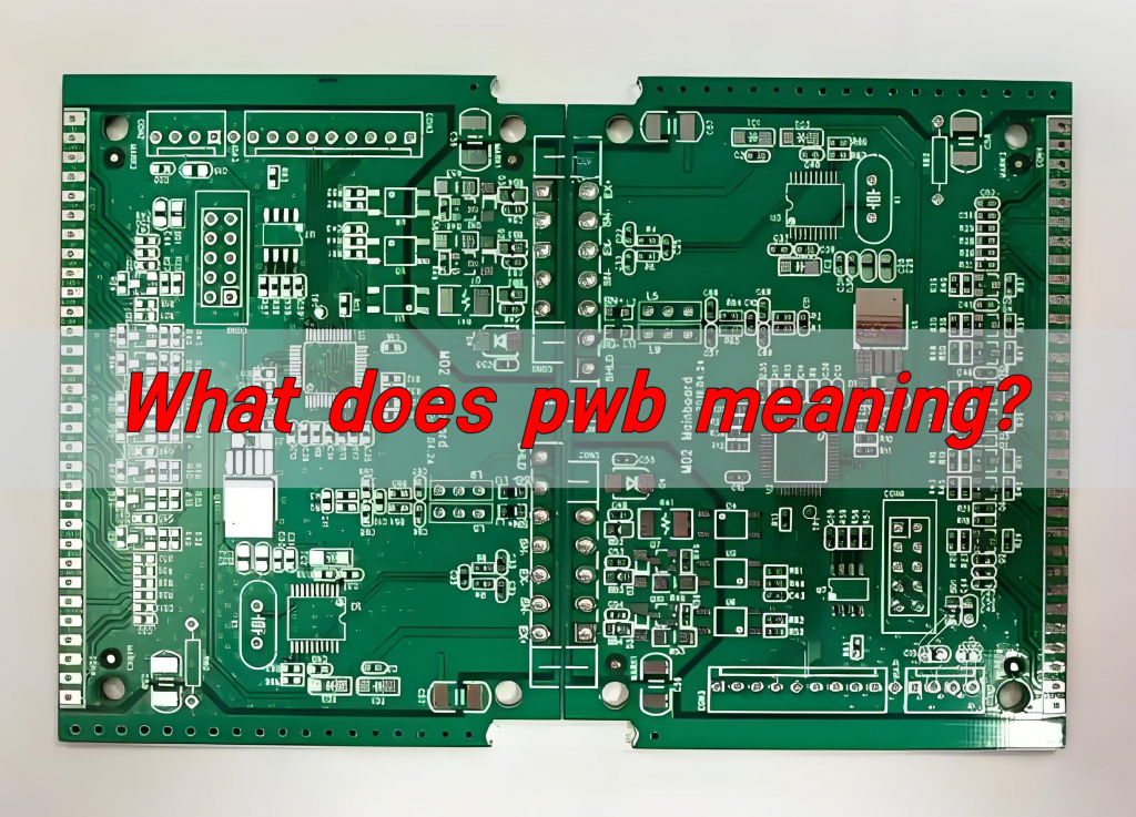
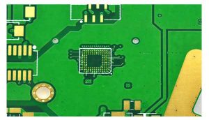
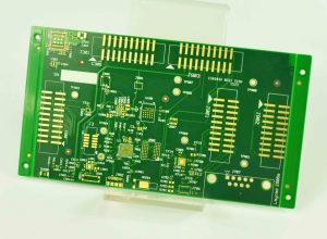
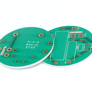
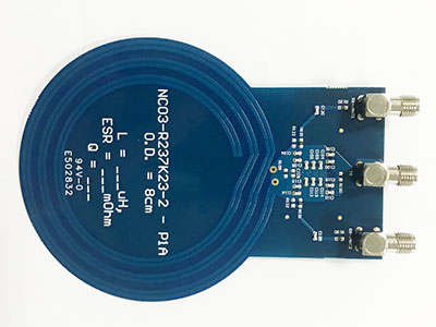
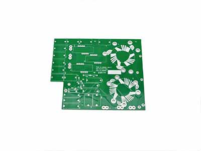
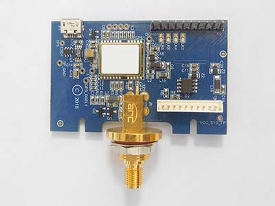
What does pwb meaning? PWB is the abbreviation of Printed Wiring Board. It originated from the need for electronic component connection carriers in the early development of electronic technology. Early electronic devices were relatively simple, and the electrical connection between electronic components was mainly achieved by printing metal circuits on insulating substrates. These circuits are like precise “roads” that guide the current to be transmitted between components, so that electronic devices can work properly.
What does the term PWB mean?
PWB refers to Printed Wiring Board, which is a carrier that uses conductors on an insulating substrate to form interconnected circuits between devices. PWB is an important component of electronic equipment and is used to achieve electrical connections between electronic components.
In the field of electronic manufacturing, PCB (Printed Circuit Board) and PWB (Printed Wiring Board) have a close connection and a specific historical evolution. Today, in most parts of the world, PCB and PWB actually refer to the same item, but the term PCB is more commonly used. They are all circuit boards made by laminating one or more layers of copper foil onto a non-conductive plastic panel. Their main function is to provide support and connection for components with conductive tracks.
However, in some countries such as Japan, since PCB happens to be the name of a common poison, polychlorinated biphenyls, in order to avoid confusion, people prefer to use PWB to refer to this circuit board.
Looking back at the development of the electronics manufacturing industry, PWB has been used in the early days of the industry. At that time, the circuit connection method was relatively simple, mainly in the form of point-to-point connection. With the continuous advancement of technology, wires began to cross from one side of the board to the other, and even from one layer to another. The design of circuit boards is no longer limited to simple point-to-point connections, but has been given specific functions to meet the needs of increasingly complex electronic equipment.
In this process, PCB gradually emerged and eventually replaced the traditional point-to-point wiring board. In 1999, the IPC committee made a decision to clarify the unified use of the term PCB in the future, thus establishing the dominant position of PCB in industry specifications.
In the context of modern electronic manufacturing in most parts of the world, PWB can be regarded as the old name of PCB, while PCB has become a common and standard name for bare circuit boards without components. The unification of this term helps the global electronic manufacturing industry to standardize and normalize in terms of technical exchanges, production and manufacturing, and market circulation.
What is a PCB?
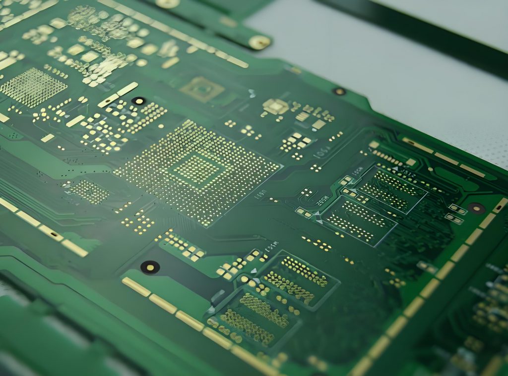
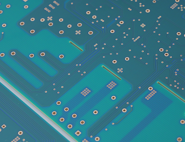
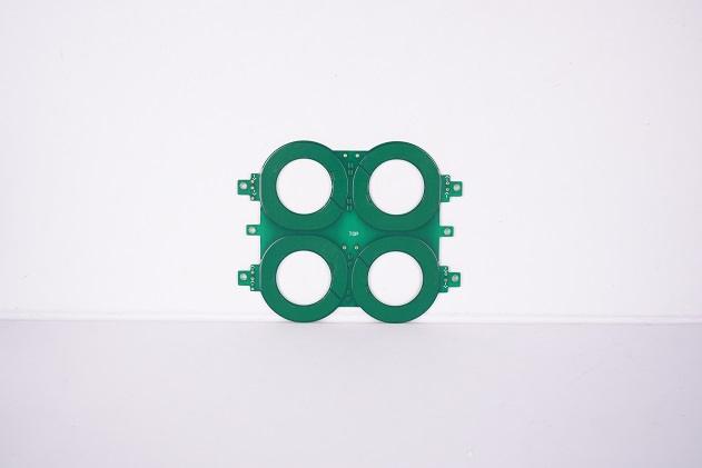
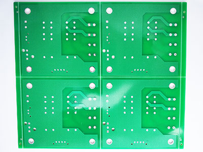
PCB, or printed circuit board, is an indispensable and important component in electronic equipment, used to achieve electrical connections between electronic components. It forms electrical connections between electronic components and supports and fixes components by laying conductive copper foil patterned on insulating materials.
PCB mainly consists of the following parts:
- Substrate: Usually made of glass fiber or epoxy resin, providing mechanical support and insulation functions.
- Conductive layer: Made of copper foil, responsible for transmitting current and signals.
- Solder mask: Protects the copper foil of the circuit board from oxidation and prevents short circuits.
- Character layer: Marks the position of components on the circuit board for easy assembly and maintenance.
According to the number of conductive layers, PCBs can be divided into the following categories:
- Single-sided board: Only one side is a conductive layer, suitable for low-complexity circuits, such as simple home appliances or electronic toys.
- Double-sided board: Both sides have conductive layers, suitable for more complex circuits, such as computers, automotive electronics, etc.
- Multilayer board: There are four or more conductive layers, connected by internal wires, suitable for highly integrated circuits, such as communication equipment, high-end servers, etc.
What is the difference between PWB and PCB?
PWB (Printed Wiring Board), PCB (Printed Circuit Board), the difference between them is mainly reflected in the following aspects:
1. Origin of the name and emphasis on the meaning
- PWB: In the early days, it mainly emphasized the printing of circuits, focusing on forming conductive circuits on the substrate through printing technology to achieve electrical connections between electronic components, and focusing more on the layout and construction of circuits.
- PCB: It emphasizes the concept of circuits more, not only including conductive circuits, but also covering various electrical characteristics, signal transmission paths, and circuit function realization in circuit design. It is a more comprehensive term, involving the entire scope from circuit principles to actual physical layout.
2. Historical development context
- PWB: It was widely used in the early stages of the development of the electronic manufacturing industry. At that time, electronic equipment was relatively simple, and the circuit was mainly a relatively simple point-to-point connection method. PWB could meet the basic line connection needs and provided a basic support platform for the assembly of early electronic products.
- PCB: With the rapid development of electronic technology, the functions of electronic products have become more and more complex. PCB has gradually developed. It is not just a simple line connection, but also incorporates more circuit design concepts and technologies, thus gradually occupying a dominant position in the industry and largely replacing the early PWB.
3. Application scope and industry habits
- PWB: Although it is no longer dominant in modern electronic manufacturing, the term PWB may still be used in some specific fields or traditional electronic equipment manufacturing, especially in some cost-sensitive, relatively simple circuit functions and low requirements for the application of new technologies. Some companies or engineers may continue to use the name PWB.
- PCB: Currently widely used in the manufacture of various electronic equipment worldwide, PCB has become an indispensable basic component in the electronic manufacturing industry and a common standard term in the industry, which helps to improve the communication efficiency and standardization of the industry.
4. Technical standards and specifications
- PWB: Due to its early application background and relatively simple technical characteristics, the relevant technical standards and specifications are relatively basic and simple, mainly focusing on basic circuit printing quality, line width and line spacing, and conduction performance. With the gradual reduction of PWB usage scenarios, the update and development of its technical standards are also relatively slow.
- PCB: With the continuous advancement of technology and the continuous expansion of application fields, the technical standards and specifications of PCB have become extremely rich and strict. These standards and specifications are formulated and updated by international organizations (such as IPC – International Electronics Industry Connecting Association) and industry associations in various countries to ensure that the quality and performance of PCB can meet the needs of electronic products in different industries and different application scenarios.
Although there may be no essential difference between modern PWB and PCB in actual physical products, they have the above-mentioned differences and characteristics from multiple dimensions such as the origin of the term, historical development, scope of application, industry habits, and technical standards. In today’s electronic manufacturing industry, PCB is a more commonly used and widely recognized term, representing advanced electronic circuit manufacturing technology and complex circuit design concepts.
What are the common circuit board terms?
PB is the standardized name for bare board, which stands for printed board; PCBA is the abbreviation for printed circuit board assembly. When the PCB is assembled, it is called PCBA or PCB assembly. PCBA has been the term for all assembled circuit boards since the change in 1999. From users to technical committees, PCBA is also the preferred term for assembled boards.
PWA is the abbreviation for printed wiring assembly. It is an old term for PCB assembly or PCBA.
CCA is the abbreviation for circuit card assembly. CCA is the same as PCBA, but CCA is a less used term.
PCA is the abbreviation for printed circuit assembly. PCA is also the same as PCBA and is not common now.
From this we can conclude that PWB, PCB, circuit board are the same thing, referring to bare printed circuit boards; while PCA, CCA, PWA, PCBA are the same thing, referring to assembled circuit boards. Among them, PCB and PCBA are the two most widely used terms.
In short, although PWB, as a printed circuit board, has some subtle differences in terminology from PCB, in essence they are both indispensable basic components in electronic devices. They have witnessed the development of electronic technology together and will continue to play an important role in the future technological wave.


