PCB manufacturing PCB manufacturing
Home > Blog

pcba assembly

5-in-1 Antenna PCB Layout, Fabrication, and PCBA Assembly
Wednesday, May 27th, 2026

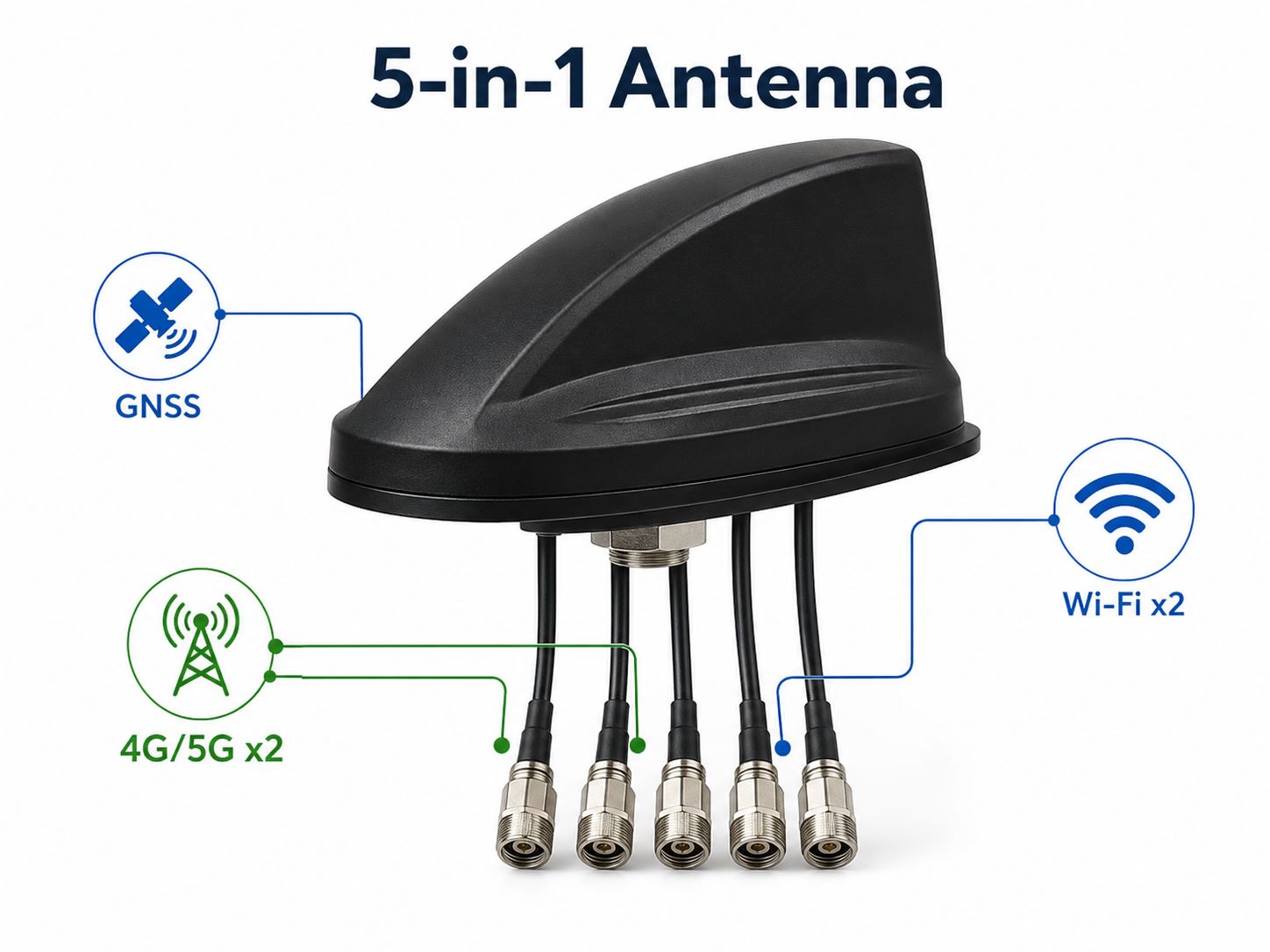
A 5-in-1 antenna usually combines GNSS, 4G/5G cellular, and Wi-Fi signal paths in one antenna unit. It is common in IoT gateways, vehicle trackers, industrial routers, smart transportation devices, and outdoor wireless terminals.

This guide focuses on the checks a PCB/PCBA manufacturer can realistically support before fabrication, assembly, and shipment. In many 5-in-1 antenna PCB and PCBA projects, the antenna is connected through RF interfaces such as SMA connector PCB, SMB PCB, UFL Connector PCB, BNC PCB, or MMCX PCB. If your wireless device requires RF connector assembly, controlled impedance PCB fabrication, or PCBA production review, you can send your Gerber files, BOM, and assembly requirements to sales@bestpcbs.com.

5-in-1 Antenna

What Is a 5-in-1 Antenna?

A 5-in-1 antenna is an integrated antenna solution with five wireless signal paths. A common structure includes:

  • 1x GNSS antenna
  • 2x 4G/5G cellular MIMO antennas
  • 2x Wi-Fi MIMO antennas

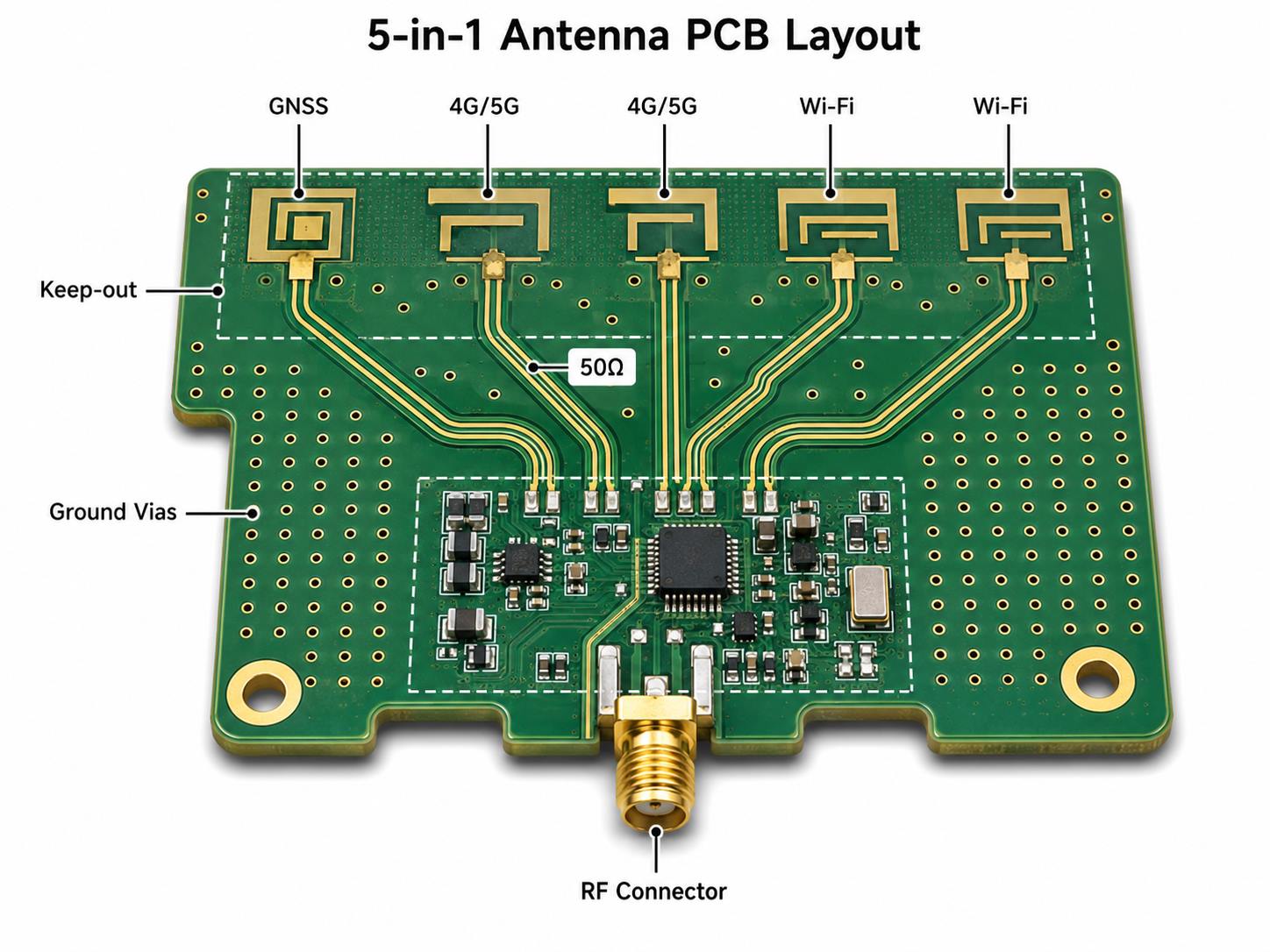
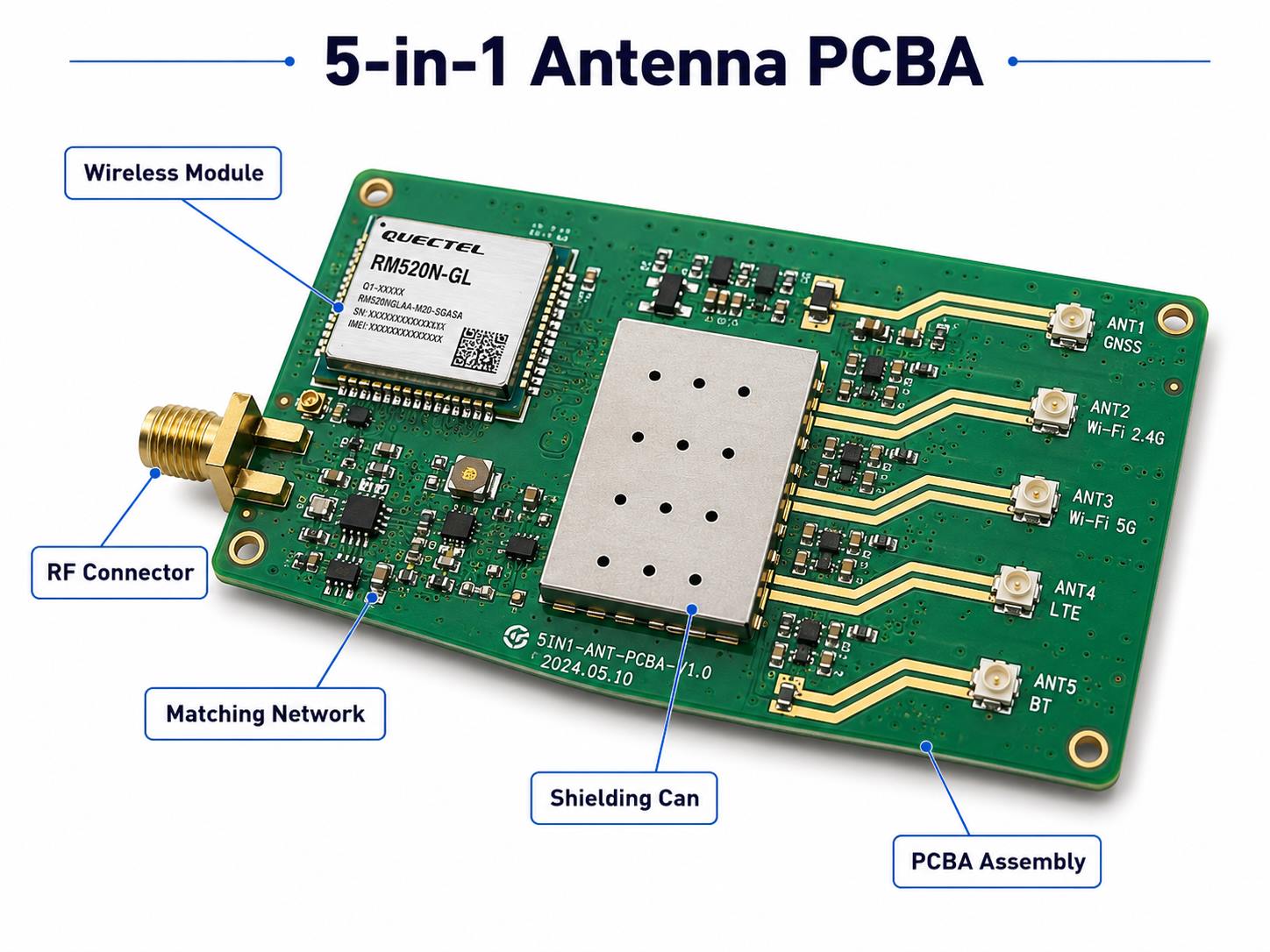
In a real device, the antenna connects to the PCB assembly through RF connectors, coaxial cables, wireless modules, matching circuits, ESD protection parts, and controlled impedance traces.

A PCB/PCBA manufacturer does not replace the antenna engineer. Its value is to check whether the PCB files, stackup, impedance notes, RF connector footprint, BOM, assembly drawing, and test requirements are ready for production.

5-in-1 Antenna

Common PCB and PCBA Risks in 5-in-1 Antenna Projects

Problem Found LaterCommon Manufacturing CauseWhat Should Be Checked Early
Weak GNSS receptionPoor RF path control or unclear layout notesGNSS path, impedance note, connector area, module guide
Unstable 4G/5G connectionImpedance mismatch or connector issue50Ω trace, stackup, RF connector footprint
Poor Wi-Fi performanceTrace discontinuity or cable assembly issueWi-Fi RF path, connector placement, coaxial cable route
Prototype works, batch variesStackup changed or impedance not controlledStackup drawing, impedance coupon, fabrication tolerance
RF connector becomes looseWrong footprint or weak pad designConnector datasheet, pad size, solder mask opening
RF matching issueWrong value or misplaced small componentsBOM, placement file, first article inspection
Shielding issuePoor soldering or incomplete groundingShielding can footprint, solderability, ground pads

These problems are expensive because they often appear after SMT assembly or final testing. Early manufacturing review is much cheaper than redesign, rework, or repeated debugging.

What Should Be Checked Before PCB Fabrication?

Before PCB fabrication, the main task is to confirm whether the board data can support stable RF-related production.

1. Stackup

Stackup affects impedance, trace width, return path, and signal loss. For antenna-related products, stackup should be confirmed before production.

Check:

  • Layer count
  • Dielectric thickness
  • Copper thickness
  • RF reference layer
  • Solder mask condition
  • Material availability
  • Impedance tolerance

2. 50Ω RF Trace Requirement

Most GNSS, cellular, and Wi-Fi feed lines use 50Ω controlled impedance. This requirement should be clearly marked in the fabrication notes.

Customers should provide:

  • Target impedance
  • Controlled impedance layer
  • Trace width and spacing
  • Stackup drawing
  • Impedance tolerance
  • Test coupon requirement

Without clear impedance notes, the board may be treated as a normal PCB instead of an RF-controlled board.

3. RF Connector Footprint

RF connector problems are common in antenna-related PCBA projects. SMA, U.FL, IPEX, MMCX, and board-to-board RF connectors all have specific footprint requirements.

Check:

  • Pad size
  • Ground pad connection
  • Solder mask opening
  • Connector orientation
  • Edge clearance
  • Cable direction
  • Rework space

A small footprint error can cause soldering defects, weak contact, or unstable field performance.

RF Connector Area and Assembly Clearance

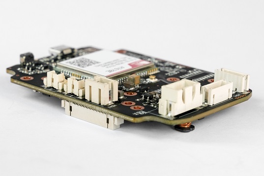
The RF connector area should be reviewed before PCB fabrication and PCBA assembly. For a 5-in-1 antenna product, connector placement and nearby PCB details can affect soldering quality, cable installation, inspection, rework access, and production consistency.

A PCB/PCBA manufacturer can help check whether the connector footprint, solder mask opening, ground pads, board edge clearance, and cable direction match the assembly requirement. If the customer provides a wireless module layout guide or antenna reference design, the manufacturer can also review whether the board files follow the key manufacturing notes.

Check before production:

  • RF connector footprint against the datasheet
  • Pad size and solder mask opening
  • Ground pad connection around the connector
  • Board edge clearance
  • Cable plugging direction
  • Space for manual inspection and rework
  • Coaxial cable bend radius
  • Shielding can footprint and solderability, if used
  • Keep-out notes provided by the module or antenna supplier

This review does not replace antenna tuning, OTA testing, or RF chamber testing. Its purpose is to reduce assembly risk, connector failure, soldering defects, and avoidable layout-to-production problems.

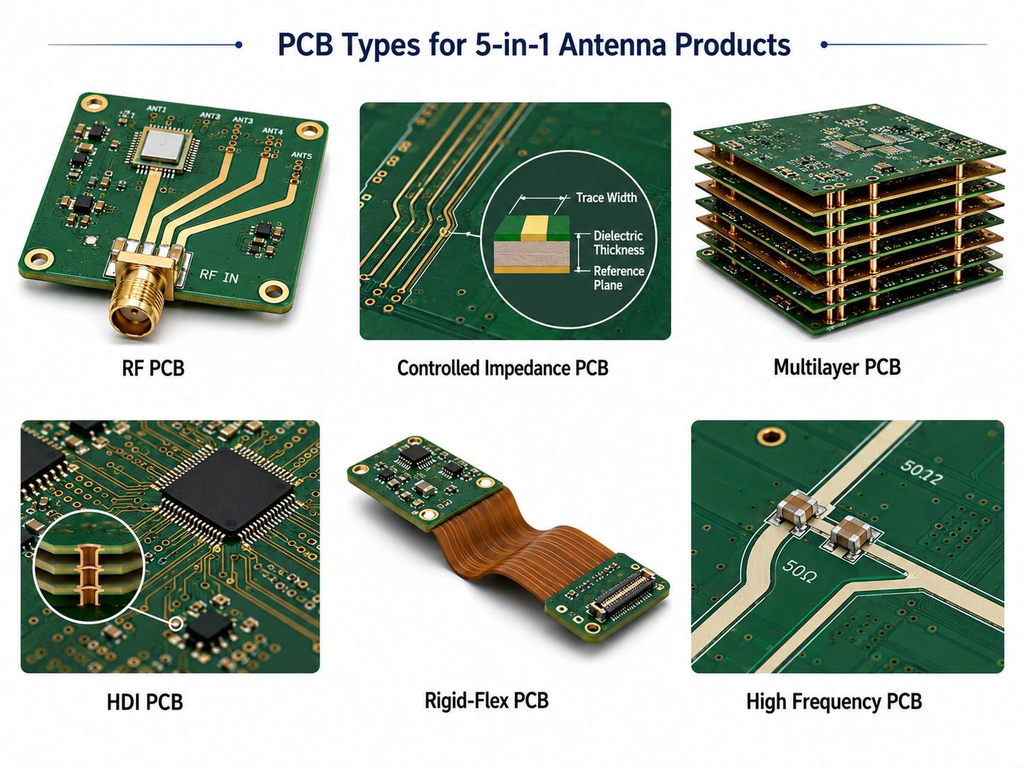
What Types of PCBs Are Used in 5-in-1 Antenna Products?

Different products need different PCB structures. The PCB type should match the RF requirement, space limit, assembly method, and working environment.

PCB TypeTypical UseManufacturing Value
RF PCBAntenna feed lines, wireless modulesBetter RF trace and impedance control
High Frequency PCBHigher-frequency or lower-loss RF pathsMore stable signal transmission
Controlled Impedance PCBGNSS, cellular, Wi-Fi RF tracesKeeps 50Ω signal paths consistent
Multilayer PCBGateways, routers, tracking devicesBetter grounding, routing, and power distribution
HDI PCBCompact wireless devicesSupports fine-pitch modules and dense routing
Rigid PCBIndustrial and outdoor devicesStable structure for connectors and modules
Flexible PCBSpace-limited internal connectionsFits compact mechanical structures
Rigid-Flex PCBMulti-section compact devicesReduces connectors and improves reliability
High-TG PCBAutomotive, outdoor, industrial productsBetter thermal stability
Ceramic PCBSpecial RF or thermal-sensitive modulesGood for high-reliability applications
Metal Core PCBSmart LED or power products with wireless functionHelps thermal management

For many projects, the practical choice is a multilayer controlled impedance PCB. Compact products may use HDI PCB or rigid-flex PCB. Higher-frequency paths may require RF PCB or high frequency PCB.

5-in-1 Antenna

What Should Be Checked During PCBA Assembly?

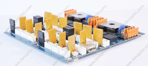
5-in-1 antenna PCBA assembly usually includes RF connectors, wireless modules, small matching components, shielding parts, and coaxial cables. These areas need tighter process control.

RF Connectors

  • Check connector position, solder quality, grounding, mechanical strength, and cable plugging direction. U.FL and IPEX connectors are small and can be damaged by poor soldering or repeated rework.

Wireless Modules

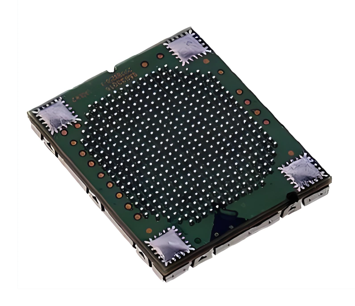
  • Check solder paste volume, stencil opening, reflow profile, placement accuracy, and inspection method. LGA, BGA, castellated, and fine-pitch wireless modules need stable SMT control.

Matching Network Components

  • Small capacitors and inductors near RF paths must match the BOM and placement file. Wrong values or wrong positions can change RF behavior.

Shielding Cans

  • Shielding only works well when grounding and soldering are reliable. Shielding can footprints, solder paste openings, and inspection standards should be confirmed before assembly.

Coaxial Cables and Wire Harnesses

  • Cable direction, bend radius, connector locking, strain relief, and final assembly sequence should be checked before batch production.

First Article Inspection

  • For the first build, inspect connector placement, module alignment, component value, polarity, solder joints, shielding position, and test results before moving to larger quantities.
5-in-1 Antenna

What Testing Should Be Planned Before Shipment?

Testing should be defined before assembly, not after production is finished.

TestPurpose
Bare PCB electrical testCheck opens and shorts
Impedance testConfirm RF trace impedance on test coupon
AOICheck solder joints, polarity, missing parts
X-rayInspect BGA/LGA or hidden solder joints
Functional testConfirm power, module boot, interface communication
RF path continuity checkFind connector or soldering issues
GNSS/Wi-Fi/cellular function checkVerify product-level wireless function
Final assembly inspectionCheck cable, connector, enclosure, label, and package

A PCB/PCBA factory can support production-level tests such as electrical test, impedance test, AOI, X-ray, visual inspection, and functional testing based on customer procedures.

Advanced antenna tests such as OTA, radiation pattern, antenna efficiency, and certification-level RF performance usually require customer fixtures, RF chambers, or third-party labs.

What Files Are Needed for a Faster Quote?

Complete files help the manufacturer review the project faster and quote more accurately.

Send:

  • Gerber or ODB++ files
  • Drill files
  • PCB stackup
  • Controlled impedance requirement
  • BOM with manufacturer part numbers
  • Pick-and-place file
  • Assembly drawing
  • RF connector datasheets
  • Wireless module datasheets
  • Antenna specification
  • Testing requirements
  • Cable or wire harness requirements
  • Order quantity
  • Target delivery schedule

For PCBA projects, BOM quality matters. RF connectors, wireless modules, EOL parts, and alternative components should be checked before batch production.

FAQs About 5-in-1 Antenna PCB and PCBA Manufacturing

Q1: Can a PCB/PCBA manufacturer design the 5-in-1 antenna?
Usually no. A PCB/PCBA manufacturer supports layout review, DFM, impedance control, fabrication, assembly, and testing. Full antenna electromagnetic design should be handled by RF antenna specialists.

Q2: Does a 5-in-1 antenna PCB need controlled impedance?
In most cases, yes. GNSS, cellular, and Wi-Fi RF feed lines commonly require 50Ω controlled impedance.

Q3: Can FR4 be used for 5-in-1 antenna products?
Yes, FR4 can be used when the frequency, loss requirement, and layout structure are suitable. For higher-frequency or lower-loss paths, high frequency PCB materials may be needed.

Q4: What is the most common manufacturing issue?
Common issues include unclear impedance notes, incorrect RF connector footprints, poor grounding, missing assembly clearance, wrong matching components, and poor cable routing.

Q5: What PCB type is commonly used?
Many projects use multilayer controlled impedance PCB. Compact wireless products may use HDI PCB or rigid-flex PCB.

Q6: Can the factory test RF performance?
The factory can support production-level tests. Advanced RF performance testing may require customer fixtures, RF chambers, or third-party RF labs.

In summary, a 5-in-1 antenna product is not difficult only because it uses several wireless functions. The real production challenge is making the PCB and PCBA stable, repeatable, and testable.

Before production, customers should confirm RF trace impedance, stackup, connector footprint, assembly clearance, shielding parts, cable routing, BOM accuracy, and test method. These checks help reduce rework, shorten debugging time, and improve batch consistency.

Best Technology supports RF PCB, high frequency PCB, controlled impedance PCB, multilayer PCB, HDI PCB, rigid-flex PCB, ceramic PCB, metal core PCB, PCB fabrication, PCBA assembly, SMT stencil, wire harness, component sourcing, DFM review, and production testing.

Send your Gerber files, BOM, antenna specification, and project requirements to sales@bestpcbs.com. Our engineering team can review your 5-in-1 antenna PCB and PCBA project before production and help you move from prototype to a more stable manufacturing build.

You may also like

Billboard Defect in SMT: Is Your PCBA Supplier Controlling It Properly?
Thursday, May 21st, 2026

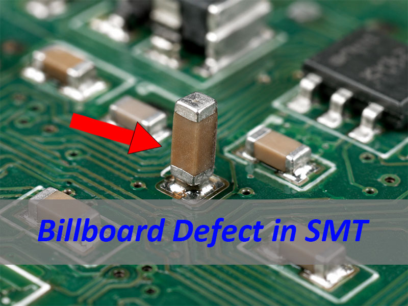
Billboard defect in SMT is a side-standing chip component defect that happens when a resistor, capacitor, or other small SMD part does not lie flat on the PCB pads after reflow soldering. The part may still touch the pads, but the solder joint is not formed in the correct position. This can raise concerns about electrical contact, mechanical strength, IPC acceptance, and long-term PCBA reliability.

This article explains what billboard defect in SMT means, how it differs from tombstone defect, whether it can be accepted under IPC workmanship standards, why it happens, and how a professional PCBA supplier should inspect and prevent it. The goal is not only to explain the defect, but also to help engineers, buyers, and quality teams judge whether their SMT assembly process is being controlled properly.

EBest Circuit (Best Technology) provides PCB fabrication, component sourcing, SMT assembly, PCBA manufacturing, testing, and box-build assembly support for customers from prototype to mass production. If you are preparing a PCB or PCBA project and want to reduce SMT assembly risks before production, please contact us at sales@bestpcbs.com.

billboard defect in smt

What Is Billboard Defect in SMT?

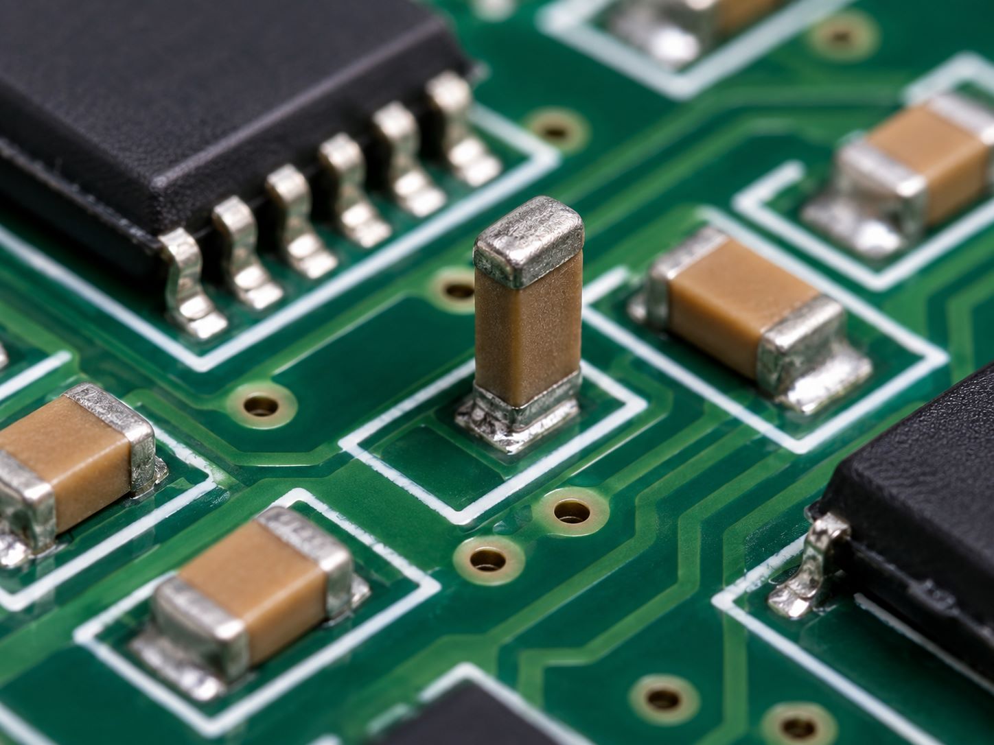
Billboard defect in SMT happens when a chip component stands on its side instead of lying flat on the PCB pads. The part looks like a small signboard, so this defect is often called billboarding or side stand.

It often appears on small chip resistors and capacitors. It is more common with 0402, 0201, and 01005 parts. These parts are light, small, and easy to move during solder reflow.

A billboarded part may still touch the pads. So, the board may pass a basic electrical test. But this does not mean the solder joint is reliable.

The contact area may be small. The solder joint may be weak. The part may fail later during vibration, heat cycling, handling, or final product use.

That is why a PCBA supplier should not treat billboard defect as a simple visual issue. It needs proper inspection, root cause analysis, and process control.

billboard defect in smt

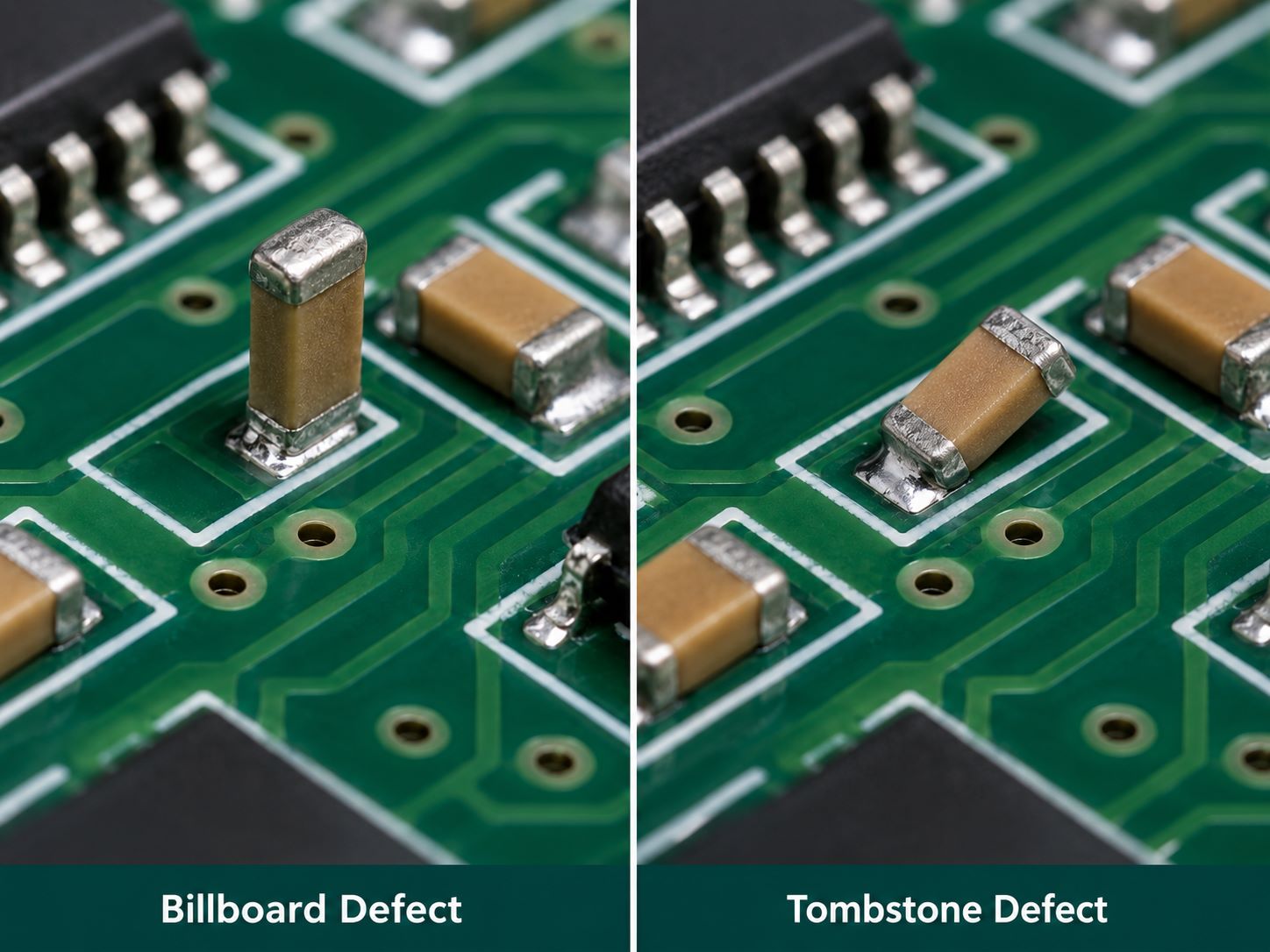
Billboard Defect vs Tombstone Defect: What Is the Difference?

Billboard defect and tombstone defect are often confused. Both can happen during SMT assembly, but they are different defects.

ItemBillboard DefectTombstone Defect
AppearanceComponent stands on its sideOne end lifts from the pad
Common nameSide standDrawbridge
Electrical riskMay still conductOften causes an open circuit
Main concernWeak solder jointDirect functional failure
Typical judgmentNeeds further reviewUsually more serious

A tombstone defect usually means one end of the component has lifted away from the pad. This often creates an open circuit.

A billboard defect may still have contact with the pads. However, the solder joint is not formed as designed. The board may work during testing, but the joint may not survive long-term use.

This difference matters. A supplier should not mix these two defects in a quality report. The wrong defect name can lead to the wrong corrective action.

billboard defect in smt

Is Billboard Defect in SMT Acceptable Under IPC Standards?

IPC-A-610 is widely used to judge PCBA workmanship. It helps define what is acceptable, what is a process indicator, and what is a defect.

However, billboard defect should not be judged by one simple rule. The final decision depends on several factors:

  • Product class
  • Customer standard
  • Component size
  • Defect quantity
  • Solder contact condition
  • Mechanical strength
  • Circuit function
  • Product application

For example, a low-risk consumer product and a medical control board should not be judged in the same way. Automotive, aerospace, medical, industrial, and communication products often need stricter control.

A key point is this: passing an electrical test does not always mean the defect is acceptable.

A billboarded part may still conduct electricity. But if the solder joint is weak, it can become a field failure risk.

A responsible supplier should provide clear evidence before asking the customer to accept the board. Useful evidence includes AOI images, defect location, affected quantity, IPC judgment basis, test results, and corrective action.

Why Does Billboard Defect Happen During SMT Assembly?

Billboard defect usually comes from imbalance. The imbalance may come from PCB design, solder paste, placement, reflow, or material quality.

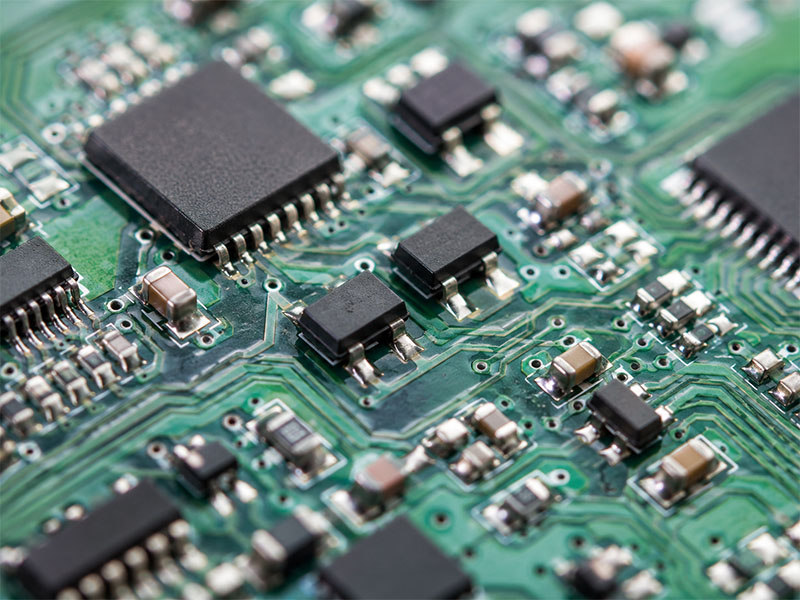
Uneven pad design

  • If one pad connects to a large copper area and the other pad connects to a thin trace, both sides heat at different speeds. One end may wet faster than the other. This can pull the part into the wrong position.
Unbalanced solder paste volume

  • If one pad gets more solder paste than the other, the solder force becomes uneven. Small chip parts can rotate, lift, or stand on their side during reflow.

Poor stencil design

  • Stencil openings control solder paste volume. If the aperture size or shape is not suitable, the paste deposit may become unbalanced. This is a common risk for small passive components.

Placement offset

  • Small SMT parts need accurate placement. If the part is not centered on both pads, reflow may not correct the position. In some cases, it can make the defect worse.

Unsuitable reflow profile

  • A fast heating rate or short soak time can create uneven wetting. One side may melt and pull first, while the other side is not ready. This can cause billboarding or tombstoning.

Poor solderability

  • Oxidized component terminals or PCB pads can also cause uneven wetting. Old parts, poor storage, or exposed reels may increase this risk.

How to Find the Root Cause of Billboard Defect in SMT?

A good PCBA supplier should not only say, “This is an SMT issue.” They should find the real cause.

Area to CheckWhat It May Show
PCB designUneven pads, large copper connection, missing thermal relief
Stencil designUneven solder paste volume
Solder paste printingPaste offset, paste height issue, poor release
Placement processOffset, wrong nozzle, feeder instability
Reflow profileFast ramp rate, weak soak stage, uneven heating
Material conditionOxidation, poor solderability, bad storage
AOI dataRepeated defect at the same location

The most useful question is:

Is this an isolated defect or a repeated process problem?

If the same location fails again and again, the issue may come from pad design, copper balance, or stencil opening.

If the defect appears randomly, the cause may be paste printing, placement, reflow, or material control.

This matters because it helps define the next action. A design issue may need a Gerber change. A printing issue needs stencil or process adjustment. A solderability issue needs material review.

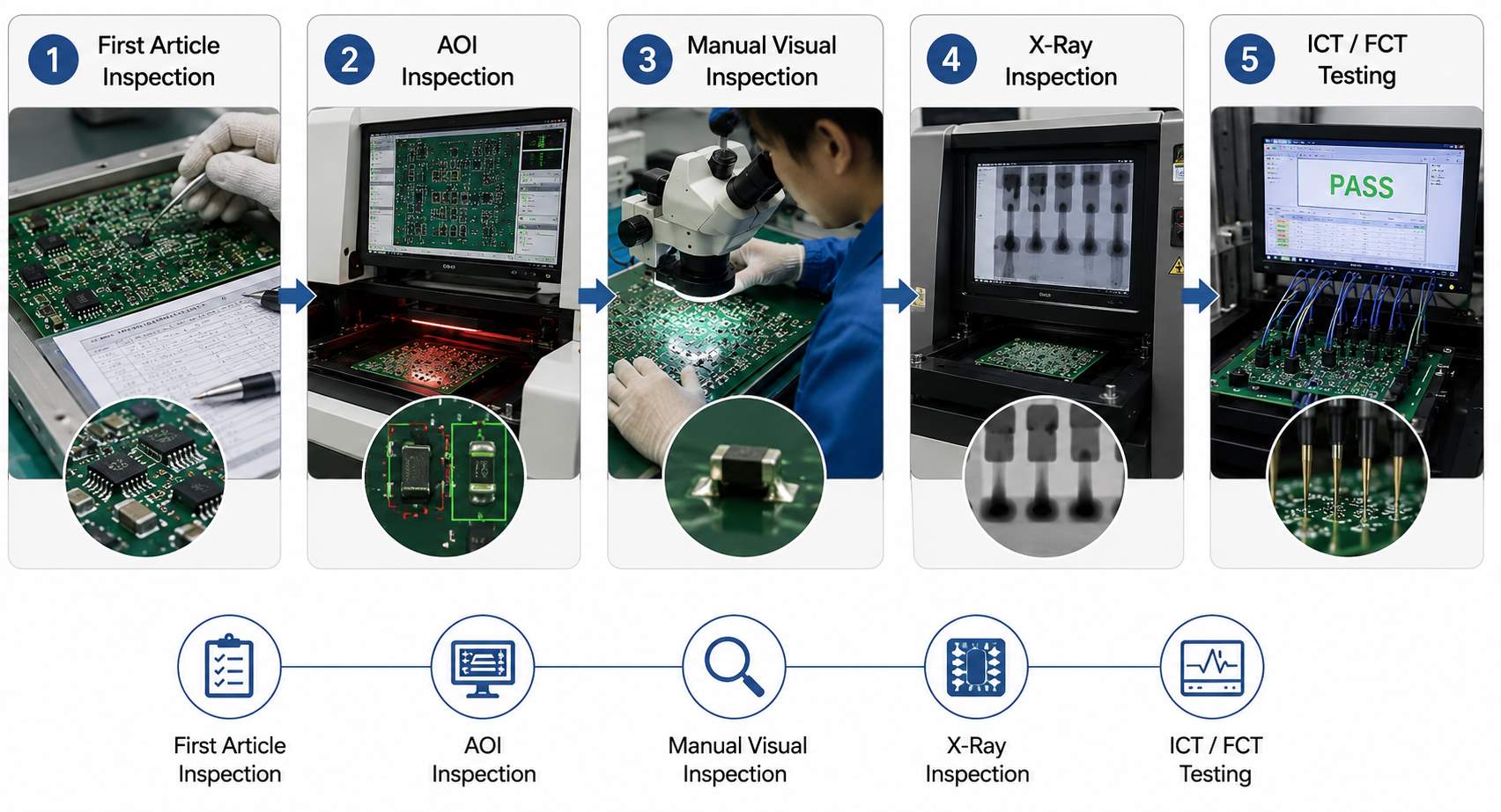
How Can EBest Circuit (Best Technology) Inspect Billboard Defect Before Shipment?

EBest Circuit (Best Technology) uses several inspection steps to reduce the risk of SMT defects before shipment.

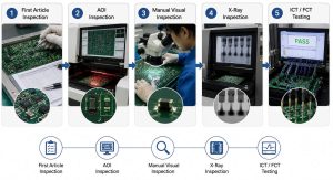
First article inspection

  • Before batch production, we check component value, position, polarity, orientation, and soldering condition. This helps find problems before they affect the full lot.

AOI inspection

  • AOI is one of the main tools for finding billboard defect in SMT production. It can detect side-standing parts, missing parts, offset, skew, polarity errors, solder bridging, and poor solder joints.

Manual visual inspection

  • For uncertain AOI results, trained inspectors review the board with magnification and proper lighting. This helps confirm real defects and reduce false calls.

X-Ray inspection

  • X-Ray is mainly used for hidden solder joints, such as BGA, QFN, and LGA. For normal chip resistors and capacitors, AOI and visual inspection are usually more direct. Still, X-Ray is important for full PCBA quality control when hidden joints are present.

ICT and FCT testing

  • ICT and FCT can find open circuits, shorts, wrong values, and function problems. But they cannot replace visual inspection.

A billboarded component may pass electrical testing. Yet the solder joint may still be weak. That is why visual inspection and electrical testing should work together.

billboard defect in smt

How Does Billboard Defect Affect Electrical Performance and Long-Term Reliability?

Billboard defect may not cause instant failure. That is why it can be risky.

A side-standing part may still conduct. But the solder joint is not normal. The contact area may be small, and the joint may have lower strength.

This can lead to:

  • Higher contact resistance
  • Unstable electrical contact
  • Weak mechanical strength
  • Solder joint cracking
  • Failure during vibration
  • Failure after thermal cycling
  • Open circuit during field use

The risk is higher in products that face heat, vibration, shock, or long service life. This includes automotive electronics, industrial controllers, medical devices, outdoor equipment, power products, and communication systems.

So the right question is not only:

Does the board work now?

The better question is:

Will the board stay reliable in real use?

How Can SMT Assembly Prevent Billboard Defect from Happening Again?

Prevention should start before SMT production. A reliable supplier should control both design and process factors.

DFM review

  • Check pad size, pad symmetry, copper balance, solder mask opening, and component spacing. If one pad connects to a large copper area, thermal relief may be needed.

Stencil optimization

  • Control solder paste volume on both pads. For small chip components, more paste is not always better. Balanced paste is more important.
Stable paste printing

  • Control stencil cleaning, squeegee pressure, printing speed, paste condition, and PCB support. Good printing helps reduce solder imbalance.

Accurate placement

  • Use the correct nozzle, feeder setup, component library, and placement data. Small parts need tighter placement control.

Proper reflow profile

  • Avoid heating too fast. Give both sides of the component enough time to reach a balanced temperature. Adjust the profile based on board thickness, copper area, and component density.

Material control

  • Store PCBs and components correctly. Prevent oxidation and moisture issues. Review old or exposed components before production.


AOI trend review

  • AOI should not only catch defects. It should also help engineers find patterns. If the same location fails again, the team should review design, stencil, placement, and reflow together.

Why Choose EBest Circuit (Best Technology) for Reliable SMT Assembly and PCBA Manufacturing?

Customers searching for billboard defect in SMT usually need more than a definition. They need a supplier who can prevent the issue, inspect it, explain it, and fix it.

EBest Circuit (Best Technology) provides one-stop PCB and PCBA manufacturing support. Our services include PCB fabrication, component sourcing, SMT assembly, through-hole assembly, testing, and box-build assembly.

We support customers from prototype to mass production. Our team can review Gerber files, BOMs, assembly drawings, and test requirements before production.

Our PCBA support includes:

  • DFM review before production
  • PCB fabrication and PCBA assembly
  • Component sourcing support
  • SMT process control
  • AOI, X-Ray, ICT, and FCT testing
  • Engineering support for defect analysis
  • Prototype and batch production support
  • Quality control for demanding applications

For billboard defect, tombstone defect, solder bridging, poor wetting, and other SMT issues, our team reviews the issue from design, material, and process angles.

This helps customers reduce repeat defects, improve shipment quality, and build more reliable electronic products.

To sum up, billboard defect in SMT is not only a small visual issue. It can reflect pad design imbalance, solder paste variation, placement offset, reflow profile problems, or material solderability issues. For PCBA projects, the best approach is to prevent this defect before production through proper DFM review, stable SMT process control, and reliable inspection.

If your next PCB or PCBA project requires careful SMT assembly control, EBest Circuit (Best Technology) can support your project from early manufacturing review to final assembly and testing. To discuss your PCB fabrication or PCBA assembly requirements, contact us at sales@bestpcbs.com.

FAQs About Billboard Defect in SMT

1. Is billboard defect the same as tombstoning?

No. Billboard defect means the component stands on its side. Tombstoning means one end lifts from the pad. Tombstoning usually has a higher open-circuit risk.

2. Can a billboarded component pass electrical testing?

Yes. It may still touch the pads and pass testing. But the solder joint may still be weak. Visual inspection and reliability review are still needed.

3. Is billboard defect acceptable under IPC-A-610?

It depends on product class, component size, quantity, location, customer standard, and actual solder condition. The supplier should provide inspection evidence before making a judgment.

4. What causes billboard defect in SMT?

Common causes include uneven pad design, poor stencil design, unbalanced solder paste, placement offset, poor reflow profile, and weak solderability.

5. Which components are more likely to have billboard defect?

Small chip resistors and capacitors are more likely to have this defect. 0402, 0201, and 01005 packages need careful process control.

6. Can billboard defect be repaired?

Yes. Skilled technicians can repair it with proper tools and controlled heating. After repair, the board should go through visual inspection and electrical testing again.

7. How can a PCBA supplier prevent billboard defect?

The supplier should use DFM review, proper stencil design, stable solder paste printing, accurate placement, suitable reflow profile, and AOI inspection.

8. Why should customers care if the board still works?

Because the solder joint may be weak. The board may pass testing now but fail later during vibration, heat cycling, handling, or field use.

9. What should I ask my PCBA supplier about this defect?

Ask for the defect location, inspection images, IPC judgment basis, root cause, affected quantity, repair plan, and prevention action.

If you are preparing a PCB or PCBA project and want to reduce SMT assembly risks such as billboard defect, tombstoning, solder bridging, or poor wetting, EBest Circuit (Best Technology) can support you from the manufacturing stage. Our team can review your Gerber files, BOM, assembly drawings, and production requirements before PCB fabrication and PCBA assembly, helping you improve manufacturability and reduce avoidable process issues.

For PCB manufacturing, PCBA assembly, DFM review, component sourcing, and testing support, please contact us at sales@bestpcbs.com.

You may also like

Transistor Pinout Guide for PCB Layout and PCBA Assembly
Wednesday, May 13th, 2026

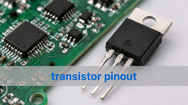
A transistor pinout shows how the pins of a transistor are arranged in its physical package. For a BJT transistor, these pins are usually Emitter, Base, and Collector. For PCB layout and PCBA assembly, this small detail is very important. It affects the schematic, footprint, SMT placement, BOM review, and final circuit performance.

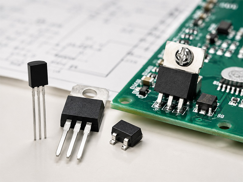
At first glance, a transistor looks simple. It may only have three pins. However, the same transistor family can come in several packages, such as TO-92, SOT-23, TO-220, SOT-223, or DFN. In addition, different manufacturers may use different pin arrangements for similar-looking parts.

Therefore, engineers should confirm the transistor pinout before PCB layout starts. They should also check it again before SMT assembly. This helps reduce footprint errors, wrong part orientation, and avoidable production issues.

This guide explains transistor pinout from a PCB and PCBA point of view. It is written for engineers, hardware teams, purchasing teams, and product companies that need reliable PCB manufacturing and assembly.

transistor pinout

What Is a Transistor Pinout?

A transistor pinout is the physical order of the transistor pins. It tells you which lead or pad connects to each internal function of the device.

For a BJT transistor, the three main pins are:

Pin NameShort NameMain Function
EmitterEWorks as one side of the main current path
BaseBControls the transistor switching or amplification
CollectorCConnects to the load or output side in many circuits

For PCB design, the transistor pinout must match three things:

  • The schematic symbol
  • The PCB footprint
  • The actual component package

If these three parts match, the circuit has a much better chance of working correctly after assembly. However, if one part is wrong, the finished PCB may fail during testing.

For example, a TO-92 transistor may look the same as another TO-92 transistor. Even so, the pin order may be different. One part may use E-B-C order, while another may use C-B-E order. Because of this, engineers should not rely only on the package shape.

Instead, the safest method is to check the official datasheet. Then, compare the datasheet pinout with the PCB library footprint.

Why Does Transistor Pinout Matter in PCB Layout and PCBA Assembly?

Transistor pinout matters because it affects how the real part connects to the circuit. In a PCB file, the footprint may look correct. During SMT assembly, the component may also be placed neatly. However, the circuit can still fail if the footprint pin mapping is wrong.

In PCB layout, transistor pinout affects routing, pad numbering, copper layout, and test point planning. In PCBA assembly, it affects pick-and-place rotation, AOI inspection, and functional testing.

For instance, an SOT-23 transistor has a very small body and three pads. The package looks simple. Yet the electrical pin order is not always the same for every part. As a result, one wrong footprint can cause many assembled boards to fail.

A correct transistor pinout helps avoid:

  • Wrong PCB footprint selection
  • Incorrect schematic-to-layout mapping
  • SMT orientation errors
  • NPN and PNP part mix-ups
  • Wrong alternative transistor selection
  • Failed functional testing after assembly
  • Extra rework during pilot production

Therefore, pinout checking should be part of the normal DFM review process. It is a small step, but it helps protect the full PCB production flow.

For EBest Circuit projects, this type of check connects directly with PCB fabrication, SMT assembly, BOM review, DFM support, and turnkey PCBA production.

What Do Emitter, Base, and Collector Mean in a BJT Transistor Pinout?

In a BJT transistor pinout, the three pins are Emitter, Base, and Collector. Each pin has a different role in the circuit.

BJT PinShort NameWhat It DoesPCB Design Note
EmitterEConnects to one side of the current pathMust match the expected current direction
BaseBControls the transistorUsually needs a proper resistor
CollectorCOften connects to the load sideRouting should follow the circuit design

The Base is the control pin. A small signal at the Base can control a larger current between the Collector and Emitter. Because of this, BJT transistors are widely used for switching and amplification.

However, the physical pin order can be different from what beginners expect. A schematic symbol may show the Base in the middle. Still, the actual transistor package may not place the Base on the middle lead.

For that reason, engineers should always check the package drawing. They should also confirm the view direction. Some datasheets show the front view, while others show the bottom view. This detail is easy to miss during library creation.

In short, knowing Emitter, Base, and Collector is only the first step. The more important step is making sure these pins are mapped correctly to the PCB pads.

How to Determine Transistor Pinout Before PCB Design?

The best way to determine transistor pinout before PCB design is to check the official datasheet. Then, compare the datasheet with the schematic symbol, PCB footprint, and BOM part number.

A simple engineering workflow is shown below:

StepWhat to CheckWhy It Matters
1Full part numberSimilar part names may have different packages
2Manufacturer datasheetIt gives the most reliable pinout data
3Package drawingPin order depends on the viewing direction
4Schematic symbolPin names must match the real transistor
5PCB footprintPad numbers must connect to the correct pins
6BOM alternativesSubstitute parts may use different pinouts
7SMT orientationPlacement data must match the package direction

This process is useful for both through-hole and SMD transistors. However, it becomes even more important for SMT assembly. Small packages leave little room for visual correction after placement.

Also, engineers should check the complete ordering code. A short part name may not be enough. For example, one transistor family may include TO-92, SOT-23, and metal-can versions. Although the electrical function may be similar, the package pinout can be different.

Before releasing Gerber files, the design team should review the pinout together with the footprint. In addition, the assembly team should check the pick-and-place file before SMT production.

This habit saves time. More importantly, it helps the project move smoothly from prototype to batch production.

NPN Transistor Pinout vs PNP Transistor Pinout: What Should Engineers Check?

NPN and PNP transistors both use Emitter, Base, and Collector pins. However, their current direction and circuit polarity are different. Therefore, engineers must check both the transistor type and the physical pinout.

ItemNPN TransistorPNP Transistor
Symbol arrowPoints outwardPoints inward
Common useLow-side switchingHigh-side switching
Control styleTurns on with positive base driveTurns on with negative base drive
PCB check pointCollector load path and base resistorEmitter supply path and polarity
Assembly concernMay look similar to PNP partsRequires clear BOM control

In PCB projects, an NPN transistor and a PNP transistor may use the same package shape. For example, both can be supplied in SOT-23 or TO-92 packages. As a result, the assembly line may not easily tell the difference by shape alone.

Because of this, BOM accuracy is very important. The approved manufacturer part number should be clear. The reference designator should also match the correct transistor type.

In addition, substitute parts should be reviewed carefully. A replacement transistor must match the package, pinout, polarity, voltage rating, current rating, and power rating.

For PCBA assembly, clear documentation is helpful. Assembly drawings, centroid data, and BOM files should all point to the same part direction. This makes SMT production more stable and easier to inspect.

How Do SMD Transistor Pinouts Affect SMT Placement?

SMD transistor pinouts affect SMT placement because the part is mounted by pad position and rotation angle. If the footprint is wrong, the SMT machine can still place the part correctly from a mechanical view. However, the circuit connection may still be wrong.

SOT-23 is one of the most common SMD transistor packages. It is small, easy to place, and widely used in compact PCB designs. Even so, SOT-23 pinouts are not universal. Different devices may use different pin mapping in the same package outline.

SMD PackageCommon UseSMT Placement Note
SOT-23Small-signal switchingCheck Pin 1 and footprint mapping
SOT-223Medium-power applicationsReview copper area and heat path
SOT-89Power and regulator-style circuitsCheck pad size and thermal design
DFN / QFN-style packagesCompact circuit designsConfirm hidden pad and stencil design

During SMT assembly, the pick-and-place machine follows the centroid file. It places the part according to X-Y position and rotation. However, it does not know whether the electrical pinout is right.

Therefore, engineers should check several files before production:

  • Datasheet package drawing
  • CAD footprint pad numbering
  • Pick-and-place rotation
  • Assembly drawing
  • BOM manufacturer part number
  • AOI inspection reference
  • Approved vendor list

In addition, SMD transistors often have small top markings. These markings can be different between suppliers. For this reason, the production team should not rely only on the code printed on the package.

A good DFM review can catch many of these risks before PCB fabrication and SMT assembly begin.

What Is the 2N2222 Transistor Pinout and 2N2222A Pinout?

The 2N2222 transistor pinout depends on the exact package and manufacturer. The 2N2222 and 2N2222A are common NPN BJT transistors. They are often used for switching and amplification. However, their physical pinout should still be checked before PCB layout.

The 2N2222 family is available in several forms. Some versions use metal-can packages. Others use plastic through-hole packages or SMD packages. Because of this, one footprint cannot cover every version.

Part NumberTypeCommon PackagePCB Design Note
2N2222NPN BJTTO-18, TO-92, SMD variantsConfirm the package-specific pinout
2N2222ANPN BJTTO-18, TO-92, SMD variantsCheck supplier datasheet
PN2222ANPN BJTTO-92Common plastic-package version
MMBT2222ANPN BJTSOT-23Common SMT version

For PCB projects, 2N2222 is a useful example of why full part control matters. A schematic may simply list “2N2222.” Later, purchasing may source a different package version. If the PCB footprint was made for another package, the assembly may face problems.

A better practice is to define the exact manufacturer part number in the BOM. Also, the package name and footprint name should be clear. If alternatives are allowed, each alternative should be checked before approval.

This is especially important when moving from prototype to mass production. During early samples, engineers may use a through-hole part. Later, they may switch to an SMT version for volume assembly. In that case, the PCB footprint and pinout must be reviewed again.

What Are Common Transistor Pinout Examples for PCB Projects?

Common transistor examples help engineers compare package types and layout notes. However, the final design should always follow the original datasheet.

Part NumberTypeCommon PackageTypical UsePCB / PCBA Note
2N2222 / 2N2222ANPN BJTTO-18, TO-92, SOT-23 variantsSwitching and amplificationConfirm package version
2N3904NPN BJTTO-92, SOT-23 variantsLow-current switchingCommon signal transistor
2N3906PNP BJTTO-92, SOT-23 variantsComplementary switchingCheck polarity and pin mapping
BC547NPN BJTTO-92General amplificationPin order may differ from 2N series
BC557PNP BJTTO-92Low-power switchingOften paired with BC547-style circuits
S8050NPN BJTTO-92, SMD variantsLow-power switchingConfirm supplier pinout
S8550PNP BJTTO-92, SMD variantsComplementary transistorOften used with S8050
BD139NPN BJTTO-126Medium-power circuitsThermal layout should be reviewed
BD140PNP BJTTO-126Complementary power stageCheck heat path and package
TIP120NPN DarlingtonTO-220Higher-current switchingReview thermal design
MMBT3904NPN BJTSOT-23SMT signal switchingOrientation is critical
MMBT3906PNP BJTSOT-23SMT signal switchingCheck approved alternatives
MRF9120RF power transistorRF power packageRF power circuitsFollow datasheet and RF layout rules

This table is useful during early component selection. Still, it should not replace datasheet checking. Similar transistor names can have different package versions. Also, the same electrical type may be sold by several manufacturers.

For production PCB projects, it is better to build an approved component list. This list should include the part number, package, footprint, supplier, and substitute options. As a result, the design team and purchasing team can work with the same information.

In addition, PCB and PCBA teams should review transistor pinout before manufacturing. This review is useful for both prototype builds and batch orders.

What Transistor Pinout Mistakes Can Cause PCB Assembly Defects?

Transistor pinout mistakes can lead to PCB assembly defects, even when PCB fabrication and SMT placement are well controlled. Most of these issues come from wrong library data, unclear BOM information, or unverified substitute parts.

MistakePossible ResultPrevention Method
Wrong footprint selectedPads connect to the wrong pinsCompare footprint with datasheet
Generic symbol usedSymbol pins do not match the packageUse verified library mapping
Substitute part has a different pinoutCircuit may not work as plannedCheck AVL and approved alternatives
SMD orientation is wrongPart is placed at the wrong angleReview centroid file and assembly drawing
TO-92 pin order is assumedThrough-hole pins connect incorrectlyConfirm package view and lead order
NPN and PNP are mixedCircuit function changesStrengthen BOM review
Thermal design is ignoredPower device runs too hotReview copper area and heat path
RF transistor layout is treated as standardRF performance may become unstableFollow datasheet layout guidance

Fortunately, most of these problems can be found before production. The key is to review the design early.

Before PCB fabrication, engineers should check the schematic, footprint, package drawing, and BOM. Before SMT assembly, the production team should check placement direction, part marking, and assembly files. After assembly, AOI and functional testing can confirm the result.

For turnkey PCBA projects, this process is even more important. A small transistor error can affect the whole batch. Therefore, early review helps improve delivery speed and production quality.

EBest Circuit supports customers with PCB fabrication, SMT assembly, component sourcing, BOM review, DFM pre-check, testing, and turnkey electronics manufacturing. For transistor-based circuits, our engineering team can help check package selection, footprint consistency, assembly orientation, and production feasibility before batch manufacturing.

All in all, a transistor pinout may look like a small detail. However, it plays a large role in PCB layout and PCBA assembly. When the pinout is correct, the schematic, footprint, BOM, and SMT data can work together smoothly.

Before releasing a PCB design, engineers should check the official datasheet, package drawing, pin numbering, footprint mapping, and approved alternatives. In addition, they should review SMD orientation and substitute parts before assembly.

This is especially useful for SOT-23 transistors, 2N2222 variants, NPN and PNP substitutions, and production projects with BOM changes.

With careful pinout verification, electronic product teams can reduce assembly risk and move from prototype to mass production with more assurance. EBest Circuit helps customers with PCB manufacturing, SMT assembly, component sourcing, DFM review, BOM optimization, and testing, supporting a smoother path from design files to reliable assembled boards. If any questions, pls feel free to contact us at sales@bestpcbs.com.

FAQs About Transistor Pinout

1. What is a transistor pinout?

A transistor pinout shows the physical order of a transistor’s pins. For a BJT transistor, these pins are usually Emitter, Base, and Collector. In PCB layout and PCBA assembly, the pinout must match the schematic symbol, PCB footprint, and actual component package.

2. How do I determine the correct transistor pinout?

The safest way is to check the official manufacturer datasheet. Engineers should confirm the full part number, package type, pin numbering, and viewing direction. Then, they should compare this information with the schematic symbol and PCB footprint before releasing the design.

3. Are all transistors with the same package pinout the same?

No. Transistors with the same package, such as TO-92 or SOT-23, may have different pin arrangements. For example, one TO-92 transistor may use E-B-C order, while another may use C-B-E. Therefore, package shape alone is not enough for PCB design.

4. Why is transistor pinout important for PCBA assembly?

Transistor pinout affects SMT placement, solder pad mapping, BOM verification, and functional testing. If the pinout does not match the PCB footprint, the component may be assembled correctly in appearance but fail electrically. That is why pinout verification should be included in DFM review before PCB fabrication and assembly.

You may also like

10 Common Components on a PCBA for Beginners
Wednesday, September 4th, 2024

Even though we live in a world full of electronic gadgets, electronic devices are still shrouded in mystery. The working principle of electronic projects may seem very abstract, as the interior of these gadgets does not seem to have any visible mechanical parts. There are no moving parts such as gears or shafts on the printed circuit board, nor any significant visual changes.

The flow of electricity is invisible and can only be perceived by the effect it produces. Therefore, for those who want to dabble in the field of electronics making, making electronics as a hobby can seem like an extremely challenging task. It seems hard to imagine building something without fully understanding the principles behind it.

What does PCBA mean?

PCBA is the abbreviation of Printed Circuit Board Assembly, which refers to the process of welding, inserting, etc. of electronic components to the circuit board, and welding, inserting, etc. PCBA is an indispensable and important link in the manufacture of electronic products, which directly affects the performance stability and service life of electronic products.

The manufacturing process of PCBA mainly includes components mounting, welding, post-welding processing and functional testing. The first is the component mounting, which is a process of welding the patch components, plug-in components, etc., to the PCB. Then there is welding, through traditional wave soldering or modern lead-free welding and other methods, the components are firmly fixed on the PCB. After that, the welding process is mainly to remove the welding slag on the PCBA surface, clean the PCBA surface, and check the solder joints and components of PCBA. Finally, the functional test is carried out, which is the last step in the PCBA process, and the PCBA is fully functional tested by various test equipment to ensure the stability and reliability of PCBA.

Applications of PCBA

PCBA products are widely used in various electronic products, such as household appliances, communication equipment, automotive electronics, industrial control equipment, etc.  You can see it everywhere.

Different electronic products have different requirements for PCBA. Some require PCBA to be small and exquisite, some require PCBA to be high temperature and high pressure resistant, and some require PCBA to be waterproof and dustproof. With the rapid development of 5G, artificial intelligence, Internet of Things and other fields, PCBA will be more widely used, and PCBA’s performance and reliability requirements will also be higher.

Common components on a PCBA and their symbols

1. Resistor

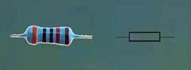
    Resistors are one of the most commonly used electronic components in PCBA, used to limit the current in the circuit. According to different materials, structures, and resistance values, resistors can be divided into fixed resistors, variable resistors, and special resistors. Resistors are widely used in various circuits, such as power circuits, amplification circuits, signal processing circuits, etc., to achieve current regulation and control.

    2. Capacitor

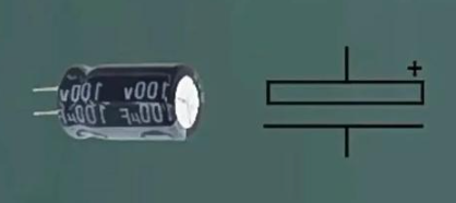
    A capacitor is a component that stores charge and electrical energy, with the characteristic of blocking direct current and passing alternating current. In PCBA, capacitors are commonly used in circuits such as filtering, coupling, tuning, and bypassing to improve circuit performance and stability. According to their different structures and applications, capacitors can be divided into fixed capacitors, variable capacitors, and fine tuned capacitors.

    3. Inductor

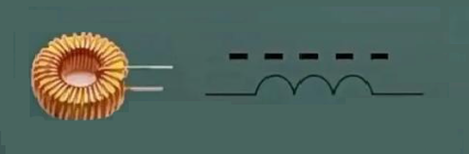
    Inductor, also known as induction coil, has the function of storing magnetic energy. In circuits, inductors can prevent changes in current and play a role in filtering and stabilizing the current. Inductance has a wide range of applications in power filtering, signal processing, and other fields.

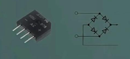
    4. Diode

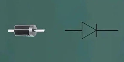
    A diode is an electronic component with unidirectional conductivity, widely used in circuits such as rectification, detection, and voltage regulation. In PCBA, diodes can achieve functions such as voltage regulation, signal amplification, and switch control in the circuit. Common diodes include silicon diodes and germanium diodes, whose performance parameters such as forward voltage drop and reverse breakdown voltage determine their application scenarios.

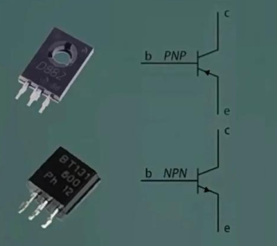
    5. Transistor

    Transistors are electronic components with functions such as amplification and switching, and are the core components that make up various circuits. In PCBA, transistors are commonly used in amplification circuits, oscillation circuits, switch circuits, etc. to achieve signal amplification, frequency conversion, and circuit control. There are many types of transistors, including bipolar transistors, field-effect transistors, etc., each with its own characteristics, widely used in various electronic devices.

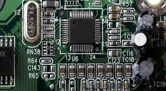
    6. IC Integrated circuit

    Integrated circuit is an electronic component that integrates multiple electronic components on a single chip, with advantages such as small size, low power consumption, and stable performance. In PCBA, integrated circuits are key components for implementing various complex functions, such as digital signal processing, analog signal processing, communication interfaces, etc. Common integrated circuits include operational amplifiers, logic gate circuits, microprocessors, etc., which are widely used in various intelligent devices and systems.

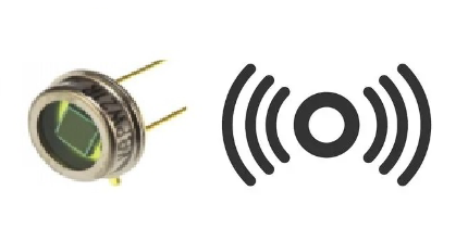
    7. Sensor

    Sensors can sense physical quantities or states in the environment and convert them into electrical signals for output. In PCBA, sensors are commonly used to detect parameters such as temperature, humidity, light, pressure, etc., providing data support for intelligent control of electronic devices. There are various types of sensors with different performances, and choosing the appropriate sensor is crucial for improving the performance and user experience of electronic devices.

    8. Controllable silicon rectifier (SCR)

    Also known as thyristors, silicon controlled rectifiers (SCR) are similar to transistors and diodes – their working principle is essentially the coordinated operation of two transistors. Although SCR also has three pins, they are composed of four layers of silicon material instead of three layers, and are only used as switches, not amplifiers. Unlike single transistors that require continuous current to remain on, SCR only requires one pulse to activate the switch. They are very suitable for converting large amounts of electricity.

    9. Crystal oscillator

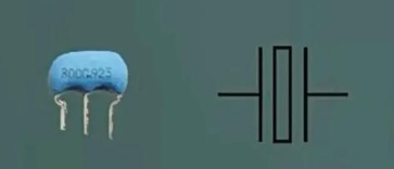
    Crystal oscillators provide clock signals in many circuits that require precise and stable timing. By physically oscillating piezoelectric materials (such as crystals), they generate periodic electronic signals, hence their name. Each crystal oscillator is designed to vibrate at a specific frequency, which is more stable, economical, and smaller in size than other timing methods. That’s why they are commonly used for precise timing in microcontrollers, or more commonly as clock components in quartz watches.

    10. Switches and relays

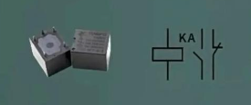
    A basic and easily overlooked component, a switch is simply a power button that controls the current in a circuit by switching between open or closed circuits. They vary greatly in appearance, from sliders, rotations, buttons, levers, toggles, key switches, and more. Similarly, a relay is an electromagnetic switch that operates through a solenoid, acting like a temporary magnet when a current flows through it. They act as switches and amplify small currents into larger ones.

    Now that you’re familiar with some basic electronic components, why not dive into creating your own electronics project? Instead of starting with a complex project featuring advanced functions, begin with a few simple ones. As with any hobby, you’ll encounter challenges along the way, but these hurdles are not insurmountable. With accessible and affordable beginner electronics tools like Arduino and CAD tools, the maker community welcomes new PCB designs and projects every day.

    In addition to PCB manufacturing, EBest Circuit (Best Technology) offers a full turnkey service, including parts procurement and assembly. Whether you’re working on prototypes or scaling up to mass production, Best Team provides a one-stop solution for seamless and hassle-free PCB assembly.

    You may also like

    PCB vs CCA: What is a Circuit Card Assembly?
    Monday, July 22nd, 2024

    Hey there! If you’re curious about circuit card assembly (CCAs) and what makes them tick, you’ve come to the right place. CCAs are the unsung heroes behind many of the electronic devices we use every day. Let’s dive into what they are, their essential parts, how they’re made, and why they’re so important.

    What is a circuit card assembly?

    Circuit card assembly or CCA is the process of producing printed circuit boards. In essence, it is the same as PCBA (PCB assembly), just in different name. CCA is a manufacturing technology that converts raw materials into printed circuit boards. It is used in many industries, including the military and aerospace sectors. This type of manufacturing requires skilled professionals to lay out the design and then assemble it. If you are planning to buy a batch of circuit card components, here are some things you should know about CCA.

    PCB vs CCA: What is a Circuit Card Assembly?

    A circuit card is a thin, flat dielectric material on which conductive paths or traces are etched. These paths connect various electronic components. They are also used to connect components to sockets on printed circuit boards. Circuit card assy is the process of manufacturing circuit card components. The process involves adding electronic components to the substrate.

    Key components of a circuit card assembly (CCA)

    Circuit card assembly have several key components to make the circuit function properly. These can be divided into three basic components.

    • Printed Circuit Board (PCB)
    • Electronic component
    • Solder paste
    • Printed Circuit Board (PCB)

    This is the backbone of the CCA. The printed circuit board provides the structural foundation on which all other components are mounted. A PCB is typically made of a flat, insulating material such as FR4 fiberglass, which is layered with conductive tracks made of copper. These tracks form the circuit pathways that connect various electronic components. The PCB board can be single-sided, with components and conductive tracks on one side only, or double-sided, with tracks and components on both sides. For more complex applications, multi-layer PCBs are used, which consist of multiple layers of insulating material and conductive pathways stacked together. These printed circuit boards are essential in ensuring that electrical signals are routed efficiently and reliably across the assembly.

    PCB vs CCA: What is a Circuit Card Assembly?

    • Electronic Components

    These include resistors, capacitors, integrated circuits, transistors, and more passive and positive components. Each part plays a specific role in the circuit, like pieces of a puzzle fitting together to make a complete picture. Resistors control the flow of electrical current, capacitors store and release energy, integrated circuits (ICs) perform various functions like processing and memory storage, and transistors act as switches or amplifiers. These components are carefully placed on the PCB in positions that allow them to connect and interact as designed.

    PCB vs CCA: What is a Circuit Card Assembly?

    • Solder paste

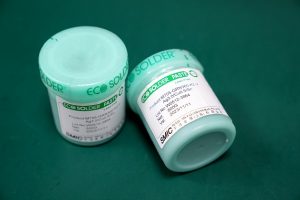
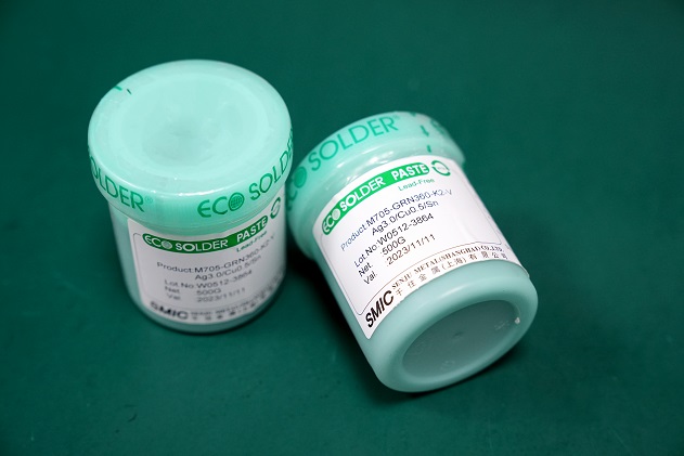
    Solder paste is like the glue that holds everything together, but it’s electrically conductive. It’s used to attach the electronic components to the PCB, so that they can stay put and work properly. Soldering creates a strong, conductive bond between the component leads and the PCB’s copper tracks. There are different types of soldering, such as lead-based and lead-free solders, each with its specific properties and applications. The soldering process can be done manually or using automated printing machines, depending on the complexity and volume of the assembly. Please noticed that solder paste should used in a very short time, otherwise, it will become dry solder paste.

    PCB vs CCA: What is a Circuit Card Assembly?

    What is the Difference Between a PCB and a CCA?

    You might wonder, what’s the difference between a PCB and a CCA? Well, here’s a quick rundown:

    AspectPCB (Printed Circuit Board)CCA (Circuit Card Assembly)
    DefinitionA blank board with conductive pathwaysA PCB populated with electronic components
    ComponentsNo electronic componentsIncludes electronic components like resistors, capacitors, ICs
    FunctionalityServes as the foundation for electronic circuitsA functional electronic circuit ready for use in devices
    Manufacturing StepsInvolves design, etching, and printing of conductive pathsInvolves PCB manufacturing plus component placement and soldering
    Usage StageIntermediate stage in manufacturingFinal stage, ready for integration into electronic devices
    ComplexityLess complex, involves fewer manufacturing stepsMore complex, involves multiple stages of assembly and testing

    What is the circuit card assembly manufacturing process?

    Making a CCA is a multi-step process:

    Design

    First, the PCB layout is designed using computer software. It includes numerous steps, like schematic drawing, layout design, SI, PI analysis, DFM. This can ensure the PCB board can fit all the necessary components and function correctly.

    Fabrication

    The PCB is then fabricated, which involves creating the physical board with layers of insulating and conductive materials. This is where the board gets its pathways. In this step, proceed strict quality control process to make sure the bare boards are qualified.

    Component Placement

    Next, printing solder paste and preparing components, then place them onto the PCB board according to the BOM file (bill of material). After setting up the pick and place machine, automated machines can precisely position each component based on the design.

    Soldering

    The components are soldered to the PCB. This can be done using methods like wave soldering or reflow soldering to ensure everything is securely attached and electrically connected. You must know, different products require different parameters, please make sure all the parameters like temperatures, time are suitable.

    Inspection and Testing

    The assembled CCA goes through rigorous inspection and testing to ensure it works as intended. This includes visual inspections, automated optical inspections (AOI), in-circuit testing (ICT), aging testing and functional testing.

    Final Assembly

    If the CCA passes all tests, it moves on to final assembly, where it’s integrated into the larger electronic system or device. That is we say the box building assembly.

    What are the types of circuit card assembly?

    CCAs can be divided into various types according to the different manufacturing technology.

    Through-Hole Technology (THT) Assembly

    Here, components have leads or pins inserted into holes drilled through the PCB and soldered on the other side. This method provides strong mechanical bonds, making it great for components that experience mechanical stress. It’s often used in aerospace, military, and industrial equipment.

    Surface Mount Technology (SMT) Assembly

    In SMT, components are mounted directly onto the PCB surface using solder paste. No drilling required, which allows for higher component density and smaller PCBs. This method is commonly used in consumer electronics, telecommunications, and automotive industries.

    Box Building Assembly

    Box building assembly involves the complete assembly of electronic systems, including CCAs, into enclosures or boxes. This process includes not only the assembly of the PCB but also the integration of cables, connectors, and other components into a final product. Box building is ideal for producing complete electronic devices ready for end-use.

    Advanced materials for CCAs

    Advanced materials help CCAs perform better and last longer:

    • High-Temperature Laminates (e.g., FR-4, Polyimide)

    High temperature laminate like FR4 or polyimide. These materials can handle extreme conditions without breaking down. FR-4 is popular for its excellent thermal and mechanical properties, while polyimide is great for high-temperature stability.

    • Flexible Substrates (e.g., Kapton, PET)

    Kapton and PET are the most common flexible substrate. These materials allow CCAs to bend and flex. Kapton, a type of polyimide, is known for its high thermal resistance and flexibility, making it perfect for wearable electronics and medical devices. PET (polyethylene terephthalate) is another flexible material with good electrical insulation properties.

    • Advanced Solder Compounds

    SAC305 (a lead-free alloy of tin, silver, and copper) is favored for its mechanical and thermal properties. Whatever you want to mount a ceramic PCB or the flexible PCB, it is the best choice. Sn63Pb37, a traditional tin-lead solder, is still used for its ease of use and excellent performance.

    Reliable circuit card assembly manufacturers

    Choosing the right manufacturer for your CCAs is key to getting quality products. PCBonline and EBest Circuit (Best Technology) are go-to-choice reliable circuit card assembly manufacturers. Both of them has advanced pick and place machine, full-auto SPI, AOI equipment, ensuring a good quality.

    As a leading manufacturer in the circuit card assembly, EBest Circuit (Best Technology) prides full turn-key service, ranging from the PCB design, PCB fabricating, electronic component sourcing, circuit card assembly and box build assembly. We handle complex and high-volume orders efficiently, ensuring timely and fast delivery without sacrificing quality. In 2023 alone, we completed over 5000 high-complexity projects with a client satisfaction rate of over 98%.

    It is crucial for anyone to fullly understand the circuit card assembly in the electronics industry. From their basic components and manufacturing process to the advanced materials used, CCAs are the backbone of modern electronic devices.

    You may also like