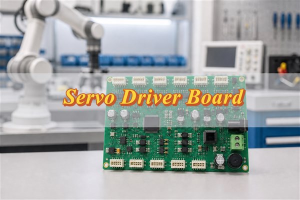
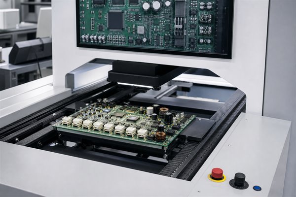
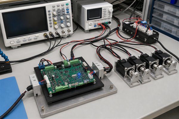
PCB manufacturing PCB manufacturing
Home > Blog

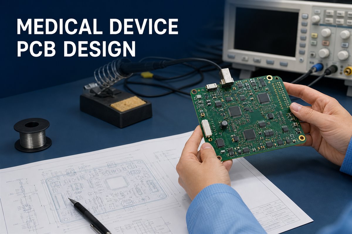
Medical Device PCB Design: Reduce Manufacturing Risk

August 14th, 2026

A medical device PCB design may work on the bench but still lose weeks in production because of mismatched revisions, unavailable parts, inaccessible test points, or unclear acceptance criteria.

Avoid those delays by releasing one buildable PCB/PCBA package before purchasing or tooling begins.

To simplify this handoff, EBest Circuit (Best Technology) gives you one sales contact backed by a three-person technical team for DFM, PCB fabrication, sourcing, assembly, inspection, and agreed testing.

medical device pcb design

What Medical Device PCB Design Must Define Before Manufacturing

Get an accurate quotation and prevent revision mistakes by sending one approved manufacturing package.

Include:

  • Gerber or approved ODB++/IPC-2581 data, drill files, and route data
  • fabrication drawing, stackup, impedance requirements, materials, finish, and tolerances
  • approved BOM with manufacturer part numbers and substitution rules
  • centroid data and assembly drawings with polarity, variants, and do-not-fit parts
  • programming, inspection, and test requirements with pass/fail criteria
  • one consistent revision across all files

If the fabrication drawing says revision B while the BOM says revision C, production should stop for clarification. Resolving that conflict before material purchase costs less than rebuilding an assembled batch.

EBest provides a DFM report showing the affected feature, manufacturing risk, recommended action, and required approval.

PCB Design Methods That Reduce Manufacturing Risk

Protect the next production lot by checking whether the layout fits a stable manufacturing and inspection process—not merely whether it passes CAD rules.

Before layout release, confirm:

  • trace, spacing, drill, annular ring, solder-mask, and copper-to-edge capability
  • stackup availability and controlled-impedance compatibility
  • component spacing, thermal pads, fiducials, tooling clearance, and depaneling method
  • access for AOI, X-ray, flying probe, ICT, or functional testing
  • whether HDI, via-in-pad, flex, or rigid-flex features are technically necessary

EBest’s experienced PCB/PCBA engineers identify process-fit problems before tooling, when changes cost less.

Material Selection for Reliable Medical PCBs

Avoid emergency substitutions by confirming material availability and approval rules before the build.

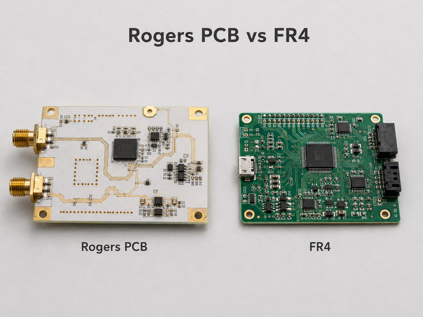
“FR-4” alone does not define laminate performance. Impedance, dimensional stability, assembly heat exposure, and future availability can depend on the exact laminate and construction.

Confirm in writing:

  • whether the exact laminate is mandatory or an approved equivalent is allowed
  • which dielectric values and thicknesses control impedance
  • operating conditions and assembly heat-cycle requirements
  • required material certificates, declarations, date codes, and lot records
  • who can approve a substitute and how approval will be recorded

EBest provides a BOM optimization list covering availability, lifecycle, package, and alternative-part risks before purchasing. EBest works with 1,000+ supply-chain partners; you retain approval of electrical equivalence and design changes.

How Medical Device PCB Assembly Changes the Design Review

Reduce handoff errors by reviewing the PCB, BOM, assembly data, and test requirements as one release.

Once components are added, the review must also cover land patterns, polarity, paste apertures, component height, moisture sensitivity, programming, inspection, and test limits.

EBest coordinates PCB fabrication, component sourcing, assembly, and agreed testing through one team.

A release-ready assembly package should define:

  • approved parts and substitution rules
  • polarity, variants, and do-not-fit components
  • solder alloy, paste, and relevant thermal constraints
  • programming files and verification requirements
  • inspection coverage and acceptance criteria
  • test method, fixture, software version, and pass/fail responsibility

EBest supports samples and small batches, helping you verify manufacturing, assembly, and testing before scaling.

When files, materials, test scope, and capacity permit, EBest can deliver PCBAs in approximately 1.5 weeks. Confirm the project-specific schedule in the quotation.
DFM Checks Before Prototype Release

Release prototypes with fewer open questions by requesting a DFM report that leads to decisions.

The review should cover:

  • stackup, thickness, copper weight, impedance, and drawing consistency
  • trace, spacing, drill, annular ring, mask dam, and edge clearance
  • via treatment, copper balance, panelization, tooling, and fiducials
  • footprint-to-BOM consistency, polarity, clearance, and paste apertures
  • test-point access and fixture constraints
  • revision alignment across every production file

Separate release blockers, customer approvals, and optional improvements affecting cost, yield, or lead time. Link every approved deviation to the applicable revision.

EBest’s experienced R&D and PCB/PCBA engineers provide practical process recommendations—not unexplained factory questions.

medical device pcb design

Inspection and Reliability Testing Evidence to Request

Make test results usable by defining what will be checked, against which limit, and what record you will receive. “100% tested” is not enough without a method and acceptance criteria.

Match each risk to evidence:

  • material identity: manufacturer, lot, date-code, and incoming records
  • bare-board opens and shorts: electrical or flying-probe results
  • hidden solder joints: X-ray records where required
  • placement and polarity: first-article and AOI records
  • controlled characteristics: specified impedance, microsection, cleanliness, or solderability reports
  • product function: customer-defined method, fixture, software, and pass/fail limits
  • investigation: serial number, work order, traveler, nonconformance, and corrective-action records

EBest’s ISO 13485:2016-certified quality system supports controlled revisions, suppliers, records, traceability, and nonconformances. ISO 9001, IATF 16949, and AS9100D qualifications are also listed. These certifications do not replace final device certification.

Our digital workshop can trace material and product batches, production cycles, and progress in as little as five seconds, according to company-provided capability data.

medical device pcb design

A Medical Device PCB Design Example for Release Control

Suppose a monitoring-board project is moving from successful samples to a 100-unit pilot build. The PCB files are revision B, the BOM is revision C, two parts have long lead times, one diode has no polarity note, and “functional test” has no limits.

Starting immediately risks assembling the wrong revision, using an unapproved substitute, placing the diode incorrectly, and producing test results that cannot be repeated.

A safer release path is:

  1. Align all files under one approved revision.
  2. Record the revision, polarity, and test gaps in the DFM report.
  3. Provide BOM alternatives for customer approval before purchasing.
  4. Confirm panel, assembly, inspection, and test responsibilities.
  5. Build the pilot lot with the agreed production and traceability records.
  6. Return build feedback before the next quantity increase.

Move from a working prototype to repeatable pilot production with approved files, parts, tests, and records.

What to Include in a Medical PCB Manufacturing RFQ

Compare suppliers on the same scope by sending a decision-ready RFQ.

Include:

  • prototype, pilot, and expected production quantities
  • one revision-aligned PCB/PCBA release package
  • material, stackup, finish, tolerance, workmanship, and panel requirements
  • sourcing, substitution, and consigned-material rules
  • programming, inspection, testing, documentation, and retention requirements
  • packaging, labeling, traceability, and target delivery date

Ask suppliers to list assumptions, open questions, material risks, tooling charges, and lead-time conditions. This makes quotations easier to compare.

EBest combines 20 years of PCBA experience with in-house PCB and PCBA factories. The company reports serving 10,000+ engineers and 1,800+ customers.

Send controlled files, quantities, and evidence requirements to sales@bestpcbs.com. Receive DFM questions, sourcing risks, process recommendations, and a project-specific delivery plan before release.

FAQs About Medical Device PCB Design

What should I receive from a DFM review?

A written report showing the affected feature, manufacturing risk, proposed action, and required approval.

How does ISO 13485 help a medical PCB/PCBA buyer?

It supports controlled processes, records, suppliers, traceability, and nonconformance handling. It does not certify the finished medical device.

When should BOM availability be reviewed?

Check critical parts before layout freeze and review the approved BOM again before material release.

Can EBest support prototypes before volume production?

Yes. EBest supports samples and small batches so engineers can validate manufacturing, assembly, inspection, and testing before scaling.

What should I send for an accurate medical PCBA quotation?

For an accurate medical device PCB design quotation, send aligned PCB and assembly files, the approved BOM, quantities, material requirements, substitution rules, inspection and test scope, traceability needs, and target delivery date to sales@bestpcbs.com.

You may also like

Custom Servo Driver Board Manufacturing and PCB Assembly for AI Robot Hardware

August 14th, 2026

A servo driver board turns an AI robot controller’s motion commands into stable, synchronized actuator movement. A reliable custom design must match the servo interface, simultaneous current demand, control timing, connector system, PCB layout and test strategy; a simple bank of headers is not enough.

The scope covers PWM and serial-bus servo interfaces for robot hardware. Industrial AC servo drives require a separate motor-specific power-stage and control design.

Servo driver board for multi-axis AI robot hardware on a laboratory workbench

What Is a Servo Driver Board in AI Robot Hardware?

A servo driver board connects the robot processor, power source and servo actuators. Its exact role depends on the actuator and command architecture.

Its core functions are to distribute power, route or generate control signals, monitor required feedback and provide the necessary protection and connectors.

This interface must control timing, supply stability, contact reliability and logic integrity. The robot processor cannot correct these board-level failures after they occur.

How Does a Servo Driver Board Control Robot Motion?

The board converts a position, velocity or torque request into the electrical command format expected by each actuator. For a PWM servo, command timing encodes the requested position. For an addressed serial servo, a data packet identifies the actuator and target. Closed-loop industrial drives add current and feedback processing, so they require a different power and control architecture.

Evaluate the complete path under coordinated load; a single unloaded servo will not expose bus timing errors, voltage sag or corrupted feedback.

  • Deterministic updates: Schedule channel updates so simultaneous joints do not receive stale or irregular commands.
  • Safe startup: Hold outputs in a defined state until power rails, firmware and communication are ready.
  • Fault containment: Prevent one shorted cable or failed actuator from disabling unrelated control electronics when required by the system safety analysis.
  • Feedback integrity: Keep encoder, current, temperature and status paths away from noisy power switching loops.

How Do You Choose a Servo Driver Board for a Multi-Axis AI Robot?

Choose the board architecture from the actuator interface, peak simultaneous load and required motion coordination. Channel count by itself is not enough. Two boards with the same number of outputs can behave very differently when several joints accelerate together, when cables are long, or when the robot must recover safely after a fault.

Document these seven inputs before selecting the circuit architecture or connector count:

  • Actuator compatibility: Record every servo part number, supply range, command protocol, logic level and pinout. Confirm the interface from the actuator datasheet and, where possible, a known-good signal capture; a connector match alone does not prove electrical compatibility.
  • Axis count and update timing: Define the installed channels, axes that move together, required update period and worst-case bus latency. A board with enough outputs can still produce visible jitter if commands are delayed or updated unevenly.
  • Simultaneous power demand: Base the input rail, branch distribution and connector current rating on the real acceleration, reversal and holding profile. Normal running current can hide the short peaks that cause brownouts, resets or overheated contacts.
  • Feedback and diagnostics: Specify whether the controller needs position, current, temperature, status or fault data from each actuator. Confirm the required bandwidth and response to missing or invalid feedback before choosing a one-way PWM or bidirectional bus architecture.
  • Cable and connector limits: Control the mating part, pin sequence, wire gauge, cable length, retention method and mating-cycle requirement. These details affect voltage drop, signal integrity, serviceability and resistance to intermittent contact.
  • Startup and fault behavior: Define the output state during power-up, reset, undervoltage, overcurrent, watchdog timeout and communication loss. Decide whether one failed actuator or cable must remain isolated from the controller and other axes.
  • Mechanical and test integration: Check board outline, mounting, enclosure airflow, connector access, programming method and test-point access. Verify measurement and service access in the installed robot, because bench access may hide enclosure constraints.

Why Do Multiple Servos Jitter or Reset the Robot Controller?

Multi-servo jitter and controller resets usually begin with supply droop, shared return impedance, irregular command timing or EMI coupling. Diagnose these causes at the board while reproducing the loaded motion, not by replacing firmware or adding capacitors at random.

  • Reproduce the event: Run the exact joint combination, acceleration and mechanical load that causes the fault.
  • Measure at the load: Capture minimum rail voltage and transient duration at local connectors or test points with adequate bandwidth.
  • Correlate timing: Capture supply voltage, reset, command signal and fault output on the same time base.
  • Separate causes: Repeat with one actuator at a time, reduced acceleration and an alternate cable route to distinguish load current from coupling.
  • Verify the repair: Re-run the worst-case motion across the intended input-voltage and temperature conditions.

Also inspect shared connector pins, thin ground traces and long harness returns; transient current through these impedances can shift the local logic reference and trigger a reset.

How Should Power Integrity Be Designed for a Multi-Servo Driver Board?

Size and verify every element from the power source to the servo connector and return path under simultaneous motion. Use the real motion profile rather than channel count alone.

  • Model simultaneous current: Add the servos that can operate together, controller current and design margin; use stall current only for a credible operating or fault state.
  • Budget voltage drop: Calculate each source, protection, connector, copper, via, cable and return segment with Vdrop = I × R, then measure at the loaded connector.
  • Bulk energy: Place appropriately rated bulk capacitance where the servo rail enters and where a branch experiences a fast load step.
  • Local decoupling: Use the values specified by each controller, transceiver and power-device manufacturer, with short connections to the relevant supply and return pins.
  • Low-impedance distribution: Use copper geometry, layer transitions and connector contacts that match the calculated current and allowable temperature rise.
  • Rail separation: Keep noisy actuator current from flowing through the logic regulator’s sensitive supply and return path.
  • Protection coordination: Select reverse-polarity, surge, overcurrent and branch protection for the available source energy and credible harness faults.
  • Copper and stackup: Select FR4 copper weight and distribution from current, temperature rise, voltage drop and routing density; confirm spacing, vias, escape routing and manufacturability.

How Do PCB Layout, EMI and Thermal Design Affect Servo Board Reliability?

Coordinate switching-loop geometry, return paths, noise control and heat flow during PCB layout. One filter cannot correct poor routing after the layout is complete.

  • Shrink critical loops: Keep the source, switching device, load path, decoupling capacitor and return loop compact.
  • Preserve return paths: Avoid routing that cuts the reference plane beneath clocks, buses and sensitive measurements.
  • Partition by function: Separate power switching, logic, analog sensing and external interfaces while providing deliberate connection points between their returns.
  • Control coupling: Increase separation from noisy nodes, reduce long parallel runs and protect high-impedance signals.
  • Build a thermal path: Connect exposed pads to continuous copper and an appropriate thermal-via pattern, then measure the assembled board under the worst credible motion profile.
  • Record thermal conditions: Log input voltage, active channels, mechanical load, airflow, enclosure state, ambient temperature and soak time with every temperature result.

Compare component and board hot spots with the applicable device limits, derating policy and robot duty cycle.

How Does a Custom Servo Driver Board Prototype Validate Robot Performance?

Validate the prototype under representative multi-axis load; one unloaded servo is not sufficient release evidence. Use six verification gates:

  1. Design for observation: Add safe access to input, servo and logic rails, ground, reset, communication, command outputs and current measurement.
  2. Verify static safety: Check shorts, polarity and rail resistance, then perform the first power-up with a current-limited supply before connecting actuators.
  3. Validate one channel: Confirm signal format, connector pinout, direction, range and fault behavior with one known actuator.
  4. Increase concurrency: Add channels according to the real robot motion profile while logging minimum rail voltage, current and timing.
  5. Apply mechanical load: Test acceleration, reversal, holding and collision-recovery states that change actuator current.
  6. Record release evidence: Save waveforms, temperatures, firmware version, board revision, actuator list and pass limits.

What Must Be Controlled During Servo Driver Board PCB Assembly?

Assembly control must protect component identity, polarity, solder quality, connector alignment and thermal-pad integrity. Servo boards often combine fine-pitch logic, large capacitors, power packages and mechanically loaded connectors, so one uniform inspection method is insufficient.

Servo driver board PCB assembly undergoing automated optical inspection
  • BOM control: Lock manufacturer part numbers, approved alternates, package, ratings and do-not-substitute items.
  • Moisture handling: Follow the component and packaging requirements for moisture-sensitive devices before reflow.
  • Paste and reflow control: Match stencil apertures and the validated thermal profile to the component mix and exposed pads.
  • Polarity inspection: Verify diodes, electrolytic capacitors, IC orientation and connector pin-one features against controlled drawings.
  • Joint inspection: Use AOI for visible placement and solder features, then add X-ray where hidden joints or thermal pads create a real risk.
  • Connector mechanics: Check coplanarity, retention, insertion clearance and any hand-soldered or press-fit operation before functional test.
  • Revision control: Release matching fabrication, BOM, centroid and assembly files under one revision identifier.
  • Programming control: Define the image, checksum, security state, connector, fixture and pass record before assembly release.

Which Functional Tests Should Validate an AI Robot Servo Control Board?

Functional testing should verify power, every channel, communication, protection and loaded motion behavior against written limits. A power-on LED is only an initial observation; it does not prove channel timing, voltage margin or fault recovery.

AI robot servo control board functional testing with multiple servo actuators
Test Method
Input and rails Measure startup, steady state and worst-case transient at defined test points
All output channels Exercise each connector with a known load or validated simulator
Communication Test valid frames, timeout, missing device and bus recovery
Protection Apply controlled undervoltage, overload or disconnected-load conditions where safe
Loaded motion Run representative concurrent trajectories and mechanical loads
Programming and identity Read firmware, configuration, serial-number or revision identifiers

Set limits from actuator data, the control budget, safety analysis and system requirements. Use a protected fixture or simulator for unsafe fault tests and document its coverage limits.

How Do You Move a Servo Driver Board from Prototype to Production?

Release the design only after the board definition, approved parts, assembly controls and measurable acceptance limits are ready for repeat production. Confirm all eight requirements:

  1. Close prototype findings: Assign every electrical, thermal, communication and mechanical failure a root cause, corrective action and passing retest. Update the schematic, layout, BOM and firmware together so the released files match the tested board.
  2. Complete PCB DFM: Review the approved stackup, copper distribution, minimum geometry, drill and via structure, board outline, connector clearances, panelization and fabrication notes against the chosen manufacturer’s documented capabilities.
  3. Complete assembly and test DFM: Confirm package footprints, polarity marks, stencil requirements, fiducials, tool clearance, programming access and test-point size and spacing. The fixture must reach every required rail, interface and output without stressing connectors.
  4. Qualify the production BOM: Lock manufacturer part numbers for controllers, power devices, capacitors and connectors. Evaluate an alternate for electrical rating, pinout, package, thermal behavior, startup behavior and firmware compatibility before approval.
  5. Freeze production inputs: Issue matching Gerber or ODB++, drill, stackup, fabrication notes, BOM, centroid, assembly drawings, firmware image, programming instructions and functional-test specification under one revision.
  6. Build a production-intent pilot: Use the planned PCB construction, approved components, stencil, reflow process, programming method and test fixture. Temporary prototype wiring, hand-selected parts or laboratory-only setup must not hide transfer risks.
  7. Review pilot results: Classify fabrication, placement, soldering, programming and functional-test failures. Record rework and retest results, then verify rail voltage, timing, temperature and loaded multi-axis behavior against written limits before increasing quantity.
  8. Control post-release changes: Link every component, PCB, process, firmware or fixture change to an approval record and an affected-test plan. Repeat only the tests justified by the impact analysis, but never accept generic replacement equivalence without verification.

Why Choose EBest for Custom Servo Driver Board Manufacturing?

Reduce engineering handoffs, identify production risks earlier and keep the approved board and BOM aligned from prototype through repeat builds. These EBest Circuit services address those needs:

  • Resolve board-level risks before ordering volume: PCB design support can review power distribution, stackup, routing, connector placement and test access against the servo interface and motion-load requirements.
  • Validate the design with lower commitment: PCB prototyping and assembly services enable verification builds before the design moves to mass production.
  • Reduce uncontrolled BOM changes: Component sourcing and PCB assembly can work from the same approved manufacturer part numbers and flag alternatives that require engineering confirmation.
  • Match the PCB construction to the electrical load: EBest’s product scope includes FR4, multilayer, heavy-copper, high-Tg and impedance-controlled PCBs for project-specific stackup review.
  • Simplify prototype-to-production transfer: PCB design, prototype, sourcing, assembly and mass-production services can use one controlled set of fabrication, BOM, programming and test files.
  • Support supplier qualification: Use a defined PCB assembly manufacturer selection process to confirm sourcing responsibility, inspection, testing, traceability and change control. EBest lists IATF 16949, ISO 9001:2015, ISO 13485:2016, AS9100D, REACH, RoHS and UL credentials; confirm the certification and product-level documentation required for the specific robot program during quotation.
FAQs About Servo Driver Boards

Q1: What files should I send for a custom servo driver board quotation?

A1: Send the complete fabrication and assembly package. Include Gerber or ODB++, drill files, BOM, centroid data, assembly drawings, quantity, stackup, servo models, protocol, voltage, simultaneous-motion requirement, firmware method and functional test limits.

Q2: Can EBest assemble a customer-designed servo control PCB?

A2: Yes, EBest can fabricate and assemble a customer-designed board. The files still need engineering review for manufacturability, component availability and test readiness before release.

Q3: Can firmware be programmed during PCB assembly?

A3: Programming can be included with controlled inputs. Provide the firmware image, programming interface, security instructions and verification method, including the checksum or version readback that proves the correct image was loaded.

Q4: Does EBest provide a free DFM review before quotation?

A4: Yes, EBest offers a free DFM review for the submitted PCB and assembly package. The review can identify manufacturability issues involving stackup, copper geometry, drill and via choices, component footprints, assembly clearances and test access before production.

Q5: Which PCB constructions can be reviewed for a servo driver board?

A5: The appropriate construction depends on current, thermal, signal and mechanical requirements. EBest’s product scope includes FR4, multilayer, heavy-copper, high-Tg and impedance-controlled PCBs for project-specific review.

Q6: Can EBest support both bare PCB fabrication and complete PCB assembly?

A6: Yes, the service scope includes PCB fabrication, component sourcing and PCB assembly. Define whether the quotation requires bare boards, assembled boards, programming, functional testing or a combination of these services.

Q7: Which quality or compliance credentials should buyers confirm?

A7: Match the required certification or compliance document to the product and end-use program. EBest lists IATF 16949, ISO 9001:2015, ISO 13485:2016, AS9100D, REACH, RoHS and UL credentials; request the applicable current documentation during supplier qualification.

Q8: When is conformal coating appropriate for a robot servo board?

A8: Use conformal coating only when the environmental risk justifies it. Specify keep-out areas, connectors, test points and rework requirements; coating cannot compensate for inadequate spacing or enclosure design.

Q9: What information helps EBest provide a useful DFM review?

A9: Submit the manufacturing files together with the application’s electrical limits. Include Gerber or ODB++, stackup, BOM, centroid data, assembly drawings, servo models, voltage, simultaneous-load profile, connector constraints and required tests.

Q10: What records can accompany a servo driver board shipment?

A10: Define shipment records in the purchase specification. Request the inspection, programming, functional-test and traceability records needed for receiving acceptance before the order is released.

Conclusion

Ready to reduce manufacturing risk before ordering your servo driver board? Send your Gerber or ODB++, BOM, quantity, stackup, servo interface, simultaneous-load profile, assembly, programming and test requirements to sales@bestpcbs.com. Ask EBest for a free DFM review and quotation for your AI robot hardware project.

You may also like

Quarter-Wave Monopole vs Half-Wave Antenna: Which One Fits Your RF Design?

August 6th, 2026

A quarter-wave monopole uses a conductive ground plane as the electrical image of its missing second half. A center-fed half-wave dipole contains both radiating arms, so it can operate without using the product chassis or PCB ground as its return structure.

Neither is universally better. The monopole is shorter and easy to integrate into a grounded product. The dipole occupies more space but is less dependent on RF PCB ground quality. The right choice follows from enclosure size, frequency, mounting, polarization, matching, and the final operating environment.

Quarter-wave monopole antenna compared with a half-wave dipole antenna

What Does Quarter-Wave Monopole vs Half-Wave Actually Compare?

The useful comparison is a quarter-wave monopole against a center-fed half-wave dipole. They can produce similar radiation behavior, but create the required RF current path differently.

  • Quarter-wave monopole: one conductor about one-quarter wavelength long, positioned above or beside an RF ground.
  • Half-wave dipole: two conductors, each about one-quarter wavelength long, fed between their inner ends.
  • Half-wave monopole: a different end-fed structure with high feed-point impedance; it is not another name for a dipole.

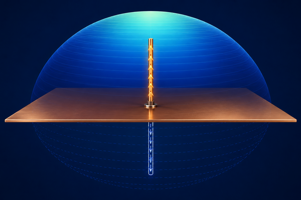
In the ideal monopole model, the conductive plane creates an electromagnetic image of the visible element. The element and its image behave much like the two arms of a dipole. The ground plane is therefore an active part of the antenna, not spare copper.

How Is Antenna Length Calculated?

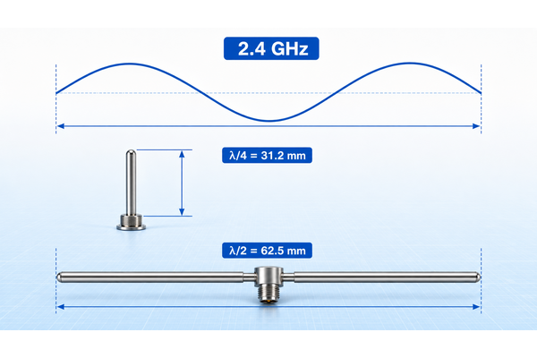
Free-space wavelength is λ = c/f, where c is approximately 299,792,458 m/s and f is frequency in hertz. Initial dimensions are c/(4f) for a quarter-wave element and c/(2f) for a half-wave dipole overall.

Quarter-wave and half-wave antenna length at 2.4 GHz
FrequencyWavelengthQuarter waveHalf wave
433 MHz692.4 mm173.1 mm346.2 mm
868 MHz345.4 mm86.4 mm172.7 mm
915 MHz327.6 mm81.9 mm163.8 mm
2.4 GHz124.9 mm31.2 mm62.5 mm
5.8 GHz51.7 mm12.9 mm25.8 mm

These are starting values. Conductor width, substrate, solder mask, enclosure plastic, battery position, ground geometry, and the user’s hand shift resonance. For a printed antenna, do not shorten the trace using FR4 Dk alone: part of its field travels through air. Start from a proven reference layout and retain copper that can be trimmed during prototype tuning.

Quarter-Wave Monopole vs Half-Wave Dipole: Key Differences

ParameterQuarter-wave monopoleHalf-wave dipole
StructureOne λ/4 element plus RF groundTwo λ/4 arms
Overall radiatorAbout λ/4 visibleAbout λ/2
Ground planeRequired for intended operationNot required as a radiating arm
Ideal feed resistanceAbout 36.5 ΩAbout 73 Ω
FeedUsually unbalancedBalanced; coax normally needs balun/choke
Product sensitivityStrongly affected by ground/chassisLess dependent on product ground
Best fitGrounded embedded productsGround-independent external antennas

Why Does a Quarter-Wave Monopole Need a Ground Plane?

The ground plane provides the RF return-current path and the image current that lets a λ/4 element behave like half of a dipole. In a product, it may be continuous PCB copper, a vehicle roof, a metal chassis, radial wires, or a combination of PCB ground and conductive mechanical parts.

Quarter-wave monopole ground plane and electromagnetic image

A small or fragmented ground changes impedance, resonance, efficiency, and pattern. RF current may be forced onto USB cables, coax shields, harnesses, or the user’s body. Return loss can still look respectable even while useful radiated power is poor. A dipole supplies its own second arm, although nearby metal and an unbalanced cable can still disturb it.

How Do Impedance and Matching Differ?

Most radios, coax connectors, and PCB transmission lines use 50 Ω, so either antenna may need matching. Monopole impedance can be adjusted through element geometry, feed position, ground dimensions, and radial angle. A dipole’s nominal 73 Ω value also moves with conductor diameter, installation height, and nearby material.

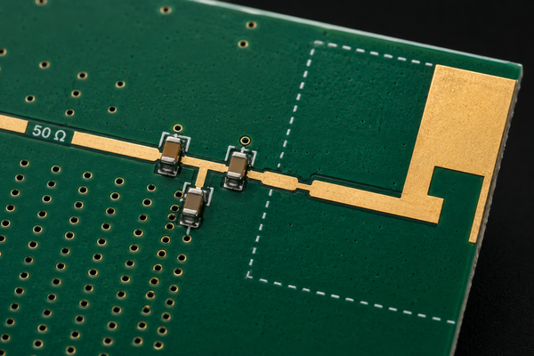
50 ohm PCB feed and pi matching network for a printed monopole antenna
  • Reserve a π-network footprint on embedded prototypes, even if the first build uses a zero-ohm link.
  • Use a balun or common-mode choke when coax feeds a balanced dipole.
  • Measure in the final mechanical assembly before locking values.
  • Do not treat matching as a cure for a lossy radiator or inadequate ground.

A low VSWR only confirms limited reflected power at the feed. It does not prove good radiation efficiency or range.

Which Antenna Has More Gain and Range?

A free-space half-wave dipole has about 2.15 dBi theoretical maximum directivity. An ideal quarter-wave monopole over an infinite perfect ground can reach about 5.15 dBi because energy is confined to one hemisphere. That 3 dB difference should not be applied blindly to compact products.

Realized range depends on transmit power, realized gain in the required direction, efficiency, receiver sensitivity, polarization, matching and feed losses, mounting height, obstacles, and multipath. With a useful ground plane, a monopole is compact and effective. With a small or unpredictable ground, a properly fed dipole may be more repeatable.

How Do Radiation Pattern and Polarization Compare?

Both can give broadly omnidirectional azimuth coverage when vertical and kept clear of conductors. Their weakest directions are along the antenna axis. Installation often changes the pattern more than the ideal antenna type.

  • Vertical radiators produce vertical polarization; a tilted device introduces mismatch.
  • A horizontal dipole has nulls off its ends.
  • Batteries, displays, shields, motors, and metal housings can create deep nulls.
  • Uncontrolled feedline current makes the cable radiate and distorts measurements.

For handhelds, trackers, and sensors, review the three-dimensional pattern. Uniform coverage may matter more than a single peak-gain figure.

Which Antenna Is Better for PCB and Embedded RF Products?

A printed monopole is a sensible starting point when the PCB has adequate ground and the antenna can sit at a board edge. A dipole is attractive where product ground is limited or varies between host devices.

SituationStarting optionReason
2.4 GHz IoT device with adequate PCBPrinted monopole or IFALow BOM cost and direct integration
Very small sub-GHz PCBExternal dipole or validated loaded antennaλ/4 is long and ground may be inadequate
Metal enclosureExternal antennaThe enclosure can shield an internal radiator
Vehicle installationRoof-mounted monopoleThe roof provides a useful ground plane
Ground-independent external antennaHalf-wave dipoleBoth radiating arms are included
Body-worn productPrototype and test bothBody loading detunes and absorbs RF

PCB Layout Rules for a Quarter-Wave Monopole

A printed monopole is an RF structure, not an ordinary trace. Copying only its outline while changing stack-up, ground size, feed geometry, or enclosure can produce a different antenna.

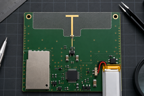
Printed quarter-wave monopole PCB layout with antenna keep-out
  • Place the radiator at the board edge and preserve the reference orientation.
  • Maintain the specified copper and component keep-out on every relevant layer.
  • Keep batteries, displays, shields, cables, screws, and housing metal away.
  • Route the feed as controlled 50 Ω microstrip or grounded coplanar waveguide.
  • Use continuous RF ground under the feed, but not under a keep-out radiator.
  • Add ground stitching vias at RF transitions and along grounded coplanar edges.
  • Keep the matching network close to the feed and leave room for tuning.
  • Add a conducted test connector or test path to early prototypes.

Common Antenna Failures and What They Really Mean

Observed problemLikely causeCheck
Resonance below targetElement too long or excess nearby capacitanceTrim the tip gradually in the final enclosure
Resonance above targetElement electrically shortAdd length or revise matching
Good S11, poor rangeLow efficiency or unintended cable/chassis lossMeasure OTA efficiency and packet performance
Performance changes when touchedHand loading and inadequate isolationTest realistic grip positions
Unit-to-unit range variationMaterial, assembly, housing, or matching spreadCompare multiple production samples
Dipole pattern distortedCommon-mode coax currentCorrect the balun or choke

Tune after the complete mechanical assembly exists. An exposed PCB tuned on a bench can shift once it is placed beside a battery, coated, and closed inside plastic.

How Should the Antenna Be Tuned and Tested?

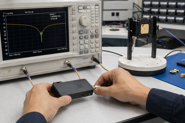
A vector network analyzer reveals feed impedance, return loss, and resonance. Over-the-air testing is still required to judge radiation performance.

RF engineer testing an embedded antenna with a vector network analyzer
  1. Begin with a validated reference layout and preserve its stack-up, feed, keep-out, and ground assumptions.
  2. Measure the bare PCB and record S11 and impedance.
  3. Add the battery, display, shields, cables, screws, coating, and enclosure.
  4. Measure after each assembly stage to identify the source of detuning.
  5. Adjust physical length in small increments before changing several network parts at once.
  6. Optimize matching with production-grade RF capacitors and inductors.
  7. Check RSSI, packet error rate, throughput, or sensitivity in several orientations.
  8. Test several units and complete regulatory verification in maximum transmit mode.

For range-critical or positioning products, total efficiency and 3D radiation-pattern measurements provide far more information than return loss alone.

What Should Be Checked Before PCB Production?

  • Operating bands, channels, and target bandwidth
  • Final laminate, thickness, copper weight, and stack-up
  • Controlled-impedance geometry and reference plane
  • Antenna dimensions and manufacturing tolerances
  • Keep-outs on every layer and solder-mask requirement
  • Matching footprint and available RF component values
  • Battery, shield, display, connector, and hardware locations
  • Prototype RF test connector and tuning plan
  • Enclosure material, spacing, and final-use orientation

Do not silently substitute laminate or board thickness after validation. Send the PCB manufacturer the approved stack-up, impedance requirement, antenna drawing, and keep-out notes together.

Frequently Asked Questions

Is a quarter-wave antenna better than a half-wave antenna?

Not universally. The monopole is compact when a good ground exists; the dipole is longer but less dependent on chassis ground.

Does a quarter-wave monopole have the same pattern as a half-wave dipole?

Over an infinite perfect ground, its upper-half pattern resembles a dipole. Finite ground changes the practical result.

Why does a quarter-wave monopole require a ground plane?

The plane supplies the RF return path and creates the electromagnetic image of the missing arm.

Can a quarter-wave antenna work without a ground plane?

It may radiate, but cables, PCB ground, or the enclosure become uncontrolled parts of the antenna.

Does a half-wave antenna need a ground plane?

A center-fed dipole does not, but a coax-fed version normally needs a balun or common-mode choke.

What is the impedance of a quarter-wave monopole?

About 36.5 Ω in the ideal model; real geometry and ground size can move it substantially.

What is the impedance of a half-wave dipole?

About 73 Ω for a thin free-space resonant dipole, with installation-dependent variation.
Is a monopole always half the length of a dipole?

Its visible element is about half the total dipole span, but its ground or counterpoise also occupies space and performs an electrical function.
How long is a quarter-wave antenna at 2.4 GHz?

The free-space value is about 31.2 mm; printed versions may be shorter after dielectric and enclosure loading.

How long is a quarter-wave antenna at 915 MHz?

About 81.9 mm in free space. Loading can reduce size at the cost of bandwidth or efficiency.

Does a longer antenna always provide more range?

No. Resonance, efficiency, impedance, orientation, and the full link budget determine range.

Can a PCB ground plane be too small?

Yes. It can reduce efficiency, shift resonance, distort coverage, and increase hand or cable sensitivity.

Why does an antenna fail inside its enclosure?

Plastic, adhesive, batteries, displays, shields, wiring, and fasteners change the electromagnetic environment.

Is VSWR enough to judge antenna quality?

No. It measures matching, not useful radiation. Evaluate efficiency and OTA performance too.
Should I use a monopole or dipole for a small IoT device?

Start with a proven printed monopole or IFA when adequate ground exists; consider a dipole or external antenna when ground is small or unpredictable.

Engineering Support for RF PCB Projects

The monopole is normally the smaller and lower-cost option, but ground, feedline, enclosure, and matching must work as one RF system. A dipole needs more span yet can be more predictable when reliable chassis ground is unavailable.

Before production, validate resonance, impedance, efficiency, coverage, enclosure effects, and unit-to-unit consistency. Lock the approved stack-up, controlled-impedance geometry, antenna keep-out, solder-mask requirement, and tuning provisions before Gerber release.

If you are sourcing PCB/PCBA manufacturing for prototyping, custom engineering, or volume production, contact the EBest engineering team at sales@bestpcbs.com.

You may also like

Aerospace PCB Fabrication Requirements Before Production

July 31st, 2026

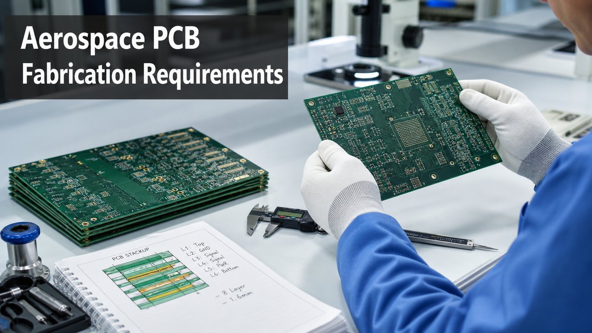
aerospace pcb fabrication requirements are the material, stackup, copper, drilling, surface finish, inspection, and documentation details that must be confirmed before an aerospace-related PCB moves into production. For avionics, satellite electronics, UAV modules, radar equipment, communication systems, power control units, and other high-reliability applications, a small missing note in the fabrication package can create cost changes, schedule delays, or assembly risk later.

For buyers and engineers, the goal is not only to find a PCB factory. The goal is to work with a supplier that can review manufacturability, material risk, process tolerance, documentation needs, and PCBA handoff before fabrication starts. EBest Circuit (Best Technology) supports PCB fabrication, DFM review, PCB layout manufacturability review, component sourcing, PCBA assembly, and testing support for prototype, small-batch, and production projects. For aerospace-related PCB or PCBA inquiries, you can contact sales@bestpcbs.com with Gerber files, stackup notes, BOM, assembly drawings, and test requirements.

aerospace pcb fabrication requirements
Aerospace PCB fabrication requirements should be reviewed before production to reduce material, stackup, and assembly risk.

What Are Aerospace PCB Fabrication Requirements?

Aerospace PCB fabrication requirements define how a board should be manufactured, inspected, documented, and prepared for later assembly. They are usually stricter than ordinary commercial PCB requirements because the board may face vibration, temperature change, humidity, mechanical stress, long service life, or difficult repair conditions.

In a normal consumer product, a buyer may focus mainly on price, lead time, layer count, and surface finish. In an aerospace PCB project, the discussion usually needs to go deeper:

  • Which laminate is specified, and is an approved equivalent allowed?
  • Is the stackup controlled by impedance, dielectric thickness, or overall board thickness?
  • What copper thickness and hole wall plating are needed?
  • Are microvias, buried vias, via-in-pad, or controlled-depth drilling involved?
  • Does the board need special cleanliness, solderability, or coating preparation?
  • What inspection records, test reports, or traceability documents are required?
  • Will the PCB fabrication choice create difficulty during PCBA assembly?

These requirements should be confirmed before quotation whenever possible. If they are only discussed after fabrication starts, the supplier may need to change materials, adjust tooling, add inspection steps, or revise the delivery schedule.

Material Requirements for Aerospace Printed Circuit Boards

Material choice is one of the first decisions for aerospace printed circuit boards. The material does not only affect price; it affects thermal stability, dimensional movement, signal behavior, drilling quality, moisture resistance, and long-term reliability.

Common material directions include:

Material direction Where it may fit Buyer should confirm
High-Tg FR4 Control boards and moderate thermal environments Tg, CTI, thickness, copper weight
Polyimide Higher temperature or flex/rigid-flex needs Flex cycle, bend area, adhesive system
RF laminate Radar, antenna, microwave, or communication designs Dk, Df, impedance, laminate availability
Ceramic PCB Heat dissipation or special thermal needs Ceramic type, metallization, assembly method
Metal core PCB Thermal management for power or LED-related modules Dielectric, thermal conductivity, isolation

The mistake buyers often make is treating “aerospace PCB material” as one fixed category. In real production, the right material depends on the function of the board. A low-speed controller, a radar RF board, a satellite power module, and a rigid-flex interconnect may all fall under aerospace-related electronics, but their fabrication requirements can be very different.

Before production, the RFQ package should make the material requirement clear:

  • Exact laminate brand and grade, if locked by the design.
  • Whether equivalent material can be reviewed.
  • Required board thickness and tolerance.
  • Copper weight for inner and outer layers.
  • Thermal, RF, or mechanical reasons behind the material choice.
  • Any certificate, traceability, or material report needed for the project file.

If the design allows material substitution, the supplier should not simply replace the laminate to reduce cost. The change should be reviewed against impedance, thermal behavior, drill quality, soldering temperature, and assembly reliability.

Key Manufacturing Requirements in Aerospace PCB Fabrication

Aerospace PCB fabrication should be discussed around risk control, not only board specifications. The same layer count and board size can produce very different manufacturing difficulty depending on copper balance, hole density, aspect ratio, impedance tolerance, material type, and inspection requirements.

aerospace pcb fabrication requirements
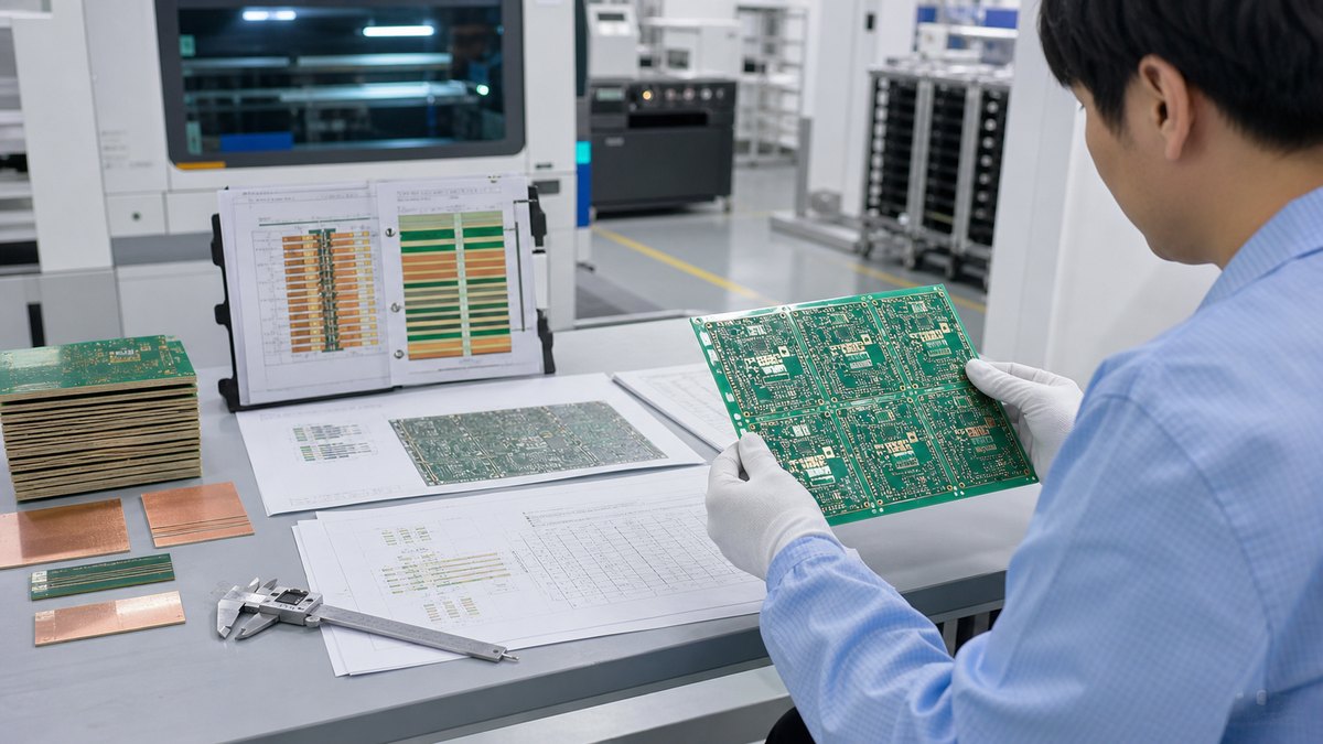
Manufacturing review for aerospace PCB fabrication should connect stackup, copper, drilling, surface finish, and DFM checks.

Important manufacturing requirements include:

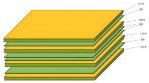
  • Stackup control: dielectric thickness, copper distribution, prepreg selection, and press cycle must support the electrical and mechanical target.
  • Copper and plating: copper weight, hole wall copper, plating uniformity, and annular ring control affect current carrying, soldering, and via reliability.
  • Drilling quality: small holes, dense vias, back drilling, blind vias, or buried vias need careful review before tooling.
  • Registration tolerance: multilayer aerospace PCBs need stable layer-to-layer alignment, especially with fine-pitch components or impedance traces.
  • Surface finish: ENIG, ENEPIG, immersion silver, hard gold, or other finishes should be selected based on soldering, wire bonding, contact wear, shelf life, and reliability needs.
  • Cleanliness and handling: ionic contamination, residue, scratches, and poor storage can create problems that do not appear during a quick visual check.

A useful supplier will review these points before production rather than waiting for the factory floor to discover conflicts. For example, a customer may specify thick copper for current capacity and fine BGA pitch for compact layout. Both needs may be valid, but the combination can affect etching tolerance, solder mask clearance, drill-to-copper spacing, and assembly yield. That is where DFM review becomes practical, not just procedural.

Reliability Requirements for High Reliability PCB for Aerospace

High reliability PCB for aerospace projects must be built around the product’s working environment. Reliability is not created by one certificate or one final test. It comes from correct material selection, stable fabrication control, clear inspection criteria, and practical assembly planning.

Typical reliability questions include:

  • Will the board face thermal cycling between low and high temperatures?
  • Is vibration or mechanical shock expected?
  • Are connectors, cables, BGAs, or heavy components exposed to mechanical stress?
  • Does the board need controlled impedance, low loss, or high-frequency performance?
  • Will the product be repaired, serviced, or sealed after assembly?
  • Does the customer require special inspection records or production traceability?

For high-reliability boards, the supplier should also pay attention to failure modes that are easy to overlook:

  • barrel cracking in plated through holes
  • resin recession or poor hole wall quality
  • laminate movement that changes impedance
  • solder mask clearance that affects assembly
  • BGA voiding or hidden solder joint risk
  • contamination that affects insulation resistance
  • connector stress caused by cable routing or housing design

This is why an aerospace-related PCB project should not be quoted only from board size and layer count. A professional quotation needs to understand where the board will be used, what the critical circuits are, which parts are difficult to assemble, and what inspection evidence the buyer needs after production.

Design File and DFM Checks Before Aerospace PCB Production

Before aerospace PCB production, the most valuable step is a practical file review. Many production problems are already visible in the Gerber, drill, stackup, BOM, CPL, and assembly drawing package before a single panel is made.

Key checks include:

  • Gerber and drill file consistency.
  • Stackup notes versus impedance requirements.
  • Minimum trace width and spacing.
  • Drill size, aspect ratio, annular ring, and hole-to-copper spacing.
  • Copper balance and high-current areas.
  • Controlled impedance trace width, reference plane, and dielectric thickness.
  • Solder mask clearance around fine-pitch pads.
  • Via-in-pad, plugged via, filled via, or capped via requirements.
  • Surface finish and assembly process compatibility.
  • Panelization, fiducials, tooling holes, and breakaway tabs.

For PCBA projects, the supplier should also compare PCB files with the BOM and placement file. A footprint that looks acceptable in Gerber may still create assembly risk if the component package, pin 1 orientation, thermal pad size, or connector direction is unclear.

EBest Circuit can support PCB layout manufacturability review and DFM analysis. That means checking whether the layout can be manufactured and assembled reliably, not taking over full aerospace electronic system design. This boundary matters because aerospace projects often involve customer-owned electrical design decisions, compliance requirements, and product-level validation that must remain under the customer’s engineering control.

PCBA Assembly Requirements After Aerospace PCB Fabrication

PCBA assembly requirements should be considered before PCB fabrication is released. If fabrication and assembly are treated as separate decisions, the board may be manufacturable but difficult to assemble, inspect, or test.

Important PCBA assembly requirements include:

  • Component package type: BGA, QFN, LGA, fine-pitch IC, connector, shield, or press-fit part.
  • Soldering process: SMT, through-hole, selective soldering, hand soldering, or mixed assembly.
  • Thermal profile: material, finish, copper area, and component sensitivity must match the reflow process.
  • Inspection access: AOI and X-ray requirements should be planned before layout and panelization are finalized.
  • Cleaning and coating: spacing, component height, connectors, and test points affect process choice.
  • Test strategy: flying probe, ICT, functional test, programming, and fixture planning may affect pad access and schedule.

For example, a rigid PCB for an aerospace sensor module may look simple from the fabrication side. But if it has fine-pitch connectors, a shield can, a thermal pad QFN, and test pads only on one crowded side, assembly yield and inspection confidence can become the real challenge. In that case, the better supplier response is not only “we can make the PCB.” It is to review solder paste opening, X-ray access, connector stress, reflow compatibility, and test point availability before production.

EBest Circuit supports turnkey PCB and PCBA service, including PCB manufacturing, component sourcing, SMT assembly, through-hole assembly, inspection, and testing support. For buyers, this reduces the risk of passing a board from one vendor to another without anyone checking the full manufacturing path.

Quality Standards and Traceability for Aerospace PCB Projects

Quality standards and traceability are central to aerospace PCB projects because buyers often need more than finished boards. They may need production records, inspection evidence, material information, and clear batch control.

aerospace pcb fabrication requirements
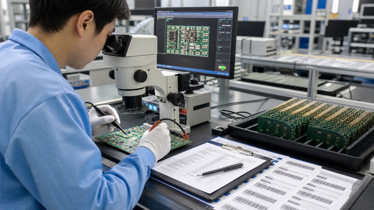
Inspection and traceability records help buyers confirm aerospace PCB quality before shipment.

Common quality and documentation topics include:

Requirement area What buyers may request
Quality system ISO 9001, AS9100D, or project-specific quality procedures
Fabrication inspection AOI, electrical test, microsection, solderability, dimensional check
Assembly inspection AOI, X-ray for BGA/QFN, visual inspection, first article review
Traceability material lot, production batch, process route, inspection record
Documentation COC, test report, inspection report, packing record

EBest Circuit (Best Technology) lists quality certifications including ISO 9001, ISO 13485, IATF 16949, AS9100D, REACH, RoHS, and UL. For aerospace-related projects, buyers should still confirm which documents are required for the specific order before quotation, because documentation scope can affect cost, lead time, and production planning.

Traceability should also be discussed in practical language. A buyer may not need every possible record for a prototype validation build, but a small-batch production order may need clearer batch tracking, incoming material records, inspection checkpoints, and packing identification. The supplier should understand that the documentation is part of the deliverable, not an afterthought.

What Should Buyers Prepare for Aerospace PCB Manufacturing Services?

Buyers can get a faster and more accurate quotation from aerospace PCB manufacturing services when the RFQ package is complete. Missing details usually create back-and-forth emails, uncertain pricing, or later engineering changes.

Project requirements:

  • Gerber files and drill files.
  • IPC-356 netlist, if available.
  • Stackup drawing or layer structure.
  • Material type, laminate brand, or approved equivalent rules.
  • Board thickness, copper weight, and tolerance requirements.
  • Controlled impedance requirements and impedance coupons, if needed.
  • Via type: through via, blind via, buried via, filled via, capped via, or via-in-pad.
  • Surface finish requirement.
  • Solder mask and silkscreen color.
  • Quantity, prototype or production stage, and target delivery date.
  • Inspection and testing requirements.
  • For PCBA: BOM, CPL, assembly drawing, test method, and programming requirement.

If the board is used in an aerospace-related application, the buyer should also explain the practical use case. The supplier does not need confidential system details, but useful context helps risk review:

  • Is it used in avionics, UAV, satellite equipment, radar, communication, power control, or test equipment?
  • Is the board exposed to vibration, heat, moisture, or enclosure stress?
  • Are there critical RF, high-speed, high-current, or thermal areas?
  • Are any components hard to source or controlled by customer approval?
  • Are there documents that must ship with the order?

Clear project context helps the supplier quote the real job, not only the board outline.

How EBest Circuit Supports Aerospace PCB Fabrication and PCBA Projects

EBest Circuit (Best Technology) supports aerospace-related PCB fabrication and PCBA projects from manufacturability review to production coordination. The value for buyers is not only board production, but the ability to connect PCB fabrication, component sourcing, assembly, inspection, and delivery planning in one workflow.

EBest Circuit supports aerospace-related PCB and PCBA projects with:

  • PCB fabrication for FR4, multilayer PCB, HDI PCB, rigid-flex PCB, ceramic PCB, metal core PCB, high-frequency PCB, and special PCB projects.
  • PCB layout manufacturability review and DFM analysis before production.
  • Stackup, material, hole, copper, surface finish, solder mask, and assembly risk review.
  • Component sourcing and BOM review for PCBA projects.
  • SMT, through-hole, and mixed assembly support.
  • AOI, X-ray when required, electrical testing, and functional testing support.
  • Prototype, small-batch, and production order support.
  • Quality-system support with listed certifications including ISO 9001, ISO 13485, IATF 16949, AS9100D, REACH, RoHS, and UL.

A practical example:

A customer preparing an aerospace communication module may send a 6-layer PCB with controlled impedance traces, fine-pitch connectors, a shield area, and several components with long lead times. The first production risk is not only whether the PCB can be fabricated. The real review should cover laminate availability, impedance stackup, connector footprint direction, solder mask clearance, reflow profile, BGA or QFN inspection access, component alternatives, and whether the customer needs batch traceability documents.

In that situation, EBest Circuit can review the fabrication data and PCBA package together. The team can identify manufacturability issues, confirm process requirements, review sourcing risk, and help the buyer move from prototype validation toward a controlled small-batch build.

If you are preparing an aerospace-related PCB or PCBA project, send your files and requirements to sales@bestpcbs.com for review.

FAQs About Aerospace PCB Fabrication Requirements

What are the most important aerospace PCB fabrication requirements?

The most important requirements usually include material selection, stackup control, copper thickness, hole wall plating, via structure, controlled impedance, surface finish, inspection, testing, documentation, and traceability. The exact priority depends on the board’s function and operating environment.

Is AS9100D required for every aerospace PCB project?

Not always. Some buyers require AS9100D quality-system support, while others may only require ISO quality control, inspection reports, or project-specific documentation. The requirement should be confirmed before quotation because it affects supplier selection and documentation scope.
Can aerospace PCB fabrication requirements affect PCBA assembly?

Yes. Material, surface finish, solder mask clearance, via-in-pad design, panelization, thermal mass, and flatness can all affect SMT assembly, solder joint quality, AOI/X-ray inspection, cleaning, coating, and functional testing.

What files should I send for an aerospace PCB quotation?

Send Gerber files, drill files, stackup notes, material requirements, impedance requirements, surface finish, quantity, delivery target, and inspection requirements. For PCBA, also send BOM, CPL, assembly drawing, test method, and programming requirements if applicable.

Can EBest Circuit support aerospace PCB fabrication and PCBA assembly?

Yes. EBest Circuit (Best Technology) supports PCB fabrication, DFM review, PCB layout manufacturability review, component sourcing, PCBA assembly, inspection, and testing support for aerospace-related electronics projects. Project-specific requirements should be reviewed before production.

In Conclusion, aerospace PCB fabrication requirements should be confirmed before production because they affect reliability, manufacturability, PCBA assembly yield, inspection scope, documentation, cost, and delivery. If your project needs controlled materials, stackup review, traceability, DFM support, PCB fabrication, component sourcing, or PCBA assembly, contact EBest Circuit (Best Technology) at sales@bestpcbs.com before releasing the order.

You may also like

PCB Robot Manufacturing Guide | Robot PCB and PCBA Assembly

July 27th, 2026

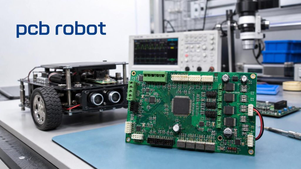
A PCB robot can mean a small robot built on a printed circuit board, a robot control board, or a PCB used inside a robotic system. For engineers and buyers, the real question is not only what the term means. The real question is whether the robot PCB can be manufactured, assembled, tested, and delivered without creating avoidable problems during prototype validation.
EBest Circuit (Best Technology) supports robot PCB and PCBA projects with PCB fabrication, component sourcing, SMT assembly, through-hole assembly, DFM review, inspection, testing coordination, and small-batch production. If your robotics project includes Gerber files, BOM, CPL, stackup notes, impedance requirements, assembly drawings, or test instructions, you can send them to sales@bestpcbs.com for engineering review before production starts.
pcb robot
Robot PCB manufacturing starts with a clear understanding of control, power, sensors, connectors, assembly, and testing requirements.

What Does PCB Robot Mean for Real Robotics Projects?

In real robotics projects, a PCB robot usually refers to the printed circuit board used inside a robot or robotic module. The board may control motors, read sensors, manage power, connect communication interfaces, or support firmware programming and testing.

The meaning can change by project type:

  • A student project may use a line follower robot PCB.
  • A mobile robot may use a motor control PCB.
  • An industrial robot may use controller, I/O, sensor, and power boards.
  • A robotic camera or inspection system may need high-speed signal routing.
  • A service robot may combine sensors, wireless modules, battery circuits, and compact connectors.

The risk is that a robot PCB is often judged only by whether the circuit works on paper. In production, the board also has to survive soldering, cable connection, vibration, current load, heat, enclosure limits, and repeated operation.

For this reason, a useful manufacturing review should connect the circuit files with the real working condition. A robot control board is not only a PCB layout. It is part of a moving product.

PCB Robot vs Robot PCB: Which Meaning Fits Your Project?

PCB robot and robot PCB are often used together, but they do not always describe the same thing.

PCB robot may describe:

  • A small robot built directly on a PCB
  • A foldable or structural PCB robot
  • A DIY robot board
  • A robotics-related printed circuit board
  • A robot used in PCB production

Robot PCB is usually clearer for manufacturing. It means a PCB used inside a robot system.

For EBest Circuit, the practical focus is robot PCB and robotics PCB manufacturing. The customer’s design team defines the circuit, firmware, MCU, sensor strategy, control logic, and robot function. Our role is to review whether the provided PCB and assembly files can move through fabrication, sourcing, SMT, inspection, testing, and packing reliably.


That distinction matters. If a customer asks us to create the full robot electronics design from scratch, that may go beyond our service scope. If the customer provides production files and needs manufacturing, assembly, DFM, BOM, and testing support, that is where EBest Circuit can help.

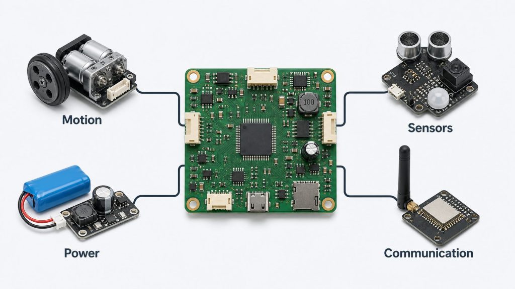
How a Robot PCB Connects Motion, Sensors, Power, and Communication

A robot PCB becomes valuable because it connects several demanding functions on one board.

pcb robot
A robot PCB often connects motion control, sensor input, power management, and communication interfaces on one board.

Motion control

Motor drivers, MOSFETs, relays, encoders, and connectors may carry current and receive fast control signals. If copper width, heat dissipation, solder joints, or connector strength are not reviewed, the robot may fail during movement rather than during simple bench testing.

Sensor input

Robotics boards often connect optical sensors, IR sensors, cameras, IMUs, encoders, ultrasonic sensors, pressure sensors, or current sensors. Sensor areas may be sensitive to connector direction, solder cleanliness, signal noise, and mechanical position.

Power management

Robots may use batteries, adapters, DC motors, regulators, charging circuits, and protection devices. A small power issue can cause reset, unstable motor behavior, overheating, or failed validation.

Communication

USB, CAN, UART, RS485, Ethernet, Wi-Fi, Bluetooth, or other interfaces may appear on the same board. If controlled impedance or differential routing is required, the stackup and impedance plan should be confirmed before fabrication.

This is why robot PCB manufacturing cannot be treated like a simple bare board order. The board must match the customer’s electrical files and the physical working environment.

PCB Design for Robotics: What Must Be Ready Before Manufacturing?

For PCB design for robotics, EBest Circuit does not replace the customer’s design team. However, before production starts, certain files must be clear enough for manufacturing.

The most useful customer file package includes:

  • Gerber or ODB++ files
  • Drill files
  • BOM
  • CPL or pick-and-place file
  • Assembly drawing
  • PCB drawing
  • Stackup requirement
  • Board thickness and tolerance
  • Copper thickness
  • Surface finish requirement
  • Impedance notes, if any
  • Firmware file, if programming is required
  • Test instructions
  • Packing notes

The problem is not only missing files. The bigger risk is inconsistency between files.

For example, a connector may face one direction in the assembly drawing but another direction in the CPL file. A BOM may list a component package that does not match the PCB footprint. A programming header may be present but blocked after assembly. A sensor may need edge alignment, but the panel design may make depaneling risky.

These are the kinds of issues that should be found before SMT starts, not after the customer receives the first prototype.

Robot Controller PCB Risks That Can Delay Prototype Validation

A robot controller PCB often becomes the first board the customer tests during bring-up, especially in a prototype circuit board assembly project. If it fails, the whole robot project slows down.

Common validation risks include:

  • Motor driver overheating
  • MCU or processor orientation errors
  • Unclear programming access
  • Sensor connector mismatch
  • Wrong polarity on power input
  • Weak solder joints on high-stress connectors
  • Insufficient copper for current paths
  • Missing or inaccessible test pads
  • BGA or QFN soldering defects
  • Board warpage or poor mechanical fit
  • Packing damage after assembly

A low-cost prototype can become expensive if debugging time is lost. Engineers may spend days checking firmware, motor drivers, sensors, or wiring before discovering the issue came from assembly, a wrong component, or an unclear production note.

EBest Circuit’s value is to catch practical manufacturing risks early. For robot controller PCB projects, our engineering review focuses on the details that affect whether the first assembled boards can enter customer testing smoothly.

How EBest Circuit Reduces Robot PCB Assembly Risks Before SMT

Robot PCB assembly is where many small file issues become real defects. Before SMT, EBest Circuit reviews the project as a complete build, not as separate documents.

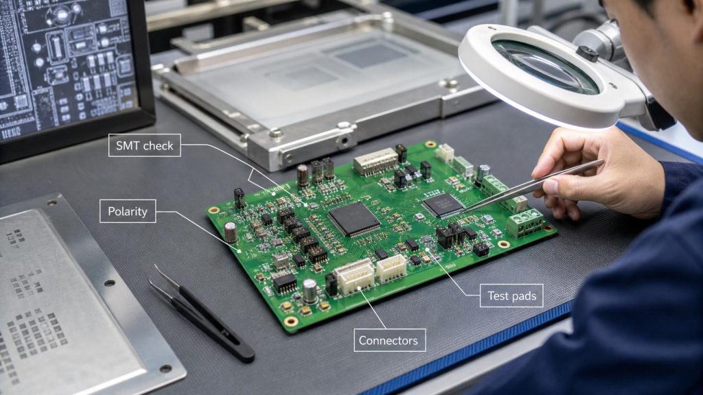
pcb robot
Before SMT, robot PCB assembly files should be checked for polarity, connector direction, test access, and process risks.

The review focuses on production risk:

  • Does the BOM match the PCB footprint?
  • Are connector directions clear?
  • Are polarity marks visible and consistent?
  • Are fine-pitch ICs suitable for the stencil and SMT process?
  • Does the panel support stable printing and placement?
  • Are BGA, QFN, or hidden solder joints expected?
  • Are through-hole parts and hand soldering notes clear?
  • Does the board need cleaning after assembly?
  • Is firmware programming required?
  • Does the customer define a functional test method?

This matters because robot PCBA projects often combine SMT parts, plug-in connectors, power parts, cables, programming interfaces, and test points. If one item is unclear, the board may still be assembled, but the customer may not be able to use it smoothly.

A good robot PCB assembly process is not only about placing components. It is about keeping the customer’s engineering intent visible until the board is packed and shipped.

Line Follower Robot PCB: Small Board, Real Manufacturing Risks

A line follower robot PCB is often used in education, competitions, and early robotics prototypes. It may look simple, but it still has real manufacturing risks.

Typical features include:

  • Microcontroller
  • Motor driver
  • IR sensor array
  • Battery input
  • Voltage regulator
  • Motor connectors
  • Programming header
  • LEDs or display
  • Mounting holes
  • Compact board outline

The main challenge is that the board is small, but the functional sensitivity is high.

If the sensor array is not positioned correctly, line detection may be unstable. If the motor current path is too narrow, heat or voltage drop may affect movement. If the battery connector or motor connector is weak, repeated plugging and movement may damage the solder joint. If test access is poor, debugging becomes slower.

For small robotics prototypes, EBest Circuit can review panelization, component direction, soldering process, connector strength, and inspection access before assembly. That helps the customer spend more time testing robot behavior and less time chasing avoidable production issues.

Robot PCB Manufacturing Details That Affect Reliability

Robot PCB manufacturing details can affect whether the board performs reliably after assembly.

Important reliability-related factors include:

  • Board thickness
  • Copper thickness
  • Material Tg
  • Via structure
  • Surface finish
  • Solder mask opening
  • Mounting hole plating
  • Connector pad strength
  • Thermal design around power parts
  • Controlled impedance for high-speed interfaces
  • Panel design for SMT
  • Electrical testing before assembly

For example, a robot board with motor drivers may need stronger attention to copper width, thermal relief, and high current PCB assembly requirements. A sensor board may need clean solder mask definition and stable connector placement. A compact controller with BGA or fine-pitch ICs may need better DFM review, AOI, and X-Ray planning.

EBest Circuit supports FR4 PCB, high-Tg PCB, HDI PCB, flex PCB, rigid-flex PCB, metal core PCB, ceramic PCB, heavy copper PCB, and impedance-controlled PCB projects. For robot PCB projects, the right process depends on the board’s current, density, mechanical space, and testing needs.

How Robotics PCBA Testing Helps Catch Problems Before Delivery

A robotics PCBA should be inspected and tested according to the project risk, with suitable PCB testing and assembly inspection methods. The purpose is not to make the process look complex. The purpose is to catch problems before the boards reach the customer’s test bench.

pcb robot
Robotics PCBA testing may include AOI, X-Ray, power-on checks, functional testing, and ESD-safe packing before delivery.

Possible inspection and test steps include:

  • Incoming material check
  • SPI after solder paste printing
  • AOI after reflow
  • X-Ray for BGA, QFN, or hidden solder joints
  • Visual inspection
  • Through-hole solder joint inspection
  • Bare PCB electrical test
  • Firmware programming, if customer provides firmware
  • Power-on check
  • Customer-defined functional test
  • Connector and polarity inspection
  • Final packing inspection

For robot PCBA projects, test points should be planned carefully. Power, ground, programming, communication, motor output, and key sensor signals may need accessible pads if the customer expects production testing.

A robot PCB should not only pass visual inspection. It should arrive ready for bring-up, movement testing, sensor connection, and next-stage validation.

PCB Robot Manufacturing Case Study for a USA Robotics Project

A USA customer needed a small batch of robot controller PCB assemblies for an indoor mobile robot prototype. The project was used for motion control validation before the customer moved toward pilot production.

Project requirements

  • Customer region: USA
  • Application: Indoor mobile robot controller
  • Quantity: 30 pcs prototype PCBA
  • PCB type: 4-layer FR4 robot controller PCB
  • Material: High-Tg FR4
  • Finished thickness: 1.6mm +/-10%
  • Copper thickness: 1oz finished outer copper
  • Surface finish: ENIG
  • Assembly: SMT + through-hole connectors
  • Main areas: MCU, motor driver, sensor connectors, power input, programming header
  • Test: Power-on check, connector inspection, customer-defined functional test points
  • Packing: Single-board ESD packaging after assembly

Main risks

  • The motor driver area needed stable soldering and heat awareness.
  • Sensor connectors had to face the correct direction for cable assembly.
  • Programming access had to remain usable after assembly.
  • Small-batch quantity still required clean SMT panelization.
  • The customer needed boards that could enter robot bring-up quickly.

EBest Circuit solution

  • Reviewed Gerber, BOM, CPL, assembly drawing, and connector notes together.
  • Confirmed polarity, Pin 1 direction, and connector orientation before SMT.
  • Reviewed panelization and fiducial marks for assembly accuracy.
  • Used AOI and visual inspection after SMT.
  • Checked through-hole connector solder joints after manual assembly.
  • Packed each assembled board separately to reduce handling damage.

Result

The customer received assembled robot controller boards prepared for power-on testing, firmware loading, sensor connection, and motor control debugging.

The value was not only producing 30 boards. The value was giving the customer a clearer manufacturing path from PCB fabrication to sourcing, SMT assembly, connector soldering, inspection, testing notes, and final packing.

Why Turnkey Support Matters for Robot PCB Projects

Robot PCB projects often involve more handoffs than customers expect. PCB fabrication, component sourcing, SMT assembly, through-hole soldering, programming, testing, and packing can each create risk if handled separately.

Turnkey support helps keep project details connected.

For example:

  • BOM risk can be checked before SMT scheduling.
  • PCB footprint and component package can be reviewed together.
  • Panelization can be planned for both fabrication and assembly.
  • Connector direction can stay visible from drawing review to inspection.
  • Test notes can be prepared before the boards are packed.
  • Packing requirements can match the assembled board’s connectors and components.

EBest Circuit has worked in PCB and PCBA manufacturing since 2006. The company serves customers in more than 40 countries and regions, with major export markets including the USA, Germany, and Israel. Quality support includes ISO9001, ISO13485, IATF16949, AS9100D, RoHS, REACH, and UL-related documentation.

For robotics customers, communication stability also matters. Many engineers, quality managers, production leaders, and sales members at EBest Circuit have worked in the company for more than 10 years. When a robot PCB prototype needs quick decisions, stable technical communication can reduce unnecessary delay.

FAQs About PCB Robot and Robot PCB Manufacturing

1. What does PCB robot mean?

PCB robot may mean a robot built on a printed circuit board, a robot-related PCB, or a PCB used inside a robot system. In manufacturing, it usually refers to robot PCB or robotics PCBA production.

2. What is a robot PCB?

A robot PCB is a printed circuit board used in a robot system. It may control motors, read sensors, manage power, connect communication interfaces, or support firmware programming and testing.

3. Can EBest Circuit design the full robot circuit?

EBest Circuit does not replace the customer’s full electronic design team. The customer should provide the circuit design, firmware, control logic, and product requirements. EBest Circuit supports PCB fabrication, DFM review, BOM sourcing, PCBA assembly, inspection, and testing coordination.

4. What files are needed for robot PCB assembly?

Useful files include Gerber or ODB++, BOM, CPL, assembly drawing, PCB drawing, stackup notes, impedance requirements, test instructions, firmware file if programming is needed, and packing notes.

5. Why is testing important for robotics PCBA?

Robotics boards may control motion, sensors, communication, and power. Testing helps catch open circuits, soldering defects, connector issues, polarity errors, programming access problems, and functional risks before delivery.

6. Can a line follower robot PCB be assembled in small batches?

Yes. A line follower robot PCB can be produced as a prototype or small batch. The files should still be reviewed for sensor position, motor current paths, connectors, board outline, component orientation, and test access.

All in all, a robot PCB project becomes easier to manage when fabrication, sourcing, assembly, inspection, and test notes stay connected. If you are preparing a PCB robot, robot controller PCB, sensor board, motor control PCB, or robotics PCBA project, send your files and project notes to sales@bestpcbs.com. EBest Circuit’s engineering team can review the manufacturing path before your boards move into production.

You may also like

AS9100 Certified PCB Fabrication for Aerospace PCBs

July 20th, 2026

AS9100 certified PCB fabrication is important when a PCB project needs more than standard board manufacturing. For aerospace electronics, avionics-related modules, high-reliability industrial systems, and other risk-sensitive products, customers often need controlled processes, clear documentation, material traceability, inspection records, and stable repeatability from prototype to production.

EBest Circuit (Best Technology) supports custom PCB fabrication, advanced aerospace PCBA, DFM review, component sourcing, testing, and documentation for customers who need reliable PCB and PCBA production. We hold ISO9001, ISO13485, IATF16949, and AS9100D certifications. If your project requires AS9100 certified PCB fabrication, stackup review, material control, impedance reporting, or assembly support, please feel free to send your Gerber files, drawings, stackup notes, BOM, inspection requirements, or production documents to sales@bestpcbs.com for engineering review before production.

as9100 certified pcb fabrication

What Is AS9100 Certified PCB Fabrication?

AS9100 certified PCB fabrication means the PCB manufacturer operates under a quality management system based on AS9100 requirements. AS9100 is widely used in aerospace and high-reliability manufacturing because it places strong attention on process control, risk management, traceability, documentation, supplier control, and continual improvement.

For PCB projects, AS9100 certified PCB fabrication is not only about the certificate on the supplier’s website. It should affect how the manufacturer handles the order from the first engineering review to final shipment.

In a practical PCB fabrication project, AS9100-related control may include:

AreaWhat Should Be Controlled
Engineering filesGerber, drawing, stackup, notes
MaterialsLaminate, copper, solder mask, finish
ProcessDrilling, plating, imaging, etching
InspectionElectrical test, visual inspection, reports
TraceabilityLot, material, production records
Change controlEQ, file confirmation, revision control

For customers, the value is simple: the PCB is made under a more disciplined system, and important production details are less likely to disappear between quotation, engineering review, fabrication, inspection, and delivery.

as9100 certified pcb fabrication

When Do Engineers Need AS9100 Certified PCB Fabrication?

Engineers usually need AS9100 certified PCB fabrication when the board will be used in products where quality records, repeatability, and traceability matter.

Typical situations include:

  • Aerospace electronics
  • Avionics-related modules
  • High-reliability control systems
  • Satellite or communication support equipment
  • Industrial monitoring devices
  • Automotive and transportation electronics
  • Medical or safety-related electronics
  • Long-life embedded systems

Not every PCB needs AS9100-level control. A simple consumer prototype may only need standard FR4 PCB fabrication. But when a board is used in a critical system, the customer may need more than a low-cost PCB supplier.

For example, an engineer may ask:

QuestionWhy It Matters
Can the material be traced?Needed for quality records
Can production files be confirmed first?Reduces file interpretation risk
Can test reports be provided?Supports customer documentation
Can changes be controlled?Prevents wrong revision builds
Can PCBA continue under one workflow?Reduces handoff risk

If these questions matter to your project, AS9100 certified PCB fabrication becomes more relevant than ordinary PCB ordering.

AS9100 PCB Fabrication vs ISO 9001 PCB Manufacturing

ISO 9001 is a general quality management system used across many industries. It is valuable for PCB manufacturing because it helps a supplier control processes, documentation, corrective actions, and customer requirements.

AS9100 builds on ISO 9001 and adds requirements that are more suitable for aerospace and high-reliability industries. That is why customers may specifically search for AS9100 PCB fabrication instead of only ISO 9001 PCB manufacturing.

ItemISO 9001 PCB ManufacturingAS9100 PCB Fabrication
Main useGeneral quality controlAerospace-level quality control
Risk focusStandard process riskStronger risk management
TraceabilityRequired where applicableMore strongly emphasized
DocumentationControlled recordsMore detailed production evidence
Supplier controlImportantMore rigorous
Customer confidenceGood baselineBetter fit for aerospace projects

This does not mean every AS9100 project is more complex in PCB structure. A 2-layer or 4-layer PCB may still need AS9100 control if the product application requires strict documentation and traceability.

The key difference is not only the board itself. It is the manufacturing discipline behind the board.

AS9100D PCB Quality Control and Traceability

AS9100D PCB quality control should cover the complete fabrication path. For a PCB manufacturer, this means the team should understand the customer’s technical files, confirm unclear requirements before production, and keep quality records visible throughout the build.

Important control points may include:

Control PointPractical Meaning
File reviewGerber, drawing, stackup, notes
EQ handlingConfirm unclear or conflicting details
Material reviewTg, copper, laminate, finish
Process controlDrilling, plating, solder mask, routing
Electrical testContinuity and isolation check
Final inspectionVisual and dimensional checks
ReportsCOC, electrical test, inspection records

Traceability is especially important. If a customer later asks about material batch, surface finish, copper thickness, test result, production version, or shipment record, the supplier should be able to find the information instead of relying on memory.

At EBest Circuit, digital production tracking helps connect material, batch, production progress, and quality records. For high-reliability PCB and PCBA projects, this makes communication clearer between engineering, production, inspection, and delivery.

What Aerospace Electronics Need from AS9100 Certified PCB Fabrication

Aerospace electronics usually need stable manufacturing control rather than only advanced PCB capability. Some aerospace PCB projects are high-layer HDI boards. Others may be standard multilayer FR4 boards. The common point is that customers expect disciplined handling of every requirement.

For AS9100 certified PCB fabrication, aerospace electronics may need:

  • Confirmed production files before manufacturing
  • Clear stackup and material review
  • Controlled copper thickness and board thickness
  • Stable surface finish such as ENIG
  • Impedance control when required
  • Electrical testing before shipment
  • Inspection records and COC reports
  • Controlled packing and delivery documentation
  • Consistent production from prototype to small batch

This is why the supplier’s engineering response matters. If a requirement is unclear, the manufacturer should raise an EQ before production. If the drawing, Gerber, stackup, and written notes do not fully match, the issue should be clarified early.

For aerospace-related projects, a small misunderstanding can become expensive later. Good AS9100 PCB fabrication support helps reduce this risk before the board enters production.

How to Verify AS9100 Certified PCB Fabrication Companies

When comparing AS9100 certified PCB fabrication companies, do not only check whether the supplier says “AS9100 certified.” A buyer should verify whether the supplier can support the real project requirements.

A practical supplier check can include:

CheckWhat to Ask
CertificationIs AS9100D valid and relevant?
PCB capabilityCan they build this stackup and finish?
DocumentationCan they provide required reports?
TraceabilityCan they track material and production lots?
Engineering reviewDo they check files before production?
PCBA supportCan they support assembly if needed?

It is also useful to ask how the supplier handles unclear engineering requirements. A reliable PCB manufacturer should not silently guess when there is a conflict between Gerber data, drawing notes, stackup files, or customer specifications.

For example, if the customer requires ENIG, controlled impedance, copper thickness reporting, and no production before file approval, the supplier should confirm these points before manufacturing starts.

The strongest AS9100 PCB supplier is not always the largest company. It is the one that can match the customer’s board complexity, documentation needs, delivery plan, and production risk.

How AS9100 PCBA Production Connects PCB Fabrication and Assembly

AS9100 PCBA production becomes important when the project does not stop at bare PCB fabrication. Many aerospace and high-reliability electronics projects need PCB manufacturing, component sourcing, SMT assembly, through-hole assembly, testing, inspection, cleaning, and packing under one coordinated workflow.

The handoff between PCB fabrication and assembly is often where mistakes happen. Important notes may be lost if bare PCB production, component sourcing, and assembly are handled by separate suppliers.

A one-stop PCB and PCBA workflow can help keep these items connected:

StageKey Control
PCB fabricationStackup, material, finish, testing
BOM sourcingApproved parts and alternatives
SMT assemblyPlacement, reflow, inspection
Through-holeManual or selective soldering
TestingFunctional or customer-defined tests
PackingESD protection and shipment notes

For AS9100 PCBA production, the goal is not only to assemble components. The goal is to keep the customer’s engineering notes visible from the bare board stage to final shipment.

EBest Circuit supports PCB fabrication, component sourcing, PCB assembly, DFM review, and testing coordination. This helps customers reduce communication gaps when a project moves from prototype validation to small-batch or production builds.

AS9100 PCB Assembly Documentation and Inspection Reports

AS9100 PCB assembly projects often need documentation that supports customer review, incoming inspection, or internal quality records. The exact reports depend on the customer’s drawing, purchase order, product application, and quality requirements.

Common documentation may include:

DocumentPurpose
COCConfirms order and production compliance
Electrical test reportConfirms bare board testing
Inspection reportSupports incoming quality review
Solderability reportConfirms soldering readiness
Copper thickness reportSupports fabrication control
Impedance reportRequired for controlled impedance
Material recordsSupports traceability
Packing recordConfirms shipment handling

Not every project needs every report. The best practice is to confirm documentation requirements before production starts.

For example, if the customer needs COC, electrical test report, solderability test report, and copper thickness report, these should be written clearly in the production notes. If impedance control is required, the impedance coupon and test report should be planned before fabrication.

Good documentation is not paperwork for its own sake. It helps the customer understand what was built, how it was controlled, and whether the delivered boards match the approved requirements.

AS9100 Certified PCB Fabrication Case Study

In one 2024 project record, EBest Circuit handled a U.S. customer’s multilayer FR4 PCB that was suitable as a good example for AS9100-style manufacturing control. The board itself was not only a normal FR4 order. The customer’s requirements showed the kind of discipline high-reliability customers often care about: file confirmation, IPC standard, test reports, electrical testing, and delivery quality.

Project Snapshot

ItemRequirement
Customer regionUnited States
PCB type4-layer FR4 PCB
MaterialTg170 FR4
Copper thickness2oz inner and outer copper
Board thickness1.6mm +/-10%
Surface finishENIG 1u”
Solder maskGreen solder mask, white silkscreen
Structure noteBlind via requirement
StandardIPC-6012 Class 2
ReportsCOC, electrical test, solderability, copper thickness
Testing100% continuity test before shipment

The important point in this project was not only the PCB specification. It was the control path.

Before production, the customer required production files to be provided and confirmed. This reduced the risk of building from misunderstood data. For a PCB with Tg170 material, 2oz copper, ENIG, blind vias, IPC-6012 Class 2 requirements, and shipment reports, early confirmation helped align engineering, production, and quality inspection.

EBest Circuit treated the project as a controlled manufacturing job rather than a simple quote-to-build order.

Key actions included:

  • Reviewing Gerber files, drawing notes, and production requirements
  • Confirming the stackup and fabrication notes before production
  • Checking the blind via requirement against the production process
  • Controlling Tg170 material, copper thickness, ENIG finish, and solder mask
  • Preparing required reports for shipment
  • Performing 100% continuity testing before delivery

For the customer, the value was not just receiving finished boards. The value was receiving boards with a clearer production trail: confirmed files, controlled fabrication, electrical test records, copper thickness reporting, solderability evidence, and shipment quality checks.

This is the type of practical support customers expect when AS9100 certified PCB fabrication is part of the sourcing decision.

as9100 certified pcb fabrication

Why Choose EBest Circuit for AS9100 Certified PCB Fabrication?

EBest Circuit (Best Technology) is not only a bare PCB supplier. We support customers with PCB fabrication, component sourcing, PCB assembly, DFM review, testing coordination, and documentation support.

For AS9100 certified PCB fabrication, our value is practical engineering support before and during production.

EBest Circuit support includes:

  • AS9100D, ISO9001, ISO13485, and IATF16949 certifications
  • Custom FR4 PCB, HDI PCB, rigid-flex PCB, metal core PCB, ceramic PCB, and high-frequency PCB manufacturing
  • Prototype, small-batch, and production support
  • DFM review before production
  • Stackup and material review
  • Controlled impedance support when required
  • Electrical testing and inspection support
  • Component sourcing and PCBA assembly
  • Documentation support based on customer requirements
  • Digital production traceability

For customers, this means fewer disconnected steps. A project can move from PCB file review to fabrication, sourcing, assembly, testing, packing, and delivery with one team coordinating the workflow.

This is especially useful when the customer needs engineering response, documentation clarity, stable quality, and fast communication.

FAQs about AS9100 Certified PCB Fabrication

1. What does AS9100 certified PCB fabrication mean?
AS9100 certified PCB fabrication means the PCB manufacturer operates under an AS9100 quality management system. For PCB projects, this supports stronger process control, documentation, traceability, risk management, and customer requirement control.

2. Is AS9100 certification required for every aerospace PCB?
Not always. The requirement depends on the customer, application, contract, and quality standard. However, many aerospace electronics customers prefer or require AS9100 certified PCB fabrication because it supports traceability and controlled production.

3. What is the difference between AS9100 PCB fabrication and ISO 9001 PCB manufacturing?
ISO 9001 provides a general quality management foundation. AS9100 adds aerospace-focused requirements such as stronger risk control, documentation, supplier control, and traceability. For high-reliability projects, AS9100 is often more relevant.

4. What documents may be needed for AS9100 PCB assembly?
Common documents may include COC, electrical test report, inspection report, solderability report, copper thickness report, material records, impedance report, and customer-defined inspection documents. The exact list should be confirmed before production.

5. Can EBest Circuit support both AS9100 PCB fabrication and PCBA production?
Yes. EBest Circuit supports PCB fabrication, component sourcing, SMT assembly, testing coordination, inspection, packing, and documentation support. Customers can send Gerber files, BOM, stackup notes, drawings, and quality requirements to sales@bestpcbs.com for review.

If your aerospace electronics, high-reliability PCB, or PCBA project requires AS9100 certified PCB fabrication, please feel free to contact sales@bestpcbs.com. EBest Circuit’s engineering team can help review your files, stackup, material requirements, reports, and assembly path before production starts, so your project can move from engineering files to finished boards with clearer control and fewer avoidable risks.

You may also like

Internet of Things Wireless Modules PCB Guide

July 16th, 2026

Internet of things wireless modules help connected products send and receive data through Wi-Fi, Bluetooth, LoRa, Zigbee, NB-IoT, LTE-M, cellular, or other wireless technologies. They are widely used in smart sensors, industrial monitoring devices, medical electronics, asset trackers, smart meters, gateways, wearable devices, and compact control systems.

For engineers, the wireless module itself is only one part of the product. The final performance also depends on the PCB, antenna area, power supply, connector reliability, SMT assembly, cleaning, testing, and production control. EBest Circuit (Best Technology) supports PCB manufacturing, DFM review, component sourcing based on approved BOM, PCBA assembly, inspection, and testing for IoT wireless module projects. If you are preparing an IoT PCB or IoT module PCB assembly project, send your Gerber files, ODB++ files, BOM, drawings, assembly notes, or testing requirements to sales@bestpcbs.com for engineering review before production.

internet of things wireless modules

What Are Internet of Things Wireless Modules?

Internet of things wireless modules are compact electronic modules that give a device wireless communication capability. Instead of building the full radio circuit from the beginning, many engineers use a ready-made wireless module that already includes key communication parts.

A typical IoT wireless module may include:

  • Wireless chipset
  • RF front-end circuit
  • Memory
  • Power management circuit
  • Crystal or oscillator
  • Shielding cover
  • Antenna connector or onboard antenna
  • Module pads for soldering to the main PCB
  • Firmware or communication stack support from the module supplier

The module allows the end product to connect to nearby devices, a gateway, a router, a cellular network, or a cloud platform. In a real product, the module usually sits on a carrier PCB or main control board with sensors, connectors, power circuits, MCU, interface circuits, and mechanical mounting features.

internet of things wireless modules

How Do IoT Wireless Modules Connect Devices?

IoT wireless modules connect devices by converting sensor, control, or system data into wireless signals. The module communicates with other devices, a local network, or a remote server depending on the selected wireless technology.

For example:

Wireless MethodCommon Use
Wi-FiHigh data rate, local internet access
BluetoothShort-range device connection
LoRaLong-range, low-power sensing
ZigbeeMesh networks and smart devices
NB-IoTLow-power cellular IoT
LTE-MMobile IoT with better data support
4G/5G cellularWide-area data connection

For PCB and PCBA manufacturing, the important point is that different wireless technologies create different board-level requirements. A Wi-Fi module may need careful antenna clearance. A cellular IoT module may need stronger power stability. A compact wearable product may need tight component placement and controlled mechanical size. A gateway may need connectors, shielding, thermal control, and reliable assembly.

internet of things wireless modules

Common Types of Wireless Modules for IoT Products

Wireless modules for IoT products are usually selected by the customer’s engineering team according to communication distance, data rate, power consumption, certification requirements, network availability, and product cost.

Common types include:

Wi-Fi modules
Used when the product needs local network access, higher data rate, and internet connectivity through routers or access points.

Bluetooth modules
Used for short-range communication, mobile app connection, wearable devices, handheld devices, and low-power accessories.

LoRa modules
Used for long-range, low-power sensing applications such as smart agriculture, metering, environmental monitoring, and remote sensors.

Zigbee modules
Used for mesh networks, smart home devices, building automation, lighting control, and low-power device networks.

NB-IoT and LTE-M modules
Used for low-power cellular IoT products that need wide-area coverage, such as smart meters, trackers, and industrial monitoring devices.

Cellular modules
Used for devices that need mobile network connectivity, higher coverage, or remote data transmission without relying on local Wi-Fi.

EBest Circuit does not need to choose the wireless protocol for the customer. Our role is to manufacture and assemble the PCB or PCBA according to the customer-approved design files, BOM, module selection, and production requirements.

internet of things wireless modules

Wi-Fi, Bluetooth, LoRa, and Cellular IoT Modules

Each IoT module type has different PCB manufacturing and assembly concerns.

Wi-Fi and Bluetooth modules often operate in the 2.4GHz band, so antenna position and keep-out areas matter. If the antenna area is blocked by copper, metal housing, battery, connector, or enclosure structure, wireless performance may be affected.

LoRa modules are often used in low-power, long-range products. These projects may care more about battery life, stable solder joints, connector reliability, and outdoor or industrial operating conditions.

Cellular IoT modules may require stronger power handling, good grounding, reliable SIM/eSIM related areas, antenna connector assembly, and careful inspection after SMT. Power peaks, vibration, and connector contact can matter more in field-deployed products.

For all these modules, the PCB manufacturer should not change RF layout, antenna geometry, or matching circuits without customer approval. However, the manufacturer should review manufacturability risks such as pad design, solder mask opening, panelization, stencil, SMT process, connector placement, and inspection points.

internet of things wireless modules

Internet of Things Wireless Modules PCB Requirements

Internet of things wireless modules place several practical requirements on PCB manufacturing.

The PCB must support the module footprint accurately. If the pad size, solder mask opening, stencil design, or assembly process is not suitable, the module may shift, tombstone nearby components, bridge, or form weak solder joints.

Important PCB requirements include:

PCB AreaWhat to Check
Module footprintPad size and solderability
Antenna zoneKeep-out and copper clearance
Power pathStable supply and copper width
GroundingClean return path and shielding support
ConnectorsMechanical strength and alignment
Surface finishENIG or suitable solderable finish
PanelizationSMT efficiency and board protection
Test pointsEasier inspection and testing

For high-density IoT products, the PCB may also require HDI, blind vias, fine line/space, impedance review, rigid-flex construction, or special thickness control. These points should be confirmed before production starts.

IoT Module PCB Layout and Manufacturing Checks

IoT module PCB layout should be reviewed from a manufacturing and assembly point of view before the board enters production. This does not mean changing the customer’s circuit design. It means checking whether the provided files can be manufactured and assembled reliably.

Key checks include:

  • Is the wireless module footprint correct?
  • Are module pads suitable for SMT assembly?
  • Is the antenna keep-out area clearly defined?
  • Are large copper areas balanced enough for soldering?
  • Are vias too close to module pads or connectors?
  • Are test points accessible?
  • Is the board shape suitable for panelization?
  • Are castellated holes, edge connectors, or antenna connectors manufacturable?
  • Does the drawing match the Gerber and BOM?
  • Are special notes clear before production?

For IoT wireless module products, many issues are not caused by the wireless module itself. They come from small manufacturing details: poor solder paste control, unclear assembly notes, tight connector spacing, weak panel support, insufficient test access, or missing inspection requirements.

PCBA Assembly for IoT Wireless Modules

PCBA assembly is a key part of IoT wireless module production. Wireless modules may be shielded, relatively large, heat-sensitive, or sensitive to solder paste volume. Some products also include fine passive components, sensors, connectors, LEDs, buttons, battery holders, SIM card holders, or antenna connectors on the same board.

During IoT wireless module PCBA assembly, EBest Circuit can support:

  • Component sourcing based on approved BOM
  • SMT assembly
  • Connector assembly
  • Solder paste and stencil review
  • Module placement inspection
  • AOI inspection
  • X-ray inspection when required
  • Functional testing coordination
  • Cleaning and packing requirements
  • Prototype and small-batch production

The most important point is process visibility. The module, PCB, BOM, SMT, testing, and packing requirements should be handled as one project, not as separate disconnected steps.

Testing and Reliability for IoT Wireless Module Products

IoT wireless module products are often used in real environments, not only on a lab bench. They may be installed inside industrial equipment, medical devices, smart meters, outdoor sensors, gateways, access control devices, or portable products.

Reliability checks may include:

Reliability AreaTypical Concern
Solder jointsModule and connector strength
Power stabilityStable module operation
RF areaNo unwanted copper or obstruction
CleanlinessNo residue near fine components
ConnectorsContact and insertion reliability
EnvironmentHeat, humidity, vibration, enclosure fit
TraceabilityProduction and batch records

Some testing is defined by the customer, such as functional testing, communication testing, programming, current measurement, LED status check, or connector inspection. EBest Circuit can coordinate PCBA testing according to the customer’s approved test method and production requirements.

IoT Wireless Module PCB Manufacturing Case Study

A European industrial customer needed a 6-layer FR4 PCB for an IoT wireless monitoring product used in equipment data collection. The wireless module and circuit design were already defined by the customer. EBest Circuit’s role was to review the manufacturing files, confirm the production stackup, control the impedance-related requirements, and fabricate the PCB according to the approved documents.

Project requirements

  • 6-layer FR4 PCB
  • IT180 material, with Isola 370HR or equivalent material required
  • Outer copper: 1oz
  • Inner copper: 0.5oz
  • Board thickness: 1.6mm ±10%
  • Surface finish: ENIG, Au 1u”
  • Green solder mask, white silkscreen
  • Differential impedance requirement according to the customer’s PDF specification
  • Bare PCB delivery
  • Factory panelization allowed
  • Production files had to be sent to the customer for confirmation before manufacturing

Why this project needed careful review

This was not a simple FR4 board order. For an IoT wireless module product, the PCB had to support stable signal transmission, reliable assembly, and predictable production quality.

The first checkpoint was the material. The customer specified IT180 and allowed Isola 370HR or equivalent material, so the material choice had to be confirmed before production.

The second checkpoint was impedance. Because the customer required differential impedance, EBest Circuit had to review the stackup, copper thickness, dielectric structure, and impedance notes in the customer’s PDF specification before fabrication.

The third checkpoint was documentation. The customer required production files to be confirmed before manufacturing. This helped make sure the stackup, material, copper thickness, surface finish, panelization, and impedance requirements were aligned before the board entered production.

EBest Circuit’s manufacturing support

  • Reviewed Gerber files, drawing, and customer PDF specification
  • Prepared production stackup and production files for customer confirmation
  • Checked material requirement: IT180 / Isola 370HR equivalent
  • Reviewed differential impedance requirements before fabrication
  • Confirmed copper thickness, board thickness, ENIG, solder mask, and silkscreen
  • Arranged factory panelization for bare PCB production
  • Controlled the project according to the approved production documents

For the customer, the value was not only receiving a 6-layer PCB. The important value was that the manufacturing details were reviewed before production started. Material, impedance, stackup, copper thickness, finish, and panelization were confirmed first, helping reduce risk for the IoT wireless module product before assembly and system validation.

Why Choose EBest Circuit for IoT Wireless Module PCB and PCBA?

EBest Circuit is suitable for customers who need PCB and PCBA manufacturing support for IoT wireless module products, especially when the project needs more than bare PCB fabrication.

Customers choose EBest Circuit because we can support:

  • PCB fabrication
  • Component sourcing based on approved BOM
  • SMT assembly
  • Connector assembly
  • DFM review before production
  • BOM optimization suggestions
  • Prototype and small-batch support
  • PCBA inspection and testing coordination
  • One-stop PCB + sourcing + IoT PCB assembly turnkey service
  • ISO9001, ISO13485, IATF16949, and AS9100D quality systems
  • Digital workshop traceability

For IoT wireless modules, this one-stop support is useful because many production risks happen between steps. A footprint issue, BOM substitution, connector mismatch, antenna clearance mistake, or unclear test note can affect the final product. EBest Circuit helps keep these details visible from engineering review to shipment.

If you are building an IoT wireless module product, send your Gerber files, ODB++ files, BOM, drawings, module datasheet, assembly notes, testing method, or packing requirements to sales@bestpcbs.com. Our engineering team can help review the PCB and PCBA manufacturing path before production starts.

FAQs about Internet of Things Wireless Modules

1. What are internet of things wireless modules?

Internet of things wireless modules are compact communication modules that help devices connect through Wi-Fi, Bluetooth, LoRa, Zigbee, NB-IoT, LTE-M, cellular, or other wireless technologies.

2. What is the difference between IoT modules and wireless modules?

A wireless module provides communication capability. An IoT module is usually a wireless module used inside a connected product, often with sensors, power circuits, MCU, firmware, and cloud or gateway communication.

3. Can EBest Circuit design the wireless module circuit?

EBest Circuit mainly supports PCB manufacturing, DFM review, component sourcing based on approved BOM, PCBA assembly, inspection, and testing coordination. We manufacture and assemble according to customer-approved design files, BOM, and production requirements.

4. What should I prepare for an IoT wireless module PCBA project?

You should prepare Gerber or ODB++ files, BOM, placement file, drawings, module datasheet, assembly notes, testing instructions, firmware or programming notes if needed, and packing requirements.

5. Why is PCB manufacturing important for IoT wireless modules?

The PCB affects module soldering, antenna area, power stability, connector reliability, test access, mechanical fit, and production yield. A good manufacturing review helps reduce risk before SMT assembly.

Need help with an IoT wireless module PCB or PCBA project? Pls feel free to send your Gerber files, ODB++ files, BOM, module datasheet, drawings, assembly notes, or test requirements to sales@bestpcbs.com. EBest Circuit’s engineering team can help review the PCB and PCBA manufacturing path before production starts.

You may also like

Top 10 Rigid Flex PCB Manufacturers in China for Medical Electronics

July 16th, 2026

Choosing a rigid flex PCB manufacturer is not only about finding a supplier that can fabricate flexible and rigid materials together. For medical electronics, industrial sensors, compact modules, aerospace electronics, and high-density devices, the manufacturer must understand stackup control, bend reliability, impedance, material selection, surface finish, assembly, documentation, and traceability.

EBest Circuit (Best Technology) supports rigid-flex PCB manufacturing, DFM review, component sourcing, PCBA assembly, inspection, and production documentation for custom projects. If you require rigid-flexible PCB made in China, you can send your Gerber files, ODB++ files, stackup drawing, impedance notes, BOM, assembly notes, or special quality requirements to sales@bestpcbs.com. Our engineering team can help review the manufacturing path before production starts.

Rigid flex pcb manufacturer

What Makes a Good Rigid Flex PCB Manufacturer?

A good rigid flex PCB manufacturer should be able to handle both the electrical and mechanical risks of the board. Rigid-flex PCB is different from a standard FR4 PCB because the flex area is not only a routing area. It is also a bending, folding, or space-saving structure inside the final product.

When evaluating a supplier, focus on the points that affect real production:

CheckpointWhy It Matters
StackupControls thickness, impedance, and lamination risk
Flex materialAffects bend reliability and lifetime
Bend areaPrevents copper cracking and stress concentration
ImpedanceSupports high-speed signal stability
Surface finishAffects solderability and connector reliability
PCBA supportReduces handoff risk after fabrication
DocumentationImportant for medical and industrial projects

For medical electronics, the best supplier is usually not the cheapest one. It is the one that can identify risk before production starts.

Top 10 Rigid-Flex PCB Manufacturers in China

This list is not a formal revenue ranking. It is a practical buyer-oriented list of rigid-flex PCB manufacturers and PCB suppliers commonly considered by engineers sourcing from China or China-based supply chains.

1. EBest Circuit (Best Technology)

  • EBest Circuit is suitable for customers who need rigid-flex PCB manufacturing plus one-stop PCB and PCBA support. The company supports custom PCB fabrication, component sourcing based on approved BOM, SMT assembly, DFM review, testing, and documentation. For medical electronics, automotive electronics, aerospace electronics, industrial modules, and compact devices, EBest Circuit’s value is in engineering review and production coordination, not only bare board fabrication.
  • Best fit: rigid-flex PCB, FPC, HDI, FR4 PCB, ceramic PCB, metal core PCB, PCBA assembly, prototype, small batch, and production projects.

2. PCBWay

  • PCBWay is widely known for online PCB prototyping and custom PCB manufacturing. It is often considered by engineers who need fast quoting, broad PCB service coverage, and flexible prototype support. For rigid-flex PCB projects, it can be useful for prototype-stage sourcing, but complex medical or high-reliability projects still need careful review of drawings, stackup, test requirements, and assembly expectations.
  • Best fit: online PCB quoting, prototypes, small-batch rigid-flex PCB, and general PCB manufacturing.

3. JLCPCB

  • JLCPCB is popular among engineers, makers, and product teams because of its online ordering system, fast prototype service, and integration with component sourcing and assembly workflows. It is often a strong option for standard PCB prototypes and cost-sensitive development. For more complex rigid-flex PCB or high-reliability medical electronics, buyers should confirm material, tolerance, stackup, inspection, and documentation requirements before placing an order.
  • Best fit: fast prototypes, standard PCB fabrication, cost-sensitive projects, and early-stage validation.

4. Hemeixin Electronics

  • Hemeixin is known in the PCB market for advanced PCB manufacturing, including HDI, rigid-flex, and high-layer-count boards. It is often considered when the project requires more advanced fabrication capability than a simple prototype board. For engineers working on compact electronics, its strength is usually in more complex board structures.
  • Best fit: HDI PCB, rigid-flex PCB, high-density routing, and advanced multilayer PCB projects.

5. RayPCB

  • RayPCB provides a wide PCB manufacturing range, including rigid PCB, flexible PCB, rigid-flex PCB, HDI PCB, RF PCB, and PCBA services. It is often visible in search results for technical PCB topics and manufacturing guides. Buyers can consider it when comparing suppliers for rigid-flex capability, but should still validate project-specific requirements such as impedance, material, layer count, IPC class, and assembly details.
  • Best fit: broad PCB manufacturing, rigid-flex PCB, HDI PCB, RF PCB, and PCB assembly.

6. Viasion Technology

  • Viasion positions itself as a PCB and PCBA supplier with rigid-flex PCB manufacturing support. It can be considered by customers comparing China-based rigid-flex suppliers with assembly capability. For complex applications, buyers should check whether the supplier can support the exact stackup, flex construction, impedance, surface finish, and inspection documents required.
  • Best fit: rigid-flex PCB, PCB assembly, custom PCB projects, and turnkey support.

7. PCBONLINE

  • PCBONLINE is often considered for multilayer PCB, HDI PCB, rigid-flex PCB, and special PCB projects. It may be suitable for customers looking for technical manufacturing support rather than only standard low-cost PCB prototypes. For higher-reliability products, engineering confirmation before production is important.
  • Best fit: multilayer PCB, HDI PCB, rigid-flex PCB, and special PCB manufacturing.

8. NextPCB

  • NextPCB is another online-accessible PCB supplier that supports PCB fabrication and assembly services. It is often considered for prototype and small-batch PCB projects. For rigid-flex PCB projects, customers should provide clear drawings, bend requirements, stackup notes, and material requirements before production.
  • Best fit: prototype PCB, small-batch PCB, PCB assembly, and online sourcing.

9. MOKO Technology

  • MOKO Technology provides electronics manufacturing and PCB assembly services. It may be considered when the project needs more than bare PCB fabrication, especially if the customer needs PCBA, testing, and product-level manufacturing support. For rigid-flex projects, the manufacturing details should be confirmed based on the exact board structure.
  • Best fit: PCB assembly, electronics manufacturing, turnkey support, and small-to-medium production.

10. ALLPCB

  • ALLPCB is known as an online PCB manufacturing platform with prototype and batch PCB services. It may be useful for standard projects and early-stage comparisons. For medical electronics or complex rigid-flex PCB, customers should confirm whether the project requirements fit the supplier’s process capability before ordering.
  • Best fit: online PCB manufacturing, prototype PCB, batch PCB, and general PCB sourcing.

Best Rigid Flex PCB Manufacturer for Medical Electronics

For medical electronics, a rigid-flex PCB manufacturer should understand that the board is part of a reliability chain. The PCB may sit inside a handheld diagnostic device, wearable medical sensor, imaging module, monitoring device, or compact electronic instrument. In these products, a small manufacturing issue can affect assembly yield, connector stability, signal quality, or long-term reliability.

A medical electronics rigid-flex PCB project often needs stable material selection, controlled board thickness, reliable flex-to-rigid transition areas, clean ENIG surface finish, controlled impedance when signals require it, SMT assembly support, inspection records, and traceable production documentation.

EBest Circuit is a strong fit when the customer needs both PCB manufacturing and PCBA coordination. With ISO9001, ISO13485, IATF16949, and AS9100D certifications, EBest Circuit can support customers who need stronger quality management and documentation awareness for medical, automotive, aerospace, and industrial electronics.

Semi-Flex PCB vs Rigid-Flex PCB

Semi-flex PCB and rigid-flex PCB are sometimes confused, but they are not the same.

ItemSemi-Flex PCBRigid-Flex PCB
MaterialThin FR4 bending areaFR4 + PI flex layers
FlexibilityLimited bendingMore reliable bending
CostLowerHigher
Bend useUsually installation onlyFolding or controlled flex use
Best forSimple 3D fitCompact reliable modules

Semi-flex PCB can be useful when the board only needs to bend slightly during installation. Rigid-flex PCB is better when the product needs a more reliable flex section, a smaller assembly volume, fewer connectors, or more stable long-term performance.

If a project involves repeated bending, tight space, fine-pitch assembly, impedance control, or medical electronics, rigid-flex PCB is usually the safer choice.

Rigid Flex PCB Manufacturing Process Explained

Rigid flex PCB manufacturing is more complex than standard rigid PCB manufacturing because the board contains both rigid and flexible areas. The process must control lamination, drilling, plating, coverlay, solder mask, surface finish, outline, and testing without damaging the flex area.

A typical rigid-flex PCB manufacturing process includes:

StepKey Control
File reviewGerber, drawing, stackup, bend notes
Material prepFR4, PI, coverlay, stiffener, low-flow PP
Inner layersCopper balance and fine lines
LaminationThickness and resin flow
DrillingMechanical holes, laser vias, blind/buried vias
PlatingHole reliability and copper thickness
CoverlayFlex protection and opening accuracy
Solder maskRigid area solder mask control
Surface finishENIG or project-specified finish
TestingE-test, impedance test, inspection

The most important step is early engineering review. If the stackup, bend area, or impedance structure is not reviewed before production, problems may only appear after lamination or assembly, when correction is much more expensive.

Rigid-Flex PCB Stackup and Material Selection

Rigid-flex PCB stackup defines how rigid layers and flexible layers connect. It affects board thickness, bend radius, impedance, mechanical reliability, assembly process, and final product fit.

A rigid-flex PCB stackup may include FR4 rigid core, polyimide flexible core, adhesive or adhesiveless flex material, copper foil, coverlay, low-flow prepreg, stiffener, and ENIG or another surface finish.

For rigid-flex PCB, the bend area should avoid unnecessary copper stress. Traces in the flex area should be routed smoothly, with suitable spacing and without sharp corners. If the product has controlled impedance, the manufacturer must calculate the trace geometry based on the actual stackup, dielectric thickness, copper thickness, and reference layer.

Medical electronics, sensors, imaging products, and compact modules often need a balance between thin structure, stable impedance, reliable bending, and manufacturable assembly.

EBest Circuit Rigid-Flex PCB Manufacturing Capabilities

EBest Circuit supports rigid-flex PCB manufacturing for prototype, small-batch, and production projects where the board needs both mechanical flexibility and stable electrical performance. For many customers, the key question is not only whether a supplier can make a rigid-flex PCB, but whether the supplier can review the stackup, flex area, impedance, material, surface finish, panel delivery, and PCBA requirements before production starts.

Here are some rigid-flex PCB manufacturing capabilities that EBest Circuit can support or review according to project requirements:

CapabilityEBest Circuit Support
Rigid-flex layers2 to 20 layers
Finished thickness0.3mm to 3.0mm
Thickness tolerance>1.0mm: ±10%; ≤1.0mm: ±0.10mm
Flex structureInner or outer flex layer support
Flex materialsPI, adhesiveless flex core, coverlay, stiffener
Rigid materialsFR4, high Tg FR4, low-flow PP
Fine featuresFine line/space, BGA pads, laser vias, mechanical drilling
ImpedanceControlled impedance review; typical tolerance ±10%
Surface finishENIG and other finishes based on project needs
PCBA supportBOM sourcing, SMT assembly, connector assembly, testing, packing

For rigid-flex PCB projects, EBest Circuit pays special attention to the areas that often create risk: rigid-flex transition zones, bend areas, copper balance, coverlay openings, stiffener placement, impedance traces, drilling structure, and panelization for assembly.

This support is useful for customers developing medical electronics, industrial sensors, compact modules, aerospace electronics, automotive electronics, wearable devices, and other products where the PCB must fit into limited mechanical space while still supporting reliable assembly and signal performance.

Rigid-Flex PCB Manufacturing Case Study

A customer from Europe needed a high-layer rigid-flex PCB for a compact medical electronics module. The product required a thin structure, stable impedance, reliable bending performance, and controlled documentation before production.

Project requirements

  • 14-layer rigid-flex PCB
  • Tg180 material
  • ENIG 1u”
  • Green solder mask, white silkscreen
  • Total thickness: 1.4mm ±10%
  • Controlled impedance: 85 ohm ±10%
  • Date code beside the logo in DD-MM-YYYY format
  • Panel delivery required
  • Production stackup and production files had to be confirmed by the customer before manufacturing

Main manufacturing challenges

The first challenge was the stackup. A 14-layer rigid-flex PCB cannot be treated like a standard multilayer rigid board. The rigid area, flex area, dielectric thickness, copper thickness, and bonding materials all had to be reviewed together.

The second challenge was impedance control. Because the customer required 85 ohm ±10%, the stackup and trace geometry had to be checked before production, not only measured after the board was finished.

The third challenge was documentation control. For this project, EBest Circuit needed to prepare the production stackup and production files first, send them to the customer for confirmation, and then arrange manufacturing after approval.

EBest Circuit’s manufacturing support

  • Reviewed the customer’s original stackup reference before production
  • Prepared a production stackup for customer confirmation
  • Checked impedance feasibility based on the final production structure
  • Confirmed ENIG, solder mask, silkscreen, date code, and panel delivery requirements
  • Controlled the rigid-flex transition area to reduce manufacturing risk
  • Managed the project under a documented PCB production process

For the customer, the value was not only receiving a 14-layer rigid-flex PCB. The more important value was that the key production details were confirmed before fabrication started: stackup, impedance, material, date code, panel format, and manufacturing files. This helped reduce communication gaps and made the project easier to move from engineering review to production.

Why Choose EBest Circuit as Your Reliable Rigid Flex PCB Manufacturer?

EBest Circuit is suitable for customers who need a rigid flex PCB manufacturer that can support both manufacturing and assembly-related project control.

Customers choose EBest Circuit for rigid-flex PCB projects because the team can support PCB fabrication and PCBA assembly in one workflow, engineering review before production, DFM checking for manufacturability risks, BOM sourcing based on the approved BOM, SMT assembly, connector assembly, prototype and small-batch production, documented quality control, and digital production traceability.

For medical electronics and compact modules, this one-stop support can reduce handoff problems between PCB fabrication, assembly, inspection, and final delivery.

If you are developing a rigid-flex PCB project, you can send your Gerber files, ODB++ files, drawings, stackup, impedance notes, BOM, assembly notes, or quality requirements to sales@bestpcbs.com. EBest Circuit’s engineering team can help review the manufacturing path before production starts.

FAQs about Rigid Flex PCB Manufacturer

1. What is a rigid flex PCB manufacturer?

A rigid flex PCB manufacturer produces circuit boards that combine rigid PCB sections and flexible PCB sections in one structure. These boards are used when the product needs compact assembly, bending, folding, or fewer connectors.

2. How do I choose a rigid flex PCB manufacturer?

Choose a supplier that can review stackup, flex material, bend area, impedance, surface finish, PCBA requirements, and documentation before production. For medical electronics, quality systems and traceability are also important.

3. What is the difference between semi-flex PCB and rigid-flex PCB?

Semi-flex PCB usually uses a thinner FR4 bending area and is suitable for limited bending. Rigid-flex PCB uses flexible PI material and is better for products that need stronger bending reliability or compact 3D assembly.

4. Can rigid-flex PCB support controlled impedance?

Yes. Rigid-flex PCB can support controlled impedance, but the stackup, trace width, dielectric thickness, copper thickness, and reference layer must be reviewed before production.

5. Is rigid-flex PCB suitable for medical electronics?

Yes. Rigid-flex PCB is widely used in compact medical electronics, wearable devices, monitoring modules, and diagnostic equipment. The key is choosing a manufacturer that can support material control, stackup review, assembly, testing, and documentation.

Need help with a rigid-flex PCB project? If your project involves rigid-flex stackup, bend area reliability, controlled impedance, ENIG finish, PCBA assembly, or production documentation, send your Gerber files, ODB++ files, drawings, stackup notes, BOM, or assembly requirements to sales@bestpcbs.com. EBest Circuit’s engineering team will help review the manufacturing path before production starts.

You may also like

Ceramic PCB for RF: Substrate Materials, Design Benefits, and Manufacturing Guide

July 10th, 2026

What Is a Ceramic PCB for RF?

A ceramic PCB for RF is a circuit board or substrate used in high-frequency circuits where dielectric stability, low signal loss, dimensional accuracy, and thermal reliability matter more than standard PCB cost.

Ceramic PCB for RF modules, microwave filters, sensors, and power amplifiers

In RF and microwave applications, the substrate is part of the electrical design. It affects impedance, insertion loss, resonance behavior, signal phase, and long-term stability. This is why engineers often consider ceramic PCB substrate options such as alumina PCB for RF modules, microwave circuits, filters, sensors, power amplifiers, and hybrid circuits.

Why Ceramic PCB Substrate Matters in RF Circuits?

A ceramic PCB substrate matters in RF circuits because high-frequency signals are sensitive to material behavior. Small changes in dielectric constant, trace geometry, surface quality, or substrate thickness can shift impedance and affect performance.

For buyers, the key point is simple: RF ceramic PCB is not selected only for heat dissipation. The material must support stable signal behavior at the target frequency. A supplier must understand both ceramic PCB manufacturing and the RF requirements behind the drawing.

Key RF Properties: Dielectric Constant, Loss Tangent, and Dimensional Stability

For RF ceramic PCB projects, three material properties usually matter most: dielectric constant, loss tangent, and dimensional stability.

Ceramic PCB for RF modules, microwave filters, sensors, and power amplifiers
RF PropertyWhy It MattersBuyer Note
Dielectric constantAffects impedance, wavelength, trace width, and circuit sizeConfirm the value required by the RF design, not only the material name
Loss tangentAffects signal loss at high frequencyLower loss is more important as frequency increases
Substrate thicknessAffects impedance and manufacturable line widthKeep thickness controlled and clearly specified
Dimensional stabilityHelps maintain trace geometry and circuit repeatabilityImportant for filters, antennas, resonators, and microwave circuits
Surface qualityAffects metallization and high-frequency current behaviorReview finish and metallization process early

A good RF ceramic PCB quote should not start with “Can you make ceramic PCB?” It should start with frequency range, impedance target, material requirement, line width, tolerance, and metallization needs.

Common Materials: Alumina PCB, AlN, Rogers, and FR4

Material choice depends on frequency, loss target, thermal demand, cost, and manufacturing method. Alumina PCB is common in RF ceramic substrate applications, but it is not the only option.

MaterialRF StrengthLimitationBest Use
Alumina PCBStable ceramic substrate, good mechanical and thermal behavior, widely used in RF and hybrid circuitsHigher dielectric constant than many organic RF laminates; design must account for itRF modules, microwave circuits, sensors, hybrid circuits
Aluminum nitride PCBBetter thermal conductivity than aluminaHigher cost; not always needed for RF unless heat is also a major issueRF power modules, high-power microwave circuits, compact thermal designs
Rogers / PTFE-based RF laminateCommon for RF PCB design, lower-loss options availableMaterial and processing cost can be higher than FR4; thermal/mechanical behavior differs from ceramicAntennas, RF boards, microwave circuits, communication devices
FR4Low cost and easy to manufactureLoss and dielectric variation become problematic at higher frequenciesLow-frequency or cost-sensitive circuits where RF loss is acceptable

For many RF ceramic PCB projects, alumina PCB is selected when the design needs ceramic stability, precision metallization, and reliable high-frequency behavior in a compact substrate.

Ceramic PCB for RF vs Standard RF PCB Materials

The decision between ceramic PCB and standard RF laminate depends on circuit function, frequency, power level, size, and reliability environment.

OptionAdvantageLimitationBetter Fit
Ceramic PCB for RFStable substrate, good thermal behavior, suitable for hybrid and precision circuitsHigher cost and stricter manufacturing limitsRF modules, microwave packages, high-stability circuits
Rogers RF PCBMature RF laminate option with known dielectric choicesNot ceramic; thermal and mechanical behavior differAntennas, RF communication boards, microwave PCB layouts
FR4 RF designLow cost and fast productionHigher loss and less predictable dielectric behavior at high frequencyLow-frequency RF, simple prototypes, cost-sensitive products
RF performance comparison between ceramic PCB, Rogers laminate, and FR4 board

The practical takeaway: use FR4 only when RF loss and dielectric variation are acceptable. Use Rogers-type RF laminates for many standard RF boards. Use ceramic PCB when the design needs ceramic stability, compact structure, precision, or stronger thermal reliability.

Ceramic PCB Manufacturing Considerations for RF Applications

Ceramic PCB manufacturing for RF applications must control the details that affect signal performance. A small trace width error may be more serious in RF than in a normal power or control PCB.

Important manufacturing points include:

  • Substrate material and thickness control
  • Fine line and spacing capability
  • Metallization method, such as thick film, thin film, DBC, or other suitable process
  • Copper or conductor thickness
  • Surface roughness and finish
  • Dimensional tolerance
  • Via and hole quality if required
  • Flatness and warpage
  • Pattern registration
  • Cleanliness and handling

For RF ceramic PCB manufacturing, the supplier should review whether the requested geometry is manufacturable before production. If the layout uses very fine traces, tight impedance targets, or microwave structures, early engineering communication reduces prototype failure risk.

When Should You Choose Alumina PCB for RF?

Choose alumina PCB for RF when the circuit needs a stable ceramic substrate, good dimensional control, and reliable behavior in a compact or harsh environment.

Alumina PCB is often suitable for:

  • RF hybrid circuits
  • Microwave modules
  • Sensor circuits
  • Thin film or thick film RF substrates
  • Filters and matching networks
  • High-temperature or high-reliability electronics
  • Compact modules where ceramic stability is useful

Alumina may be unnecessary if the circuit can meet RF performance with a standard RF laminate at lower cost. It may also be the wrong choice if the design requires a different dielectric constant, lower loss material, or stronger thermal conductivity than alumina can provide.

Common Design and Purchasing Mistakes

The most common mistake is treating RF ceramic PCB like a normal ceramic circuit board. RF performance depends on both material and geometry.

Common RF ceramic PCB mistakes including incorrect dielectric constant, loose tolerance, and missing frequency details
MistakeWhy It Causes ProblemsBetter Approach
Only asking for “ceramic PCB for RF”Supplier cannot confirm material, frequency, or processProvide frequency range, substrate material, and circuit function
Ignoring dielectric constantImpedance and trace width may shiftSpecify target dielectric constant or approved material
Ignoring loss tangentHigh-frequency loss may become unacceptableDefine frequency and acceptable RF performance
Using vague tolerancesRF traces may not match design intentSpecify line width, spacing, substrate thickness, and dimensional tolerance
Choosing alumina automaticallyAlumina may not fit every RF designCompare alumina, AlN, Rogers, and FR4 based on real requirements
Sending only GerbersSupplier cannot judge RF function or riskInclude stackup, material notes, impedance targets, and application context

A good ceramic PCB manufacturer should ask technical questions before quotation if the RF requirements are unclear.

How to Choose a Ceramic PCB Manufacturer for RF Projects?

A ceramic PCB manufacturer for RF projects should be evaluated by engineering communication, material control, metallization capability, and tolerance control, not only by price.

Useful supplier checks include:

  • Experience with RF or microwave ceramic substrate projects
  • Ability to manufacture alumina PCB and other ceramic PCB substrate types
  • Clear process options for thin film, thick film, or metallized ceramic circuits
  • Fine line and spacing capability
  • Substrate thickness and dimensional tolerance control
  • Inspection process for metallization, surface finish, and pattern accuracy
  • Willingness to review drawings before quoting
  • Ability to support prototypes before mass production
  • Clear communication about manufacturing limits and alternatives

For EBest Circuit (Best Technology), RF ceramic PCB review should focus on whether the drawing, material, tolerance, and production method match the actual frequency and application requirement.

What to Provide When Requesting an RF Ceramic PCB Quote

A complete RFQ helps the supplier evaluate manufacturability, cost, and performance risk before production.

Provide these details when requesting a ceramic PCB quote:

  • Application type, such as RF module, microwave circuit, sensor, or power amplifier
  • Frequency range
  • Ceramic material preference, such as alumina PCB or AlN
  • Required dielectric constant if specified
  • Loss requirement if specified
  • Substrate dimensions and thickness
  • Line width and spacing
  • Metallization method or conductor requirement
  • Copper or metal thickness
  • Surface finish
  • Hole, via, or edge requirements
  • Dimensional tolerance
  • Quantity for prototype and mass production
  • Test or inspection requirements
  • Gerber files, drawings, and stackup notes

If the project is still in early design, provide the target frequency, operating environment, and performance concern. This allows the ceramic PCB manufacturer to suggest practical material and process options before the design is locked.

FAQ

Is ceramic PCB good for RF?

Yes. Ceramic PCB can be good for RF when the circuit needs dielectric stability, dimensional accuracy, thermal reliability, and compact substrate design. It is especially useful for RF modules, microwave circuits, hybrid circuits, sensors, and high-reliability electronics.

Why is alumina PCB used in RF circuits?

Alumina PCB is used in RF circuits because it provides a stable ceramic substrate, good mechanical strength, useful thermal behavior, and compatibility with thin film or thick film metallization. It is common in RF and microwave hybrid circuits.

Is ceramic PCB better than Rogers PCB for RF?

Not always. Rogers-type RF laminates are widely used for RF PCB designs, antennas, and microwave boards. Ceramic PCB is better when the design needs ceramic stability, compact substrate behavior, precision metallization, or stronger thermal/mechanical reliability.

Can FR4 be used for RF circuits?

FR4 can be used for lower-frequency or cost-sensitive RF circuits, but it becomes less predictable as frequency increases. Loss, dielectric variation, and tolerance control can limit performance in higher-frequency RF designs.

What affects RF performance in ceramic PCB manufacturing?

RF performance can be affected by dielectric constant, loss tangent, substrate thickness, line width, spacing, metallization quality, surface roughness, dimensional tolerance, and pattern registration.

What is the difference between alumina PCB and AlN PCB for RF?

Alumina PCB is commonly used for RF ceramic substrates and is usually more cost-effective. AlN PCB offers higher thermal conductivity, so it is useful when the RF circuit also has significant heat dissipation requirements.

What should I ask a ceramic PCB manufacturer before ordering?

Ask about material options, RF project experience, fine line capability, metallization process, substrate thickness tolerance, dimensional tolerance, inspection method, prototype support, and whether they can review RF-related drawing requirements before production.

Do I need impedance control for ceramic PCB for RF?

Many RF ceramic PCB designs need impedance awareness, even if the supplier does not provide full RF simulation. At minimum, the buyer should provide frequency range, trace geometry, substrate thickness, dielectric requirement, and critical RF areas.

Conclusion

A ceramic PCB for RF is not just a ceramic version of a normal PCB. The substrate affects impedance, signal loss, circuit size, stability, and long-term performance. Alumina PCB is often a practical RF ceramic substrate, while AlN, Rogers materials, and FR4 each fit different design conditions.

If you are evaluating ceramic PCB substrate options, alumina PCB, ceramic PCB manufacturing, or RF PCB prototype support, EBest Circuit (Best Technology) can help review your drawings, material requirements, tolerance needs, and quotation details. Contact us at sales@bestpcbs.com.

You may also like

High Reliability Medical PCBA Manufacturer for Traceable Medical Electronics

July 2nd, 2026

High reliability medical PCBA is essential for medical electronics that need stable power, accurate signals, long service life and controlled production records. In medical device projects, a small soldering defect, unstable component source or missing test record may lead to delays, field failures or costly redesign.

Are you worried about unstable medical PCBA quality, hidden BGA defects, unclear component traceability or delayed production approval? These problems often appear during prototype validation, pilot runs or repeat orders, especially when the design, sourcing and assembly process are not controlled together.

EBest Circuit is a China-based source factory providing PCB manufacturing, SMT assembly, component sourcing, testing and traceable production for global medical electronics customers. We support high reliability medical PCBA prototypes, pilot runs and mass production for OEM brands, engineering teams and healthcare device manufacturers.

High Reliability Medical PCBA, https://www.bestpcbs.com/blog/2026/07/high-reliability-medical-pcba/

What Is High Reliability Medical PCBA?

High reliability medical PCBA is a printed circuit board assembly designed and manufactured for medical electronics where stable performance, safe operation and traceable quality are required. It includes PCB fabrication, component sourcing, SMT assembly, inspection, testing and controlled documentation.

Unlike standard PCBA, high reliability medical PCBA focuses on design risk control, solder joint reliability, clean production, component traceability and repeatable testing. It is used in devices where power stability, signal accuracy, connector strength and long-term operation cannot be compromised.

For medical electronics buyers, the value is clear: fewer hidden defects, better batch consistency and easier quality tracking from prototype to mass production.

Why Is High Reliability Critical for Medical Electronics?

High reliability is critical because medical electronics are often used for patient monitoring, diagnosis, therapy control and healthcare data collection. A small PCBA defect may cause unstable readings, power interruption or intermittent device operation.

  • Patient safety: Poor soldering, unstable power or signal noise can affect device accuracy.
  • Signal stability: Monitoring and diagnostic devices need clean signal paths and reliable grounding.
  • Long operating time: Weak solder joints, hidden BGA defects or connector stress may fail after delivery.
  • Traceability: Clear material and process records make failure analysis faster.
  • Lower recall risk: Stable production reduces batch problems, after-sales cost and approval delays.

High reliability medical PCBA should be controlled from design review to final packaging, not only checked before shipment.

What Medical Devices Need High Reliability Medical PCBA?

High reliability medical PCBA is used in medical devices that need accurate signals, stable control and dependable long-term operation. These boards may handle sensing, display control, wireless communication, power management or battery charging.

Common applications include:

  • Patient monitoring devices: ECG monitors, SpO2 monitors, blood pressure monitors and bedside equipment.
  • Diagnostic instruments: blood analyzers, test modules, imaging control boards and laboratory equipment.
  • Wearable healthcare electronics: health patches, portable sensors and rechargeable monitoring devices.
  • Therapeutic equipment: infusion pumps, rehabilitation devices and electronic control modules.
  • Medical communication modules: wireless medical IoT boards and data transmission modules.
  • Handheld medical tools: portable test devices and battery-powered medical electronics.

These devices need stable PCBA quality because failure may affect accuracy, uptime and user confidence.

high reliability medical PCBA applications, https://www.bestpcbs.com/blog/2026/07/high-reliability-medical-pcba/

What Reliability Requirements Matter Most for Medical PCBA?

Medical PCBA reliability depends on approved materials, stable assembly, complete inspection and traceable records. Requirements vary by device function, environment and customer standard.

  • Quality system control: ISO 13485 project support can be applied when medical-grade documentation is required.
  • Assembly acceptance: IPC-A-610 Class 2 or Class 3 can be selected by product risk.
  • Soldering control: IPC J-STD-001 reference helps control solder joint workmanship.
  • Bare PCB quality: IPC-A-600 and IPC-6012 references help check PCB fabrication quality.
  • Material compliance: RoHS, REACH and approved BOM control reduce sourcing risk.
  • Hidden joint inspection: X-ray is used for BGA, QFN, LGA and bottom-terminated parts.
  • Batch traceability: PCB lot, component lot, solder paste batch and test results should be linked.
  • Functional verification: ICT, FCT, programming or aging test can be selected by product function.

The real requirement is repeatable process control across prototype, pilot run and repeat orders.

What Design Factors Affect Medical PCBA Reliability?

Medical PCBA reliability starts with design. A strong assembly line cannot fully fix poor heat dissipation, weak grounding, tight clearance or missing test points.

Design factors include:

  • Stack-up design: affects impedance, EMI control and mechanical stability.
  • Power layout: affects voltage drop, heat generation and current capacity.
  • Grounding design: reduces noise and improves signal accuracy.
  • Thermal paths: copper area, thermal vias and spacing help control heat.
  • Component spacing: improves soldering quality and rework safety.
  • Connector position: reduces mechanical stress during use.
  • Test point access: supports inspection, programming and functional testing.

Good design choices reduce production defects and make high reliability medical PCBA easier to manufacture repeatedly.

How Does DFM Review Reduce Medical PCBA Failure Risk?

DFM review finds fabrication, assembly and testing risks before production starts. This helps prevent avoidable soldering defects, rework, delivery delays and batch instability.

  • Gerber file review: Checks outline, copper spacing, holes, slots, solder mask and surface finish.
  • BOM review: Checks part numbers, packages, polarity, lifecycle status and substitute risk.
  • Pad and footprint review: Checks fine-pitch IC, BGA, QFN, connector and thermal pad designs.
  • Stencil review: Adjusts paste openings for small pads, thermal pads and dense components.
  • Panel design review: Checks board support, breakaway method, tooling holes and assembly direction.
  • Test point review: Checks power rails, programming pads and signal points for test access.
  • Assembly risk review: Checks spacing, polarity marks, connector stress and rework difficulty.

With proper DFM review, customers can reduce redesign, rework, unstable samples and mass production delays.

How Does Component Selection Improve Medical PCBA Reliability?

Component selection affects medical PCBA reliability because poor parts can cause failure even when soldering quality is good. Medical electronics often need stable sourcing, long lifecycle parts and approved substitutes.

Reliable component selection should consider:

  • Original source: Reduces fake parts, mixed lots and uncontrolled suppliers.
  • Lifecycle status: Avoids obsolete or end-of-life components.
  • Electrical margin: Confirms voltage, current, tolerance and temperature rating.
  • Package reliability: Fine-pitch, BGA and QFN parts need suitable pads and inspection.
  • Supply stability: Long lead time parts should be reviewed before production.
  • Approved alternates: Replacement parts should be confirmed before use.

For high reliability medical PCBA, the cheapest component is not always the safest choice. Stable sourcing protects quality, delivery and repeat production.

How Does SMT Assembly Quality Affect Medical PCBA Stability?

SMT assembly quality affects solder joint strength, electrical stability and long-term reliability. Poor paste printing, inaccurate placement or unstable reflow can create hidden defects.

SMT process control includes:

  • Solder paste printing: Controls paste volume, position and consistency.
  • SPI inspection: Checks paste height, area and offset before placement.
  • Component placement: Controls polarity, rotation, package accuracy and pressure.
  • Reflow profile: Controls heating, soaking, peak temperature and cooling.
  • AOI inspection: Checks missing parts, wrong parts, solder bridges and polarity.
  • First article inspection: Confirms BOM, placement and assembly accuracy.

Stable SMT assembly reduces intermittent failures and batch variation in medical electronics production.

How Are BGA, QFN and Fine-Pitch Components Controlled in Medical PCBA?

BGA, QFN and fine-pitch components require strict control because many solder joints are hidden under the package. Visual inspection alone is not enough.

Control methods include:

  • Pad design review: Confirms pad size, solder mask opening and via-in-pad risk.
  • Stencil tuning: Adjusts paste openings for thermal pads and small pitches.
  • Placement accuracy: Controls nozzle selection, alignment and placement pressure.
  • Reflow control: Reduces insufficient wetting, voids and solder bridging.
  • X-ray inspection: Checks hidden joints, voiding, shorts, opens and ball shift.
  • Process feedback: Uses inspection results to adjust stencil, profile or placement settings.

For high reliability medical PCBA, BGA and QFN control directly affects long-term reliability.

How Is Cleanliness Controlled During High Reliability Medical PCBA Production?

Cleanliness control reduces leakage, corrosion and unstable performance. This is especially important for humid environments, low-current circuits, sensor interfaces and high-density medical boards.

Cleanliness control includes:

  • Material handling: Controls PCB, components, solder paste and storage conditions.
  • Process control: Reduces excess flux, solder balls, dust and handling contamination.
  • Cleaning method: Applies cleaning when product risk or customer standard requires it.
  • Visual inspection: Checks residue, stains, particles and foreign material.
  • Ionic contamination check: Verifies cleanliness for sensitive boards when required.
  • Packaging control: Uses ESD bags, moisture protection and clean packing.

Clean production helps medical electronics maintain stable signals and low leakage risk.

How Is Traceability Managed for Medical PCBA Manufacturing?

Traceability connects every medical PCBA batch with its materials, process records, inspection results and test data. When a problem appears, traceability helps identify the affected lot and speed up root cause analysis.

Traceability can include:

  • PCB lot number: Board supplier, date, panel batch and specification.
  • Component lot data: Part number, supplier, date code and quantity.
  • Solder paste record: Paste type, batch, storage and usage time.
  • Production record: SMT line, operator, date and reflow profile.
  • Inspection record: SPI, AOI, X-ray and manual inspection results.
  • Test record: Programming, ICT, FCT, aging test and final QA result.
  • Shipment record: Labels, quantity, packaging and delivery information.

For medical device buyers, traceability improves batch containment and repeat-order stability.

How Does Our Quality Inspection Process Work for High Reliability Medical PCBA?

Our quality inspection process follows the production flow. The goal is to detect defects early, confirm assembly stability and provide clear records before shipment.

Step 1: Incoming material inspection.
We check bare PCB quality, component part numbers, package types, quantity, date codes, solder paste condition and production documents. This prevents wrong materials, mixed lots and sourcing errors.

Step 2: First article inspection.
Before batch assembly continues, we verify placement, polarity, package, reference designator, solder result and BOM matching. This confirms the SMT program, stencil and setup.

Step 3: Solder paste inspection.
SPI checks paste height, area, volume and offset after printing. This reduces solder bridges, insufficient solder and weak joints before placement.

Step 4: SMT assembly inspection.
After reflow, AOI checks missing parts, wrong parts, polarity errors, solder bridges and visible solder defects. Manual inspection checks connectors, labels, THT parts and appearance.

Step 5: Hidden joint inspection.
For BGA, QFN, LGA and bottom-terminated parts, X-ray checks hidden solder joints, voids, shorts, opens and ball shift.

Step 6: Electrical and functional testing.
We check shorts, opens, voltage rails, programming status, communication signals and product functions according to the test plan.

Step 7: Final QA and packaging.
Before shipment, we verify quantity, labels, records, test results and packaging. ESD, moisture and shock protection are applied as required.

high reliability medical PCBA quality inspection process, https://www.bestpcbs.com/blog/2026/07/high-reliability-medical-pcba/

What Testing Methods Are Used to Verify Medical PCBA Reliability?

Testing confirms whether the medical PCBA meets electrical and functional requirements. Test coverage should match circuit complexity and product risk.

Common testing methods include:

  • Electrical testing: Checks opens, shorts and basic continuity.
  • ICT: Tests components, solder joints and circuit nodes when test points are available.
  • Functional testing: Verifies power, signals, communication and product functions.
  • Programming: Loads firmware and checks boot or communication status.
  • Aging test: Runs the PCBA for a defined time to find early failures.
  • Thermal check: Reviews heat points under working conditions.
  • Custom fixture testing: Simulates product operation for repeatable production testing.

For high reliability medical PCBA, functional testing should match real operating conditions as closely as possible.

How Do We Support Medical PCBA Prototype and Mass Production?

We support high reliability medical PCBA from prototype to mass production by keeping engineering review, material control and inspection records connected across each stage.

For prototypes, we focus on DFM feedback, BOM review, fast assembly, sample inspection and functional verification. This helps engineers find design or sourcing problems before pilot production.

For mass production, we focus on approved materials, fixed process parameters, test fixtures, traceability and packaging consistency. This helps reduce order-to-order variation.

Customers can use prototype results to improve the design, then move toward batch production with fewer changes, fewer delays and better reliability control.

What High Reliability Medical PCBA Services Can EBest Provide?

EBest Circuit provides high reliability medical PCBA services from PCB fabrication to SMT assembly, component sourcing, testing and box assembly. Customers can manage more work through one China-based source factory.

Our services include:

  • PCB fabrication: FR4 PCB, multilayer PCB, metal-based PCB, ceramic PCB, flexible PCB, rigid-flex PCB and high frequency PCB.
  • Prototype PCB assembly: Sample builds for validation, engineering tests and pilot production.
  • Quick turn PCB assembly: Short lead time support for urgent projects.
  • Full turnkey PCB assembly: PCB production, sourcing, assembly, inspection, testing and packaging.
  • BGA assembly service: Support for BGA, QFN, QFP and fine-pitch components.
  • Through-hole and mixed assembly: SMT, THT and mixed assembly for connectors, terminals and control boards.
  • Flex PCB assembly: Support for wearable devices, sensors and compact modules.
  • Ceramic PCB assembly: Suitable for heat-resistant or stable material requirements.
  • Box assembly: Enclosure assembly, labeling, testing and delivery preparation.
  • Component sourcing: Supply support for SMD parts, BGA, QFN, QFP and other components.

These services help customers reduce supplier handoffs, unclear responsibility and production risk.

Case Study: High Reliability Medical PCBA for a Patient Monitoring Device

Project background:
A customer needed a high reliability medical PCBA for a patient monitoring device. The board included sensor input circuits, a microcontroller, power management, display connectors and a wireless module.

Project requirements:
The project required stable sensor signals, reliable BGA and QFN soldering, safe battery power management, repeatable functional testing and traceable production records.

Our solution:
EBest Circuit reviewed the Gerber files, BOM, test points, polarity marks and fine-pitch layout before production. We checked pad design, stencil openings and component spacing to reduce soldering risk.

During production, SPI checked solder paste, AOI checked placement, and X-ray inspected hidden BGA and QFN solder joints. Functional testing covered power rails, display connection, communication interface and sensor input.

Output result:
The prototype passed visual inspection, X-ray inspection and functional testing. The customer received traceable records and used the sample result to support pilot production.

The project helped reduce assembly risk, improve test clarity and create a stable path from prototype validation to batch delivery.

high reliability medical PCBA, https://www.bestpcbs.com/blog/2026/07/high-reliability-medical-pcba/

Why Choose EBest as Your High Reliability Medical PCBA Manufacturer?

Choosing EBest Circuit helps medical electronics buyers reduce supplier management, improve assembly stability and move faster from prototype to production. Customers can handle PCB fabrication, component sourcing, assembly, testing and box assembly through one China-based manufacturer.

  • Lower coordination cost: PCB fabrication, component supply, SMT assembly, testing and box assembly can be handled together.
  • Stable production support: SMT, THT and mixed assembly support different medical electronics designs.
  • Dense board capability: EBest can handle 01005 minimum SMD components and 0.25mm minimum BGA pitch.
  • Flexible order support: Prototype, low-volume production and repeat orders can be arranged by project stage.
  • Fast project response: PCBA lead time can be 1–5 days, depending on file readiness, BOM status and complexity.
  • Flexible component handling: Reels, cut tape, tubes, trays and loose parts can be managed.
  • Quality confidence: EBest supports ISO 9001:2015, ISO 13485:2016, IATF 16949, AS9100D, UL, RoHS and REACH.
  • Scalable PCB capacity: Monthly PCB capability reaches about 260,000 square feet / 28,900 square meters.
  • Delivery support: Box assembly, inspection, labeling, packaging and export preparation reduce final delivery problems.

FAQs About High Reliability Medical PCB Assembly

Q1: What files should I send before requesting a quotation?
A1: Send Gerber files, BOM, pick-and-place file, assembly drawing, PCB specification and test requirements. If the project includes firmware, coating, labels or box assembly, share those files early.

Q2: What should I check before approving the first sample?
A2: Check placement, polarity, solder quality, connector fit, firmware version, functional test result, label accuracy and packaging method. For BGA or QFN designs, review X-ray results.

Q3: How can buyers reduce risk before repeat orders?
A3: Lock the approved Gerber files, BOM revision, firmware version, test method, inspection standard and packaging requirement before repeat production.

Q4: What happens if a component becomes unavailable during production?
A4: The safest method is to review approved alternates before replacement. The substitute should match package, rating, tolerance, temperature range and reliability needs.

Q5: Should firmware programming be included in medical PCBA production?
A5: Firmware programming should be included when the board needs software to boot, communicate or complete testing. The programming file, version and test method should be confirmed before production.

Q6: What affects the final medical PCBA cost most?
A6: Cost is affected by PCB complexity, component availability, assembly density, BGA quantity, testing requirements, coating, box assembly and packaging method. DFM review, BOM review and test planning help control cost early.

Q7: How long does high reliability medical PCBA production usually take?
A7: Lead time depends on PCB complexity, BOM availability, SMT density, BGA inspection, testing and packaging needs.

Q8: Can high reliability medical PCBA support low-volume orders?
A8: Yes. Low-volume production is suitable for engineering samples, validation, pilot runs and early market testing.

Q9: When is conformal coating needed for medical PCBA?
A9: Conformal coating is useful when the board may face humidity, dust, condensation or chemical exposure. Connectors, sensors, test points and switches may need masking.

Q10: Can a China-based source factory support global medical electronics buyers?
A10: Yes. A China-based source factory can support global buyers with PCB fabrication, PCBA production, testing, packaging and export delivery.

Conclusion

High reliability medical PCBA requires controlled PCB fabrication, stable component sourcing, precise SMT and THT assembly, BGA inspection, functional testing, traceable records and reliable packaging. These controls help reduce field failure, approval delays and repeat-order variation.

If you are developing patient monitoring devices, diagnostic instruments, wearable healthcare electronics, medical communication modules or custom medical control boards, EBest Circuit can support your project from prototype to batch production. Send your Gerber files, BOM, assembly drawings and test requirements to us today for engineering review and quotation: sales@bestpcbs.com.

You may also like