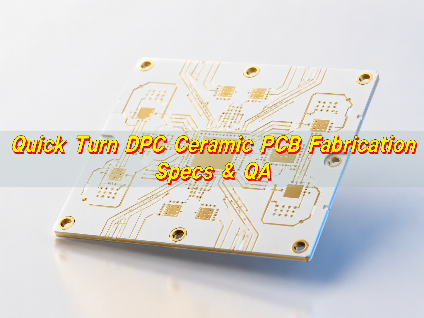
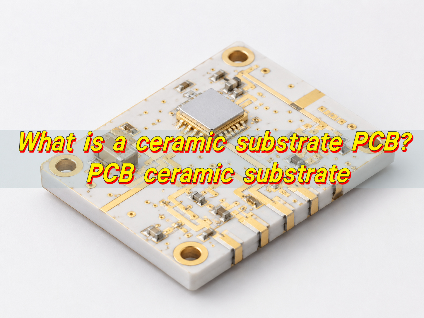
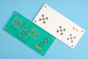
What Is a Ceramic PCB for RF?
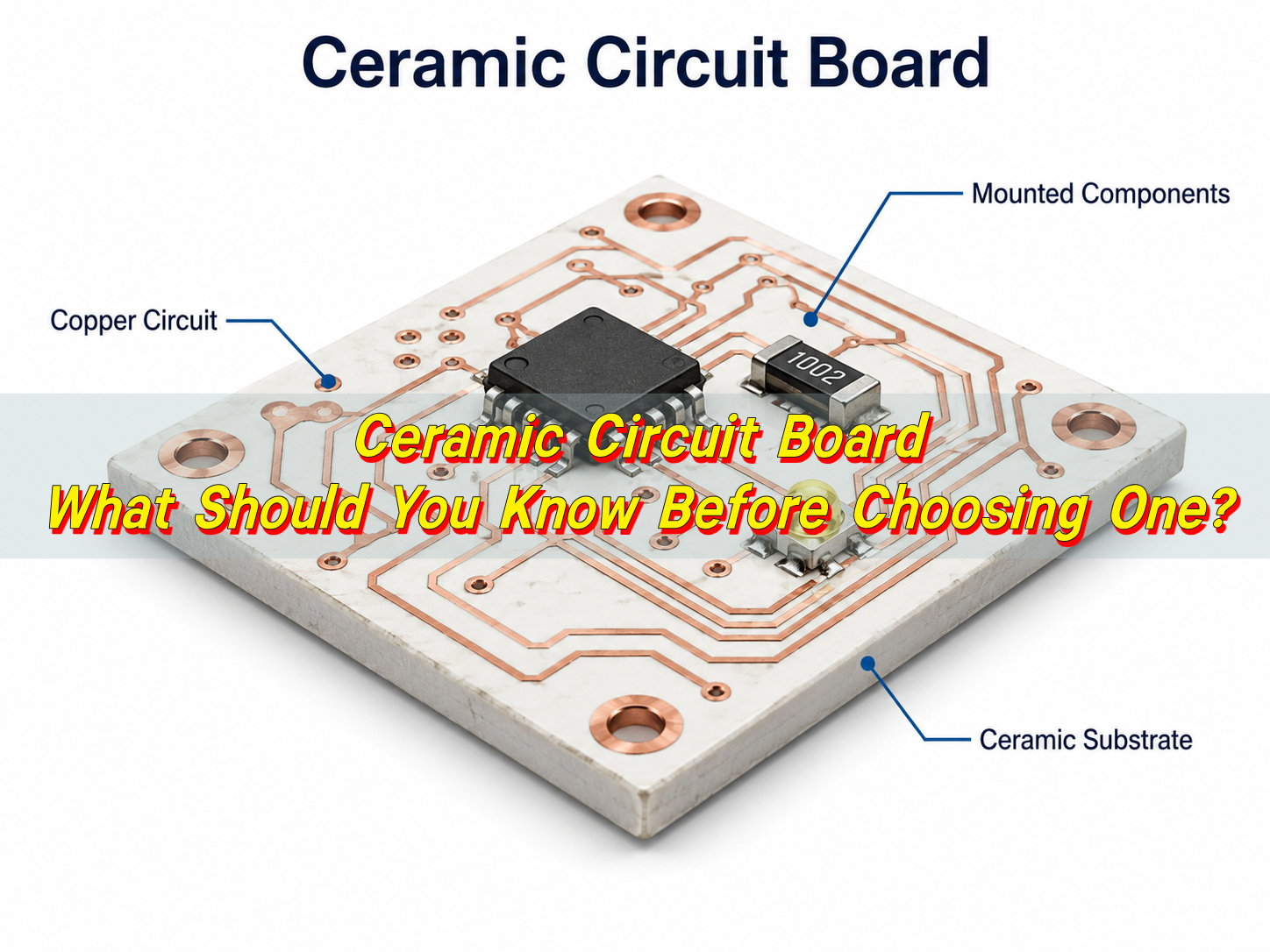
A ceramic PCB for RF is a circuit board or substrate used in high-frequency circuits where dielectric stability, low signal loss, dimensional accuracy, and thermal reliability matter more than standard PCB cost.
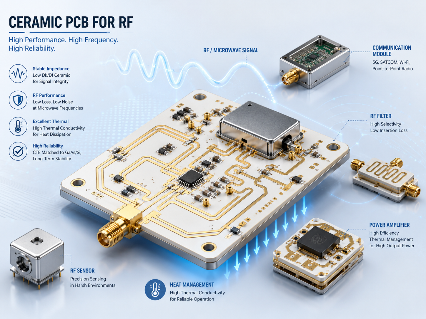
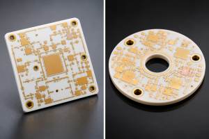
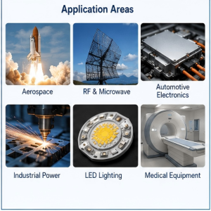
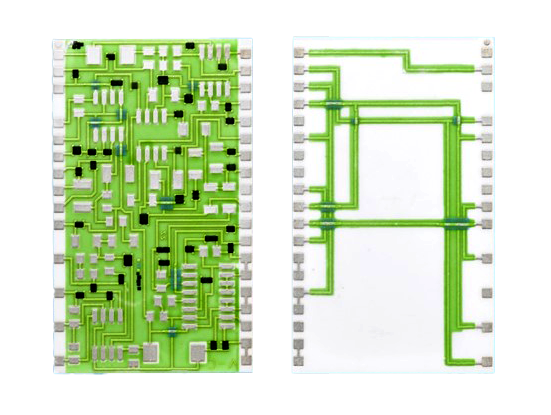
In RF and microwave applications, the substrate is part of the electrical design. It affects impedance, insertion loss, resonance behavior, signal phase, and long-term stability. This is why engineers often consider ceramic PCB substrate options such as alumina PCB for RF modules, microwave circuits, filters, sensors, power amplifiers, and hybrid circuits.
Why Ceramic PCB Substrate Matters in RF Circuits?
A ceramic PCB substrate matters in RF circuits because high-frequency signals are sensitive to material behavior. Small changes in dielectric constant, trace geometry, surface quality, or substrate thickness can shift impedance and affect performance.
For buyers, the key point is simple: RF ceramic PCB is not selected only for heat dissipation. The material must support stable signal behavior at the target frequency. A supplier must understand both ceramic PCB manufacturing and the RF requirements behind the drawing.
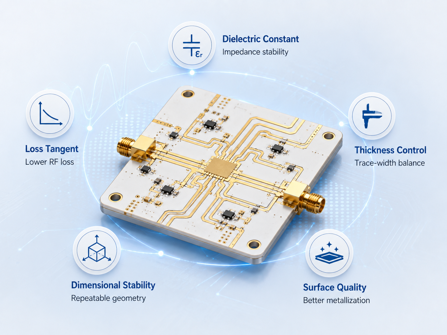
Key RF Properties: Dielectric Constant, Loss Tangent, and Dimensional Stability
For RF ceramic PCB projects, three material properties usually matter most: dielectric constant, loss tangent, and dimensional stability.
| RF Property | Why It Matters | Buyer Note |
|---|---|---|
| Dielectric constant | Affects impedance, wavelength, trace width, and circuit size | Confirm the value required by the RF design, not only the material name |
| Loss tangent | Affects signal loss at high frequency | Lower loss is more important as frequency increases |
| Substrate thickness | Affects impedance and manufacturable line width | Keep thickness controlled and clearly specified |
| Dimensional stability | Helps maintain trace geometry and circuit repeatability | Important for filters, antennas, resonators, and microwave circuits |
| Surface quality | Affects metallization and high-frequency current behavior | Review finish and metallization process early |
A good RF ceramic PCB quote should not start with “Can you make ceramic PCB?” It should start with frequency range, impedance target, material requirement, line width, tolerance, and metallization needs.
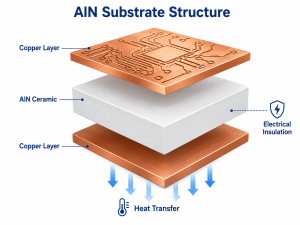
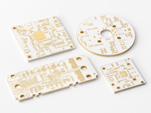
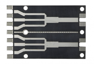
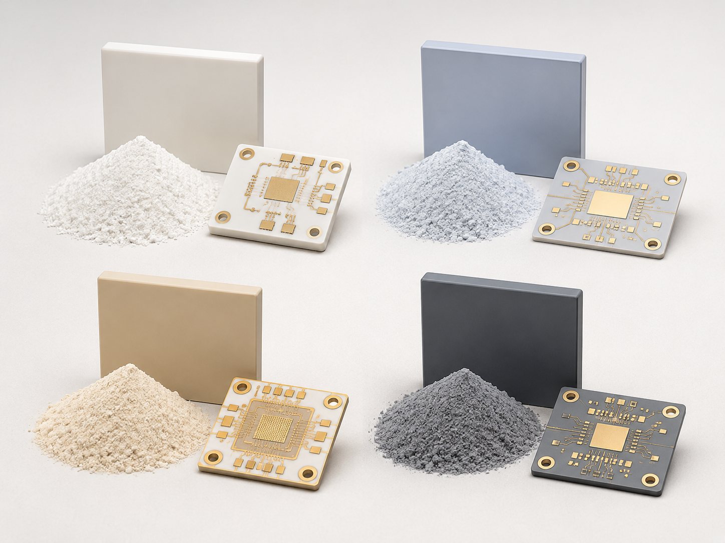
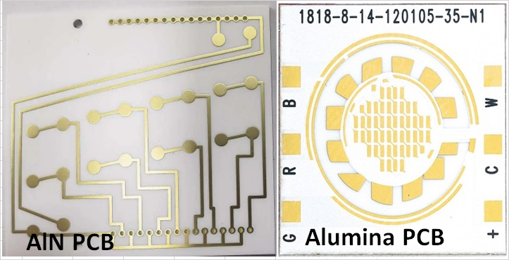
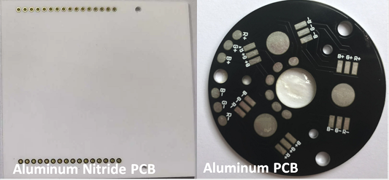
Common Materials: Alumina PCB, AlN, Rogers, and FR4
Material choice depends on frequency, loss target, thermal demand, cost, and manufacturing method. Alumina PCB is common in RF ceramic substrate applications, but it is not the only option.
| Material | RF Strength | Limitation | Best Use |
|---|---|---|---|
| Alumina PCB | Stable ceramic substrate, good mechanical and thermal behavior, widely used in RF and hybrid circuits | Higher dielectric constant than many organic RF laminates; design must account for it | RF modules, microwave circuits, sensors, hybrid circuits |
| Aluminum nitride PCB | Better thermal conductivity than alumina | Higher cost; not always needed for RF unless heat is also a major issue | RF power modules, high-power microwave circuits, compact thermal designs |
| Rogers / PTFE-based RF laminate | Common for RF PCB design, lower-loss options available | Material and processing cost can be higher than FR4; thermal/mechanical behavior differs from ceramic | Antennas, RF boards, microwave circuits, communication devices |
| FR4 | Low cost and easy to manufacture | Loss and dielectric variation become problematic at higher frequencies | Low-frequency or cost-sensitive circuits where RF loss is acceptable |
For many RF ceramic PCB projects, alumina PCB is selected when the design needs ceramic stability, precision metallization, and reliable high-frequency behavior in a compact substrate.
Ceramic PCB for RF vs Standard RF PCB Materials
The decision between ceramic PCB and standard RF laminate depends on circuit function, frequency, power level, size, and reliability environment.
| Option | Advantage | Limitation | Better Fit |
|---|---|---|---|
| Ceramic PCB for RF | Stable substrate, good thermal behavior, suitable for hybrid and precision circuits | Higher cost and stricter manufacturing limits | RF modules, microwave packages, high-stability circuits |
| Rogers RF PCB | Mature RF laminate option with known dielectric choices | Not ceramic; thermal and mechanical behavior differ | Antennas, RF communication boards, microwave PCB layouts |
| FR4 RF design | Low cost and fast production | Higher loss and less predictable dielectric behavior at high frequency | Low-frequency RF, simple prototypes, cost-sensitive products |
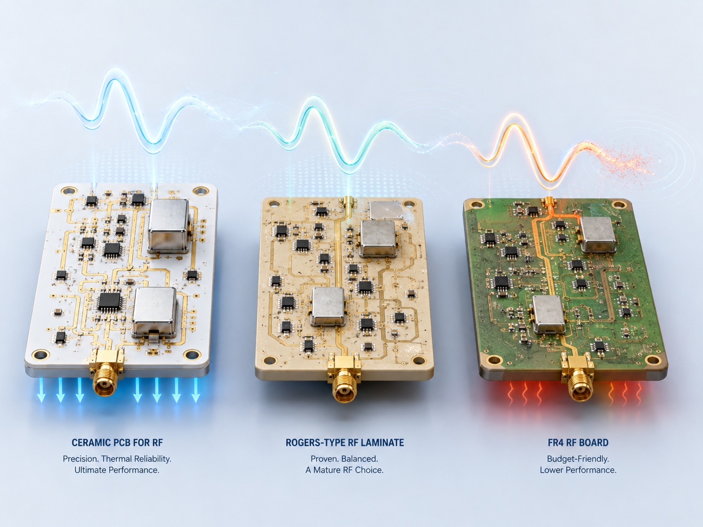
The practical takeaway: use FR4 only when RF loss and dielectric variation are acceptable. Use Rogers-type RF laminates for many standard RF boards. Use ceramic PCB when the design needs ceramic stability, compact structure, precision, or stronger thermal reliability.
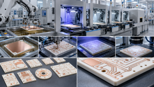
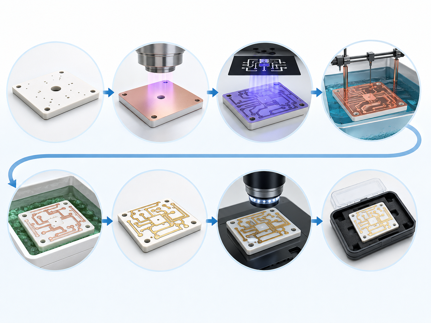
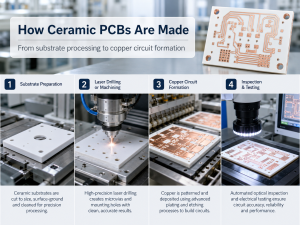
Ceramic PCB Manufacturing Considerations for RF Applications
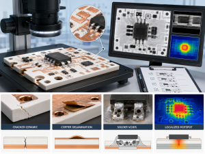
Ceramic PCB manufacturing for RF applications must control the details that affect signal performance. A small trace width error may be more serious in RF than in a normal power or control PCB.
Important manufacturing points include:
- Substrate material and thickness control
- Fine line and spacing capability
- Metallization method, such as thick film, thin film, DBC, or other suitable process
- Copper or conductor thickness
- Surface roughness and finish
- Dimensional tolerance
- Via and hole quality if required
- Flatness and warpage
- Pattern registration
- Cleanliness and handling
For RF ceramic PCB manufacturing, the supplier should review whether the requested geometry is manufacturable before production. If the layout uses very fine traces, tight impedance targets, or microwave structures, early engineering communication reduces prototype failure risk.
When Should You Choose Alumina PCB for RF?
Choose alumina PCB for RF when the circuit needs a stable ceramic substrate, good dimensional control, and reliable behavior in a compact or harsh environment.
Alumina PCB is often suitable for:
- RF hybrid circuits
- Microwave modules
- Sensor circuits
- Thin film or thick film RF substrates
- Filters and matching networks
- High-temperature or high-reliability electronics
- Compact modules where ceramic stability is useful
Alumina may be unnecessary if the circuit can meet RF performance with a standard RF laminate at lower cost. It may also be the wrong choice if the design requires a different dielectric constant, lower loss material, or stronger thermal conductivity than alumina can provide.
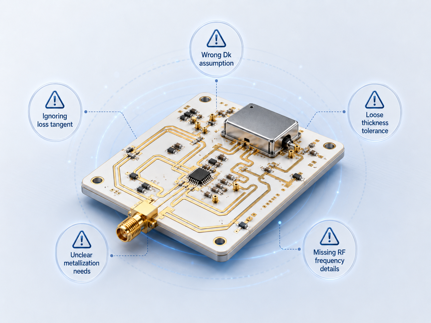
Common Design and Purchasing Mistakes
The most common mistake is treating RF ceramic PCB like a normal ceramic circuit board. RF performance depends on both material and geometry.
| Mistake | Why It Causes Problems | Better Approach |
|---|---|---|
| Only asking for “ceramic PCB for RF” | Supplier cannot confirm material, frequency, or process | Provide frequency range, substrate material, and circuit function |
| Ignoring dielectric constant | Impedance and trace width may shift | Specify target dielectric constant or approved material |
| Ignoring loss tangent | High-frequency loss may become unacceptable | Define frequency and acceptable RF performance |
| Using vague tolerances | RF traces may not match design intent | Specify line width, spacing, substrate thickness, and dimensional tolerance |
| Choosing alumina automatically | Alumina may not fit every RF design | Compare alumina, AlN, Rogers, and FR4 based on real requirements |
| Sending only Gerbers | Supplier cannot judge RF function or risk | Include stackup, material notes, impedance targets, and application context |
A good ceramic PCB manufacturer should ask technical questions before quotation if the RF requirements are unclear.
How to Choose a Ceramic PCB Manufacturer for RF Projects?
A ceramic PCB manufacturer for RF projects should be evaluated by engineering communication, material control, metallization capability, and tolerance control, not only by price.
Useful supplier checks include:
- Experience with RF or microwave ceramic substrate projects
- Ability to manufacture alumina PCB and other ceramic PCB substrate types
- Clear process options for thin film, thick film, or metallized ceramic circuits
- Fine line and spacing capability
- Substrate thickness and dimensional tolerance control
- Inspection process for metallization, surface finish, and pattern accuracy
- Willingness to review drawings before quoting
- Ability to support prototypes before mass production
- Clear communication about manufacturing limits and alternatives
For EBest Circuit (Best Technology), RF ceramic PCB review should focus on whether the drawing, material, tolerance, and production method match the actual frequency and application requirement.
What to Provide When Requesting an RF Ceramic PCB Quote
A complete RFQ helps the supplier evaluate manufacturability, cost, and performance risk before production.
Provide these details when requesting a ceramic PCB quote:
- Application type, such as RF module, microwave circuit, sensor, or power amplifier
- Frequency range
- Ceramic material preference, such as alumina PCB or AlN
- Required dielectric constant if specified
- Loss requirement if specified
- Substrate dimensions and thickness
- Line width and spacing
- Metallization method or conductor requirement
- Copper or metal thickness
- Surface finish
- Hole, via, or edge requirements
- Dimensional tolerance
- Quantity for prototype and mass production
- Test or inspection requirements
- Gerber files, drawings, and stackup notes
If the project is still in early design, provide the target frequency, operating environment, and performance concern. This allows the ceramic PCB manufacturer to suggest practical material and process options before the design is locked.
FAQ
Is ceramic PCB good for RF?
Yes. Ceramic PCB can be good for RF when the circuit needs dielectric stability, dimensional accuracy, thermal reliability, and compact substrate design. It is especially useful for RF modules, microwave circuits, hybrid circuits, sensors, and high-reliability electronics.
Why is alumina PCB used in RF circuits?
Alumina PCB is used in RF circuits because it provides a stable ceramic substrate, good mechanical strength, useful thermal behavior, and compatibility with thin film or thick film metallization. It is common in RF and microwave hybrid circuits.
Is ceramic PCB better than Rogers PCB for RF?
Not always. Rogers-type RF laminates are widely used for RF PCB designs, antennas, and microwave boards. Ceramic PCB is better when the design needs ceramic stability, compact substrate behavior, precision metallization, or stronger thermal/mechanical reliability.
Can FR4 be used for RF circuits?
FR4 can be used for lower-frequency or cost-sensitive RF circuits, but it becomes less predictable as frequency increases. Loss, dielectric variation, and tolerance control can limit performance in higher-frequency RF designs.
What affects RF performance in ceramic PCB manufacturing?
RF performance can be affected by dielectric constant, loss tangent, substrate thickness, line width, spacing, metallization quality, surface roughness, dimensional tolerance, and pattern registration.
What is the difference between alumina PCB and AlN PCB for RF?
Alumina PCB is commonly used for RF ceramic substrates and is usually more cost-effective. AlN PCB offers higher thermal conductivity, so it is useful when the RF circuit also has significant heat dissipation requirements.
What should I ask a ceramic PCB manufacturer before ordering?
Ask about material options, RF project experience, fine line capability, metallization process, substrate thickness tolerance, dimensional tolerance, inspection method, prototype support, and whether they can review RF-related drawing requirements before production.
Do I need impedance control for ceramic PCB for RF?
Many RF ceramic PCB designs need impedance awareness, even if the supplier does not provide full RF simulation. At minimum, the buyer should provide frequency range, trace geometry, substrate thickness, dielectric requirement, and critical RF areas.
Conclusion
A ceramic PCB for RF is not just a ceramic version of a normal PCB. The substrate affects impedance, signal loss, circuit size, stability, and long-term performance. Alumina PCB is often a practical RF ceramic substrate, while AlN, Rogers materials, and FR4 each fit different design conditions.
If you are evaluating ceramic PCB substrate options, alumina PCB, ceramic PCB manufacturing, or RF PCB prototype support, EBest Circuit (Best Technology) can help review your drawings, material requirements, tolerance needs, and quotation details. Contact us at sales@bestpcbs.com.