A Yagi PCB antenna uses printed conductive elements to concentrate RF energy in a specific direction. Its performance depends on element dimensions, PCB materials, feed structure, and impedance matching. Small changes in these factors can shift the resonant frequency, reduce gain, or distort the radiation pattern.
For a 2.4 GHz Yagi PCB antenna, good impedance matching alone is not enough. The antenna must also deliver the required directional performance. This guide covers practical design parameters, dimensions, 50 Ω matching, simulation, and testing methods.
What Is a Yagi PCB Antenna and How Does It Work?
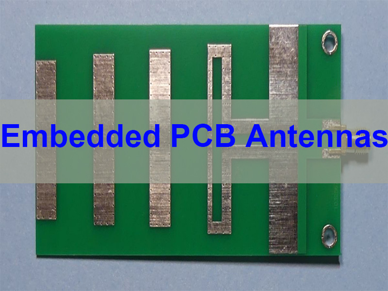
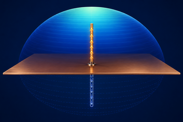
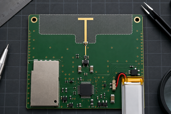
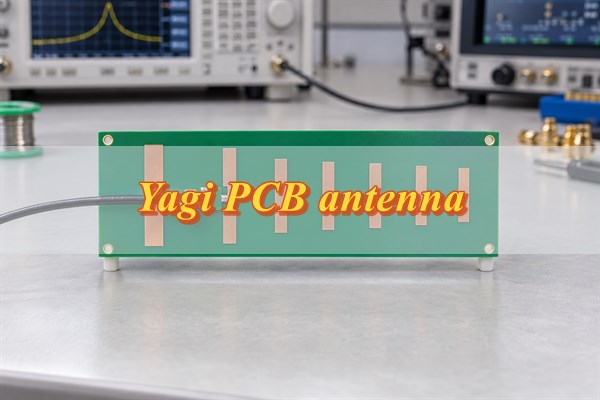
A Yagi PCB antenna is a printed version of the Yagi‑Uda antenna. It uses copper patterns on a PCB instead of separate metal rods. A driven element and surrounding parasitic elements interact through electromagnetic coupling to produce directional radiation.
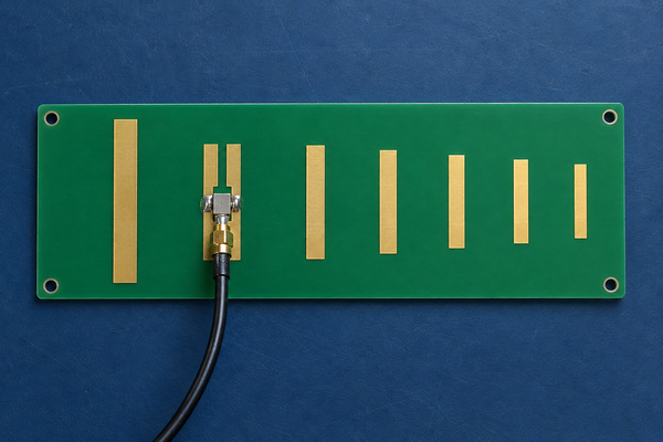
A typical printed Yagi‑Uda antenna contains three types of elements:
- Driven Element: Connects to the RF feed and generates or receives electromagnetic signals. A printed dipole is a common configuration.
- Reflector: Positioned behind the driven element to reduce backward radiation and help shape the forward beam.
- Directors: Placed in front of the driven element to concentrate radiation toward the desired direction.
The reflector and directors have no direct electrical connection to the feed. Instead, currents induced by the driven element alter the combined radiation pattern.
This directional characteristic makes the antenna suitable for fixed wireless links, directional Wi‑Fi coverage, and point‑to‑point communication where the signal direction is known.
What Design Parameters Should You Define for a Yagi PCB Antenna?
Before designing a Yagi PCB antenna, define the operating frequency, required gain, directional coverage, PCB size, and feed conditions. These parameters establish the targets for element sizing, impedance matching, and performance testing.
| Parameter | Design Requirement |
|---|---|
| Operating Frequency | Target frequency and operating range, such as 2.4 GHz |
| Bandwidth | Frequency range meeting matching and radiation requirements |
| Target Gain | Minimum forward gain (dBi) across the required band |
| Beamwidth & Front‑to‑Back Ratio | Required beam coverage and rejection of backward radiation |
| Radiation Efficiency | Minimum acceptable efficiency (%) across the operating band |
| PCB Dimensions | Available antenna length, width, and copper clearance |
| Polarization | Required polarization and antenna orientation |
| Feed Interface | Typically 50 Ω, with an appropriate balanced or unbalanced feed |
| Stackup Constraints | Available layers, substrate thickness, and material limitations |
| Installation Environment | Enclosure, mounting position, nearby metal, and cable routing |
Gain, bandwidth, beamwidth, and PCB size are interdependent. Their targets should be considered together before finalizing the antenna geometry.
Which PCB Materials and Stackups Are Suitable for a Yagi PCB Antenna?
FR-4 works for many 2.4 GHz Yagi PCB antenna designs, particularly where material cost matters. Low‑loss RF laminates can improve efficiency and dielectric consistency, although their benefits depend on the antenna geometry and operating frequency.
| Property | FR-4 | Low‑Loss RF Laminate |
|---|---|---|
| Material Cost | Generally lower | Generally higher |
| Dielectric Loss | Usually higher | Usually lower |
| Dk Consistency | Varies by laminate grade | Often more tightly controlled |
| RF Performance | Suitable for many moderate‑frequency applications | Better suited to loss‑sensitive RF designs |
| Material Selection | Check Dk and Df at the operating frequency | Check Dk, Df, thickness, and availability |
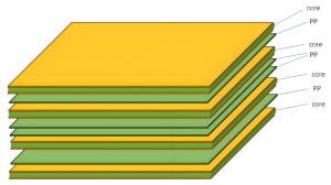
For printed antennas, material selection affects both the radiating elements and the transmission‑line structure. The following stackup characteristics deserve attention:
- Dielectric Constant (Dk): Influences electrical length, resonance, and feed impedance.
- Dissipation Factor (Df): Contributes to dielectric loss and affects radiation efficiency.
- Layer Spacing: Affects coupling between conductors and the characteristics of multilayer feed structures.
- Copper Thickness: Influences conductor loss and the final etched geometry.
- Ground Plane Layout: Can act as a reflector or disturb radiation if placed incorrectly.
A practical example is the Texas Instruments DN034 Yagi antenna, built on a 1.6 mm, four‑layer FR-4 PCB. Its antenna conductors use two adjacent layers separated by approximately 0.226 mm.
In that layout, the ground plane serves as the reflector, while the driven element and directors follow a defined copper pattern. Routing beneath the antenna is restricted on specified layers to preserve its behavior.
The total PCB thickness and the spacing between antenna conductor layers are different parameters. Both must be checked when adapting an existing layout to another stackup.
How Do You Calculate Yagi PCB Antenna Dimensions for 2.4 GHz?
Yagi PCB antenna dimensions start with the operating wavelength, but the final printed element lengths depend on substrate properties, conductor geometry, and coupling between elements.
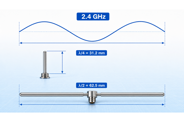
The free‑space wavelength is calculated as:
λ₀ = c / f
Where:
- λ₀: Free‑space wavelength
- c: Speed of light, approximately 3 × 10⁸ m/s
- f: Operating frequency in Hz
For 2.4 GHz:
λ₀ = (3 × 10⁸) / (2.4 × 10⁹) = 125 mm
A free‑space half‑wavelength is therefore 62.5 mm. This is a useful starting reference, not a universal printed dipole length.
The following dimensions come from the Texas Instruments DN034 reference design.
| Dimension | Reference Value |
|---|---|
| Reference PCB Size | 100 × 150 mm |
| Driven Element Length (L2) | 44.96 mm |
| Director Length (L3–L5) | 34.29 mm |
| Reflector‑to‑Driven Spacing (S12) | 16.00 mm |
| Driven‑to‑Director Spacing (S23) | 15.49 mm |
| Director Spacing (S34, S45) | 15.49 mm |
| Driven Element Width (W2) | 3.05 mm |
| Director Width (W3–W5) | 3.81 mm |
| End Clearance (S56) | 36.20 mm |
These dimensions belong to a specific antenna geometry, including its ground‑plane reflector, integrated balun, PCB stackup, and surrounding board area. They are not interchangeable design rules for other substrates or layouts.
The main dimensional relationships are:
- Driven Element Length: Strongly affects resonance and input impedance.
- Reflector Geometry: Influences backward radiation and front‑to‑back ratio.
- Director Length and Spacing: Influence forward gain, beam shape, and mutual coupling.
- Conductor Width: Affects impedance and current distribution.
- PCB Edge Clearance: Can alter radiation behavior when the board outline changes.
For a new design, calculate the initial dimensions, model the complete antenna geometry, and adjust the elements through electromagnetic simulation. Do not scale individual dimensions independently of the feed and reflector structure.
How Do You Achieve 50 Ω Impedance Matching in a Yagi PCB Antenna?
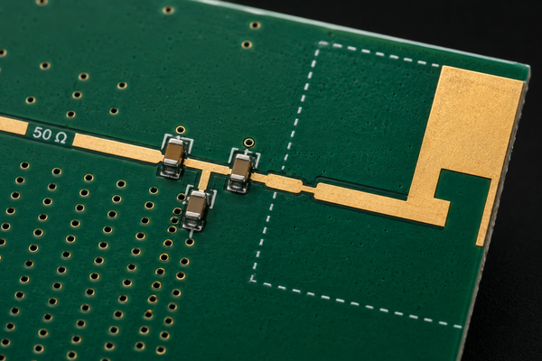
Yagi PCB antenna impedance matching minimizes signal reflection between the antenna and the RF system. Because many transceivers use a 50 Ω interface, the antenna’s complex input impedance must be transformed to provide an acceptable match across the operating band.
The matching method depends on the antenna topology and its feed structure.
- Feed Geometry: Adjust the feed connection or geometry where the antenna design allows it.
- Balun: Convert an unbalanced feed into a balanced feed when driving a printed dipole.
- Transmission‑Line Matching: Use an appropriate line geometry or impedance‑transforming section.
- Matching Network: Add RF inductors or capacitors to correct the remaining mismatch.
- Smith Chart: Identify the measured complex impedance and determine the required transformation.
A printed dipole is a balanced radiator, while a conventional microstrip feed is unbalanced. The TI DN034 design uses a tapered printed balun to connect a 50 Ω microstrip input to a balanced two‑wire dipole feed.
For designs that include a matching network, the adjustment process is straightforward.
Step 1: Measure or simulate the antenna input impedance across the required frequency range.
Step 2: Check the feed transition and antenna geometry before adding matching components. A layout problem may not be solved by component tuning alone.
Step 3: Use the Smith Chart to select a suitable matching topology and calculate initial component values.
Step 4: Adjust the network using RF‑rated components and repeat the impedance measurement.
The TI reference design also recommends allowing space for a π-matching network near the antenna feed. This provides tuning flexibility when changes in PCB construction or nearby objects cause detuning. If matching components are unnecessary, the series position can be populated appropriately and unused shunt positions left unpopulated.
A good 50 Ω match reduces reflected power but does not guarantee high radiation efficiency or forward gain. Those characteristics depend on the complete antenna structure.
What Do Gain and Radiation Patterns Reveal About Antenna Performance?
Yagi PCB antenna gain indicates the strength of radiation in a particular direction, while the radiation pattern shows how that energy is distributed in space. Higher forward gain is useful for directional links, but it often comes with a narrower beam.
Several measurements describe directional performance:
- Gain (dBi): Directional radiation performance, including radiation efficiency.
- Directivity: Radiation concentration without accounting for antenna losses.
- Beamwidth: Angular width of the main beam, usually measured at the half‑power points.
- Front‑to‑Back Ratio: Comparison of forward and opposite‑direction radiation.
- Side Lobes: Secondary radiation peaks outside the main beam.
The following measurements from TI’s DN034 antenna show why gain and efficiency must be considered separately.
| Frequency | Gain | Directivity | Efficiency |
|---|---|---|---|
| 2400 MHz | 7.22 dBi | 7.92 dBi | 85.20% |
| 2440 MHz | 7.18 dBi | 8.62 dBi | 71.70% |
| 2480 MHz | 7.13 dBi | 9.48 dBi | 58.24% |
Published measurements for the TI DN034 reference design.
Although peak gain remains close to 7.2 dBi, radiation efficiency falls from 85.20% to 58.24%. Increasing directivity offsets much of that efficiency reduction in the reported gain.
This distinction matters because a Yagi PCB antenna can maintain similar peak gain while its total radiated performance changes considerably across the band.
For a fixed wireless link, examine gain, beamwidth, front‑to‑back ratio, and efficiency across the actual operating frequencies, not just the highest advertised gain.
How Do You Simulate and Optimize a Yagi PCB Antenna?
Electromagnetic simulation helps predict resonance, impedance, gain, and radiation patterns before PCB fabrication. Ansys HFSS and CST Studio Suite are commonly used for this type of antenna analysis.
A practical simulation workflow follows five steps.
Step 1: Build the Antenna Model
Include the driven element, reflector, directors, feed structure, and PCB stackup. Use material properties specified for the operating frequency.
Step 2: Set the Simulation Conditions
Define the frequency sweep, excitation port, and radiation boundaries. Include nearby ground structures or enclosure features that may affect antenna behavior.
Step 3: Check Initial Performance
Review S11, input impedance, gain, radiation efficiency, and radiation pattern. Identify which results fail to meet the design targets.
Step 4: Adjust the Geometry
Change driven element dimensions to investigate resonance shifts. Tune director lengths and spacing to improve directional performance. Refine the feed structure to improve impedance matching.
Step 5: Verify the Design
Recheck matching, gain, and radiation patterns across the operating band. Test the design’s sensitivity to realistic dielectric‑property and manufacturing variations.
For example, shortening a driven element may move resonance upward in frequency, but it can also alter coupling and impedance. Every geometry adjustment should be evaluated against the full antenna performance, not just one S11 point.
How Do You Test S11, Return Loss, and VSWR?
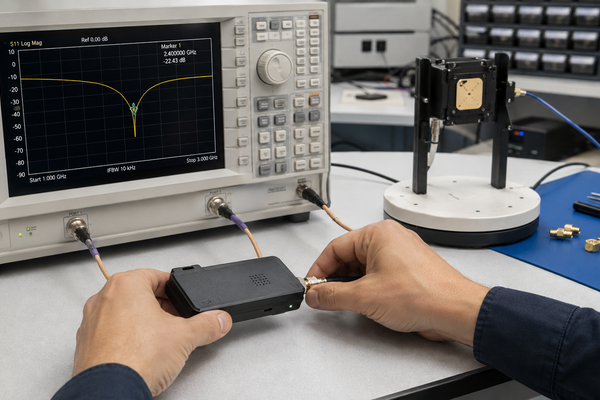
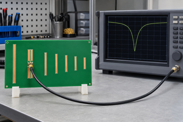
Yagi PCB antenna testing usually begins with a vector network analyzer (VNA) to measure input reflection across the operating band. S11, return loss, and VSWR describe the same reflection behavior in different forms.
The relationship between these measurements is:
| S11 | Return Loss | VSWR | Reflected Power |
|---|---|---|---|
| −6 dB | 6 dB | 3.01:1 | 25.12% |
| −10 dB | 10 dB | 1.92:1 | 10.00% |
| −15 dB | 15 dB | 1.43:1 | 3.16% |
| −20 dB | 20 dB | 1.22:1 | 1.00% |
S11 ≤ −10 dB is a common matching criterion, although the required limit depends on the RF system. At exactly −10 dB, 10% of incident power is reflected and approximately 90% is accepted at the measured port.
The measurement procedure is:
Step 1: Calibrate the VNA across the intended frequency range and establish an appropriate measurement reference plane.
Step 2: Connect the antenna through a suitable RF connector or test fixture. Keep the measurement cable away from the radiating elements where practical.
Step 3: Measure S11 over a frequency span that includes the complete operating band and enough margin to identify resonance shifts.
Step 4: Check the Smith Chart and determine the bandwidth meeting the specified reflection limit.
Step 5: Compare the measured results with the simulated impedance and matching bandwidth.
In the TI DN034 reference design, the measured −10 dB S11 bandwidth is approximately 497 MHz, extending from 2126 MHz to 2623 MHz. Its input match also remains within approximately 1.4:1 VSWR at the reported 2.4 GHz test frequencies.
These figures demonstrate a broad impedance match for that specific antenna. Matching bandwidth should not be confused with the frequency range over which radiation performance satisfies the application requirements.
How Do You Measure Yagi PCB Antenna Gain and Radiation Pattern?
Gain and radiation patterns require over‑the‑air (OTA) testing. Unlike VNA measurements, which examine reflected RF power at the feed, OTA measurements evaluate radiation through space.
An antenna measurement range or anechoic chamber can provide controlled conditions for these tests.
- Gain Measurement: Compare the antenna under test with a calibrated reference antenna to establish directional gain.
- Radiation Pattern Measurement: Rotate the antenna or measurement system to record radiation at different angles.
- E‑Plane and H‑Plane Measurements: Examine principal‑plane radiation characteristics, including beamwidth and unwanted lobes.
- Front‑to‑Back Ratio: Compare forward radiation with radiation in the opposite direction.
- Radiation Efficiency: Use a suitable calibrated measurement method to determine the portion of accepted RF power that is radiated.
Conventional far‑field measurements require adequate separation between the antenna and measurement equipment. Alternatively, a validated near‑field measurement system can be used with the appropriate field transformation.
During testing, control polarization alignment, RF cable routing, fixture position, and environmental reflections. These factors can change measured patterns, particularly when the antenna has a narrow main beam.
For a 2.4 GHz Yagi PCB antenna, measuring at 2400 MHz, 2440 MHz, and 2480 MHz provides useful checkpoints across the band, as demonstrated by the TI reference design.
If the final product includes an enclosure or nearby metal structure, repeat relevant measurements in that configuration. The radiation pattern of an exposed prototype may differ from that of the finished product.
Why Do Yagi PCB Antenna Test Results Differ from Simulation?
Differences between simulation and testing usually involve material properties, fabricated dimensions, feed transitions, or the measurement environment. The observed problem helps identify where to start checking.
| Test Problem | Possible Cause | Recommended Check |
|---|---|---|
| Resonance Shift | Dk variation or element dimension error | Verify laminate properties and fabricated geometry |
| Poor S11 | Feed mismatch, connector transition, or coupling changes | Check calibration, feed dimensions, and input impedance |
| Lower Gain | Material loss, cable coupling, or measurement error | Check substrate losses and OTA measurement conditions |
| Distorted Radiation Pattern | Metal objects, mounting fixtures, or RF cables | Repeat measurements with controlled surroundings |
| Unexpected Bandwidth | Stackup or geometry differences | Compare actual PCB dimensions and materials with the model |
Start with the discrepancy that is easiest to isolate. If the resonant frequency has shifted, inspect the substrate and element dimensions before changing matching components. If S11 agrees with simulation but measured gain is lower, investigate losses and the OTA setup.
Change one parameter at a time and repeat the relevant measurement. This makes it possible to identify whether the correction improved the antenna or merely shifted the problem elsewhere.
FAQs About Yagi PCB Antennas
Q1: Can a Yagi PCB antenna be integrated into the main circuit board?
A1: Yes. A Yagi PCB antenna can share a board with other electronic circuits if the required radiating area, feed structure, and copper clearances are preserved. Nearby components and copper can change the antenna’s performance, so the complete PCB assembly should be evaluated.
Q2: Does solder mask affect Yagi PCB antenna performance?
A2: Yes. Solder mask introduces additional dielectric material around printed conductors, potentially shifting resonance or impedance. The effect depends on mask thickness, dielectric properties, and coverage. Use the intended solder mask configuration during simulation and testing.
Q3: Can a Yagi PCB antenna operate inside a plastic enclosure?
A3: Yes, but plastic can alter resonance and radiation characteristics. The effect depends on the material’s dielectric properties and its distance from the antenna. Test the antenna inside the final enclosure before approving its performance.
Q4: Can the same antenna layout work at different frequencies?
A4: Not necessarily. Yagi antenna dimensions are related to wavelength and the coupling between elements. A design optimized for 2.4 GHz will not automatically perform well at 5 GHz. A major frequency change generally requires redesign or scaling followed by retuning.
Q5: What happens if the PCB outline is trimmed near the antenna?
A5: Reducing the surrounding PCB area may change fringing fields, reflector behavior, and radiation characteristics. This is particularly relevant when copying an existing reference design. Preserve the specified board outline and edge clearances unless the modified geometry has been verified.
Q6: How does RF cable placement affect antenna performance?
A6: An RF cable can couple to the antenna and introduce unwanted common‑mode currents, changing impedance or radiation patterns. Keep cable routing consistent and use appropriate feed isolation during measurements, especially when comparing results with simulation.
Q7: Can a fabricated Yagi PCB antenna be tuned?
A7: Some impedance errors can be corrected using a suitable matching network. However, problems caused by incorrect element dimensions or unsuitable radiation patterns may require a PCB revision. Improving S11 does not always correct low gain or poor directivity.
Q8: Are Yagi PCB antennas suitable for moving wireless devices?
A8: They can be used when the direction of communication remains known or the antenna can be aligned. For devices whose orientation changes unpredictably, a directional beam may cause inconsistent coverage. Omnidirectional antennas are often more practical when all‑around coverage is required.
Q9: Which PCB manufacturing tolerances matter for a printed Yagi antenna?
A9: Element width, spacing, copper geometry, layer registration, and dielectric thickness can affect the final RF characteristics. Their influence depends on the antenna design. Fabrication tolerances should be checked against the validated geometry, particularly around the driven element and feed transition.
Q10: Can a Yagi PCB antenna transmit and receive signals?
A10: Yes. A conventional passive Yagi antenna is reciprocal, so its directional characteristics apply to both transmitting and receiving under corresponding conditions. Frequency range, impedance matching, polarization, and antenna orientation remain relevant in both modes.
Conclusion
A Yagi PCB antenna achieves directional radiation through carefully arranged driven and parasitic elements. Its performance depends on geometry, PCB materials, feed construction, and 50 Ω impedance matching. Wavelength calculations provide initial dimensions, while electromagnetic simulation and prototype testing establish the final design. VNA measurements confirm input matching; OTA testing verifies gain, radiation patterns, and efficiency.
For Yagi PCB antenna fabrication, EBest Circuit provides PCB manufacturing, assembly, and DFM review based on customer‑supplied designs. Our team can review stackups, copper geometry, dimensional tolerances, and manufacturing feasibility before prototype or volume production. Contact sales@bestpcbs.com with your PCB files and requirements for technical review and a quotation.