





High-density PCB prototypes are different from standard FR4 prototype boards. A simple board may only need basic fabrication checks, but a high-density prototype can involve HDI structures, fine line/space, microvias, buried vias, controlled impedance, BGA via-in-pad, heavy copper, thin dielectric layers, or tight assembly requirements. For buyers comparing the best manufacturers high-density PCB prototypes USA projects may require, the real question is whether the supplier can review these risks before production starts.
For USA engineering teams, choosing a manufacturer is not only about price or location. As a quick turn HDI PCB prototype manufacturer, EBest Circuit (Best Technology) supports custom PCB fabrication, HDI PCB manufacturing, stackup review, DFM checking, component sourcing, SMT assembly, testing, and small-batch production. If your project includes HDI structure, impedance notes, BGA areas, special material, or urgent prototype validation, send your Gerber files, stackup drawing, BOM, assembly notes, or questions to sales@bestpcbs.com for engineering review.

How to Compare Manufacturers for High-Density PCB Prototypes in the USA?
When engineers search for the best manufacturers for high-density PCB prototypes in the USA, the useful question is not “Which company is the biggest?” It is “Which supplier can handle this prototype without creating hidden risk?”
For simple 2-layer or 4-layer boards, many online prototype platforms may be enough. For high-density PCB prototypes, compare manufacturers by practical project fit:
- HDI capability, not only standard through-hole multi-layer PCB
- Blind via, buried via, laser via, and via-in-pad review
- Stackup review before production
- Controlled impedance support and test reports
- BGA routing and soldering risk control
- Resin-filled and plated-over via capability
- Prototype-to-small-batch production support
- PCB fabrication plus PCBA assembly if SMT is required
- Clear communication before EQ, production files, or stackup changes
A USA buyer may choose a domestic manufacturer for local communication, special compliance needs, or extremely short domestic logistics. Many USA engineering teams also work with overseas manufacturers when the project needs HDI capability, cost control, flexible small-batch production, and one-stop PCB plus PCBA support.
Best Manufacturers High-Density PCB Prototypes USA
When buyers search for the best manufacturers high-density PCB prototypes USA, they are usually comparing more than company names. The real decision is which supplier fits the board complexity, delivery pressure, quality requirement, and next-stage production plan.
Sierra Circuits (California, USA)
- Main Business: Quick-turn PCB prototypes, HDI boards, PCB assembly.
- Strength: Strong for U.S.-based prototype builds, DFM support, HDI, microvias, via-in-pad, and controlled impedance projects.
- Best Fit: Engineering teams that need fast domestic prototype fabrication and assembly.
- Check Before Ordering: Confirm HDI stackup, microvia structure, impedance report, IPC class, and assembly scope.
AdvancedPCB (USA)
- Main Business: Quick-turn PCB fabrication, HDI, UHDI, flex, rigid-flex, and assembly.
- Strength: Good for engineers who need fast U.S. prototype support with CAM review and flexible turnaround options.
- Best Fit: R&D teams working on HDI prototypes, multilayer boards, or urgent design validation.
- Check Before Ordering: Confirm whether the job is standard technology, HDI, or advanced technology, because lead time and cost can change quickly.
Summit Interconnect (USA)
- Main Business: Complex rigid PCBs, HDI PCBs, rigid-flex, RF/microwave boards, and prototype assembly.
- Strength: Strong in high-density rigid boards, blind vias, buried vias, via fill, microvias, and controlled manufacturing for demanding projects.
- Best Fit: Customers who need U.S.-based support for complex HDI prototypes and production transition.
- Check Before Ordering: Confirm layer count, sequential lamination, via fill type, panel size, and inspection documentation.
TTM Technologies (USA / Global)
- Main Business: Advanced multilayer PCBs, HDI, RF, high-speed, high-layer-count, and heavy copper boards.
- Strength: Very strong capability base for complex, high-reliability PCB programs.
- Best Fit: Larger programs that need advanced engineering, repeatability, and production scale.
- Check Before Ordering: For small prototype quantities, confirm whether the project fits their business model, lead time, and minimum order expectations.
Sanmina (USA / Global)
- Main Business: Advanced PCBs, high-speed backplanes, HDI, flex circuits, prototyping, and volume production.
- Strength: Strong for high-speed, high-layer-count, and complex electronic systems.
- Best Fit: Customers moving from advanced prototype validation toward larger production programs.
- Check Before Ordering: Confirm whether you need only PCB fabrication or broader system-level manufacturing support.
Benchmark Electronics (USA / Global)
- Main Business: PCBA, SMT assembly, BGA assembly, inspection, testing, and system-level manufacturing.
- Strength: Strong assembly and quality control support for regulated and complex electronics.
- Best Fit: Projects where the high-density PCB prototype also needs assembly, inspection, testing, and traceability.
- Check Before Ordering: If the need is only bare PCB fabrication, confirm whether Benchmark is the right fit or whether a PCB-focused supplier is better.
EBest Circuit (Best Technology) (China Serving USA Projects)
- Main Business: Custom PCB fabrication, HDI PCB, rigid-flex PCB, flex PCB, ceramic PCB, metal core PCB, component sourcing, SMT assembly, and PCBA testing.
- Strength: Suitable for USA customers who need engineering review, competitive prototype cost, small-batch support, and one-stop PCB + PCBA service.
- Best Fit: HDI prototype projects involving stackup review, microvias, buried vias, impedance control, BGA via-in-pad, ENIG, DFM review, SMT, and testing.
- Check Before Ordering: Share Gerber files, stackup drawing, BOM, impedance notes, assembly requirements, and inspection requirements before production, so the engineering team can review manufacturability early.
Practical takeaway:
If the project must be manufactured domestically in the USA, companies such as Sierra Circuits, AdvancedPCB, Summit Interconnect, TTM, or Sanmina may be stronger fits. If the project needs HDI prototype manufacturing, PCBA assembly, sourcing support, and cost-controlled small-batch production for a USA customer, EBest Circuit can be a practical option to compare.
High-Density PCB Prototype Requirements Before Quotation
A high-density PCB prototype should not be quoted only by layer count and board size. The key risks are often hidden inside the files.
Before quotation, the manufacturer should review:
- Layer count and finished board thickness
- FR4 Tg requirement or special laminate requirement
- Inner and outer copper thickness
- Minimum trace and spacing
- Minimum mechanical drill and laser via size
- Blind via and buried via structure
- BGA pitch and via-in-pad requirement
- Controlled impedance lines
- Solder mask bridge risk
- Surface finish, such as ENIG or ENEPIG
- Panelization and SMT fiducial requirements
- Required reports, such as impedance, electrical test, COC, or inspection reports
For EBest Circuit projects, quotation review often includes checking whether the customer’s Gerber or ODB++ files, drawings, stackup notes, readme files, and technical specifications are complete enough for production. If information is unclear, the engineering team raises EQ before manufacturing instead of guessing during production.
EBest Circuit HDI PCB Prototype Manufacturing Capabilities
For HDI PCB prototype manufacturing, capability data is more useful than a general statement such as “we can make advanced PCBs.”
EBest Circuit supports high-density PCB prototypes with options such as:
- Layer count: Standard high-Tg FR4 can support 1-10 layers, with special processes extending to 10-32 layers.
- High-Tg materials: FR4 Tg 170-180 is available. Special material options can include Isola 370HR, FR408HR, Rogers, Taconic, PTFE, and other advanced laminates when required.
- Laser vias: Laser blind/buried vias can reach 0.10mm.
- Mechanical holes: Special process minimum finished hole diameter can reach 0.15mm.
- Aspect ratio: Standard through-hole aspect ratio is 8:1, with special process support up to 10:1.
- Fine line/space: Special process support can reach 3/3mil for 1/2oz or 1oz copper.
- Surface finish: ENIG, ENEPIG, OSP, HASL, immersion silver, immersion tin, and hard gold fingers are available depending on the project.
These numbers are not just technical decoration. They help engineers judge whether the prototype is inside a stable manufacturing window or already close to a process limit.
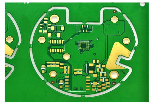
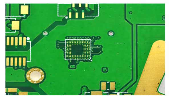

Microvias, Blind Vias, and Buried Vias in High-Density PCB Prototypes
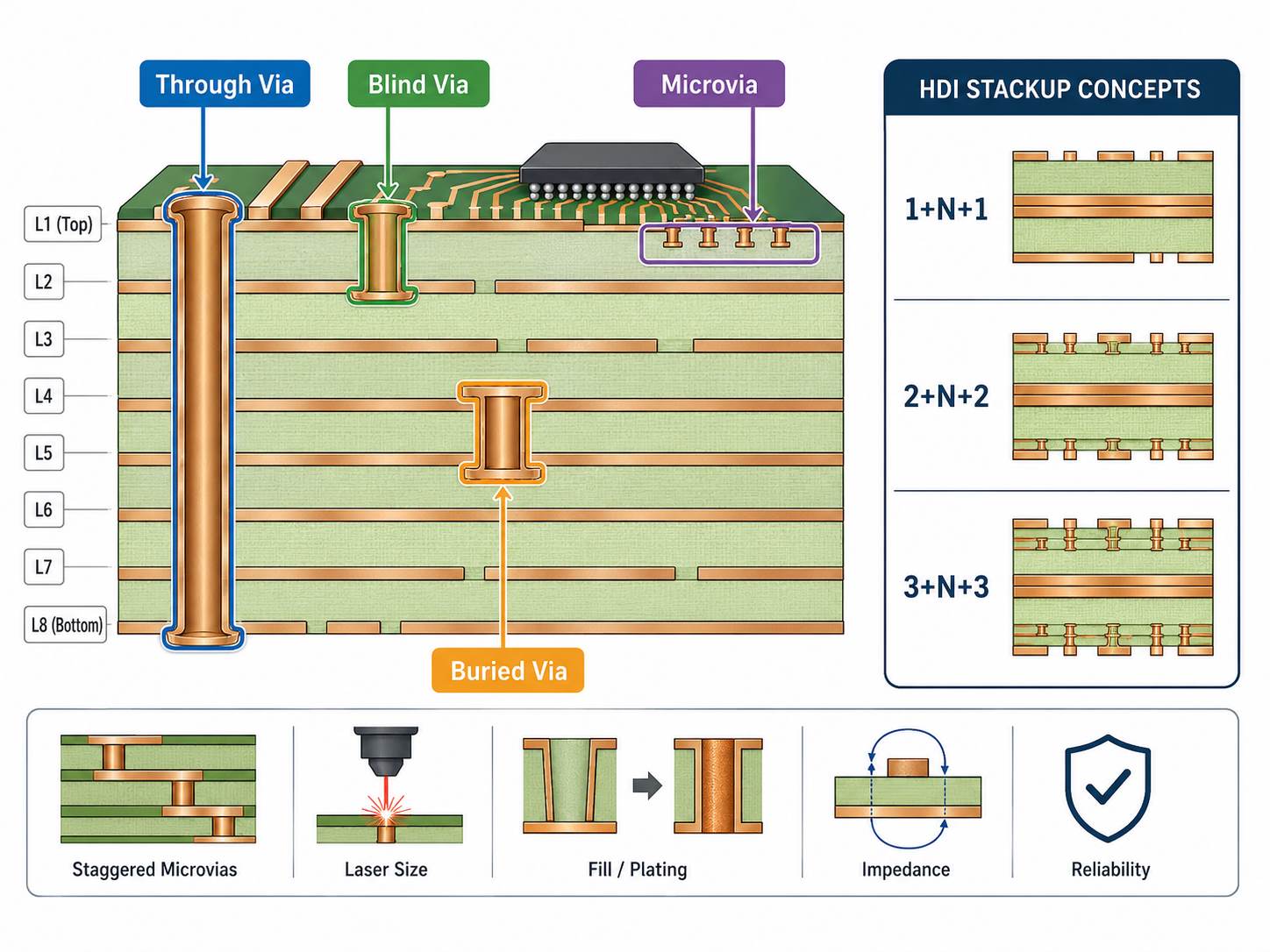
High-density interconnect PCB projects often depend on via structure. A standard through via connects from the top layer to the bottom layer. Blind vias connect an outer layer to one or more inner layers. Buried vias connect only internal layers. Microvias are usually laser-drilled small vias used for dense routing, especially around BGA areas.
For HDI boards, the structure is often described as 1+N+1, 2+N+2, or 3+N+3. The number outside the core structure shows build-up layers. More build-up layers usually mean more lamination steps, higher process complexity, and more production control points.
A manufacturer should check:
- Whether stacked or staggered microvias are used
- Whether the via structure matches lamination capability
- Whether laser via size and pad size are manufacturable
- Whether resin filling or via plating is needed
- Whether the via structure affects impedance, reliability, or yield
This is where high-density PCB prototypes require engineering review, not only price comparison.
Stackup and Material Review for High-Density PCB Prototypes
Stackup review is one of the most important steps in high-density PCB prototype manufacturing. The stackup affects impedance, drilling, lamination, warpage, copper balance, thickness tolerance, and assembly stability.
A practical stackup review should check:
- Total finished thickness
- Core and prepreg selection
- Copper thickness
- Signal, power, and ground layer arrangement
- Impedance reference layers
- Material availability
- Copper balance between layers
- Lamination risk
- Final surface finish
For HDI prototypes, stackup review is especially important when the board uses thin dielectrics, high-Tg material, heavy copper, buried vias, laser vias, or controlled impedance. If a material is not commonly stocked, it should be discussed before production because material lead time can directly affect delivery.
EBest Circuit has supported PCB and PCBA projects since 2006, and many engineering and production team members have worked with complex stackup, material, and process questions for more than 10 years. That experience matters most when a prototype file looks manufacturable at first glance but still contains hidden process risk.
Controlled Impedance and BGA Via-in-Pad Risks in HDI Prototypes
Controlled impedance is common in high-density PCB prototypes used for imaging products, communication modules, embedded systems, industrial controllers, and high-speed data boards. The manufacturer should not wait until the end of production to think about impedance. Trace width, dielectric thickness, copper thickness, reference layer, and tolerance must be reviewed before production.
BGA via-in-pad is another major risk. If a via is placed inside or near a BGA pad, solder can flow into the via during reflow. This may cause insufficient solder volume, weak joints, hidden opens, or X-Ray inspection difficulty.
Common manufacturing controls include:
- Resin-filled vias
- Plated-over vias
- Planarization
- Proper solder mask opening
- ENIG surface finish
- BGA pad and via review before fabrication
If the prototype will be assembled after PCB fabrication, these details should be reviewed as PCB plus PCBA requirements, not as two separate jobs.
Quick-Turn High-Density PCB Prototypes and Lead Time Factors
For high-density PCB prototypes, lead time depends on more than the order quantity. Even if the customer only needs 5 or 10 pcs, the board still goes through engineering review, stackup confirmation, drilling, plating, imaging, solder mask, surface finish, electrical testing, and final inspection.
For standard FR4 prototype boards under 1 square meter, EBest Circuit can usually support the following reference lead times:
| PCB Type | Normal Lead Time | Fastest Lead Time |
|---|---|---|
| 1-layer FR4 prototype | 7 days | 24 hours |
| 2-layer FR4 prototype | 8 days | 24 hours |
| 4-layer FR4 prototype | 10 days | 48 hours |
| 6-layer FR4 prototype | 10 days | 72 hours |
| 8-layer FR4 prototype | 12 days | 72 hours |
| 10-layer or above | To be confirmed | To be confirmed |
For high-density PCB prototypes, the final lead time should be confirmed after file review because the following requirements may add process time:
- HDI stackup or sequential lamination
- Blind vias, buried vias, or microvias
- Via-in-pad, resin filling, or copper paste filling
- Controlled impedance and test coupons
- Heavy copper or high-Tg material
- ENIG or other special surface finishes
- Tight line/space or small finished holes
- 100% electrical testing, inspection reports, or PCBA assembly
For projects that also need assembly, EBest Circuit can support PCB fabrication, component sourcing, SMT assembly, testing, and packing under one workflow. PCBA prototype lead time can be as fast as 2 days for urgent assembly projects, while normal PCBA service is usually about 1 week after PCB and components are ready.
The safest way to confirm lead time is to send the Gerber files, stackup drawing, BOM, assembly notes, impedance requirements, and delivery target before production. This helps the engineering team check whether the prototype can follow a fast-turn schedule or needs a more controlled manufacturing plan.
USA PCB Prototype Manufacturers vs Overseas HDI PCB Suppliers
USA PCB prototype manufacturers are useful when a project needs domestic production, local communication, or local compliance. Many USA suppliers also have strong experience in aerospace, medical, RF, and high-reliability PCB work.
Overseas HDI PCB suppliers can be useful when the buyer needs:
- Competitive prototype and small-batch cost
- Flexible engineering communication
- PCB fabrication plus component sourcing
- SMT assembly and testing
- Broader PCB options under one supplier
- Production scalability after prototype validation
For USA engineering teams, the decision does not have to be “USA supplier or overseas supplier” in a simple way. A practical sourcing strategy is to match the supplier to the project risk.
Choose domestic manufacturing when local control is mandatory. Choose a qualified overseas partner when the project needs HDI capability, PCBA support, cost control, and responsive engineering review.
High-Density PCB Prototype Case Study for a USA Project
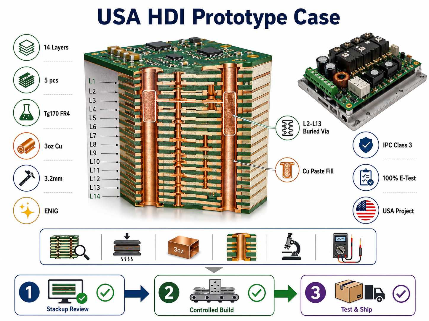
A USA customer needed a small-batch high-density PCB prototype for an industrial power control module. The order quantity was only a few pieces, but the board structure and reliability requirements were closer to a demanding production project than a simple prototype.
Project requirements
- Customer region: USA
- Application: Industrial power control module
- Quantity: 5 pcs prototype build
- PCB type: 14-layer high-density PCB
- Material: High-Tg FR4, Tg170
- Copper thickness: 3oz inner and outer layers
- Finished thickness: 3.2mm +/-10%
- Surface finish: ENIG 2u”
- Via structure: L2-L13 buried vias
- Via process: Copper paste filled vias
- Quality level: IPC Class 3 requirement
- Testing: 100% electrical test before shipment
- Production control: Production stackup and files confirmed with the customer before fabrication
Manufacturing challenges
- The 14-layer structure required stackup review before production.
- 3oz copper increased lamination and resin filling risk.
- Buried vias and copper paste filled vias had to be planned before final build.
- The prototype quantity was small, but the inspection requirement was strict.
- Board thickness, heavy copper, and buried via structure had to be controlled together.
EBest Circuit solution
- Reviewed the customer files and prepared a production-ready stackup.
- Confirmed production files and stackup with the customer before manufacturing.
- Planned buried via and copper paste filling requirements before lamination.
- Controlled heavy copper and board thickness to reduce warpage and lamination risk.
- Used ENIG surface finish for stable solderability and surface protection.
- Performed 100% electrical testing before shipment.
- Followed IPC Class 3 quality requirements for the build.
Result
The customer received a high-density prototype that matched the required layer structure, heavy copper design, buried via process, surface finish, and inspection standard. For this project, the value was not only producing five boards. The value was turning a complex prototype into a controlled manufacturing path before functional validation and possible next-stage production.
Why Work with EBest Circuit for High-Density PCB Prototype Projects?
EBest Circuit is suitable for high-density PCB prototype projects when the customer needs engineering support, not only bare PCB fabrication.
The company provides PCB fabrication, HDI PCB manufacturing, component sourcing, SMT assembly, testing, DFM review, BOM review, and production communication. This helps keep important details visible from file review to final delivery.
What this means for prototype projects
- Stackup, material, and copper thickness are reviewed before production.
- HDI via structures are checked before lamination.
- BGA via-in-pad risks are reviewed before SMT.
- Impedance requirements can be planned with coupons and reports.
- Production files can be confirmed before fabrication starts.
- PCB and PCBA requirements stay under one workflow when assembly is needed.
- Quality inspection, electrical testing, and shipment documents can be prepared according to project needs.
EBest Circuit has served engineers across more than 40 countries and supports quality systems including ISO9001, ISO13485, IATF16949, AS9100D, REACH, RoHS, and UL-related requirements. For high-density prototypes, that background helps when the project needs both fast response and controlled production discipline.
FAQs about High-Density PCB Prototypes and Manufacturers
1. What makes a PCB prototype “high-density”?
A high-density PCB prototype usually has tighter routing, smaller vias, finer line/space, BGA components, blind or buried vias, microvias, or controlled impedance requirements. HDI PCB is one common type of high-density PCB.
2. What is the difference between HDI PCB and standard multilayer PCB?
A standard multilayer PCB often uses through holes for interconnection. An HDI PCB may use laser microvias, blind vias, buried vias, sequential lamination, and finer routing to support compact and high-performance electronics.
3. Can high-density PCB prototypes be made quickly?
Yes, but the lead time depends on material, layer count, via structure, lamination steps, surface finish, impedance testing, and assembly requirements. A realistic lead time should be confirmed after file review.
4. Why is BGA via-in-pad risky in HDI prototypes?
If via-in-pad is not treated correctly, solder may flow into the via during reflow. This can cause weak BGA joints, insufficient solder, hidden opens, or difficult X-Ray inspection. Resin filling and plated-over vias are common controls.
5. What files should I send for a high-density PCB prototype quote?
Please send Gerber or ODB++ files, stackup drawing, drill files, impedance notes, BOM, placement file, assembly notes, surface finish requirements, panel requirements, and any inspection or report requirements.
If you are comparing manufacturers for a high-density PCB prototype, you do not have to make the sourcing decision from a price sheet alone. Send your Gerber files, stackup drawing, BOM, impedance notes, or assembly requirements to sales@bestpcbs.com. EBest Circuit’s engineering team can review the manufacturing path before production, so your prototype starts with clearer risks, clearer process control, and a supplier team that understands both PCB fabrication and PCBA delivery.
You may also like




Tags: best manufacturers high-density pcb prototypes usa, HDI PCB Prototype Manufacturer, High-Density PCB Prototypes