

Is a 5G circuit board project difficult due to RF loss, material mismatch, impedance issues, prototype failure, or assembly gaps? EBest provides design review, prototype support, PCB fabrication, assembly, and turnkey delivery to reduce production risk, improve manufacturability, and support stable high-frequency PCB performance.
What problems do OEM teams often face when sourcing 5G circuit board design, prototype, and assembly projects?
- Design risk: Stack-up, RF layout, impedance rules, antenna area, via structure, and ground reference are not reviewed before production.
- Material selection uncertainty: FR4, high-Tg FR4, Rogers, PTFE, hybrid stack-up, HDI PCB, or 5G flexible circuit boards are not matched to frequency, loss, heat, and cost targets.
- Prototype failure risk: The first 5G circuit board prototype may fail because line width, spacing, dielectric thickness, copper roughness, and impedance control were not checked early.
- Unclear prototype feedback: Test results, impedance data, soldering performance, and layout improvement points are not converted into clear changes before mass production.
- Assembly handoff gaps: PCB fabrication and 5G circuit board assembly are handled separately, causing BOM mismatch, SMT placement issues, RF connector problems, or delayed testing.
- Incomplete PCBA requirements: BOM, placement file, assembly drawing, polarity notes, shielding, functional test, and inspection standards are not fully confirmed before assembly.
EBest reduces these risks through early engineering review, prototype validation, and practical assembly support:
- Design review: We review stack-up, impedance, RF trace rules, via structure, material, copper thickness, surface finish, and manufacturability.
- Material matching: We match FR4, high-Tg FR4, Rogers, PTFE, hybrid stack-up, HDI PCB, or 5G flexible circuit boards based on frequency, heat, and structure.
- Prototype support: We support small-batch builds to verify material, impedance, solderability, assembly fit, and production feasibility.
- Prototype improvement: We review prototype feedback, impedance results, assembly issues, testing notes, and file updates before batch production.
- PCBA coordination: We combine PCB fabrication and assembly to reduce BOM errors, SMT handoff delays, and RF component issues.
- Assembly control: We provide BOM review, SMT, DIP, AOI, X-ray, RF connector assembly, shielding, functional testing, and custom inspection.
Welcome to contact us if you have any request for 5G circuit board manufacturing and assembly: sales@bestpcbs.com.
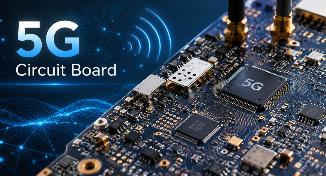
What Is a 5G Circuit Board?
A 5G circuit board supports RF signals, digital control, power paths, antenna modules, and high-speed data transmission. It requires tighter control of signal loss, impedance, heat, and interference than a standard PCB.
A 5G printed circuit board may use rigid PCB, HDI PCB, flexible PCB, rigid-flex PCB, high-frequency PCB, or hybrid stack-up.
The final structure depends on frequency band, antenna layout, signal path, assembly density, power level, and reliability target.
What Materials Are Used for 5G Circuit Boards?
Material choice affects RF loss, impedance stability, heat control, and PCB reliability. The right laminate should match frequency, stack-up, power level, and assembly method.
Material choice affects signal loss, impedance stability, thermal behavior, and PCB reliability.
High-Tg FR4 can support control circuits and lower-frequency areas.
Low-loss materials are better for RF paths, antenna sections, microwave circuits, and high-speed communication layers.
| Material | Typical Use | Key Value | Common Range |
|---|---|---|---|
| High-Tg FR4 | Control circuit | Cost control | Tg 150–180°C |
| Rogers | RF path | Low loss | Dk 2.2–3.5 |
| PTFE | Microwave area | Stable dielectric | Dk 2.1–2.9 |
| Hydrocarbon ceramic | Antenna/RF | Low Df | Df 0.001–0.004 |
| LCP | Flexible RF | Low moisture | Dk 2.9–3.2 |
| Hybrid stack-up | Mixed circuits | Balanced cost | 4–20 layers |
What Are the Main Types of 5G Circuit Boards?
Different 5G products require different PCB structures. The right type depends on RF performance, routing density, bending demand, product size, and assembly requirements.
Main 5G circuit board types include high-frequency PCB, HDI PCB, multilayer PCB, flexible PCB, and rigid-flex PCB.
Each type fits different product structures, RF requirements, assembly density, and space limits.
- High-frequency PCB: Used for RF transmission, antenna paths, filters, and microwave circuits.
- HDI PCB: Used for compact 5G modules with fine-pitch components and dense routing.
- Multilayer PCB: Used for boards that combine RF, digital, power, and control circuits.
- 5G flexible circuit boards: Used for antenna connections, compact wireless devices, and bendable structures.
- Rigid-flex PCB: Used for folding structures, space-saving layouts, and stable interconnects.
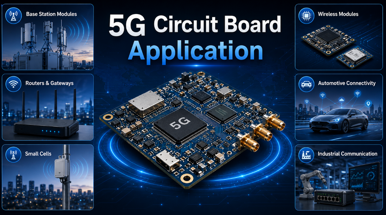
Where Are 5G Circuit Boards Commonly Used?
5G circuit boards are used in products that require stable wireless signal, compact layout, and reliable assembly. Common areas include telecom, wireless modules, automotive connectivity, and industrial communication.
- Base station modules: RF boards, antenna boards, power boards, and control boards.
- Routers and gateways: High-speed wireless communication products.
- Small cells: Compact indoor or urban 5G coverage devices.
- Wireless modules: IoT, tracking, monitoring, and communication modules.
- Automotive connectivity: V2X modules, telematics, and wireless control units.
- Industrial communication devices: Remote monitoring, wireless control, and smart equipment.
What Are the Technical Requirements for 5G Circuit Boards?
A reliable 5G circuit board depends on controlled impedance, low-loss material, stable stack-up, thermal control, fine routing, and suitable surface finish.
Core requirements include impedance control, low-loss material, stable stack-up, thermal control, fine routing, and reliable finish.
| Item | Recommended Control |
|---|---|
| Impedance tolerance | ±5% to ±10% |
| RF line width | Based on stack-up |
| Minimum line/space | 3/3 mil or tighter |
| Layer count | 4–20+ layers |
| Copper thickness | 0.5–3 oz |
| Surface finish | ENIG, ENEPIG, immersion silver |
| Via type | Through, blind, buried, back-drilled |
| Thermal range | Product class |
| Testing | E-test, AOI, impedance test |
How to Design a 5G Circuit Board for High-Frequency Performance?
Good 5G circuit board design starts with frequency, stack-up, material, impedance, grounding, routing, vias, and heat control. These items should be reviewed before prototype production.
Design must control frequency, stack-up, material, impedance, RF routing, grounding, vias, and thermal management.
- Confirm the working frequency first: This guides laminate choice, trace geometry, connector type, and antenna clearance.
- Define the stack-up early: Control dielectric thickness, copper weight, layer order, and reference planes.
- Choose the right PCB material: Use FR4 for control circuits and low-loss laminates for RF paths.
- Control impedance: Match trace width, spacing, dielectric height, copper thickness, and solder mask rules.
- Keep RF routing clean and short: Avoid unnecessary bends, stubs, vias, and sudden width changes.
- Protect the reference ground plane: Continuous ground improves return current and reduces noise.
- Manage via structure carefully: Use blind vias, buried vias, back-drilling, or via-in-pad only when required.
- Separate RF, digital, and power sections: Use spacing, shielding, and grounding to reduce interference.
- Plan heat dissipation early: Power amplifiers and RF modules require stable thermal paths.
- Check DFM before fabrication: Confirm line width, spacing, holes, annular ring, solder mask, and panelization.
How Does the 5G Circuit Board Manufacturing Process Work?
The manufacturing process turns design files into a functional high-frequency PCB. For 5G PCB production, material control, copper quality, via reliability, and impedance consistency are critical.
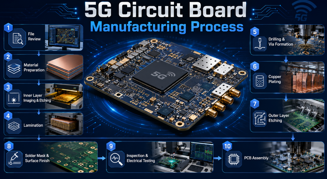
Step-by-step process for 5G PCB production:
1. File review: Check Gerber, drill files, stack-up, impedance notes, BOM, placement files, and test requirements.
2. Material preparation: Prepare FR4, high-Tg FR4, Rogers, PTFE, LCP, or hybrid laminates; check batch, thickness, and copper foil.
3. Inner layer imaging and etching: Form inner circuits; control line width, spacing, copper balance, and registration.
4. Lamination: Press inner layers, prepreg, and copper foil to form multilayer stack-up; control pressure and temperature.
5. Drilling and via formation: Mechanical or laser drilling, blind/buried vias, back-drilling; ensure hole quality.
6. Copper plating: Plate through holes and via walls; check plating thickness and uniformity.
7. Outer layer imaging and etching: Form outer circuit; control trace width and spacing for RF paths.
8. Solder mask and surface finish: Apply solder mask and finish, such as ENIG, ENEPIG, or immersion silver.
9. Inspection and electrical testing: Use AOI, E-test, impedance coupon test, visual check, and dimension inspection.
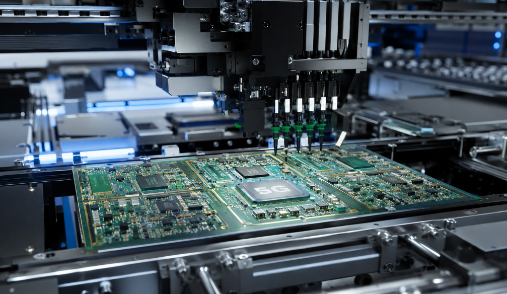
10. PCB assembly if required: SMT, DIP, solder paste printing, component placement, reflow, AOI, X-ray, cleaning, and functional testing.
What Should Be Confirmed Before 5G Circuit Board Assembly?
Before assembly starts, BOM, placement file, polarity, RF components, soldering plan, inspection method, and testing requirements should be confirmed to reduce SMT errors and rework.
Confirm BOM, placement, polarity, RF components, solder paste, inspection, and test plan.
- BOM: Part number, value, package, brand, tolerance, and alternatives.
- Placement file: X/Y location, rotation, side, and reference designator.
- RF components: Connectors, filters, amplifiers, shielding.
- Polarity notes: Diodes, LEDs, ICs, tantalum capacitors.
- PCB finish: ENIG, ENEPIG.
- Soldering plan: Paste type, stencil thickness, reflow profile.
- Inspection method: AOI, X-ray, visual, impedance, functional.
- Special requirements: Shielding, programming, labeling, cleaning, conformal coating, packaging, fixture testing.
Why Choose EBest as Your 5G Circuit Board Manufacturer?
A strong 5G circuit board manufacturer should support material selection, design review, PCB fabrication, assembly, testing, and delivery in one clear workflow. EBest helps reduce communication gaps and production risk.
EBest helps reduce 5G circuit board project risk by combining material selection, design review, prototype validation, PCB fabrication, assembly, and inspection in one workflow.
With over 20 years of experience, EBest supports high-frequency PCB, HDI PCB, flexible PCB, rigid-flex PCB, RF PCB, and impedance control PCB projects. This provides clearer technical review, smoother production handoff, stable quality control, and faster quotation response.
- Comprehensive PCB capabilities: FR4, multi-layer, metal-core, ceramic, semi-rigid flex, HDI, high-Tg, heavy copper, impedance control PCBs.
- Expedited service: Urgent boards can be completed and shipped within 24 hours.
- Strict quality certifications: IATF 16949, ISO 9001, ISO 13485, AS9100D, RoHS, REACH, UL.
- Customized solutions: Personalized support, DFM review, material selection, and design verification.
- Turnkey project support: End-to-end oversight from design review, prototype, fabrication, assembly, and functional testing.
Case Study: 5G Tower Circuit Board Project
This 5G tower circuit board project required stable RF performance, controlled impedance, thermal control, shielding, and reliable assembly. EBest managed the project from file review to prototype validation and batch production.
- Project Background: A telecom provider needed a high-frequency 5G tower PCB integrating RF, antenna, power, and digital circuits.
- Project Requirements: Stable RF, low insertion loss, controlled impedance, thermal management, SMT and through-hole assembly, shielding, functional testing.
- Challenges: Complex multilayer stack-up, impedance ±5% tolerance, dense component placement, coordination of fabrication and assembly.
- EBest Solutions: Full file review, low-loss laminate selection, prototype validation, integrated PCB fabrication and assembly, strict QC inspections.
- Results: Prototype met RF, thermal, and assembly requirements; mass production achieved high yield and repeatable quality; on-time delivery with minimal revisions.
FAQs About 5G Circuit Boards
Q1: What file package is needed for a quote?
A1: Gerber, drill files, stack-up, impedance notes, BOM, placement file, assembly drawing, and test instructions.
Q2: Which materials are suitable for high-frequency 5G PCBs?
A2: Rogers, PTFE, LCP, hybrid stack-ups, and high-Tg FR4.
Q3: What inspections does EBest provide?
A3: AOI, X-ray, E-test, impedance testing, visual inspection, and functional testing.
Q4: Can EBest handle both prototype and volume production?
A4: Yes. Small-batch prototypes, pilot runs, and mass production are supported.
Q5: How is impedance controlled?
A5: Through stack-up design, trace width, spacing, dielectric thickness, copper thickness, and test coupons.
Q6: What is the typical layer count?
A6: 4–20+ layers, depending on RF routing, shielding, and component density.
Q7: What affects 5G circuit board cost most?
A7: Material type, layer count, impedance, copper thickness, via structure, surface finish, assembly scope, and testing requirements.
Get a Fast Quote for Your 5G Circuit Board Project
A clear quote starts with complete project files. Send Gerber, BOM, stack-up, impedance notes, and test requirements to EBest for fast review and practical production feedback.
EBest Circuit provides customized, high-frequency 5G PCB solutions from design review to turnkey delivery. Ensure your project meets RF, thermal, and assembly requirements efficiently. Contact us now at sales@bestpcbs.com to get a fast, accurate quote and professional support from concept to delivery.
You may also like


Tags: 5G Circuit Board Assembly, 5G Circuit Board Design, 5G Circuit Board Manufacturer, 5g printed circuit board