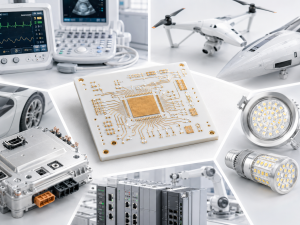
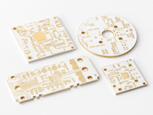
PCB manufacturing PCB manufacturing
Home > Blog

ceramic pcb manufacturing

Ceramic PCB for RF: Substrate Materials, Design Benefits, and Manufacturing Guide
Friday, July 10th, 2026

What Is a Ceramic PCB for RF?

A ceramic PCB for RF is a circuit board or substrate used in high-frequency circuits where dielectric stability, low signal loss, dimensional accuracy, and thermal reliability matter more than standard PCB cost.
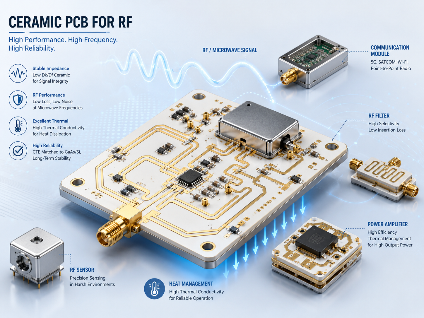
Ceramic PCB for RF modules, microwave filters, sensors, and power amplifiers

In RF and microwave applications, the substrate is part of the electrical design. It affects impedance, insertion loss, resonance behavior, signal phase, and long-term stability. This is why engineers often consider ceramic PCB substrate options such as alumina PCB for RF modules, microwave circuits, filters, sensors, power amplifiers, and hybrid circuits.

Why Ceramic PCB Substrate Matters in RF Circuits?

A ceramic PCB substrate matters in RF circuits because high-frequency signals are sensitive to material behavior. Small changes in dielectric constant, trace geometry, surface quality, or substrate thickness can shift impedance and affect performance.

For buyers, the key point is simple: RF ceramic PCB is not selected only for heat dissipation. The material must support stable signal behavior at the target frequency. A supplier must understand both ceramic PCB manufacturing and the RF requirements behind the drawing.

Key RF Properties: Dielectric Constant, Loss Tangent, and Dimensional Stability

For RF ceramic PCB projects, three material properties usually matter most: dielectric constant, loss tangent, and dimensional stability.
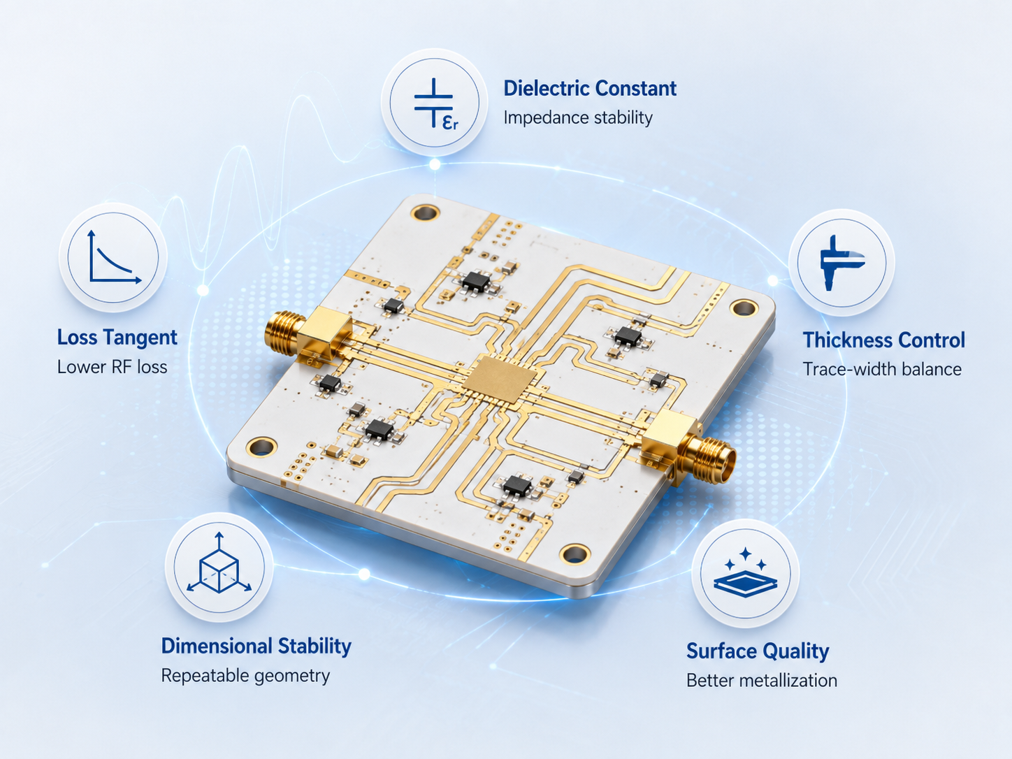
Ceramic PCB for RF modules, microwave filters, sensors, and power amplifiers
RF PropertyWhy It MattersBuyer Note
Dielectric constantAffects impedance, wavelength, trace width, and circuit sizeConfirm the value required by the RF design, not only the material name
Loss tangentAffects signal loss at high frequencyLower loss is more important as frequency increases
Substrate thicknessAffects impedance and manufacturable line widthKeep thickness controlled and clearly specified
Dimensional stabilityHelps maintain trace geometry and circuit repeatabilityImportant for filters, antennas, resonators, and microwave circuits
Surface qualityAffects metallization and high-frequency current behaviorReview finish and metallization process early

A good RF ceramic PCB quote should not start with “Can you make ceramic PCB?” It should start with frequency range, impedance target, material requirement, line width, tolerance, and metallization needs.

Common Materials: Alumina PCB, AlN, Rogers, and FR4

Material choice depends on frequency, loss target, thermal demand, cost, and manufacturing method. Alumina PCB is common in RF ceramic substrate applications, but it is not the only option.

MaterialRF StrengthLimitationBest Use
Alumina PCBStable ceramic substrate, good mechanical and thermal behavior, widely used in RF and hybrid circuitsHigher dielectric constant than many organic RF laminates; design must account for itRF modules, microwave circuits, sensors, hybrid circuits
Aluminum nitride PCBBetter thermal conductivity than aluminaHigher cost; not always needed for RF unless heat is also a major issueRF power modules, high-power microwave circuits, compact thermal designs
Rogers / PTFE-based RF laminateCommon for RF PCB design, lower-loss options availableMaterial and processing cost can be higher than FR4; thermal/mechanical behavior differs from ceramicAntennas, RF boards, microwave circuits, communication devices
FR4Low cost and easy to manufactureLoss and dielectric variation become problematic at higher frequenciesLow-frequency or cost-sensitive circuits where RF loss is acceptable

For many RF ceramic PCB projects, alumina PCB is selected when the design needs ceramic stability, precision metallization, and reliable high-frequency behavior in a compact substrate.

Ceramic PCB for RF vs Standard RF PCB Materials

The decision between ceramic PCB and standard RF laminate depends on circuit function, frequency, power level, size, and reliability environment.

OptionAdvantageLimitationBetter Fit
Ceramic PCB for RFStable substrate, good thermal behavior, suitable for hybrid and precision circuitsHigher cost and stricter manufacturing limitsRF modules, microwave packages, high-stability circuits
Rogers RF PCBMature RF laminate option with known dielectric choicesNot ceramic; thermal and mechanical behavior differAntennas, RF communication boards, microwave PCB layouts
FR4 RF designLow cost and fast productionHigher loss and less predictable dielectric behavior at high frequencyLow-frequency RF, simple prototypes, cost-sensitive products
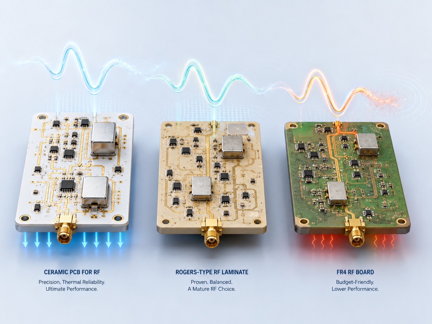
RF performance comparison between ceramic PCB, Rogers laminate, and FR4 board

The practical takeaway: use FR4 only when RF loss and dielectric variation are acceptable. Use Rogers-type RF laminates for many standard RF boards. Use ceramic PCB when the design needs ceramic stability, compact structure, precision, or stronger thermal reliability.

Ceramic PCB Manufacturing Considerations for RF Applications

Ceramic PCB manufacturing for RF applications must control the details that affect signal performance. A small trace width error may be more serious in RF than in a normal power or control PCB.

Important manufacturing points include:

  • Substrate material and thickness control
  • Fine line and spacing capability
  • Metallization method, such as thick film, thin film, DBC, or other suitable process
  • Copper or conductor thickness
  • Surface roughness and finish
  • Dimensional tolerance
  • Via and hole quality if required
  • Flatness and warpage
  • Pattern registration
  • Cleanliness and handling

For RF ceramic PCB manufacturing, the supplier should review whether the requested geometry is manufacturable before production. If the layout uses very fine traces, tight impedance targets, or microwave structures, early engineering communication reduces prototype failure risk.

When Should You Choose Alumina PCB for RF?

Choose alumina PCB for RF when the circuit needs a stable ceramic substrate, good dimensional control, and reliable behavior in a compact or harsh environment.

Alumina PCB is often suitable for:

  • RF hybrid circuits
  • Microwave modules
  • Sensor circuits
  • Thin film or thick film RF substrates
  • Filters and matching networks
  • High-temperature or high-reliability electronics
  • Compact modules where ceramic stability is useful

Alumina may be unnecessary if the circuit can meet RF performance with a standard RF laminate at lower cost. It may also be the wrong choice if the design requires a different dielectric constant, lower loss material, or stronger thermal conductivity than alumina can provide.

Common Design and Purchasing Mistakes

The most common mistake is treating RF ceramic PCB like a normal ceramic circuit board. RF performance depends on both material and geometry.
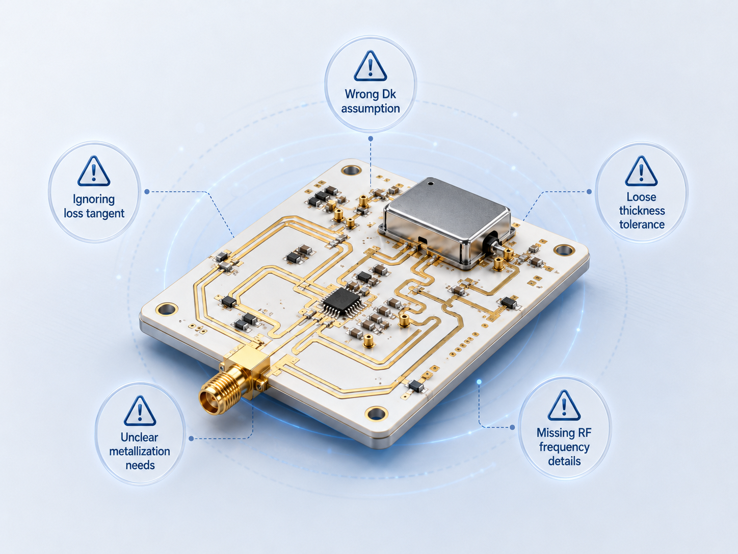
Common RF ceramic PCB mistakes including incorrect dielectric constant, loose tolerance, and missing frequency details
MistakeWhy It Causes ProblemsBetter Approach
Only asking for “ceramic PCB for RF”Supplier cannot confirm material, frequency, or processProvide frequency range, substrate material, and circuit function
Ignoring dielectric constantImpedance and trace width may shiftSpecify target dielectric constant or approved material
Ignoring loss tangentHigh-frequency loss may become unacceptableDefine frequency and acceptable RF performance
Using vague tolerancesRF traces may not match design intentSpecify line width, spacing, substrate thickness, and dimensional tolerance
Choosing alumina automaticallyAlumina may not fit every RF designCompare alumina, AlN, Rogers, and FR4 based on real requirements
Sending only GerbersSupplier cannot judge RF function or riskInclude stackup, material notes, impedance targets, and application context

A good ceramic PCB manufacturer should ask technical questions before quotation if the RF requirements are unclear.

How to Choose a Ceramic PCB Manufacturer for RF Projects?

A ceramic PCB manufacturer for RF projects should be evaluated by engineering communication, material control, metallization capability, and tolerance control, not only by price.

Useful supplier checks include:

  • Experience with RF or microwave ceramic substrate projects
  • Ability to manufacture alumina PCB and other ceramic PCB substrate types
  • Clear process options for thin film, thick film, or metallized ceramic circuits
  • Fine line and spacing capability
  • Substrate thickness and dimensional tolerance control
  • Inspection process for metallization, surface finish, and pattern accuracy
  • Willingness to review drawings before quoting
  • Ability to support prototypes before mass production
  • Clear communication about manufacturing limits and alternatives

For EBest Circuit (Best Technology), RF ceramic PCB review should focus on whether the drawing, material, tolerance, and production method match the actual frequency and application requirement.

What to Provide When Requesting an RF Ceramic PCB Quote

A complete RFQ helps the supplier evaluate manufacturability, cost, and performance risk before production.

Provide these details when requesting a ceramic PCB quote:

  • Application type, such as RF module, microwave circuit, sensor, or power amplifier
  • Frequency range
  • Ceramic material preference, such as alumina PCB or AlN
  • Required dielectric constant if specified
  • Loss requirement if specified
  • Substrate dimensions and thickness
  • Line width and spacing
  • Metallization method or conductor requirement
  • Copper or metal thickness
  • Surface finish
  • Hole, via, or edge requirements
  • Dimensional tolerance
  • Quantity for prototype and mass production
  • Test or inspection requirements
  • Gerber files, drawings, and stackup notes

If the project is still in early design, provide the target frequency, operating environment, and performance concern. This allows the ceramic PCB manufacturer to suggest practical material and process options before the design is locked.

FAQ

Is ceramic PCB good for RF?

Yes. Ceramic PCB can be good for RF when the circuit needs dielectric stability, dimensional accuracy, thermal reliability, and compact substrate design. It is especially useful for RF modules, microwave circuits, hybrid circuits, sensors, and high-reliability electronics.

Why is alumina PCB used in RF circuits?

Alumina PCB is used in RF circuits because it provides a stable ceramic substrate, good mechanical strength, useful thermal behavior, and compatibility with thin film or thick film metallization. It is common in RF and microwave hybrid circuits.

Is ceramic PCB better than Rogers PCB for RF?

Not always. Rogers-type RF laminates are widely used for RF PCB designs, antennas, and microwave boards. Ceramic PCB is better when the design needs ceramic stability, compact substrate behavior, precision metallization, or stronger thermal/mechanical reliability.

Can FR4 be used for RF circuits?

FR4 can be used for lower-frequency or cost-sensitive RF circuits, but it becomes less predictable as frequency increases. Loss, dielectric variation, and tolerance control can limit performance in higher-frequency RF designs.

What affects RF performance in ceramic PCB manufacturing?

RF performance can be affected by dielectric constant, loss tangent, substrate thickness, line width, spacing, metallization quality, surface roughness, dimensional tolerance, and pattern registration.

What is the difference between alumina PCB and AlN PCB for RF?

Alumina PCB is commonly used for RF ceramic substrates and is usually more cost-effective. AlN PCB offers higher thermal conductivity, so it is useful when the RF circuit also has significant heat dissipation requirements.

What should I ask a ceramic PCB manufacturer before ordering?

Ask about material options, RF project experience, fine line capability, metallization process, substrate thickness tolerance, dimensional tolerance, inspection method, prototype support, and whether they can review RF-related drawing requirements before production.

Do I need impedance control for ceramic PCB for RF?

Many RF ceramic PCB designs need impedance awareness, even if the supplier does not provide full RF simulation. At minimum, the buyer should provide frequency range, trace geometry, substrate thickness, dielectric requirement, and critical RF areas.

Conclusion

A ceramic PCB for RF is not just a ceramic version of a normal PCB. The substrate affects impedance, signal loss, circuit size, stability, and long-term performance. Alumina PCB is often a practical RF ceramic substrate, while AlN, Rogers materials, and FR4 each fit different design conditions.

If you are evaluating ceramic PCB substrate options, alumina PCB, ceramic PCB manufacturing, or RF PCB prototype support, EBest Circuit (Best Technology) can help review your drawings, material requirements, tolerance needs, and quotation details. Contact us at sales@bestpcbs.com.
You may also like

Ceramic PCB Manufacturer: Custom High-Temperature Circuit Boards for Reliable Electronics
Tuesday, June 23rd, 2026

Ceramic PCB manufacturer builds circuit boards on ceramic substrates instead of standard FR4 laminate. These boards are used when a project needs better heat dissipation, stronger insulation, higher temperature resistance, or stable performance in harsh operating environments. For engineers and buyers, choosing the right ceramic PCB manufacturer is not only about price. It is about material selection, process capability, quality control, delivery stability, and long-term production support.

Ceramic PCB Manufacturer: Custom High-Temperature Circuit Boards for Reliable Electronics

Ceramic PCBs are widely used in power electronics, aerospace systems, automotive modules, medical devices, LED lighting, RF equipment, industrial sensors, and high-reliability electronic assemblies. A qualified manufacturer should understand alumina, aluminum nitride, DPC, DBC, thick film, thin film, LTCC, HTCC, surface finishing, electrical testing, and assembly compatibility.

What Is a Ceramic PCB Manufacturer?

Ceramic PCB manufacturer is a company that designs, fabricates, tests, and supplies printed circuit boards based on ceramic substrates. Unlike standard PCB factories that mainly process FR4, a ceramic PCB manufacturer works with inorganic materials such as alumina, aluminum nitride, silicon nitride, or other advanced ceramics.

The main role is to convert ceramic substrates into reliable circuit carriers. This includes substrate selection, metallization, copper bonding, pattern imaging, etching, surface treatment, inspection, and final testing.

For high-power or high-temperature electronics, the manufacturer must control thermal conductivity, dielectric strength, copper adhesion, surface flatness, and dimensional tolerance. A small process error can affect soldering, heat transfer, or long-term reliability.

Why Are Ceramic PCBs Important in Modern Electronics?

Ceramic PCBs are important because many modern electronic products generate more heat in a smaller space. Standard FR4 boards are useful for many applications, but they have thermal limits. When heat cannot move away from components efficiently, devices may suffer from performance drift, solder fatigue, insulation breakdown, or early failure.

Ceramic materials offer high thermal conductivity, good electrical insulation, low thermal expansion, and strong resistance to moisture, chemicals, and high temperatures. This makes them suitable for power modules, LED packages, automotive electronics, aerospace controls, laser systems, RF circuits, and medical devices.

For buyers, ceramic PCBs are often selected when product reliability is more valuable than the lowest board cost.

How Does a Ceramic PCB Work?

A ceramic PCB works as both an electrical circuit carrier and a thermal management platform. Conductive layers carry current and signals, while the ceramic substrate transfers heat away from hot components.

In a typical design, copper or metalized conductors are bonded to a ceramic base. Components are mounted on the circuit layer. When the device operates, heat moves from the component into the copper and then into the ceramic substrate. From there, heat can spread to a heatsink, housing, or cooling structure.

This structure reduces hot spots and helps maintain stable electrical performance. It is especially useful for power devices, high-current circuits, RF modules, and compact assemblies where temperature control is critical.

What Types of Ceramic PCBs Can Manufacturers Produce?

Different ceramic PCB types are selected according to circuit density, copper thickness, temperature range, and application requirements.

Ceramic PCB TypeMain FeatureTypical Use
Alumina PCBCost-effective, stable, widely availableLED, sensors, industrial electronics
Aluminum Nitride PCBHigh thermal conductivityPower modules, aerospace, laser systems
DPC Ceramic PCBFine circuit pattern and plated copperHigh-density ceramic circuits
DBC Ceramic PCBThick copper bondingPower electronics, IGBT modules
Thick Film Ceramic PCBPrinted conductor paste, mature processSensors, heaters, hybrid circuits
Thin Film Ceramic PCBHigh precision and fine linesRF, microwave, precision electronics
LTCC PCBMultilayer ceramic with co-fired metalRF modules, compact electronic packages
HTCC PCBHigh-temperature co-fired ceramicHarsh environment electronics
AMB Ceramic SubstrateStrong copper-ceramic bondingEV power modules, industrial drives

A professional ceramic PCB manufacturer should not recommend one process for every project. The right choice depends on thermal load, circuit density, copper thickness, mechanical stress, working temperature, and target cost.

What Materials Are Used in Ceramic PCB Manufacturing?

The most common ceramic PCB materials are alumina and aluminum nitride.

Alumina, also called Al₂O₃, is widely used because it offers stable insulation, good mechanical strength, mature supply, and reasonable cost. It is suitable for many industrial, LED, sensor, and electronic control applications.

Aluminum nitride, also called AlN, is chosen when heat dissipation is the main concern. It has much higher thermal conductivity than alumina, making it suitable for power modules, laser diodes, high-power LEDs, RF amplifiers, aerospace electronics, and compact high-heat devices.

Other materials may include silicon nitride, zirconia-toughened alumina, beryllium oxide alternatives, LTCC ceramic tape, HTCC ceramic systems, tungsten, molybdenum, silver paste, silver-palladium paste, copper, nickel, gold, ENIG, ENEPIG, and other surface finish materials.

What Is the Ceramic PCB Manufacturing Process?

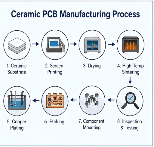
The ceramic PCB manufacturing process depends on the selected technology. However, a typical process may include material preparation, ceramic substrate cleaning, drilling or laser processing, metallization, copper deposition or bonding, imaging, etching, surface finish, testing, and packaging.

For DPC ceramic PCB fabrication, copper is usually deposited onto the ceramic surface through metallization and electroplating. This process supports fine lines, small spacing, and high precision.

For DBC ceramic PCB manufacturing, copper is directly bonded to ceramic under high temperature. It is suitable for thick copper and high-current power applications.

For thick film ceramic PCB production, conductive paste is printed onto the ceramic substrate and fired at high temperature. This process is common for sensors, heaters, and hybrid circuits.

Ceramic PCB Manufacturer: Custom High-Temperature Circuit Boards for Reliable Electronics

For LTCC and HTCC, ceramic layers and metal conductors are co-fired to form multilayer structures. These processes are used when compact multilayer ceramic integration is required.

What Are the Key Features of Ceramic PCBs?

Ceramic PCBs are valued for their thermal, electrical, and mechanical stability. Their most important features include high thermal conductivity, strong dielectric insulation, low thermal expansion, high temperature resistance, good chemical stability, and long service life in demanding environments.

They also support direct heat transfer from components to the substrate. This can reduce the need for complex thermal interface layers in some applications.

Another important feature is dimensional stability. Ceramic substrates do not expand and contract like many organic materials. This helps protect solder joints and components under repeated heating and cooling.

For precision electronics, ceramic PCBs can also support stable RF performance, low signal loss, and strong environmental resistance.

What Are the Advantages of Ceramic PCBs?

Ceramic PCBs offer several clear advantages for demanding electronic products.

They help remove heat more efficiently than standard FR4 boards. They maintain insulation under high voltage and high temperature. They resist moisture, corrosion, and harsh industrial environments. They also provide strong mechanical stability for compact assemblies.

For power electronics, ceramic PCBs can improve thermal paths and support higher current density. For aerospace and medical electronics, they help support reliability under strict operating requirements. For LED and laser applications, they help control junction temperature and extend product life.

The main advantage is not only performance. It is long-term stability in applications where failure is expensive.

What Are the Limitations of Ceramic PCBs?

Ceramic PCBs are not the best choice for every project. They usually cost more than FR4 boards. The material is harder and more brittle, so mechanical design must be handled carefully. Large panel sizes, complex shapes, or aggressive mechanical stress may increase production risk.

Some ceramic processes also require longer lead times, especially for multilayer LTCC, HTCC, DBC, or custom thick copper structures. Design changes after tooling or process setup may also increase cost.

For simple low-power circuits, FR4 may still be more economical. Ceramic PCBs should be selected when thermal, electrical, or environmental requirements justify the added cost.

How Do Alumina and Aluminum Nitride Ceramic PCBs Compare?

Alumina and aluminum nitride are the two most common materials buyers compare.

ItemAlumina PCBAluminum Nitride PCB
Main StrengthCost-effective and stableExcellent heat dissipation
Thermal PerformanceModerate to goodHigh
CostLowerHigher
Mechanical StrengthGoodGood, but process control is critical
Typical ApplicationsLED, sensors, controls, industrial boardsPower modules, aerospace, laser, RF, high-power LED
Best ForBalanced cost and reliabilityHigh thermal conductivity projects

If the product has moderate heat and needs a stable ceramic base, alumina is often suitable. If the product has high heat density or strict thermal control requirements, aluminum nitride is usually the better choice.

Ceramic PCB Manufacturer: Custom High-Temperature Circuit Boards for Reliable Electronics

How to Choose the Right Ceramic PCB Technology?

The right ceramic PCB technology should be selected according to the electrical, thermal, mechanical, and cost requirements of the project.

Choose DPC when the design needs fine circuits, plated vias, better pattern accuracy, or compact layouts. Choose DBC when the project needs thick copper, high current capacity, and strong thermal transfer. Choose thick film when the circuit is suitable for printed paste conductors and mature hybrid circuit production. Choose thin film when very fine lines, RF behavior, or precision circuits are required.

LTCC is suitable for compact multilayer ceramic modules, especially RF and high-frequency products. HTCC is suitable for very high-temperature and harsh environment systems. AMB is often used for power modules that require strong bonding strength and thermal cycling reliability.

Where Are Ceramic PCBs Commonly Used?

Ceramic PCBs are used in industries where heat, reliability, insulation, and long service life matter.

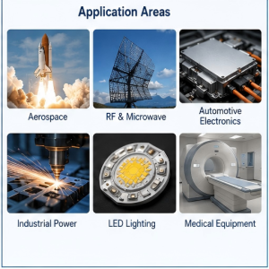
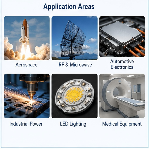
Common applications include automotive power modules, EV charging systems, aerospace control boards, radar and RF modules, medical imaging systems, surgical devices, laser equipment, high-power LED lighting, industrial sensors, IGBT modules, semiconductor packaging, photovoltaic inverters, and telecom equipment.

Ceramic PCB Manufacturer: Custom High-Temperature Circuit Boards for Reliable Electronics

In aerospace applications, AlN ceramic PCBs are often selected for thermal performance and stability. In automotive electronics, DBC or AMB ceramic substrates may be used in power modules. In medical and industrial devices, alumina ceramic PCBs are often selected for insulation, cleanliness, and stable performance.

Practical Case: Ceramic PCB for High-Power LED Lighting

A high-power LED project often fails when heat remains trapped near the LED chip. The result may include brightness decay, color shift, solder fatigue, or shortened service life.

In this situation, a ceramic PCB can create a shorter heat path from the LED package to the heatsink. Alumina may be enough for medium-power lighting. Aluminum nitride is better when the LED module has high power density or limited cooling space.

For manufacturing, the key points include copper thickness, solder mask compatibility, surface finish, flatness, thermal interface design, and assembly temperature control. A ceramic PCB manufacturer should review both the board design and the final heat dissipation structure.

Practical Case: AlN Ceramic PCB for Aerospace Electronics

Aerospace electronics often require stable operation under vibration, temperature cycling, and restricted space. For high-power control modules or RF systems, aluminum nitride ceramic PCBs can help move heat away from sensitive components while maintaining electrical insulation.

In this type of project, the manufacturer must control substrate quality, copper adhesion, circuit tolerance, surface cleanliness, and reliability testing. The design should also consider thermal expansion matching, solder joint stress, and mounting pressure.

The right aerospace AlN ceramic PCB board manufacturer should provide engineering review before production, not only quote the Gerber files.

What Should Engineers Consider During Ceramic PCB Design?

Ceramic PCB design should begin with thermal and mechanical planning. Engineers should define the heat source, heat path, copper thickness, component placement, mounting structure, and cooling method before finalizing the layout.

Trace width, spacing, via design, substrate thickness, copper balance, edge clearance, and surface finish should match the chosen process. Sharp corners, large unsupported areas, and uneven copper distribution may increase stress risk.

For DBC and AMB boards, copper thickness and thermal cycling must be reviewed carefully. For DPC and thin film boards, fine-line capability and plating uniformity are important. For LTCC and HTCC, shrinkage control and layer alignment must be considered early.

What Manufacturing Issues Should Be Controlled?

Ceramic PCB manufacturing requires strict process control. Important risks include poor copper adhesion, ceramic cracking, uneven plating, over-etching, line width variation, surface contamination, warpage, incomplete vias, and weak solderability.

A reliable ceramic PCB manufacturer should control each stage with inspection points. This may include incoming ceramic inspection, surface cleaning control, metallization inspection, copper thickness measurement, line width and spacing inspection, adhesion testing, electrical testing, visual inspection, AOI, X-ray inspection, and final packaging review.

For batch production, process stability matters more than a single good sample. Buyers should ask how the manufacturer controls repeatability from prototype to mass production.

What Affects Ceramic PCB Cost?

Ceramic PCB cost is affected by material type, substrate thickness, copper thickness, process method, circuit precision, panel utilization, surface finish, testing requirements, order quantity, and lead time.

Aluminum nitride usually costs more than alumina. DBC and AMB may cost more when thick copper and high bonding strength are required. LTCC and HTCC can be expensive because they involve multilayer ceramic processing and firing control.

Fine lines, small holes, tight tolerances, special surface finishes, and reliability tests also increase cost. For cost-effective ceramic PCB manufacturing, the best strategy is not to choose the cheapest material. It is to match the material and process to the real working condition.

How Is Ceramic PCB Quality Tested?

Ceramic PCB quality testing usually includes dimensional inspection, visual inspection, copper thickness measurement, line width and spacing check, open and short electrical test, surface finish inspection, solderability test, adhesion test, thermal shock test, and high-voltage insulation test when required.

For power electronics, thermal cycling and bonding strength are especially important. For RF and high-frequency applications, impedance, dielectric performance, and surface roughness may need review. For medical or aerospace projects, additional traceability and process documentation may be required.

A strong manufacturer should provide test records, inspection reports, and process traceability for critical projects.

What Standards and Certifications Matter?

Ceramic PCB projects may involve IPC, UL, RoHS, REACH, ISO 9001, ISO 13485, IATF 16949, or industry-specific customer standards. The exact requirement depends on the product market.

IPC standards are commonly used for PCB workmanship and acceptance expectations. UL may matter when the final product needs safety recognition. RoHS and REACH are important for restricted substance compliance. ISO 13485 is relevant for medical supply chains. IATF 16949 is important for automotive electronics projects.

For global buyers, certification is not only a document. It shows whether the supplier has a controlled quality system.

Common Ceramic PCB Failure Modes and Root Causes

Ceramic PCB failure usually comes from design mismatch, process instability, or assembly stress.

Common failure modes include ceramic cracking, copper delamination, solder joint fatigue, insulation breakdown, hot spots, poor solderability, via failure, and surface contamination. Cracking may come from mechanical pressure, poor mounting design, or thermal shock. Copper delamination may come from weak metallization, poor bonding, or improper thermal cycling. Hot spots may come from insufficient copper area, wrong substrate choice, or poor heatsink contact.

A practical failure analysis should review the full chain: material, design, manufacturing, assembly, mounting, and operating environment.

How to Choose a Reliable Ceramic PCB Manufacturer?

A reliable ceramic PCB manufacturer should have real ceramic process capability, not only standard PCB production experience. Buyers should check material options, DPC capability, DBC capability, thick film or thin film support, multilayer ceramic experience, surface finish options, inspection equipment, and batch production records.

The manufacturer should also review your design before production. Good questions from a supplier are a positive sign. They may ask about working temperature, power density, voltage, current, thermal path, soldering method, final assembly, and reliability requirements.

For global sourcing, choose a China source factory that can provide custom manufacturing, prototype support, low-volume production, batch production, engineering communication, and stable export documentation without claiming false overseas facilities.

What Should Buyers Check Before Placing an Order?

Before placing an order, buyers should prepare complete Gerber files, material requirements, substrate thickness, copper thickness, surface finish, tolerance requirements, quantity, working temperature, voltage, current, assembly method, and testing requirements.

It is also helpful to share the application background. A board used in LED lighting, EV power modules, aerospace electronics, or medical equipment may require different process controls.

Buyers should confirm lead time, minimum order quantity, sample approval process, inspection standards, packaging method, export documents, and after-sales technical support. For repeat orders, they should also confirm how the supplier controls material batches and process consistency.

Frequently Asked Questions About Ceramic PCB Manufacturers

What does a ceramic PCB manufacturer do?
A ceramic PCB manufacturer produces circuit boards based on ceramic substrates such as alumina or aluminum nitride. The work includes material selection, circuit formation, metallization, copper bonding, surface finish, inspection, testing, and sometimes PCB assembly support.

Is ceramic PCB better than FR4 PCB?
Ceramic PCB is better when the project needs high thermal conductivity, high temperature resistance, strong insulation, or long-term stability in harsh environments. FR4 is still suitable for many low-power or cost-sensitive circuits.

Which ceramic PCB material is most common?
Alumina is the most common ceramic PCB material because it offers stable performance and reasonable cost. Aluminum nitride is used when the design needs much better heat dissipation.

What is the difference between DPC and DBC ceramic PCB?
DPC is often used for fine circuits and plated copper structures. DBC is better for thick copper, high-current, and power module applications. The right choice depends on current, heat, circuit density, and reliability needs.

Can ceramic PCBs be multilayer?
Yes. Multilayer ceramic PCBs can be produced by LTCC, HTCC, or other advanced ceramic processes. They are used when compact structure, high reliability, or RF integration is required.

Are ceramic PCBs suitable for aerospace electronics?
Yes. Ceramic PCBs are suitable for aerospace applications when the design needs high heat resistance, stable insulation, low thermal expansion, and strong reliability under harsh operating conditions.

Why is aluminum nitride used in high-power ceramic PCBs?
Aluminum nitride is selected because it offers high thermal conductivity while maintaining electrical insulation. It helps move heat away from power components, lasers, RF modules, and compact high-power devices.

What makes ceramic PCB manufacturing expensive?
Cost comes from ceramic material price, copper bonding method, circuit precision, substrate thickness, copper thickness, surface finish, testing requirements, yield control, and order quantity. Advanced processes such as LTCC, HTCC, DBC, and AMB often cost more.

Can ceramic PCBs be used for PCB assembly?
Yes. Ceramic PCBs can support SMT assembly, wire bonding, die attach, soldering, and other assembly methods. The manufacturer should confirm surface finish, flatness, soldering profile, and component compatibility before production.

What files are needed for a ceramic PCB quotation?
A manufacturer usually needs Gerber files, drill files, material requirement, substrate thickness, copper thickness, surface finish, quantity, tolerance, testing requirements, and application information. For assembly, BOM and pick-and-place files are also needed.

How do I reduce ceramic PCB cost without reducing quality?
Use the right material instead of the most expensive one. Avoid unnecessary tight tolerances, oversized substrates, excessive copper thickness, and complex surface finishes unless the application requires them. Early engineering review can also reduce rework.

What is the lead time for ceramic PCB production?
Lead time depends on process type, material availability, complexity, quantity, and testing requirements. Simple alumina or AlN prototypes are usually faster than multilayer LTCC, HTCC, DBC, or AMB production.

How can I judge whether a ceramic PCB supplier is reliable?
Check whether the supplier understands ceramic materials, process limits, quality testing, thermal management, and application risks. A reliable supplier should provide engineering feedback, inspection support, and stable prototype-to-batch production service.

Are Chinese ceramic PCB manufacturers suitable for global buyers?
Yes, many global buyers choose Chinese ceramic PCB manufacturers for custom production, flexible engineering support, prototype service, low-volume orders, and batch manufacturing. Buyers should verify real factory capability, certifications, quality control, and export experience.

Conclusion:

Ceramic PCB manufacturer should do more than produce a circuit board. The right supplier should help engineers select the correct substrate, match the right manufacturing process, control thermal and electrical risks, and support stable production from prototype to mass order.

If your project requires ceramic PCB prototype development, low-volume production, mass manufacturing, or a custom thermal management solution, our engineering team can help review your design, recommend suitable materials, and provide a practical quotation. Please contact us with your Gerber files, BOM, drawings, or application requirements, and we will support you with OEM manufacturing, ODM production, sample development, batch production, and custom engineering solutions. Email: sales@bestpcbs.com

You may also like

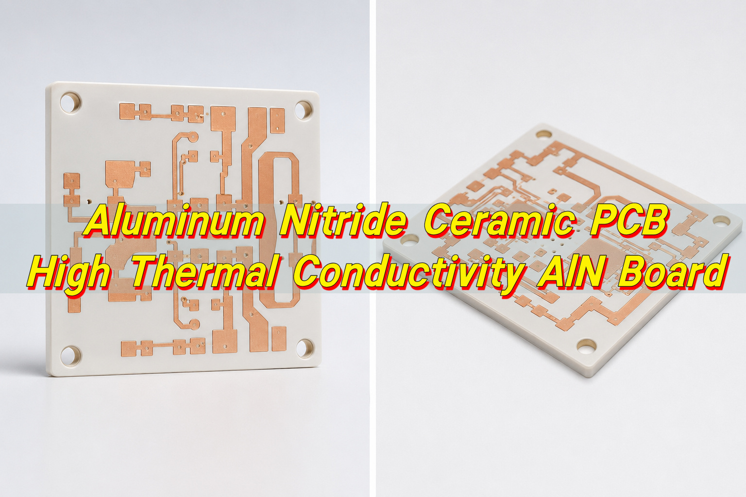
Aluminum Nitride Ceramic PCB | High Thermal Conductivity AlN Board
Tuesday, May 19th, 2026

What Is an Aluminum Nitride AlN Ceramic PCB Board?

An Aluminum Nitride ceramic PCB board is a high-performance circuit platform built on a ceramic base material rather than traditional fiberglass (FR4) or metal core substrates. Unlike standard boards, this structure uses aluminum nitride ceramic as the foundation, offering exceptional thermal conductivity combined with reliable electrical insulation.

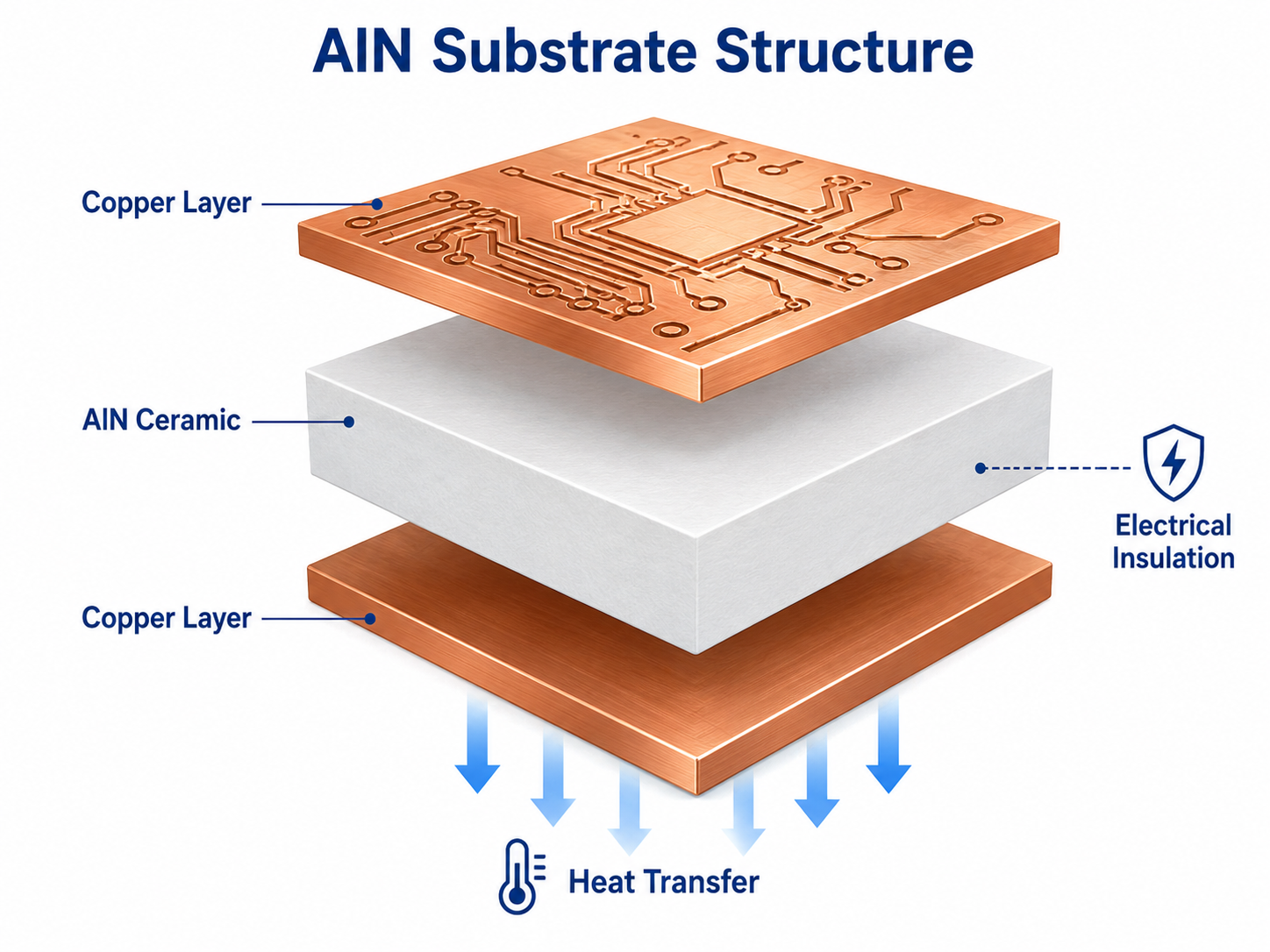
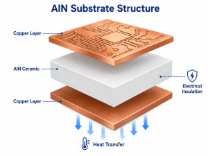
At its core, an AlN ceramic PCB integrates conductive copper circuitry onto a dense ceramic substrate. The ceramic layer acts as both a mechanical support and a thermal pathway, enabling heat to dissipate quickly away from active components.

From a practical perspective, engineers often turn to AlN boards when conventional PCB materials reach their limits. Whether dealing with high-power semiconductors, compact designs with high heat density, or harsh operating environments, this type of ceramic circuit delivers stability where other materials struggle.

In industries where failure is not an option, the use of aluminum nitride ceramic PCB boards continues to grow. Their ability to combine thermal efficiency, mechanical strength, and electrical reliability positions them as a premium solution for next-generation electronic systems.

Why Is Aluminum Nitride Used for Ceramic PCBs?

Aluminum nitride stands out among ceramic materials because of its unique balance of thermal and electrical properties. While many materials offer either good insulation or good heat conduction, AlN achieves both at a high level, which is rare and highly valuable in electronic design.

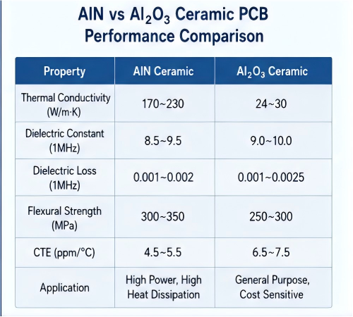
One of the defining characteristics of aluminum nitride is its thermal conductivity, which typically ranges from 170 to 230 W/m·K. This is significantly higher than alumina ceramics and approaches the performance of some metals, yet without sacrificing electrical insulation. Another key reason for its widespread use is its coefficient of thermal expansion (CTE). Aluminum nitride closely matches the CTE of silicon, making it an excellent substrate for semiconductor devices.

In addition to thermal and mechanical advantages, aluminum nitride also offers:

  • Strong dielectric strength, ensuring electrical isolation even under high voltage conditions
  • Excellent chemical stability, allowing it to perform well in corrosive environments
  • Low dielectric constant, supporting high-frequency signal integrity
  • Non-toxic composition, making it environmentally safer compared to some alternatives

These attributes make aluminum nitride an ideal material choice for ceramic PCBs used in demanding sectors such as automotive electronics, power modules, RF systems, and industrial control equipment.

Manufacturers like EBest Circuit (Best Technology) carefully select high-purity AlN powders and optimize sintering conditions to ensure consistent material performance.

What Is an Aluminum Nitride Ceramic Substrate?

An aluminum nitride ceramic substrate is the foundational layer of an AlN PCB. It is a dense, engineered ceramic plate that provides both structural support and thermal conduction for the circuit.

This substrate is produced by pressing and sintering aluminum nitride powder at high temperatures, typically above 1,800°C. During this process, the material densifies into a solid structure with minimal porosity, which is critical for achieving high thermal conductivity and mechanical strength.

The substrate itself does not conduct electricity, but it efficiently transfers heat. To create a functional circuit, conductive layers—usually copper—are bonded or deposited onto the surface. This combination forms the complete ceramic PCB.

In practical applications, the substrate plays several important roles:

  • It acts as a heat spreader, rapidly dissipating thermal energy
  • It provides mechanical stability for mounted components
  • It ensures electrical insulation between conductive layers
  • It supports fine circuit patterning for complex designs

Depending on the application, aluminum nitride substrates can be customized in terms of thickness, surface finish, and metallization type. For example, thinner substrates may be used for compact devices, while thicker ones are preferred for high-power modules requiring enhanced heat spreading.

At EBest Circuit (Best Technology), aluminum nitride ceramic substrates are engineered with tight dimensional control and excellent surface flatness. This ensures compatibility with advanced assembly processes, including wire bonding and surface mount technology.

How Is an Aluminum Nitride PCB Different from Alumina PCB?

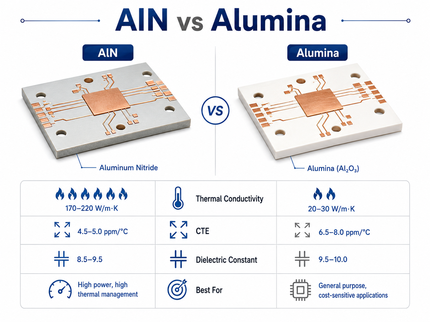
Aluminum nitride and alumina (Al₂O₃) are the two most widely used ceramic materials in PCB manufacturing. While both offer excellent electrical insulation and mechanical stability, their performance differs significantly, especially in thermal management.

Alumina has been the industry standard for many years due to its cost-effectiveness and mature manufacturing processes. However, as electronic devices become more compact and power-dense, its relatively low thermal conductivity has become a limitation.

Below is a clear comparison between the two materials:

PropertyAluminum Nitride (AlN)Alumina (Al₂O₃)
Thermal Conductivity170–230 W/m·K20–30 W/m·K
Dielectric Constant~8.5~9.8
Coefficient of ExpansionClose to siliconHigher mismatch
Mechanical StrengthHighModerate
CostHigherLower
Application FocusHigh-power, high-endGeneral purpose

While alumina remains a solid choice for many standard applications, aluminum nitride becomes the preferred option when thermal performance is critical. Engineers working on power modules, LED systems, and RF devices often find that AlN delivers measurable improvements in efficiency and reliability.

What Are the Main Benefits of Aluminum Nitride Ceramic PCB?

Aluminum nitride ceramic PCBs offer a combination of properties that directly address the challenges of modern electronic design.

Key advantages include:

  • Superior heat dissipation
    High thermal conductivity allows heat to move away from components quickly, reducing operating temperatures and extending lifespan.
  • Reliable electrical insulation
    Even under high voltage conditions, AlN maintains strong dielectric properties, ensuring safe operation.
  • Enhanced mechanical stability
    The material resists warping and deformation, even under thermal stress or mechanical load.
  • Compatibility with semiconductors
    Its CTE closely matches silicon, minimizing stress during temperature fluctuations.
  • High-frequency performance
    Low dielectric loss supports stable signal transmission in RF and microwave applications.
  • Compact design capability
    Efficient heat management enables smaller, more powerful device designs.

These advantages make aluminum nitride ceramic PCBs a strategic choice for engineers seeking both performance and reliability. EBest Circuit (Best Technology) integrates these benefits into every product by maintaining strict material selection and process control standards.

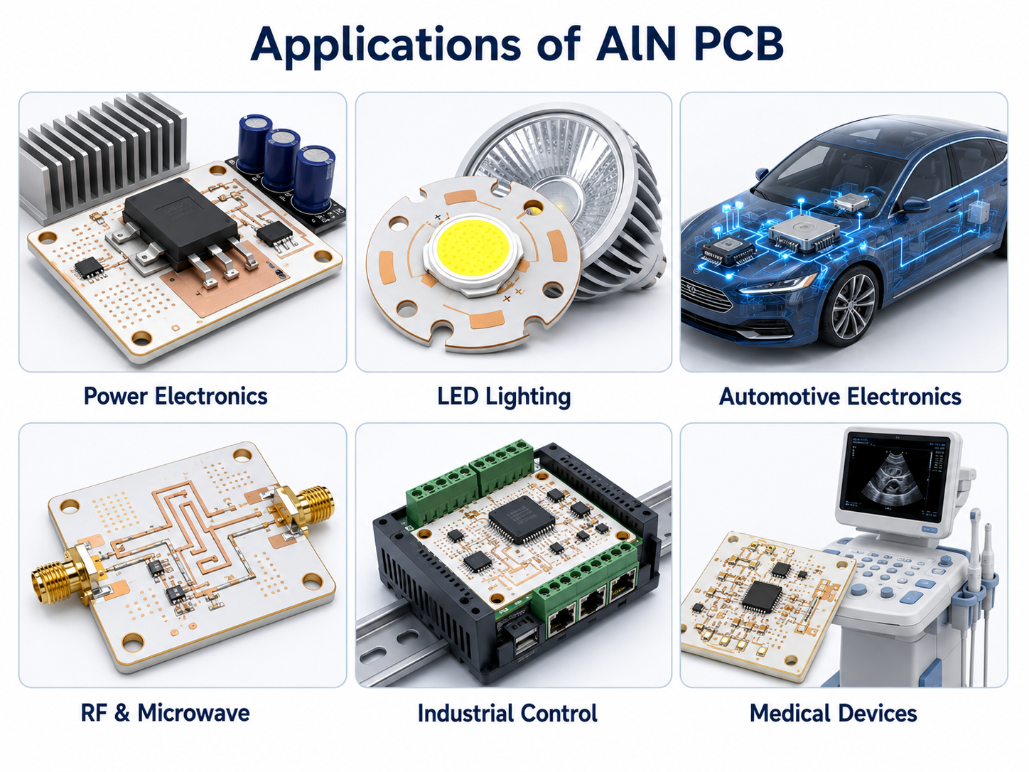
What Are Aluminum Nitride PCBs Used For?

Aluminum nitride ceramic PCBs are widely used in industries where performance, durability, and thermal management are critical. Their versatility allows them to support a broad range of advanced technologies.

Common applications include:

  • Power electronics
    Used in IGBT modules, power converters, and inverters where heat generation is significant.
  • LED lighting systems
    High-power LEDs benefit from efficient heat dissipation, improving brightness stability and lifespan.
  • Automotive electronics
    Electric vehicles and advanced driver systems require reliable thermal management under harsh conditions.
  • RF and microwave devices
    Ideal for high-frequency circuits due to low dielectric loss.
  • Industrial control systems
    Ensures stable operation in environments with fluctuating temperatures.
  • Medical devices
    Supports precision electronics where reliability is essential.

As industries continue to evolve toward higher power densities and smaller form factors, the demand for aluminum nitride PCBs is expected to grow steadily.

How Are Aluminum Nitride Ceramic PCBs Manufactured?

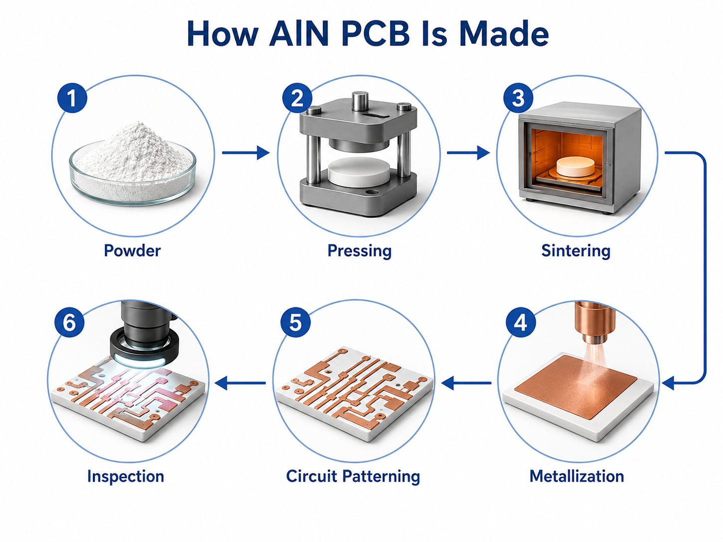
The manufacturing process of aluminum nitride ceramic PCBs is more complex than that of traditional PCBs. It requires specialized equipment and expertise to achieve consistent quality.

The process generally involves several key steps:

  • Powder preparation
    High-purity aluminum nitride powder is selected and processed.
  • Forming and sintering
    The powder is shaped and sintered at high temperatures to create a dense ceramic substrate.
  • Surface preparation
    The substrate is polished to achieve the required flatness and surface quality.
  • Metallization
    Conductive layers are applied using techniques such as Direct Bonded Copper (DBC) or Thin Film deposition.
  • Circuit patterning
    Photolithography and etching are used to define precise circuit patterns.
  • Surface finishing
    Additional coatings are applied to enhance solderability and corrosion resistance.
  • Inspection and testing
    Each board undergoes rigorous quality checks to ensure performance standards are met.

At EBest Circuit (Best Technology), advanced manufacturing capabilities ensure tight tolerances and consistent performance across all production batches. Our specialized expertise in the field of ceramic PCB manufacturing enables us to provide customized solutions for complex applications.

Can Aluminum Nitride Ceramic PCBs Support Fine Circuits?

Yes, aluminum nitride ceramic PCBs can support fine circuit patterns, especially when thin-film or advanced metallization processes are used. This capability is essential for modern electronics, where compact designs and high circuit density are increasingly common.

Fine circuit support depends on several factors, including surface smoothness, metallization method, and process control. Aluminum nitride substrates can achieve excellent surface flatness, which is critical for high-resolution patterning.

Typical capabilities include:

  • Fine line widths suitable for high-density layouts
  • Precise spacing for complex circuit routing
  • Compatibility with microelectronic assembly techniques

Thin-film technology, in particular, allows for extremely fine features, making AlN PCBs suitable for RF modules, sensors, and advanced semiconductor packaging. With proper engineering and manufacturing expertise, aluminum nitride ceramic PCBs can meet the demands of even the most intricate designs.

What Surface Finishes Are Used for Aluminum Nitride PCBs?

Surface finishes play a crucial role in ensuring reliable assembly and long-term performance. For aluminum nitride PCBs, several finishing options are available depending on the application.

Common surface finishes include:

  • ENIG (Electroless Nickel Immersion Gold)
    Provides excellent solderability and corrosion resistance.
  • ENEPIG
    Adds a palladium layer for improved wire bonding performance.
  • Immersion Silver
    Offers good conductivity and is suitable for high-frequency applications.
  • OSP (Organic Solderability Preservative)
    A cost-effective option for certain applications.

Each finish has its own advantages, and the selection depends on factors such as assembly method, environmental conditions, and performance requirements. EBest Circuit (Best Technology) offers a range of surface finishing options to meet diverse customer needs, ensuring compatibility with various assembly processes.

What Factors Affect Aluminum Nitride PCB Cost?

The cost of aluminum nitride ceramic PCBs is influenced by multiple factors, reflecting the complexity and precision required in their production.

Key cost drivers include:

  • Material quality
    High-purity aluminum nitride powder increases performance but also cost.
  • Substrate thickness and size
    Larger and thicker substrates require more material and processing time.
  • Metallization method
    Advanced techniques like DBC or thin film can significantly impact cost.
  • Circuit complexity
    Fine features and multi-layer designs require more precise processing.
  • Surface finish
    Premium finishes such as ENEPIG add to the overall cost.
  • Production volume
    Higher volumes can reduce per-unit cost through economies of scale.

While aluminum nitride PCBs are generally more expensive than standard options, their performance benefits often justify the investment. In many cases, improved reliability and thermal efficiency lead to lower total system costs over time.

EBest Circuit (Best Technology) works closely with customers to optimize design and manufacturing parameters, helping balance performance and cost effectively.

Summary:

Aluminum nitride ceramic PCBs represent a powerful solution for modern electronics that demand efficient thermal management and reliable performance. Their ability to combine high thermal conductivity with strong electrical insulation makes them ideal for high-power and high-frequency applications.

If you are exploring high-performance ceramic PCB solutions, EBest Circuit (Best Technology) is ready to support your project with advanced manufacturing capabilities and tailored engineering expertise.

For inquiries, feel free to contact: sales@bestpcbs.com

You may also like

How does a DPC Ceramic PCB Manufactured?
Saturday, July 6th, 2024

Direct Plating Copper (DPC) is a ceramic circuit board developed on the basis of ceramic film processing. Aluminum nitride/alumina ceramic is used as the substrate of the circuit, and the composite metal layer on the surface of the substrate is sputtered, and the circuit is formed by electroplating and lithography. Its basic processes are:

  • Incoming Quality Control (IQC)

The process begins with the inspection of raw materials to ensure they meet strict quality standards. This step involves checking ceramic substrates for physical defects such as cracks, chips, or surface irregularities, and verifying material properties like thermal conductivity and dielectric strength. Advanced equipment such as microscopes and X-ray fluorescence (XRF) analyzers are used for thorough inspection, ensuring only the best materials proceed to the next stage.

  • Laser Drilling

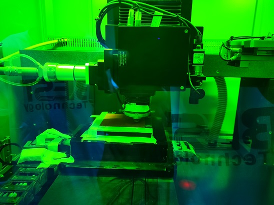
Before laser drilling, a water-soluble, food-grade substrate pigment is brushed onto the ceramic substrate to reduce reflectivity and enhance laser drilling effectiveness. After drying in an oven, a laser drilling machine is used to drill through the substrate, creating pathways for connections between the upper and lower surfaces. Depending on the ceramic material, different laser wavelengths such as infrared, green light, ultraviolet, or CO2 are used to burn away the material with each laser pulse.

How does a DPC Ceramic PCB Manufactured?
  • Laser Marking

Laser marking involves using a laser marking machine to engrave product QR codes onto the ceramic substrate. This step ensures precise and permanent identification marks on the PCB.

  • Ultrasonic Cleaning

After laser drilling and marking, the substrates are cleaned to remove any attached particles or residues. This involves coarse and fine debris removal using ultrasonic cleaning, followed by water washing to eliminate any remaining particles. The cleaned substrates undergo micro-etching to roughen the surface, enhancing the effectiveness of subsequent magnetron sputtering, and are then dried to remove surface moisture.

  • Magnetron Sputtering

In the magnetron sputtering process, a high-vacuum chamber is used to ionize argon gas, producing an ion stream that bombards a target cathode. This causes atoms of the target material to be ejected and deposited as a thin film on the ceramic substrate. Pre-sputtering treatments such as dust removal, degreasing, and slow pulling are conducted to ensure optimal results.

  • Chemical Copper Plating

Chemical copper plating thickens the copper layer, improving the conductivity of the vias and ensuring better adhesion with the sputtered copper layer. This catalytic redox reaction involves pre-treatment steps like degreasing, micro-etching, pre-immersion, activation, and acceleration to ensure proper copper deposition.

  • Full-Panel Electroplating

Full-panel electroplating increases the thickness of the copper layer. This involves processes such as degreasing, micro-etching, acid washing, copper plating, and stripping excess copper from the fixtures. The copper plating uses copper balls as anodes and an electrolyte solution of CuSO4 and H2SO4, with the primary reaction being Cu2+ + 2e- → Cu.

  • Grinding, Laminating, Exposure, and Developing

Post electroplating, the copper layer is prepared for patterning. This includes acid washing to remove oxides, grinding to roughen and clean the surface, laminating with a photoresist dry film, UV exposure through a photomask to create the desired pattern, and developing to dissolve unexposed areas, leaving behind the patterned photoresist.

How does a DPC Ceramic PCB Manufactured?

  • Pattern Plating (Electroplating Copper)

The exposed and developed areas of the substrate where the circuit pattern is defined undergo further copper electroplating to thicken the circuit traces.

How does a DPC Ceramic PCB Manufactured?
  • Etching and Stripping

Unwanted copper and dry film are removed through etching, stripping away excess copper deposited in previous steps. This includes rough grinding, film stripping, copper etching, and titanium etching, ensuring only the desired circuit pattern remains.

  • Annealing

The ceramic boards are annealed in a furnace to relieve stresses introduced during electroplating, enhancing the ductility and toughness of the copper layer and ensuring dense copper grain packing.

  • Belt Grinding

Post-annealing, the substrate surface may have an oxide layer and rough texture. Belt grinding is used to remove these oxides and smoothen the surface, ensuring the quality of subsequent gold or silver surface treatments.

  • Flying Probe Testing

High-speed flying probe testers check for continuity and shorts in the vias and circuit traces, ensuring electrical integrity.

  • Sandblasting Before Solder Mask

Prior to solder mask application, the substrate undergoes sandblasting to roughen and clean the surface, removing oxides and contaminants. This includes acid washing, sandblasting, and micro-etching.

  • Solder Mask Printing

Solder mask is printed on areas of the PCB that do not require soldering, protecting the circuits during soldering and assembly. Screen printing applies solder mask ink, which is then UV-cured and developed to remove unexposed areas.

  • Sandblasting After Solder Mask

After solder mask application, exposed areas that need surface treatments undergo sandblasting to roughen the surface and remove oxides, preparing for gold or silver plating.

  • Surface Treatment

Surface treatments like electroless or electrolytic plating of gold, silver, or other metals are applied to the solder pads, enhancing solderability and preventing oxidation.

  • Laser Cutting

Laser cutting equipment precisely cuts the finished PCBs from the manufacturing panel, ensuring accurate dimensions and clean edges.

  • Testing

Various testing equipment, including thickness gauges, Automated Optical Inspection (AOI) machines, and ultrasonic scanning microscopes, are used to inspect the PCBs’ performance and appearance, ensuring they meet quality standards.

  • Packaging and Shipping

Finally, the PCBs are vacuum-packed using packaging machines to protect them during transport. They are then stored and shipped to customers, ensuring they arrive in perfect condition.

Above is the all the processes of DPC muanufacturing. If you are interested in process of other PCBs, welcome to contact us.

You may also like