PCB manufacturing PCB manufacturing
Home > Blog

Medical Device PCB Assembly Canada Quote for OEM Projects

August 31st, 2026

Medical device PCB assembly Canada is usually searched by buyers who already have a real project, not by readers who only want a definition. A medical electronics team may already have Gerber files, a controlled BOM, approved components, test requirements, and a delivery target. What they need next is a PCBA partner that can review the build, protect component traceability, control soldering quality, and give a clear quote path before production starts.

EBest Circuit supports Canada medical device and medical electronics buyers as a China-based PCB and PCBA manufacturing partner. For projects that need PCB fabrication, component sourcing, SMT assembly, through-hole assembly, inspection, testing support, and documented production control under one workflow, our team can review the files and confirm whether the build is suitable for prototype, small-batch, or follow-up production.

medical device PCB assembly Canada
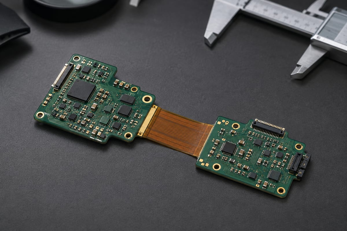
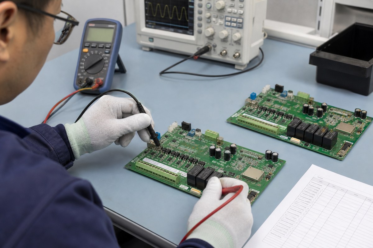
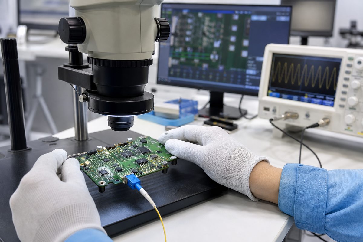
Medical device PCB assembly Canada support for OEM PCBA projects.

Medical Device PCB Assembly Canada Suppliers for OEM PCBA Quotes

Canada buyers usually compare several supplier types before sending a medical PCBA RFQ. A local supplier may fit projects that need domestic communication, short regional shipping, or local program management. An overseas PCBA partner may fit projects that need broader PCB fabrication capability, flexible component sourcing, prototype-to-production support, or more cost-controlled manufacturing.

For a Canada medical electronics project, a practical supplier shortlist can include local PCB assembly shops, EMS providers, ISO 13485-related manufacturing partners, and overseas PCB/PCBA manufacturers that serve Canada customers.

Supplier buyers may compare Simple review angle
MIS Electronics Ontario EMS with PCB assembly, testing, packaging, and medical-market experience
R.S. Electronique Montreal PCB assembly option for prototypes and production runs
JLS Electronic Technologies Montreal EMS supplier for PCB assembly, prototypes, and production
STIM Canada Toronto-area EMS provider for PCBA, box-build, NPI, and medical projects
Vexos Markham Canada EMS facility for high-mix, complex OEM manufacturing
RMF Design and Manufacturing Canadian design and manufacturing partner with medical project experience
Servetronics Ontario PCBA supplier for SMT, THT, BGA, coating, and functional test needs
Gen Pack Assembly Hamilton electronics assembly supplier serving medical and healthcare applications
Canadian Circuits Canada PCB manufacturer with PCB assembly and medical-industry coverage
Dynamic Source Manufacturing Canada/USA EMS provider supporting medical electronics and health-tech projects

For an OEM quote, the useful question is not only “Who is nearby?” It is “Who can review this medical PCBA package accurately and reduce production risk before SMT?”

Before choosing a supplier, buyers should check whether the supplier can review:

  • Gerber files, stackup, drill files, and fabrication notes
  • BOM with MPN, manufacturer, approved alternatives, and lifecycle status
  • CPL / pick-and-place file, polarity marks, and assembly drawings
  • Critical components such as BGA, QFN, fine-pitch ICs, connectors, sensors, and medical-grade parts
  • Required inspection, test, traceability, and packaging documents
  • Prototype quantity, pilot quantity, target build date, and delivery urgency

PCB Assembly Canada vs China PCBA Partner for Medical Projects

For medical electronics projects, Canada and China suppliers can both be reasonable choices. The better decision depends on the project stage, BOM risk, required documentation, delivery plan, and whether the buyer wants a local supplier or an integrated manufacturing route.

Buyer priority Canada supplier fit China PCBA partner fit
Communication Local meetings Fast engineering review
Supply chain Local vendor control PCB + sourcing + PCBA in one flow
PCB complexity Simple or approved boards HDI, rigid-flex, RF, MCPCB, heavy copper
Components Parts already local BOM sourcing or partial turnkey
Cost Domestic cost acceptable Better pilot or repeat-build cost
Documentation Existing local approval Traceability and inspection records

EBest Circuit is not a Canada local factory. We are a China-based PCB and PCBA manufacturer serving Canada and global buyers. The value is not local geography; the value is integrated manufacturing capability, engineering review, component sourcing support, documented production control, and responsive communication for buyers who are comfortable with overseas manufacturing.

Medical PCB Assembly Requirements for Canada RFQ Review

Medical PCB assembly requires a cleaner RFQ package than many consumer electronics projects. Small mistakes can create expensive rework, validation delays, or field reliability risks. Before quoting, EBest Circuit reviews whether the PCB data, BOM, assembly files, and inspection requirements are complete enough for production evaluation.

For Canada medical device buyers, the RFQ should make production risk visible early. The supplier should not only quote unit price. It should also flag missing drawings, unclear polarity, package mismatch, insufficient component quantity, difficult replacement parts, special process notes, and inspection requirements that may affect lead time.

Useful RFQ details include:

  • Intended use, prototype or production stage, and target quantity
  • PCB type, layer count, copper weight, surface finish, and special material
  • Soldering requirements for SMT, THT, mixed assembly, or hand soldering
  • Sensitive components, date-code requirements, and approved sourcing channels
  • Test method, fixture availability, firmware loading, and functional acceptance criteria
  • Required documents such as inspection records, test records, COC, or traceability data

When these details are clear at the RFQ stage, the buyer can compare suppliers based on real project fit instead of a low quote that changes after engineering review.

Medical Device PCB Assembly Manufacturer Capability at EBest Circuit

EBest Circuit can support medical device PCB assembly projects that require PCB fabrication and PCBA under one manufacturing route. This is useful for buyers who do not want to split bare board production, component purchasing, SMT assembly, inspection, and delivery control across too many suppliers.

Capability item EBest Circuit capability
Assembly services Consigned, full turnkey, partial turnkey
Assembly type SMT, THT, mixed assembly
Minimum SMD component 01005
Minimum BGA pitch 0.25 mm
Bare board size 0.2 x 0.2 in to 20 x 20 in / 22 x 47.5 in
Component packages Reel, cut tape, tube, tray, loose parts
Placement capacity 13,200,000 chips/day

For medical electronics, this capability matters because the PCB is often not a simple board. A project may include fine-pitch ICs, connectors, sensors, thermal requirements, tight board space, coating or cleaning notes, controlled soldering conditions, and test points that need to be understood before assembly starts.

EBest Circuit can also review PCB product types often used in medical electronics, including FR4 PCB, HDI PCB, rigid-flex PCB, FPC, ceramic PCB, metal core PCB, high-frequency PCB, and heavy copper PCB. If the project combines a special PCB structure with PCBA, one engineering review can reduce handoff risk.

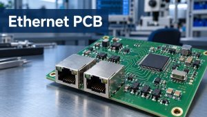
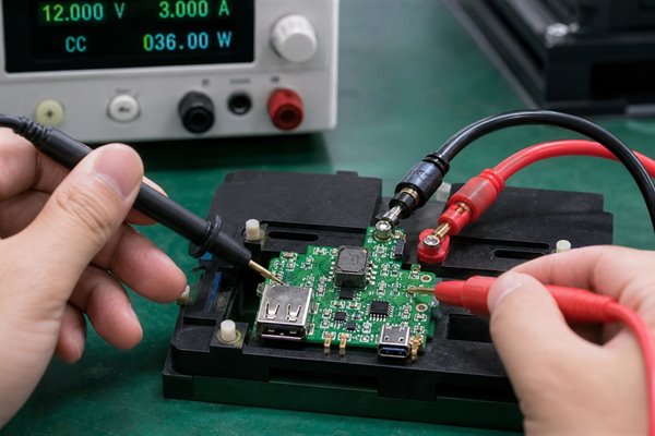
medical device PCB assembly Canada
SMT production capacity helps Canada medical electronics buyers review project fit.

ISO 13485 PCB Assembly and Traceability for Canada Medical Buyers

For medical device supply chains, ISO 13485 is not just a logo on a page. Buyers need to know whether production data, material information, process records, inspection results, and changes can be controlled in a way that supports regulated project requirements.

For buyers who need quality-system alignment, EBest Circuit can support discussions around ISO 13485:2016, ISO 9001:2015, IATF 16949, AS9100D, UL, RoHS, and REACH. For a Canada medical buyer, the useful next step is to confirm the certificate scope, project requirements, and records needed for the specific PCB or PCBA order.

Traceability should be discussed before production, especially when the BOM includes critical ICs, customer-supplied components, approved manufacturer lists, or date-code requirements.

Traceability item Buyer value
PCB lot Batch link
MPN / date code / lot code Material control
Incoming inspection Parts verified
SMT records Process history
AOI / X-Ray / visual inspection Soldering evidence
Final inspection Pre-shipment check
Deviation records Controlled changes

For medical PCB assembly, this gives the buyer more than finished boards. It gives the buyer a clearer production history to review when quality, validation, or repeat orders matter.

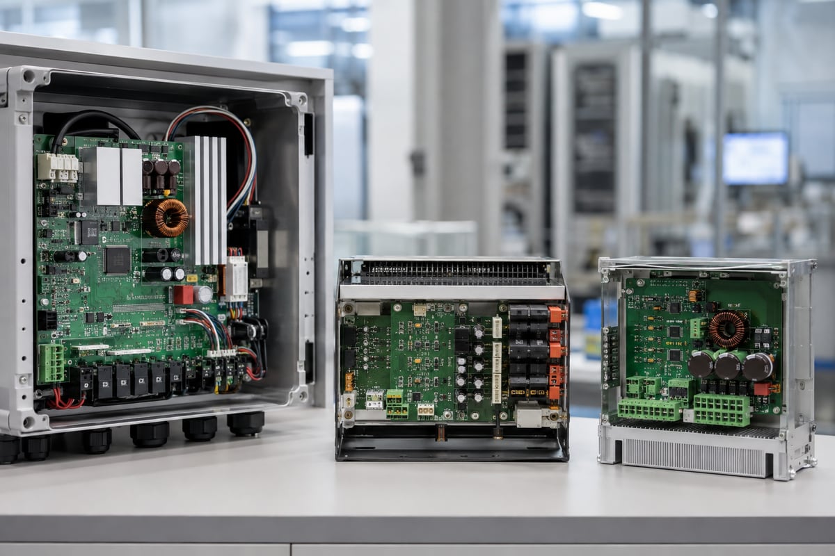
medical device PCB assembly Canada
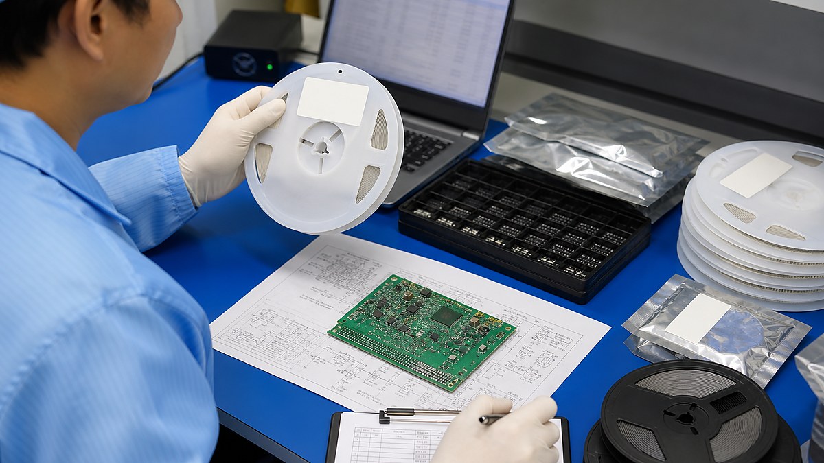
Component receiving and BOM review support traceable medical PCBA production.

Medical PCB Assembly Services for Quality-Controlled Production

The quality risk in medical PCB assembly is often not one dramatic failure. It is a collection of small problems: polarity error, wrong MPN, insufficient solder, hidden BGA defect, flux residue, connector fit issue, unclear test method, or an unrecorded change.

EBest Circuit builds the PCBA process around prevention first: file review, DFA checks, incoming inspection, controlled SMT/THT assembly, solder paste printing, SPI, placement, reflow, AOI / X-Ray inspection, functional testing support, final inspection, cleaning, drying, packaging, and delivery.

For buyers, the most useful controls include 3D SPI, Yamaha SMT placement, FAI, nitrogen reflow, wave soldering, 3D AOI, and X-Ray inspection.

Buyer concern Production control to confirm
Wrong part or polarity BOM / CPL / FAI checks
Fine-pitch soldering SPI + placement + AOI
BGA / QFN joints X-Ray when required
Mixed assembly SMT + THT route
Functional risk Test criteria review
Repeat issues CAPA and records

When the supplier can answer these questions with process records, the buyer has more confidence than with a simple “we can assemble it” statement.

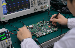
medical device PCB assembly Canada
Inspection controls help reduce soldering and assembly risk before shipment.

Medical Electronics Manufacturing Services for Canada OEM Supply Chains

Many Canada medical electronics buyers do not only need soldering. They need a supply chain path that can keep the project moving when the BOM changes, components become difficult to buy, or a prototype becomes a pilot build.

EBest Circuit can support medical electronics manufacturing services around the PCBA build, including BOM review, component sourcing, customer-supplied parts coordination, partial turnkey support, PCB fabrication, SMT assembly, THT assembly, inspection, and testing coordination.

When EBest Circuit sources components, the preferred route is through manufacturers or authorized distributors such as DigiKey, Mouser, Future, TTI, Avnet, and Arrow. If a part is unavailable, engineering can review alternatives for buyer approval instead of making uncontrolled substitutions.

Supply chain question What the buyer should clarify
Turnkey or partial turnkey? Source vs supplied list
Customer-supplied ICs? MPN, quantity, package, date code
Shortage or obsolete parts? Approved alternatives
Medical BOM control? AML and substitution rules
Repeat builds? Forecast and change control

The goal is not to push every buyer into full turnkey. The goal is to give the buyer a controlled route for the BOM situation they actually have.

Medical Device PCB Assembly Canada Lead Time at EBest Circuit

Lead time for medical device PCB assembly depends on file readiness, PCB complexity, BOM availability, test requirements, coating or cleaning requirements, and whether the build is consigned, turnkey, or partial turnkey. A supplier should make these dependencies clear before the buyer commits.

For a quick schedule check, EBest Circuit gives buyers a practical PCBA reference: typical PCBA production can be 1-5 days, normal PCBA service is about 1 week, and the fastest PCBA service can be 2 days when the project is suitable. These timelines apply after the required files, bare boards, components, and engineering confirmations are ready.

Project situation What affects the schedule
Consigned parts Receiving check
Full turnkey BOM Parts availability
Prototype PCBA File readiness
Medical validation Records + testing
Urgent pilot run Fastest-service review

For Canada buyers, the best lead-time conversation starts before the order is placed. Send the BOM, Gerber files, CPL, quantity, and test requirements first. EBest Circuit can then confirm whether the project fits normal PCBA lead time, fastest service, or a longer schedule because of sourcing, documentation, or test requirements.

Medical Device PCB Assembly Case Study for a Canada Buyer

A Canada medical electronics buyer needed a small PCBA build for a sensor-control module used in a regulated device project. The buyer had Gerber files, BOM, CPL, assembly drawings, and several approved critical components, but the project could not move to assembly until the BOM and component status were checked.

Stage Issue EBest Circuit action Buyer value
Before production Unclear passive alternatives BOM note review Less substitution risk
Before SMT Connector footprint risk Package check Lower mismatch risk
Material review Critical IC control Part verification Less shortage risk
Assembly Soldering risk FAI, SPI, AOI, X-Ray Better process control
After assembly Record need Inspection records Easier repeat review

This is the type of value a Canada buyer should look for in medical device PCB assembly: not only low assembly cost, but fewer uncontrolled risks between RFQ, production, testing, and repeat orders.

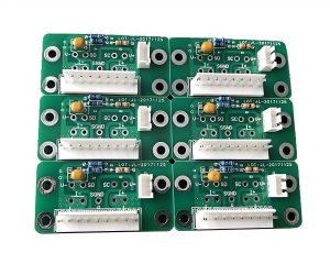
medical device PCB assembly Canada
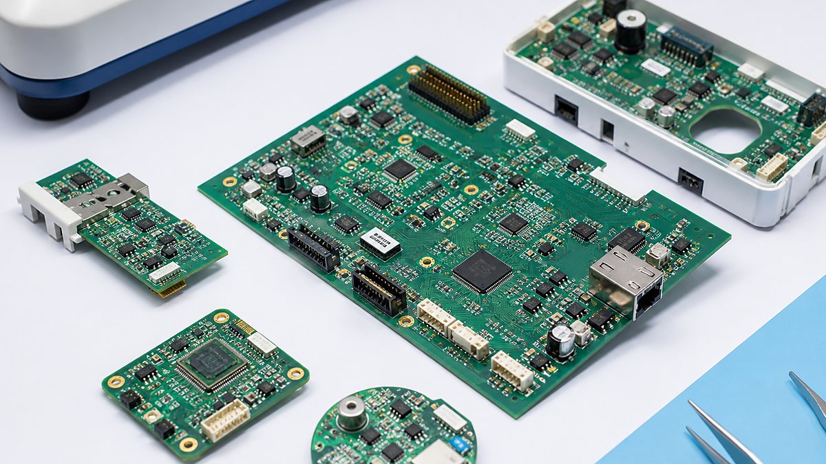
Medical PCBA samples can be reviewed for prototype, pilot, and repeat-build planning.

FAQs About Medical Device PCB Assembly Canada

Is EBest Circuit a Canada medical device PCB assembly factory?

No. EBest Circuit is a China-based PCB and PCBA manufacturer serving Canada and global buyers. Canada buyers can use EBest Circuit when they want overseas PCB fabrication, component sourcing, SMT assembly, inspection, testing support, and traceability under one supplier route.

Can EBest Circuit support ISO 13485 PCB assembly projects?

EBest Circuit can support ISO 13485:2016-related quality discussions for medical PCB and PCBA projects. Buyers should confirm the certificate scope, project requirements, documentation needs, and inspection records before placing an order.

What files should I send for a medical PCBA quote?

Send Gerber files, BOM, CPL / pick-and-place file, assembly drawings, quantity, test requirements, component sourcing preference, special process notes, and required quality documents. If some information is missing, EBest Circuit can review the package and point out what needs confirmation.

Can EBest Circuit assemble customer-supplied medical components?

Yes, consigned assembly can be discussed. The buyer should provide MPN, quantity, packaging, date-code requirements, and approved usage notes. EBest Circuit can check receiving and production readiness before SMT.

Can EBest Circuit source components for medical electronics projects?

Yes. EBest Circuit can support full turnkey or partial turnkey sourcing, using manufacturers or authorized distributors when available. Substitutions should be reviewed and approved by the buyer before production.

What inspection is available for medical PCB assembly?

Inspection may include incoming component checks, SPI, FAI, AOI, X-Ray, visual inspection, final inspection, and testing support depending on the build. BGA, QFN, and hidden solder joints should be discussed during RFQ review.

How fast can EBest Circuit deliver medical device PCB assembly for Canada buyers?

PCBA lead time depends on BOM readiness, PCB availability, assembly complexity, inspection requirements, and shipping. For suitable projects, EBest Circuit can review whether the build fits 1-5 day PCBA production or the fastest 2-day PCBA service.

How do I start a medical PCB assembly quote?

Send your Gerber files, BOM, CPL, assembly drawings, quantity, target schedule, and test requirements to sales@bestpcbs.com. For early review, you can send the BOM and PCB files first, and EBest Circuit will help check whether the project is ready for quotation and production planning.

Canada medical device buyers can use medical device PCB assembly Canada as a practical supplier-selection topic: compare local convenience, overseas PCBA capability, certification fit, BOM support, testing requirements, and lead time before choosing a manufacturing route. If your project needs PCB fabrication, component sourcing, SMT assembly, inspection, and testing support under one workflow, EBest Circuit can review your files and confirm the next RFQ step.

You may also like

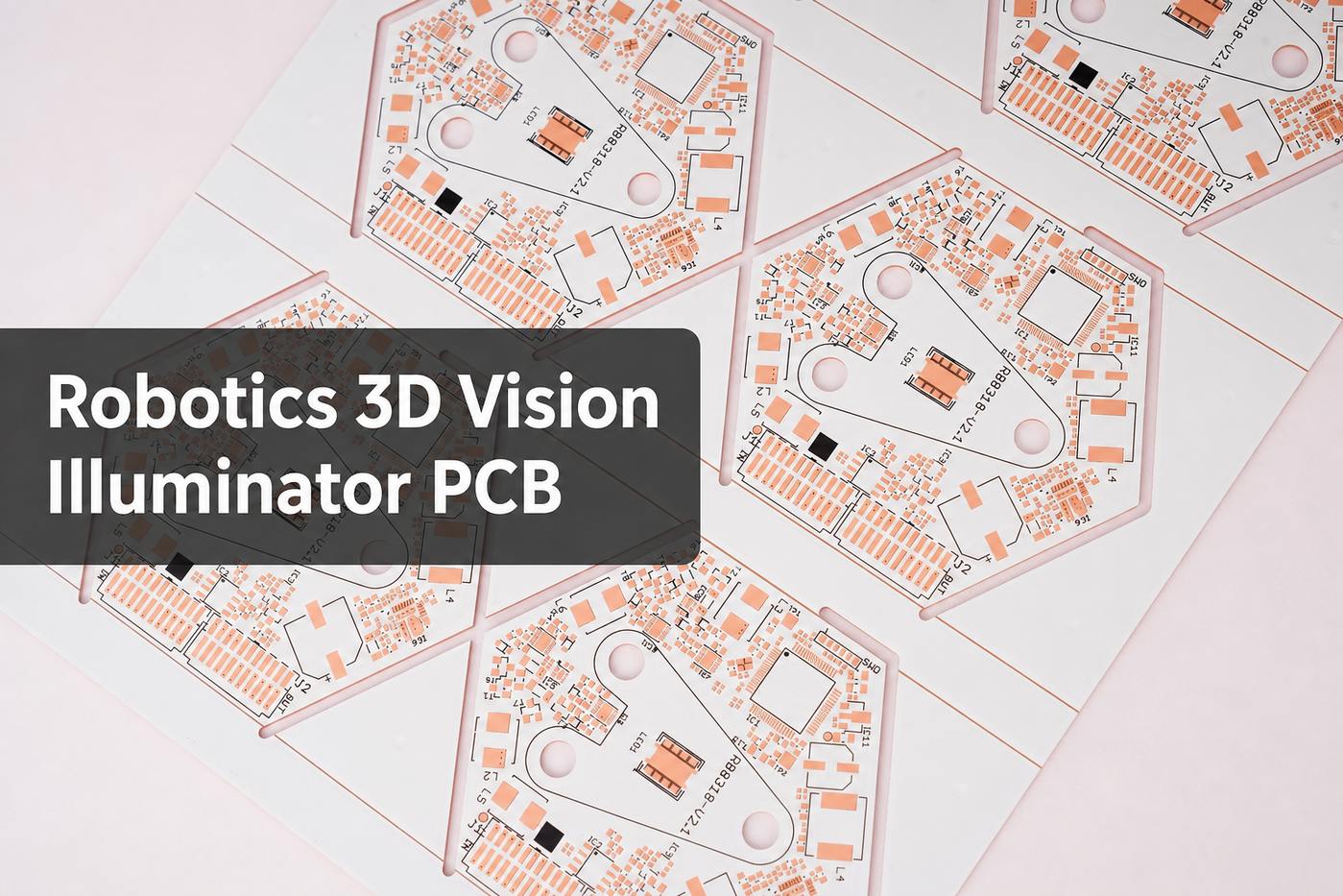
Top Robotics 3D Vision Illuminator PCB Manufacturers in Germany

August 27th, 2026

Top robotics 3D vision illuminator PCB manufacturers in Germany support lighting hardware that helps cameras capture stable depth data on reflective, dark, textured, or fast-moving objects. Choosing a supplier is not simply a matter of finding a company that can produce an aluminum PCB: the board must carry the LED load, remove heat, preserve optical consistency, fit the mechanical assembly, and arrive in time for camera and robot validation.

This guide helps German buyers assess manufacturers, prices, lead times, thermal capabilities, and sourcing routes for an illuminator PCB project. Buyers who also need a China manufacturing option can work with EBest Circuit, founded in 2006 and supported by 160 employees, more than 20 years of PCB and PCBA experience, 1,800+ customers across 40 countries, and a reported 97% on-time delivery rate. Its service combines PCB fabrication, component sourcing, PCBA, and testing. Send your Gerber files, BOM, target quantity, and required delivery date to sales@bestpcbs.com for an initial engineering review.

robotics 3D vision illuminator PCB

What Is a Robotics 3D Vision Illuminator PCB?

A 3D vision illuminator PCB is the circuit board that supports and drives the light source used by a robotic vision system. Depending on the sensing method, the illuminator may project infrared flood light, a structured pattern, a line, or synchronized pulses. The camera records the reflected light so that the vision system can calculate depth, locate parts, inspect surfaces, or guide a robot.

The PCB may look simple because LEDs dominate the visible side of the assembly, but its performance affects the complete optical system. Uneven LED current can create inconsistent brightness. Poor heat spreading can shift wavelength, reduce light output, shorten LED life, or distort calibration. Mechanical error can move the emitting surface away from the intended optical axis.

A buyer should therefore define the illuminator as an electro-optical assembly rather than as a generic LED board. Important inputs include:

  • illumination wavelength and optical power;
  • continuous, strobed, or pulsed operating mode;
  • LED quantity, package, current, and forward voltage;
  • required thermal resistance and maximum junction temperature;
  • board outline, mounting holes, connector position, and height restrictions;
  • driver topology, synchronization signals, and protection circuits;
  • camera distance, field of view, enclosure, lens, diffuser, or projector interface;
  • operating temperature, vibration, contamination, and service-life targets.

MCPCB is often suitable when the main challenge is removing heat from a compact LED array. A more complex illuminator may instead need a multilayer FR-4 board, a hybrid construction, or separate LED and control boards. The correct choice depends on the thermal path, signal requirements, component density, and mechanical design.

robotics 3D vision illuminator PCB

Top 3D Vision Illuminator PCB Manufacturers in Germany

The following companies are worth evaluating for thermal, high-reliability, prototype, or advanced PCB requirements in Germany. Their available services fit parts of an illuminator PCB project, but buyers should still confirm the MCPCB construction, PCBA scope, optical testing, available capacity, and production location for each quotation.

CONTAG AG, Berlin: CONTAG manufactures IMS and metal-core PCBs for LED, industrial, automotive, energy, and other thermally demanding applications. It also offers multilayer, HDI-SBU, high-frequency, flex, and rigid-flex boards. It is a strong candidate when an illuminator requires thermal engineering support, a fast German prototype, or a hybrid solution rather than a basic one-layer aluminum board.

Unimicron Germany GmbH, Geldern: Unimicron Germany offers multilayer boards up to 24 layers, HDI, high-frequency technology, metal-inlay solutions, IMS/heatsink technology, and other heat-management options. The company serves industrial and robotics applications, making it relevant when an illuminator combines power, control, communication, and thermal functions.

Becker & Müller Schaltungsdruck GmbH, Steinach: Becker & Müller provides in-house German production for prototypes and small batches and keeps IMS, FR-4, high-Tg, HF, and flex materials in stock. Its express service covers one- and two-sided boards, multilayers, and rigid-flex products. Buyers should ask which delivery option applies to the selected IMS material and stack-up.

Hotoprint Elektronik: Hotoprint manufactures PCBs in Germany, including multilayers up to 12 layers, flexible, rigid-flex, semiflex, and aluminum boards. Prototype and express services can begin from three working days, although the actual delivery date depends on the final MCPCB specification.

Leiton GmbH, Berlin: Leiton offers aluminum and copper IMS boards, German prototype production, an online calculator, and custom quotation support. Its Copper-IMS guide lists different lead-time options by layer count and shows which constructions require a direct enquiry.

This shortlist should begin a technical comparison, not end it. Some German companies focus mainly on bare PCBs, while a robotics buyer may need component sourcing, LED bin management, SMT assembly, programming, and functional testing. Ask each supplier to state exactly which operations are included and where they will be performed.

3D Vision Illuminator PCB Prices in Germany: What Buyers Should Compare

There is no reliable standard market price for a custom 3D vision illuminator PCB. Two boards with the same outline can have very different costs because price depends on material, panel utilization, copper weight, thermal dielectric, layer count, surface finish, tolerances, testing, quantity, and delivery speed.

For MCPCB prototypes, the main price drivers normally include:

  • aluminum versus copper base;
  • standard versus high-performance thermal dielectric;
  • one-layer, two-layer, or multilayer IMS construction;
  • board thickness and copper weight;
  • routed outline, slots, countersinks, or tight mechanical tolerances;
  • white solder mask, special marking, ENIG, or another nonstandard finish;
  • electrical test, documentation, and expedited manufacturing;
  • assembly quantity, LED package, placement density, and test coverage.

The lowest bare-board price is not always the lowest project cost. A cheaper board can become expensive if it needs a separate assembler, additional incoming inspection, repeated engineering communication, or rework after thermal testing. Conversely, paying a German prototype premium may be justified when local engineering contact or a very short iteration loop prevents a delayed robot trial.

Request quotations with the same manufacturing package and commercial assumptions. Each RFQ should specify quantity, panelization responsibility, material, copper, surface finish, test scope, tooling, delivery term, destination, and whether freight and tax are included. If PCBA is required, compare the BOM price, approved component sources, alternates, setup charges, programming, functional testing, and packaging separately.
A practical comparison uses at least three totals: prototype cost, landed cost, and cost of the next production quantity. This prevents an attractive sample price from hiding an unsuitable scale-up model.

What Lead Times Do German Manufacturers Offer for 3D Vision Illuminator MCPCBs?

German manufacturers publish useful benchmarks, but buyers must distinguish manufacturing time from delivery to the project site. The clock may begin only after data approval, material confirmation, DFM closure, and order release.

Leiton’s Copper-IMS technology document dated May 26, 2025, provides the clearest layer-specific public reference:

Copper-IMS constructionOnline calculationStandard on explicit enquiry
1 layer12 working days5 working days
2 layersNot availableFrom 4 working days
4-6 layersNot availableFrom 5 working days

These are Leiton’s manufacturing options for Copper-IMS boards. They are not universal German market lead times and do not automatically include assembly or shipping.

Eurocircuits lists five working days for bare boards and ten working days for assembled boards in its one-layer aluminum IMS pool. Because its PCB and assembly services are handled by factories in Germany and Hungary, buyers who require production specifically in Germany should confirm the assigned plant.

For project planning, separate the schedule into five parts:

  1. DFM review and clarification;
  2. special-material or component procurement;
  3. bare-board fabrication;
  4. assembly, programming, and functional testing;
  5. packing and transport to the German destination.

An advertised four- or five-day build does not help if a selected LED has a six-week procurement lead time. Send the complete BOM and approved-alternate policy early, and ask the supplier to state the ready-to-ship date rather than only the fabrication cycle.

Germany vs China for Robotics 3D Vision Illuminator PCB Manufacturing

Germany and China should not be compared through a single price or speed claim. The better choice depends on the development stage, specification stability, order quantity, communication needs, supply chain, and required manufacturing scope.

Buyer priorityGermanyChina
Local iterationStrong fitRemote review required
Integrated PCBASupplier-dependentCommonly available
Repeat-volume costQuote-dependentOften competitive
TransportShorter regional routeAdd freight and customs
Best useUrgent local prototypesIntegrated builds and scaling

A sensible sourcing strategy may use German manufacturing for an urgent local iteration and an approved China partner for integrated PCBA or repeat volume. Compare both options using the same material, stack-up, tolerances, surface finish, inspection scope, Incoterm, and delivery destination. If two sources will be used, approve the same golden sample before transfer.

Which MCPCB Process Capabilities Does EBest Circuit Offer for Robotics 3D Vision Illuminators?

For illuminator projects, EBest Circuit supports the following metal-base PCB production ranges:

ItemStandard capabilitySpecial capability
Thermal conductivity1-3 W/(m·K)3-8 W/(m·K), subject to material confirmation
Board constructionSingle-sided, double-sided, single-sided two-circuit-layer aluminum/copper baseSingle-sided four-layer, subject to review
Thermoelectric separationCopper-base PCBCopper-aluminum composite construction
Inner-layer copper0.5-3 oz4 oz or above, subject to review
Outer-layer copper1-3 ozAbove 3 oz, subject to review
Processing thickness0.8-3.0 mm4.0 or 5.0 mm by material order; bendable aluminum: 0.4-1.0 mm
Maximum aluminum-board size480 × 1180 mmSingle-sided aluminum: 1600 × 480 mm

Final capability depends on the complete files, material availability, and quantity.

robotics 3D vision illuminator PCB

What Lead Times Does EBest Circuit Offer for Robotics 3D Vision Illuminator PCBs?

For standard MCPCB prototypes below one square meter, buyers can use the following fabrication times as an initial planning reference. The confirmed schedule depends on the released specification and current capacity.

MCPCB layersNormal serviceFastest service
1 layer4 days24 hours
2 layers14 days168 hours
4 layers21 daysConfirm before ordering

These timings apply to standard MCPCB prototypes with a total order area below one square meter. The standard specification uses conventional aluminum material, 0.8-2.0 mm board thickness, 0.5 oz or 2 oz copper, lead-free HASL, white solder mask, black silkscreen, and nominal thermal conductivity of 0.8 W/(m·K).

High-conductivity materials, thermoelectric-separation copper-base PCBs, OSP, special copper weights, unusual thicknesses, tight tolerances, and nonstandard panel requirements need a project-specific schedule. Production timing begins after the manufacturing data, material choice, technical questions, and commercial terms are confirmed.

The table covers bare-board production only. Component purchasing, PCBA, functional testing, packing, international freight, customs clearance, and delivery within Germany must be added separately. If the project deadline is fixed, send the files and required arrival date to sales@bestpcbs.com so EBest Circuit can check current capacity and provide a realistic ready-to-ship schedule.

EBest Circuit Engineering Case: Building a Robotics 3D Vision Illuminator PCB

In a robotics 3D vision system, the illuminator must project repeatable light while the camera captures depth information. If heat builds up unevenly beneath the LED array, brightness can drift across the field of view and make optical calibration less stable. The PCB therefore acts as part of the lighting system, not just as a carrier for LEDs.

For one German illuminator project, EBest Circuit manufactured 180 pieces of a single-sided, two-circuit-layer thermoelectric-separation copper-base PCB. Its direct thermal path moved heat from the LED mounting area into the 1.5 mm copper base, while the isolated circuit layer carried power to the emitters. The specified 3 W/(m·K) material and 1 oz / 1 oz copper were selected to balance heat removal, current distribution, and the required 1.6 mm ±10% finished thickness.

The confirmed production specification was:

  • 1.5 mm copper base;
  • 1 oz / 1 oz copper;
  • thermal conductivity of 3 W/(m·K);
  • finished board thickness of 1.6 mm ±10%;
  • white solder mask and black silkscreen;
  • OSP surface finish;
  • delivery according to the customer’s panel drawing, with each individual board retaining its specified process rails.

White solder mask kept the LED side visually clean, black legend made polarity and assembly marks easy to identify, and OSP provided a flat surface for LED soldering. The boards were delivered in the customer’s released panel format with the required process rails, allowing the panels to enter LED assembly without repanelization.

Before production, the customer approved the final board configuration and panel format. The completed 180-piece lot was supplied with the requested COC and electrical test report. The German team therefore received one consistent board build for LED assembly and later camera-and-illuminator validation, without having to reconcile different thermal, mechanical, and panel specifications after delivery.

Why Choose EBest Circuit for 3D Vision Illuminator PCB Manufacturing?

EBest Circuit is a China-based PCB and PCBA manufacturing partner serving German and international buyers. Founded in 2006, the company has more than 20 years of industry experience, 160 employees, 1,800+ customers across 40 countries, and a reported 97% on-time delivery rate. It is most relevant when the project needs more than a bare-board price.

Technical support around the buyer: One sales contact is supported by three technical team members. DFM review, BOM optimization, and process-fit suggestions are available from engineers with long PCB and PCBA experience.

One project scope from board to test: PCB fabrication, component sourcing, PCBA, and customer-defined testing can be coordinated together, reducing handoffs between unrelated suppliers.

Prototype and low-volume support: Engineering samples and small batches help teams verify thermal behavior, mechanical fit, assembly, and optical performance before scaling.

Factory and supply-chain coverage: In-house PCB and PCBA resources are supported by more than 1,000 supply-chain partners, helping coordinate materials, components, quality controls, and delivery.

Traceability and quality systems: The digital workshop can trace material and product batches, production cycles, and progress. Available quality certifications include ISO 9001, ISO 13485, IATF 16949, and AS9100D.

A German manufacturer may still be preferable when physical production in Germany or immediate local iteration is mandatory. EBest Circuit is a stronger candidate when the buyer values integrated China sourcing, technical support, coordinated PCBA, traceability, and a route from prototypes to repeat production.

What Should You Send EBest Circuit for a 3D Vision Illuminator PCB Quote?

A first quotation does not need a perfect document package. To let EBest Circuit understand the project and identify missing information, start with five essentials:

  • your Gerber or ODB++ data, plus the board outline;
  • the LED or PCBA BOM if assembly is required;
  • prototype and expected production quantities;
  • known thermal targets, such as base material, conductivity, copper weight, or heatsink interface;
  • the German delivery location and the date the boards or assemblies are needed.

If your files are not complete yet, that is fine. Send what you have, and the engineering team will identify the few details needed next to evaluate price, manufacturability, thermal performance, and lead time. You do not need to prepare the full production package before requesting an initial review.

Email the available files to sales@bestpcbs.com and state that the request is for a robotics 3D vision illuminator PCB. EBest Circuit will review the current design, explain any information still needed, and prepare the quotation around your actual development stage.

FAQs About Robotics 3D Vision Illuminator PCB

Should a 3D vision illuminator use an aluminum or copper-base PCB?

Aluminum MCPCB is often suitable for cost-controlled LED heat spreading. Copper-base and thermoelectric-separation constructions can provide a more direct thermal path for higher heat density or tighter thermal targets. The right choice depends on LED power, pulse conditions, dielectric performance, mechanical structure, and the heatsink interface.

Can German manufacturers provide fast MCPCB prototypes?

Yes. Some German suppliers offer express or short prototype services. Leiton lists a five-working-day option for a one-layer Copper-IMS construction by direct enquiry, while more complex constructions require confirmation. Always check when the production clock begins and whether assembly and transport are included.

What should buyers compare besides the quoted PCB price?

Compare the metal base, dielectric, thermal conductivity, copper weight, board thickness, surface finish, tolerances, electrical test, documentation, tooling, panel delivery format, freight, and tax. For PCBA, also compare component sources, assembly setup, programming, functional testing, and approved alternatives.

Does EBest Circuit manufacture thermoelectric-separation copper-base PCBs?

Yes. EBest Circuit manufactures thermoelectric-separation copper-base PCBs. One completed German customer order used a single-sided, two-circuit-layer construction with a 1.5 mm copper base, 1 oz / 1 oz copper, 3 W/(m·K) thermal conductivity, OSP, and a finished thickness of 1.6 mm ±10%.

How can a German buyer reduce risk when sourcing an illuminator PCB from China?

Release a complete manufacturing package, approve the production data before fabrication, define acceptable materials and substitutions, agree on inspection and test reports, confirm the shipping term, and approve the pilot or golden sample before repeat production. These controls make the comparison more reliable than selecting a supplier by unit price alone.

Have a robotics 3D vision illuminator PCB ready for review? Email the available files, quantity, thermal requirements, and German delivery target to sales@bestpcbs.com. EBest Circuit will check the design, clarify the key manufacturing decisions, and respond with a quotation and project-specific schedule.

You may also like

Car Charger Circuit Board Manufacturing and Assembly for USB-A, USB-C and USB PD Modules

August 27th, 2026

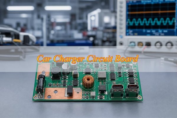
A car charger circuit board converts vehicle power into a stable USB output while protecting the connected device and managing charging behavior. The car charger circuit board combines an input protection stage, a DC-DC power stage, a charging or USB controller, filtering and the output connector in a compact space. This article covers low-voltage automotive USB charging modules used in plug-in, dashboard and center-console products, not EV traction-battery or onboard chargers.

The practical challenge is not simply making the USB port turn on. An automotive USB charger PCB must carry the required current without excessive voltage drop, remove heat from the switching components, survive the specified electrical environment and keep the connector mechanically stable. If your design files are ready, send the Gerber or ODB++, BOM, schematic, mechanical data and test requirements to sales@bestpcbs.com for a free DFM review.

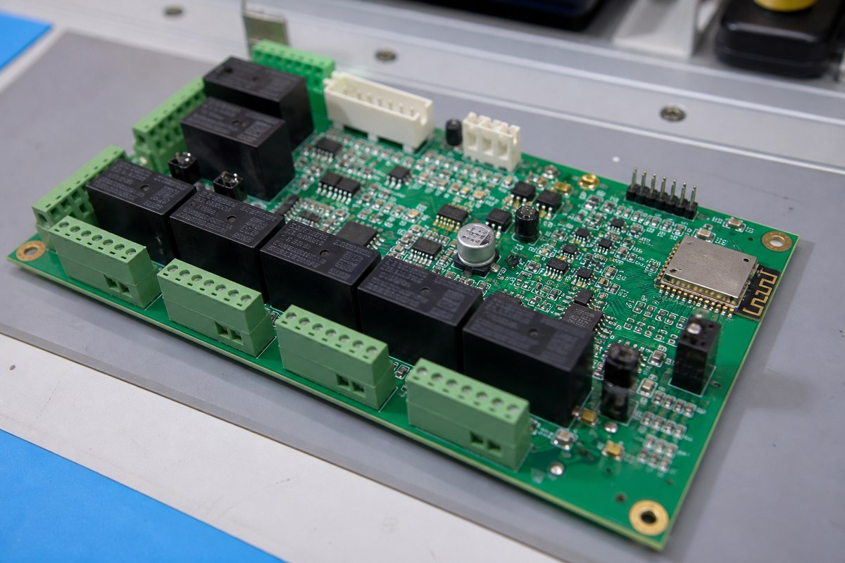
Car charger circuit board, manufacturing and assembly for an automotive USB charging module

What Is a Car Charger Circuit Board and How Does It Work?

A car charger PCB is a compact power-conversion assembly that turns the vehicle supply into the voltage and charging behavior required at one or more USB ports. Power normally enters through the module connector, passes through protection and filtering, reaches the switching converter, and then flows through the charging controller or port controller to the USB output.

  • Input protection: Limits damage from reverse connection, overvoltage, transient events or a short that the product specification requires the module to withstand.
  • DC-DC conversion: Regulates the varying vehicle input to the output needed by the selected charging architecture.
  • Charging control: Identifies or negotiates the permitted output behavior for USB-A, USB-C or USB Power Delivery.
  • Filtering and grounding: Contain switching noise and give the power and control circuits a stable reference.
  • Connector and enclosure path: Carry current to the cable, support insertion forces and help move heat away from the board.

These blocks work as one system. A capable controller cannot compensate for an undersized current path, and a large copper area will not solve a poor thermal connection beneath the power package. The design should therefore be reviewed from the vehicle input to the USB contact rather than as isolated components.

What Types of Car Charger PCBs Are Used for USB-A, USB-C and USB PD Modules?

The port type sets only part of the design; output behavior, available power, port count and mechanical format determine the actual circuit and assembly. Common USB car charger PCB variants include USB-A, USB-C, USB PD and multi-port boards. Two products can use the same connector while requiring different controllers, power stages, firmware and validation.

  • USB-A charging boards: Commonly combine a regulated power stage with a charging-port controller and a mechanically supported receptacle. The layout must protect output voltage from cable and connector losses, while the assembly drawing defines connector position, shell tabs and orientation.
  • USB-C charging boards: Add configuration and attachment-detection requirements. The smaller connector geometry and inaccessible joints may also change stencil design, inspection access and the method used to verify connector alignment.
  • USB PD charging boards: Require a compatible power stage, PD controller and approved configuration for the profiles the product is intended to provide. USB-IF maintains the current USB Power Delivery specification; hardware, controller configuration and functional testing should refer to the same approved product requirement.
  • Multi-port charging boards: Add power sharing, simultaneous-load behavior, denser connector placement and concentrated heat. Evaluate a dual-port board under the intended combined load rather than testing each port separately and assuming the same result.

What Electrical and Protection Requirements Affect a Car Charger Circuit Board?

The protection circuit must be selected from the customer’s defined input conditions and failure tests, not from a generic “automotive” label. Vehicle supply conditions vary by product and system. The RFQ should state the normal input range, abnormal-input conditions, transient requirements and recovery behavior that the finished module must meet.

  • Reverse-polarity protection: Confirm how the circuit blocks or tolerates an incorrect supply connection and whether the selected device creates a significant voltage or thermal penalty.
  • Overvoltage and transient protection: Coordinate the suppressor, switch and converter ratings so the first protection device does not merely pass excessive stress to the next part.
  • Overcurrent and short-circuit behavior: Define the trip, limiting and recovery response at both the input and the USB output where applicable.
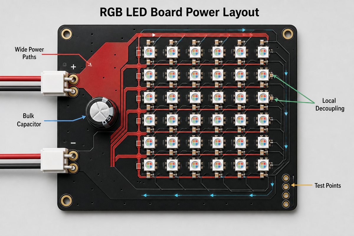
  • Input and output filtering: Place the filter around the actual noisy current path and verify it with the target wiring, load and enclosure conditions.
  • Connector-side protection: Review ESD and unintended voltage exposure at the user-accessible port as part of the product requirement.

The protection parts also influence placement and heat. For example, putting a suppressor close to the input connector can shorten its discharge path, but the surrounding copper, clearances and nearby heat-sensitive components still need to suit the specified stress. The right outcome is a coordinated protection path, not the maximum part rating in every position.
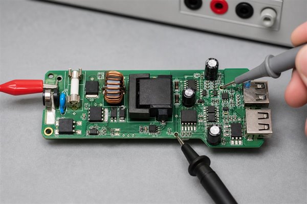
Car charger circuit board, input protection and power conversion section

How Should the Power Layout Be Designed for a Car Charger PCB?

A reliable layout keeps the high-current path wide and continuous while making the switching loop physically small. The two goals are related but not identical. Current capacity depends on the complete conductor path; switching behavior depends heavily on loop area, component placement and the return path.

  • Follow the power path: Review the route from input connector to protection device, converter, inductor, output capacitor and USB connector. Pad exits, thermal reliefs, via transitions and connector contacts can be more restrictive than the main trace.
  • Minimize the switching loop: Place the switching device, inductor and high-frequency capacitors according to the controller manufacturer’s layout guidance. Keep sensitive feedback and configuration signals away from noisy nodes.
  • Provide a deliberate return path: Avoid splitting the reference beneath critical control or high-frequency paths. Ground vias should support the intended current and thermal flow rather than being added without a clear function.
  • Avoid copper neck-downs: Check changes in width at pads, fuses, shunts, vias and connector pins. Local loss and heat often appear where the conductor becomes narrow for only a short distance.
  • Plan test access: Add stable measurement points for the input, regulated output, port output and key control nodes without disturbing the power loop.

During DFM, the layout should be checked against the finished copper, drill and assembly constraints that will actually be produced. A visually broad polygon is not proof of current capacity if its connection to a pad passes through a narrow spoke or an insufficient via group.

How Should Heat Be Managed in a Compact Car Charger PCB?

Thermal control starts by identifying where loss occurs and where that heat can leave the assembled module. The converter, MOSFETs, inductor, protection devices and connector contacts can all become limiting points. Their temperatures depend on conversion loss, conductor resistance, airflow, enclosure contact and how nearby heat sources interact.

  • Copper spreading: Connect useful copper to the thermal pad or power node without enlarging the noisy switching node unnecessarily.
  • Thermal vias: Move heat into useful copper on other layers; confirm drill size, finished hole condition and solder-control strategy with the manufacturer.
  • Stencil apertures: Segment exposed-pad openings when needed to balance solder coverage, voiding risk and package seating.
  • Component spacing: Keep electrolytic capacitors, plastics and other temperature-sensitive parts away from concentrated heat where the enclosure permits.
  • Loaded measurement: Test the assembled module at defined loads and ambient conditions, then record the hottest component and voltage drop along the main power path.

A bench result with the bare board exposed may not represent a closed dashboard or console enclosure. If the product depends on a housing contact or metal heat path, that interface belongs in the validation setup and the mechanical drawing.

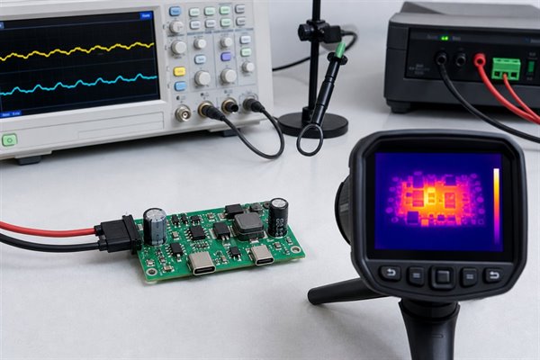
Car charger circuit board, thermal and electrical verification in a compact module

What PCB Materials, Copper Weight and Stackup Are Suitable for Car Charger PCBs?

FR-4 is a common starting material, but layer count, finished copper and board thickness should follow the electrical, thermal and mechanical needs of the specific module. There is no single construction that fits every car charger circuit board.

  • When two layers may fit: A two-layer board can be practical when the power is moderate, component density is low, the ground return remains continuous and enough copper area is available for current and heat spreading. Verify voltage drop, hot spots and switching behavior on the assembled module.
  • When four layers may help: Four layers become useful when the board needs a more continuous reference plane, denser routing, better separation of power and control paths, additional heat spreading or a smaller outline. Adding layers without assigning a function to them increases cost without guaranteeing better performance.
  • What the drawing should control: State the laminate or approved material requirement, final thickness, layer count, finished copper, surface finish and stackup. Copper weight alone is not a current guarantee because a narrow pad exit, via transition, solder joint or connector contact can still create local resistance and heat.
  • How to confirm the choice: Select the surface finish for the actual component, solderability, storage and customer requirements, then use fabricated-board and assembled-product results to verify that the selected construction meets the electrical, thermal and mechanical limits.

What DFM Checks Matter Before Car Charger PCB Manufacturing?

DFM should inspect the complete input-to-output path and its mechanical interfaces because current, thermal and connector failures often develop across more than one footprint. A useful review marks the exact feature, explains the possible failure and proposes a change that the customer can approve.

  • Current-path continuity: Trace the input connector to the protection stage, regulator, inductor, output capacitor and USB connector. Check every neck-down, via group, thermal relief and high-current pad.
  • Thermal-pad manufacturability: Review pad dimensions, via layout, solder-mask openings and stencil segmentation for power packages with exposed pads.
  • Connector fit: Compare the footprint, shell tabs, centerline, board edge and enclosure opening. Confirm that placement and inspection remain possible after panelization.
  • Assembly clearance: Check component spacing around the inductor, power devices and connectors for placement, soldering, rework and mechanical load.
  • Inspection and test access: Identify hidden joints and decide whether visual inspection, AOI, X-ray, a mechanical gauge or a powered test can detect the relevant defect.
  • File consistency: Cross-check Gerber or ODB++, drill data, BOM, centroid file, assembly drawing and mechanical model for revision, footprint and coordinate conflicts.

A focused car charger circuit board DFM review should distinguish a required correction from an optional cost or process suggestion. That distinction helps the buyer approve changes without turning every manufacturing preference into a product requirement.

How Is a Car Charger Circuit Board Manufactured and Assembled?

Manufacturing begins with the approved PCB construction and ends with an assembled, identified unit that can be tested against the intended charging behavior. The process route changes with the board design and component set, but the sequence should preserve product identity at every stage.

  • CAM and panel review: Confirm the approved stackup, copper features, drill data, solder mask, finish and panel method before tooling. This check catches file or clearance conflicts that could create a fabrication defect before production records are issued.
  • PCB fabrication: Build the layers, plated holes, solder mask and surface finish to the fabrication drawing. Bare-board electrical testing verifies the finished PCB for opens and shorts before assembly begins.
  • Solder-paste printing: Set stencil apertures from the approved component and footprint data. Inspect the print where fine-pitch controllers, exposed thermal pads or large power pads create bridging, insufficient-paste or voiding risks.
  • SMT placement: Place the power IC, MOSFETs, controller, inductor, capacitors and protection devices from the approved BOM with the correct orientation. Placement inspection catches a wrong, missing or shifted part before it creates a placement defect at reflow.
  • Reflow soldering: Use a profile suited to the approved solder paste, board mass and package set. Review joint formation and exposed-pad behavior because poor wetting, voiding or package lift can create electrical and thermal failures.
  • Connector and through-hole assembly: Install USB receptacles, input terminals and mechanically loaded parts according to the assembly drawing. Verify orientation, shell seating and solder joints to prevent a mechanical defect, retention failure or intermittent contact.
  • Inspection, programming and functional test: Apply the methods required by package and product failure risks, then record results against the correct PCB, BOM and program identity. Failed or mismatched units remain separated until reviewed and dispositioned.

The manufacturing record should make substitutions, rework and program changes visible. This is especially important when several variants share the same bare PCB but use different components or charging configurations.

How Are USB-C, USB PD and Power Components Controlled During Assembly?

Assembly control must prevent visually similar parts or boards from leaving production with the wrong charging function. The BOM, placement data, program file and test profile should use a shared variant identifier.

  • PD controller and configuration: Map each hardware revision to its approved configuration or firmware. Verify the loaded identity where programming is part of the build.
  • Power IC and MOSFETs: Check the exact manufacturer part number, package, orientation and thermal-pad condition. Approved alternatives require an electrical and thermal review, not just footprint compatibility.
  • Inductor and capacitors: Control electrical rating, package height, polarity where applicable and supplier-approved substitutions that can affect loss, heat or fit.
  • USB connector: Confirm connector orientation, shell seating, mechanical tabs and solder joints. Hidden joints need an inspection method suited to their geometry.
  • BOM revision: Keep consigned, turnkey and customer-approved components clearly separated so purchasing does not introduce an unreviewed alternative.

When one bare board supports several port or power variants, physical labeling and electronic identity should agree. Functional testing should then check the output behavior assigned to that variant rather than applying one generic test to every assembly.

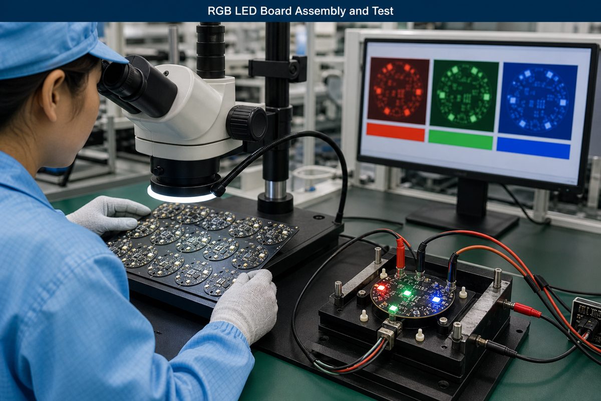
How Should Car Charger PCBAs Be Inspected and Functionally Tested?

Inspection and testing should be selected by failure mode and production stage. No single method proves solder quality, firmware identity, charging negotiation, output stability and thermal performance.

  • Before assembly: Bare-board electrical testing checks PCB opens and shorts.
  • During assembly: SPI may be used when paste volume or alignment is a significant process risk. AOI or visual inspection can detect applicable placement, polarity and visible-joint defects.
  • For hidden joints: X-ray may be applied to selected bottom-terminated packages, exposed pads or inaccessible connector joints when it can reveal the defined defect.
  • After programming: A readback or identity check confirms the expected controller configuration where the product requires it.
  • Powered testing: No-load and loaded output, port detection, requested PD profiles and simultaneous-load behavior can be checked against customer-defined limits.
  • Product validation: Temperature rise, transient response and EMI/EMC testing belong in the plan only when the applicable specification, setup and acceptance criteria are defined.

IPC J-STD-001J and IPC-A-610J address soldering process requirements and post-assembly acceptance, respectively. Purchase documents still need to name the applicable revision, class and customer-specific criteria. Functional testing complements those checks; it does not replace structural inspection.

Car charger circuit board, functional testing of an assembled PCBA before shipment

What Common Car Charger PCB Failures Should Be Checked Before Mass Production?

Failure analysis should begin with the symptom and a reproducible operating condition because the same visible fault can come from the PCB, component, program, connector or test setup. Replacing a component or adding copper before locating the cause can hide the original defect and create a new one.

  • Excessive temperature: Measure the converter, MOSFET, inductor, protection stage and connector under the intended load. Check whether loss comes from the component, copper path, solder joint or enclosure interface.
  • Voltage drop: Measure before and after pad exits, vias, protection devices and connector contacts. The weakest short segment can dominate the total loss.
  • Unstable charging or resets: Review input transients, loop layout, grounding, output capacitance, controller configuration and the test cable or load.
  • USB recognition failure: Compare the installed controller, configuration resistors, firmware or PD profile with the intended variant.
  • Connector solder cracking: Inspect shell tabs, mechanical support, board-edge position and enclosure loading rather than treating the joint as an electrical connection only.
  • Weak multi-port performance: Test simultaneous load, power sharing and thermal concentration with both ports active.
  • EMI-related instability: Review the high-frequency loop, filter placement, reference path and cable setup before changing the entire stackup.

A corrective action is ready for the next build only after the cause, affected units, design or process change and verification result are documented. If the same feature appears in another variant, the review should include that related board before volume release.

How Do You Move a Car Charger PCB From Prototype to Mass Production?

A prototype proves that the tested units can work; a pilot build proves that the intended files, materials, assembly route and test limits can produce repeatable units. The transfer does not need a long internal procedure, but it does need five items to remain aligned.

  • PCB data: Update and freeze the Gerber or ODB++ after approved PCB changes.
  • Component data: Freeze the BOM and record any approved substitutions.
  • Program identity: Match the firmware or controller configuration to the hardware revision.
  • Assembly definition: Carry the assembly drawing and connector datum used by the approved sample into the pilot package.
  • Test limits: Use the same functional-test conditions and pass limits that supported the production decision.

The pilot should reveal undocumented rework, difficult connector assembly, variable thermal-pad soldering, unstable tests or material substitutions before they become volume problems. Once corrected, those changes need to appear in the files used for the next order, not only on a reworked sample.

What Files Are Needed for a Car Charger PCB Manufacturing Quote?

A quote becomes more accurate when the supplier can identify the PCB construction, installed components, mechanical interfaces and required tests from one consistent package. These files control the quoted material, tooling, assembly and test scope because each car charger PCB manufacturer is pricing the same product definition. At minimum, provide five groups:

  • PCB data: Gerber or ODB++, drill files and fabrication drawing.
  • Assembly data: BOM, centroid or pick-and-place file and assembly drawing.
  • Electrical definition: Schematic, required USB functions and approved controller configuration or firmware where applicable.
  • Mechanical definition: Board outline, connector datum, mounting points, height limits and enclosure interface.
  • Commercial and test inputs: Prototype and volume quantities, sourcing responsibility, inspection requirements, powered-test conditions and expected records.

Open items can be listed instead of guessed. The supplier should return the assumptions that affect material, tooling, programming or test cost so quotations can be compared on the same scope.

Why Choose EBest Circuit for Car Charger PCB Manufacturing and Assembly?

EBest Circuit can combine PCB fabrication, component sourcing, SMT, through-hole and mixed assembly within one car charger PCBA project. The same project scope can keep the board construction, component identity, connector assembly and test requirements aligned from prototype through repeat production.

  • Car-charger-specific DFM: The free review can identify current-path neck-downs, exposed-pad and stencil risks, connector alignment issues, assembly clearances and missing test access.
  • PCB and PCBA coordination: Fabrication and assembly decisions can be reviewed against the same BOM, mechanical interface and variant definition.
  • Component sourcing control: Manufacturer part numbers, customer-supplied items and approved substitution boundaries can be agreed before purchasing.
  • Applicable inspection and testing: The proposed route can match visual inspection, SPI, AOI, X-ray, programming or functional testing to the actual package and product risks.
  • Quality-system evidence: EBest holds IATF 16949 and ISO 9001:2015 certifications, together with RoHS and UL credentials. Buyers can request current documents and verify the covered legal entity, site and service scope for the proposed order.

The customer benefit is a clearer transition from design review to an assembled and testable product, with fewer gaps between the PCB files, BOM, controller configuration and acceptance requirements. Send the current package to confirm which capabilities and records apply to your specific module.

FAQs About Car Charger Circuit Boards

Q1: Is a car charger circuit board the same as an EV charger PCB?

A1: No, they serve different power systems. The board discussed here powers USB devices from a low-voltage vehicle supply. An EV onboard or traction-battery charger operates at a different voltage and power level and requires a different isolation, safety, control and validation architecture.

Q2: Does a USB-C connector automatically mean the board supports USB PD?

A2: No, the connector alone does not provide PD. USB-C defines the connector and interface framework. USB Power Delivery support also depends on a compatible controller, power stage, configuration and functional test that verifies the profiles approved for the product.

Q3: Can one car charger PCB support USB-A and USB-C ports?

A3: Yes, when both ports are designed as one power system. The board must allocate the available power, use the required charging controllers, maintain connector clearances and handle the combined heat. Simultaneous-load testing should confirm that one active port does not cause the other to fall outside its approved output behavior.

Q4: Is a four-layer PCB always better for a car charger?

A4: No, layer count should solve a defined design need. Four layers can improve reference continuity, routing density and heat spreading, but a well-designed two-layer board may be suitable when current, space and EMI requirements allow it. Assign a purpose to each added layer before accepting the extra cost.

Q5: What usually causes a car charger PCB to overheat?

A5: Overheating usually comes from several losses adding together. Common contributors include converter loss, an undersized copper or via path, poor exposed-pad soldering, unsuitable inductor or MOSFET selection, connector resistance and an ineffective enclosure heat path. Loaded temperature measurements can identify which location limits the design.

Q6: Why can output voltage be correct with no load but low during charging?

A6: The load reveals resistance that a no-load check cannot show. Protection devices, copper neck-downs, vias, solder joints, connectors and cables can each contribute voltage drop. Measure before and after each segment under the intended load instead of increasing copper everywhere without locating the loss.

Q7: Does AOI prove that a car charger PCBA will charge correctly?

A7: No, AOI verifies only suitable visible features. It can detect applicable placement, polarity and solder-joint defects, but it cannot prove the controller configuration or charging response. Correct charging behavior requires the intended components and program plus a powered functional test with defined limits.

Q8: When is X-ray inspection useful?

A8: Use X-ray when the critical joint cannot be seen directly. It can help evaluate selected bottom-terminated power packages, exposed pads or inaccessible connector joints. The drawing or inspection plan should name the package, defect of concern and acceptance basis rather than requiring X-ray for every component.

Q9: Can different car charger variants share one bare PCB?

A9: Yes, if variant identity is maintained beyond the bare board. The BOM, installed components, controller configuration, product label and test profile must remain linked. A common PCB saves tooling only when production can prevent one assembled variant from being tested or shipped as another.

Q10: What should be tested on the first assembled samples?

A10: Test the features most likely to change between design files and the assembled product. Confirm mechanical fit, connector position, installed variant, programmed identity where applicable, output behavior under the intended load, voltage drop and the main thermal hot spots. Record any rework before the pilot build.

Conclusion

EBest provides car charger PCB manufacturing and car charger PCB assembly support from DFM and component sourcing through PCB fabrication, SMT or mixed assembly, applicable inspection and functional testing. The route is selected around the actual USB interface, power path, connector, thermal design and product acceptance requirements.

Send the Gerber or ODB++, BOM, required quantity and test requirements to sales@bestpcbs.com. EBest can review the files, identify manufacturing risks and prepare a quotation for the defined PCB and PCBA scope.

You may also like

Fiber Optic FPV Drones PCB Design and Manufacturing Guide

August 24th, 2026

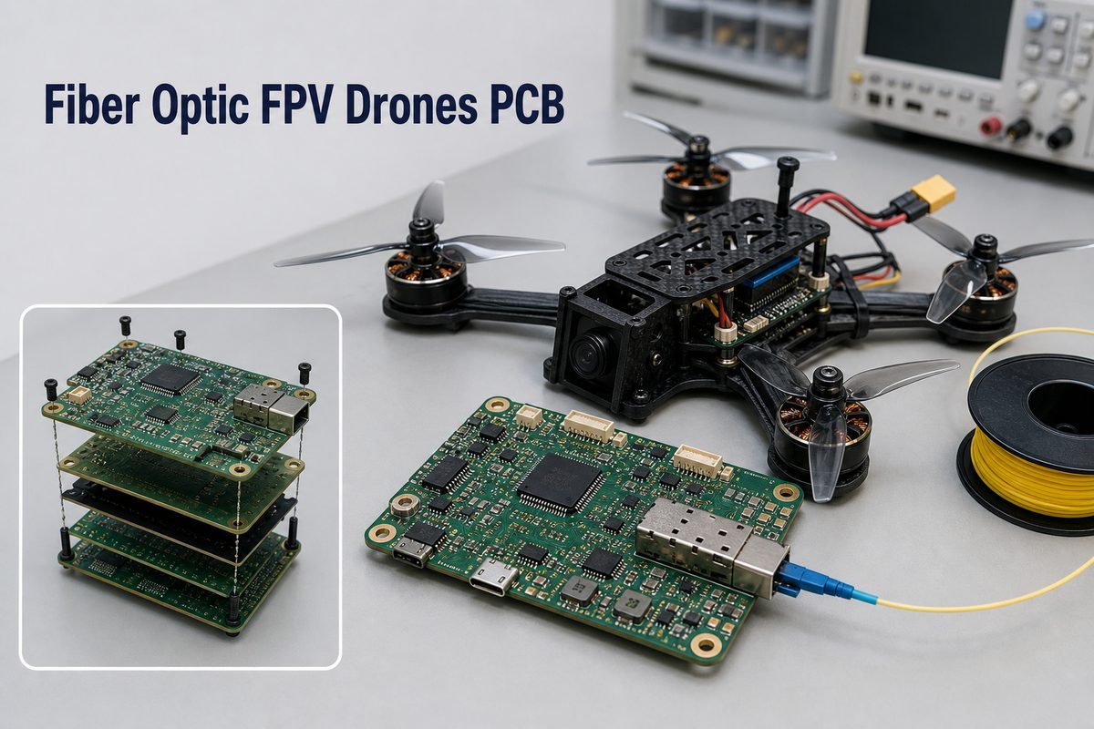
A fiber optic fpv drones PCB connects the flight controller, camera or video processor, optical transceiver, power regulation, sensors, and motor-control interfaces in a compact airborne electronics system. The fiber carries optical data, but the PCB still has to manage high-speed electrical signals, switching noise, heat, vibration, connector stress, and strict weight limits.

The design should therefore be treated as a coordinated set of signal, power, mechanical, and manufacturing decisions. This guide focuses on the PCB and PCBA engineering needed for lawful industrial, inspection, research, and communications applications. Exact data rates, environmental limits, interfaces, and acceptance tests must be defined for each project.

Fiber Optic FPV Drones PCB with optical transceiver, flight controller, and fiber interface

What Is a Fiber Optic FPV Drones PCB?

A fiber optic FPV drones PCB is the board-level platform that routes control and video data between the drone electronics and an optical communication module. It may be one integrated assembly or several boards connected as a flight-control stack, camera board, optical-interface board, power board, and electronic speed controller system.

The optical fiber does not carry electrical power to the aircraft. A battery and local regulators still power the processor, sensors, camera, transceiver, and other loads. The PCB must keep those rails stable while motors and switching converters create rapid current changes. It must also preserve the electrical channel between the processor or video interface and the optical transceiver.

How Does a Fiber Optic FPV Drone Work?

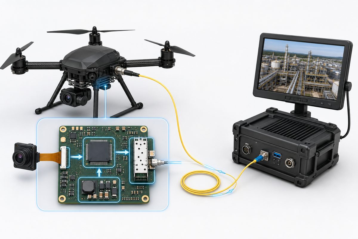
A fiber-linked FPV platform converts electrical control and video data into optical signals, sends them through a lightweight fiber, and converts them back at the opposite end. The exact phrase fiber optic fpv drone how it works often leads readers to the link itself, but reliable operation also depends on the electronics around that link.

  1. The camera and sensors create video and flight data.
  2. The flight controller processes commands and sensor inputs.
  3. An electrical interface passes selected data to an optical transceiver or conversion module.
  4. The transceiver converts electrical data to light for transmission through the fiber.
  5. The ground-side unit performs the reverse conversion for the display and controller.

This arrangement can remove the primary control/video path from a conventional radio link, but it does not make the complete aircraft immune to every disturbance or failure. Power noise, damaged connectors, excessive fiber bending, processor faults, sensor errors, and mechanical stress can still interrupt the system.

Fiber optic FPV system architecture showing the drone PCB, optical link, and ground unit

Which Circuit Boards and Functional Blocks Make Up the System?

The system normally combines flight control, video, optical communication, power conversion, sensing, and motor interfaces. These functions can share one board, but separating them may simplify noise control, thermal management, service, and mechanical placement.

Board or Block Main Function PCB Design Focus
Flight controller Processes sensor data and generates control outputs Clean sensor power, stable clocks, short return paths, vibration-aware placement
Optical interface Converts electrical data to and from optical signals Differential routing, decoupling, connector retention, transceiver heat
Camera or video board Captures and conditions the FPV image stream High-speed interface integrity, low-noise power, compact interconnects
Power distribution and regulation Feeds logic, camera, optical module, and peripheral rails Current capacity, filtering, protection, thermal paths
ESC or motor interface Drives or commands the motors High-current loops, switching noise, MOSFET cooling, isolation from sensors

For a broader system comparison, our guide to the types of circuit boards used in drones explains how flight-control, power, camera, sensor, and communication boards divide the work.

What Makes an FPV Drone PCB Board Different?

An fpv drone pcb board must operate under tighter weight, space, vibration, and power-noise constraints than many stationary electronics. In a fiber-linked design, the optical interface adds another high-speed data path and a mechanically sensitive connection near a moving platform.

  • Mixed electrical environments: quiet sensors and high-speed data operate near motor switching and battery current.
  • Mass and balance: board dimensions, copper weight, connectors, shields, and the fiber assembly affect mechanical integration.
  • Limited cooling: airflow changes with enclosure, speed, board orientation, and nearby components.
  • Continuous movement: vibration can fatigue solder joints, connectors, cables, and unsupported components.
  • Service constraints: densely stacked boards need accessible test points and a clear replacement strategy.

These constraints should be set before schematic capture. Adding the optical module late can create blocked airflow, long data routes, poor connector access, or an unstable center of mass.

How Should an FPV Drone Controller PCB Handle the Optical Interface?

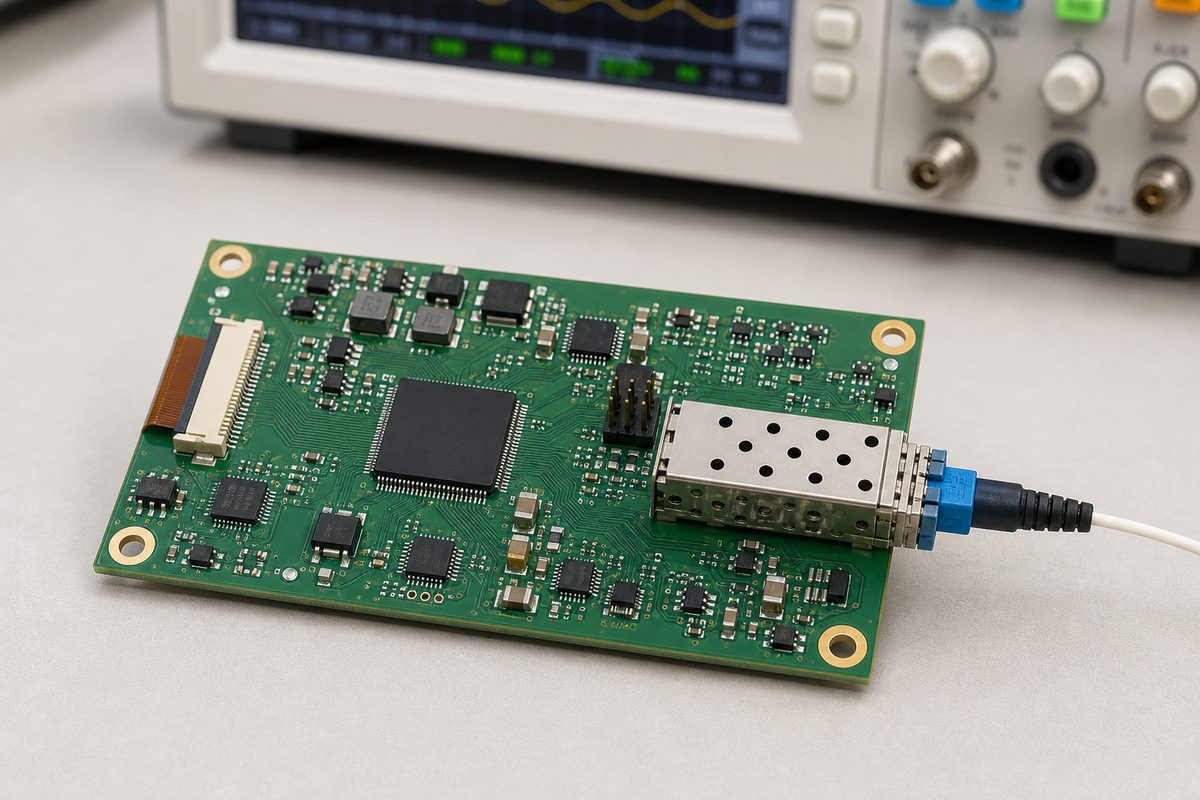
An fpv drone controller pcb should treat the optical transceiver as a high-speed electrical load with its own power, thermal, signal, and connector requirements. The fiber begins at the optical port; everything between the processor and that port is still an electrical PCB channel.

Start with the selected module datasheet and define its host interface, supply rails, peak current, reset behavior, clocking, connector, and thermal limits. Keep high-speed pairs short, maintain a continuous reference plane, and avoid stubs or unnecessary test pads. Place local decoupling close to supply pins and provide a low-inductance return path.

Connector orientation must be coordinated with the enclosure and fiber path. The optical connector or pigtail should not transfer repeated pull or twist directly into small solder joints. If the design uses a separate optical daughterboard, specify the board-to-board connector, retention method, mating cycle, and service access before layout.

Close view of an FPV drone optical interface PCB with transceiver and controlled routing

How Should Power Domains Be Separated from Motor Noise?

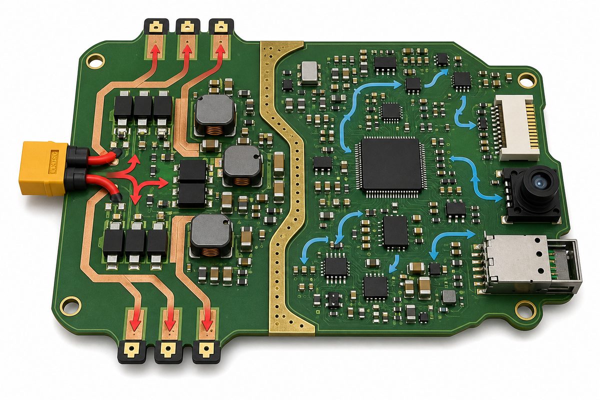
Power-domain planning should prevent motor and converter noise from disturbing the flight controller, camera, sensors, or optical interface. A single battery may feed every function, but that does not mean all loads should share the same unfiltered path.

  • Keep high-current battery and motor loops physically compact.
  • Separate sensitive regulators from switching nodes and hot power components.
  • Use the regulator vendor’s recommended input, output, and compensation layout.
  • Place high-frequency decoupling at the IC pins and bulk capacitance near load groups.
  • Do not split a reference plane beneath a high-speed signal simply to create visual separation.
  • Plan current return paths before routing signals between functional zones.

Power integrity should be checked during load transitions, not only at idle. The optical transceiver, processor, and camera may react differently to voltage droop or ripple. Test limits should come from the component datasheets and system specification rather than one generic ripple target.

Drone PCB power-domain layout separating motor current from flight-control and optical circuits

How Should High-Speed Video and Control Data Be Routed?

High-speed routes should be designed as transmission lines whose geometry, return path, vias, and connector launches are controlled from the processor to the optical module. The required impedance and matching tolerance depend on the actual electrical interface and component datasheets.

Practical layout checks include:

  • Define the stackup and target impedance with the PCB fabricator before final routing.
  • Keep differential-pair geometry consistent and avoid abrupt neck-downs.
  • Minimize stubs, layer changes, and unnecessary connector transitions.
  • Add nearby return vias when a high-speed pair changes reference layers.
  • Separate fast data from switching nodes, motor phases, and noisy clock sources.
  • Reserve test access that does not create an unacceptable discontinuity.

Our high-speed digital PCB design guide covers stackup, return paths, differential routing, vias, crosstalk, and power integrity in more detail. When waveform margin matters, an eye diagram can be combined with TDR, channel measurements, and functional testing under defined conditions.

What Does the Fiber Optic FPV Drone Cable Change Mechanically?

The fiber optic fpv drone cable adds bend-radius, strain-relief, routing, connector, and spool-integration requirements that must be resolved with the PCB and enclosure. The board should not become the mechanical anchor for an unsupported fiber path.

Define the minimum bend radius, connector or pigtail geometry, retention method, exit angle, and allowable movement from the chosen fiber and module documentation. Keep the path away from sharp board edges, propulsive components, hot surfaces, and service fasteners. If a separate spool or dispensing assembly is used, its loads should be carried by the mechanical structure rather than small PCB pads.

Mechanical review should also cover assembly sequence. A connector that is electrically correct may be unusable if it cannot be mated after the boards are stacked. A short flexible interconnect or daughterboard may improve serviceability, but it adds connectors and possible signal discontinuities that require validation.

Which PCB Stackup and Materials Fit the Design?

The stackup should be chosen from routing density, electrical interface speed, power-current needs, board thickness, weight, and manufacturing tolerance. There is no universal layer count or laminate for every fiber-linked drone controller.

Design Need Possible PCB Direction Decision Check
Compact controller with moderate routing density Multilayer FR-4 Reference planes, finished thickness, thermal margin, impedance feasibility
Fine-pitch processor or dense camera interface HDI construction when justified Escape routing, microvia structure, assembly yield, cost
Moving camera or constrained interconnect Flexible or rigid-flex circuit Bend zone, stiffener, dynamic-cycle requirement, connector reduction
Higher-current power section Localized heavier copper or separate power board Temperature rise, etching limits, weight, copper balance

Controlled impedance requires agreement on dielectric thickness, copper thickness, trace geometry, and material properties. Our impedance control PCB guide explains how design targets connect to fabrication and test coupons.

How Should Vibration, Heat, and Environmental Exposure Be Managed?

Reliability starts with the actual mounting, airflow, duty cycle, temperature, humidity, and vibration profile. A coating or stronger material cannot compensate for unsupported connectors, poor thermal paths, or components placed in high-strain areas.

  • Keep heavy components away from unsupported board edges where possible.
  • Use mounting-hole and keep-out geometry that avoids local copper or laminate stress.
  • Review connector retention and cable strain relief as part of the enclosure.
  • Provide copper area and thermal vias for regulators, processors, and power devices when the package guidance requires them.
  • Measure component temperatures in the real enclosure and operating airflow.
  • Select conformal coating or sealing only after checking connectors, sensors, optical surfaces, rework, and service requirements.

Board cleanliness matters if a coating will be applied. Flux residue or moisture trapped beneath a coating can create reliability problems instead of preventing them.

Which DFM and PCBA Checks Matter Before Production?

DFM and PCBA review should connect the schematic, layout, component data, mechanical model, and test plan before the first build. The review is most useful when it identifies risks that can still be changed.

  • Fabrication data: final Gerber or ODB++ data, drill files, stackup, controlled-impedance table, and board outline.
  • Assembly data: BOM with manufacturer part numbers, centroid file, polarity notes, approved substitutes, and special handling instructions.
  • Mechanical data: enclosure model, connector height, board stack spacing, mounting hardware, and fiber exit path.
  • Process checks: fine-pitch escape, solder-mask clearances, thermal-pad design, panelization, fiducials, and test-point access.
  • Supply checks: component lifecycle, optical-module availability, connector lead time, and traceable alternates.

If the design includes a dense image path, our camera PCB module guide provides related manufacturing and assembly considerations.

How Should the PCB Be Tested and Validated?

Validation should move from bare-board checks to assembled-board inspection and then to system testing under defined electrical and mechanical conditions. A board that powers on once has not yet demonstrated stable optical, control, sensor, and power performance.

Test Stage What It Checks Typical Evidence
Bare PCB Continuity, isolation, dimensions, holes, and controlled impedance when specified Electrical test record, dimensional inspection, impedance report or coupon data
PCBA inspection Placement, polarity, solder joints, bridges, voiding, and hidden connections AOI, X-ray where appropriate, visual inspection, reflow records
Power-up Rail sequence, current draw, ripple, reset, clocks, and thermal behavior Measured waveforms, current log, thermal measurements
Interface validation Camera, controller, sensor, and optical data paths Functional logs, error counters, waveform or channel measurements
System validation Operation in the intended enclosure, wiring, motion, and environment Approved test procedure and pass/fail report
Inspection and electrical testing of a fiber optic drone PCBA

FAQ About Fiber Optic FPV Drones PCB

  • Does the optical fiber replace every communication circuit?
    No. It can carry selected control and video data, but the system still needs processors, interfaces, sensors, local power, and possibly other links. The exact architecture depends on the product specification.
  • Does the PCB route optical signals as copper traces?
    No. Copper traces carry electrical signals to the optical transceiver. The transceiver converts those signals to light, which then travels through the fiber.
  • Is a high-frequency laminate always required?
    No. Material choice depends on the electrical interface, route length, loss budget, stackup, temperature, and fabrication tolerance. Multilayer FR-4 may be suitable for some designs, while others need a lower-loss construction.
  • Can the optical module share a regulator with the flight controller?
    Only if the load transients, ripple, sequencing, noise, and thermal limits remain within every component’s requirements. Separate filtering or regulation may be safer, but the decision should be verified by measurement.
  • What files are needed for PCB manufacturing and assembly review?
    Prepare fabrication data, drill files, stackup, impedance requirements, BOM, centroid file, assembly drawing, mechanical data, optical-module documentation, quantities, and the intended test plan.

How Can EBest Circuit Support Your Drone PCB Project?

A dependable fiber optic fpv drones PCB project needs the optical interface, flight-control electronics, power architecture, mechanics, and manufacturing data to agree before production. At EBest Circuit, we support PCB design review, PCB fabrication, component sourcing, PCBA assembly, impedance-related build requirements, and inspection for custom electronics projects.

Send your Gerber or ODB++ data, stackup, impedance table, BOM, centroid file, board dimensions, optical-module datasheet, quantities, mechanical constraints, and test requirements to sales@bestpcbs.com. We can review the manufacturing package and help prepare the board for prototype or production quotation.

You may also like

Electronic Control Unit Board: From Design to Production

August 21st, 2026

An Electronic Control Unit board is the PCB or PCBA inside an automotive controller. It receives sensor data, runs control software, communicates with other vehicle modules, and drives loads such as motors, valves, relays, and solenoids. Unlike a general controller, an ECU board must remain stable under voltage transients, heat, vibration, moisture, and electromagnetic interference.

EBest Circuit supports ECU PCB design, fabrication, and assembly from engineering review and prototyping to volume production. For a project review, send the Gerber files, BOM, pick-and-place data, drawings, test requirements, quantity, and applicable automotive specifications to sales@bestpcbs.com.

Electronic Control Unit board installed in an automotive ECU enclosure

What Is an Electronic Control Unit Board?

An Electronic Control Unit board provides the electrical foundation of a vehicle control module. The bare PCB contains copper circuits, vias, component pads, and power and ground planes. After assembly, it becomes a PCBA containing processors, memory, communication interfaces, sensor inputs, protection devices, and output drivers.

Several related terms are often confused:

  • ECU: The complete control unit, including the PCBA, software, enclosure, connector, and thermal or sealing components.
  • ECM: An engine control module, which is one type of ECU.
  • ECU board: The bare PCB or assembled PCBA inside the unit.
  • Controller PCB: A broader category covering automotive and non-automotive control boards.

This distinction affects quotation scope. PCB fabrication, component sourcing, assembly, programming, coating, testing, and enclosure integration are separate deliverables unless the quotation states otherwise.

How Does an ECU Board Work?

An ECU board converts vehicle inputs into controlled outputs through several functional stages:

  • The power-input circuit filters the vehicle supply and protects the board from reverse polarity, overvoltage, ESD, and electrical transients.
  • Sensor-interface circuits condition signals from pressure, temperature, position, speed, current, and other sensors.
  • A microcontroller, processor, or system-on-chip compares the input data with programmed control logic.
  • Output drivers operate motors, injectors, pumps, valves, relays, lamps, or solenoids.
  • CAN, LIN, FlexRay, or Automotive Ethernet transceivers exchange data with other vehicle modules.
  • Diagnostic and watchdog circuits detect abnormal conditions and help the system enter a defined safe state.

The balance between these functions depends on the application. A body controller may contain many low- and medium-current outputs, while an ADAS controller places greater emphasis on processing speed, memory bandwidth, controlled impedance, and heat dissipation.

What Components Are Used on an Electronic Control Unit Board?

Most ECU boards contain the same functional blocks, although component count and performance vary.

Main functional components inside an automotive ECU board

Functional block Typical components Main concern
Power input TVS diode, filter, reverse-polarity protection Transients and voltage drop
Power conversion DC-DC converter, LDO, PMIC, inductors Efficiency, ripple, and heat
Processing MCU, MPU, SoC, FPGA Performance, safety, and lifecycle
Memory Flash, EEPROM, RAM Retention and programming
Sensor interface ADC, op-amp, filters, protection arrays Accuracy and noise
Communication CAN, LIN, FlexRay, Ethernet transceivers EMC and signal integrity
Output stage MOSFETs, relays, gate drivers, smart switches Current and junction temperature
Safety monitoring Watchdog and voltage supervisor Fault detection
Timing Crystal, oscillator, clock generator Stability and layout sensitivity

AEC-Q100, AEC-Q101, and AEC-Q200 may apply to ICs, discrete semiconductors, and passive components. These qualifications cover individual components rather than the complete ECU board, so PCB construction and assembly reliability still require separate controls.

Component selection should also consider operating temperature, package reliability, traceability, lifecycle, and approved alternatives. An electrically suitable component can still create production risk if it has limited availability or an unsuitable package.

Which Types of ECU Boards Are Used in Vehicles?

Different vehicle functions place different demands on the PCB.

  • Engine and transmission controllers: Accurate sensor measurement, fast processing, transient protection, and high-current outputs.
  • Body control modules: Multiple connectors and load drivers for lighting, doors, windows, seats, and comfort functions.
  • Chassis controllers: Fault detection and safety-related control for braking, steering, and suspension.
  • ADAS controllers: HDI routing, high-speed memory, controlled impedance, dense processors, and advanced cooling.
  • Battery management systems: Precise voltage measurement, isolation, creepage, clearance, and communication reliability.
  • Gateways and telematics units: Multiple vehicle networks, high-speed interfaces, security devices, and sometimes RF circuits.
  • Motor and inverter controllers: Strong immunity to high-current switching noise and high dv/dt environments.

An interior comfort controller does not need the same laminate, coating, thermal design, or validation plan as an engine-bay or battery-system controller. The mounting location, electrical load, and consequence of failure should guide the specification.

Which PCB Materials and Stackups Suit ECU Boards?

High-Tg FR-4 is commonly used because it supports multilayer construction and established automotive manufacturing processes. However, Tg alone does not determine suitability. The material review should also cover z-axis expansion, CAF resistance, moisture performance, copper adhesion, thermal decomposition, and compatibility with repeated assembly cycles.

Automotive ECU PCB materials and multilayer stackup cross-section

Requirement Suitable PCB construction
Standard body-control functions Multilayer high-Tg FR-4
Fine-pitch processors and memory HDI with microvias
High-current outputs Heavy copper or copper inlay
Automotive Ethernet Controlled-impedance multilayer PCB
RF or radar circuits High-frequency or hybrid laminate
Concentrated power-device heat Thermal vias, copper coins, or enclosure conduction

The approved stackup should define:

  • laminate grade;
  • core and prepreg thicknesses;
  • copper weight on each layer;
  • signal and reference-plane relationships;
  • controlled-impedance requirements;
  • via types and lamination cycles;
  • finished board thickness and tolerance.

Leaving these decisions open until production can change impedance, thermal performance, mechanical stability, and manufacturing yield.

How Should Power and Ground Be Designed on an ECU Board?

The power input must be designed for the vehicle supply rather than a stable bench source. Applicable transient conditions depend on the vehicle platform, voltage architecture, wiring harness, mounting location, and customer specification. Reverse polarity, cranking, overvoltage, and inductive-load disturbances should be translated into clear protection requirements before the schematic is released.

Automotive ECU PCB power input, grounding and high-current output layout

A typical power architecture includes:

  • input-current and reverse-polarity protection;
  • transient suppression and conducted-noise filtering;
  • regulated power rails and local decoupling;
  • controlled reset and power sequencing;
  • undervoltage and overvoltage monitoring;
  • clamping or freewheeling paths for inductive loads.

High-current returns should not share narrow copper paths with sensor grounds. However, splitting ground planes without analysing return currents can also increase noise and EMI. Power, digital, analogue, chassis, and load-return regions should therefore be connected through deliberate, low-impedance paths.

Copper sizing must account for current, pulse duration, voltage drop, temperature rise, vias, connectors, shunts, and neck-down areas. Widening one section of a trace does not solve a bottleneck elsewhere in the current path.

How Should Signal Integrity and EMC Be Controlled?

An ECU operates near motors, relays, switching converters, ignition circuits, wireless transmitters, and long wiring harnesses. EMC control must therefore begin at the connector and continue through placement, filtering, routing, grounding, shielding, and enclosure design.

Practical layout controls include:

  • place transient protection and filters close to external connectors;
  • route high-speed signals over continuous reference planes;
  • keep switching nodes compact and away from sensor and clock circuits;
  • control the geometry and return path of differential pairs;
  • minimise gate-drive and power-conversion loop areas;
  • place decoupling capacitors close to the relevant power pins;
  • avoid unnecessary stubs on communication buses;
  • provide test points for debugging and pre-compliance measurements.

CAN, LIN, and Automotive Ethernet have different termination, bandwidth, topology, and impedance requirements. They should not be treated as interchangeable two-wire connections.

Emission and immunity limits should be defined in the customer’s validation plan before the PCB layout is finalised. This allows the designer to reserve suitable filtering, shielding, grounding, component spacing, and test access instead of correcting EMC problems after the prototype has been assembled.

How Should Heat Be Managed on an ECU Board?

Thermal design should begin with the real power loss of regulators, processors, MOSFETs, smart switches, shunts, and relays. Average board temperature is not sufficient; each component must remain within its allowable junction temperature under the expected load and ambient conditions.

Common heat-control methods include:

  • wider copper areas around power devices;
  • thermal vias connected to useful internal or opposite-side copper;
  • heavier copper or copper inlays for high-current circuits;
  • exposed-pad packages with controlled solder-paste coverage;
  • thermal interface material between the PCBA and enclosure;
  • component spacing that avoids local hot spots.

Thermal vias provide limited benefit if they connect only to a small isolated copper area. Open vias beneath exposed pads may also draw solder away from the joint. Filled, capped, tented, or offset vias may be preferable depending on the package and assembly process.

Simulation should be followed by measurements on a representative assembly. Thermocouples, infrared imaging, and full-load operating tests help verify the complete heat path through the PCB, interface material, enclosure, and mounting structure.

How Is an Electronic Control Unit Board Manufactured?

An automotive PCB manufacturer should begin with a DFM review covering the stackup, copper balance, drill structure, impedance, panel design, assembly clearances, and test access. Conflicts between the Gerber files, BOM, drawings, and pick-and-place data should be resolved before materials are released.

Automotive ECU PCB assembly on an SMT production line

The main production stages are:

  • bare PCB fabrication and electrical testing;
  • solder-paste printing and SPI;
  • SMT placement and reflow;
  • AOI and X-ray inspection;
  • through-hole or selective soldering;
  • programming and serialisation;
  • ICT, boundary scan, or functional testing;
  • cleaning, conformal coating, or potting;
  • enclosure assembly and final inspection.

Large connectors, relays, transformers, and high-current terminals often require through-hole assembly. BGAs, QFNs, and bottom-terminated power packages generally require X-ray inspection because their solder joints cannot be fully evaluated by AOI.

If conformal coating is specified, the drawing should identify coating type, thickness, coverage, curing method, and keep-out areas. Connectors, programming contacts, grounding features, pressure ports, and selected test points may need to remain uncoated.

Which Tests and Standards Apply to ECU Boards?

No single standard covers the complete ECU board. The applicable combination depends on the vehicle manufacturer, mounting location, safety classification, electrical architecture, and product specification.

For a production-level overview, see our PCB assembly testing services guide.

Standard or control Application
ISO 26262 Functional safety of automotive electrical and electronic systems
ISO 16750 Electrical, mechanical, climatic, and chemical conditions
CISPR 25 Vehicle-component electromagnetic emissions
ISO 11452 Electromagnetic immunity
IPC-6012 Qualification and performance of rigid PCBs
IPC-A-600 Bare-board acceptability
IPC-A-610 Electronic assembly acceptability
IATF 16949 Automotive quality-management processes
AEC-Q100/101/200 Qualification of electronic components
PPAP Production-process and part approval

These documents serve different purposes. ISO 26262 addresses functional safety, while ISO 16750, CISPR 25, and ISO 11452 guide environmental and EMC validation. IPC standards cover PCB and assembly requirements. IATF 16949 applies to the manufacturing quality system, and AEC-Q specifications apply to individual components.

The customer should identify the applicable revisions, test severity, acceptance class, documentation requirements, and any OEM-specific additions before quotation. Without that information, two suppliers may quote very different inspection and validation scopes.

Automotive ECU board functional, thermal and CAN diagnostic validation

What Causes Electronic Control Unit Board Failures?

ECU failures often involve interactions between electrical stress, temperature, vibration, moisture, layout, materials, and manufacturing variation.

Failure symptom Possible cause Investigation or prevention
Intermittent reset Supply drop, ground bounce, cracked joint Review power integrity and solder joints
Communication loss Termination error, connector damage, EMI Test the bus, harness, and transceiver
Burned output stage Overcurrent, transient, inadequate cooling Check the load, clamping, copper, and heat path
Sensor drift Contamination, noise, unstable reference Inspect cleanliness, filtering, and grounding
BGA or QFN open Warpage, voiding, fatigue, board flex Use X-ray, cross-sectioning, or dye-and-pry
Internal PCB short CAF, moisture, contamination Review material, spacing, cleanliness, and humidity
Corrosion Residues, coating gaps, water ingress Improve cleaning, sealing, and coating control

Failure analysis should begin with operating history, fault codes, environmental exposure, and production-lot information. Electrical measurements can then be combined with X-ray, microscopy, cross-sectioning, thermal imaging, or material analysis.

Replacing the visibly damaged component may restore one board, but it does not prove that the underlying design, load, enclosure, or manufacturing issue has been corrected.

What Drives Electronic Control Unit Board Cost?

Cost is influenced by the complete manufacturing and validation package rather than PCB dimensions alone.

The main cost drivers are:

  • layer count and panel utilisation;
  • high-Tg, low-loss, CAF-resistant, or specialised laminates;
  • HDI, microvias, via filling, and sequential lamination;
  • controlled impedance and tighter tolerances;
  • heavy copper, copper inlays, and thermal structures;
  • automotive-qualified components;
  • X-ray, ICT, functional testing, and programming;
  • conformal coating, potting, and enclosure assembly;
  • PPAP documents and customer-specific reports;
  • prototype quantity and component availability.

Useful cost reductions include removing unnecessary HDI structures, improving panel utilisation, standardising material thicknesses, adding practical test access, and approving suitable component alternatives before shortages occur.

The lowest prototype price is not always the lowest production cost. Material substitutions, incomplete testing, poor component traceability, and repeated engineering changes can cost more than the initial saving.

What Should Buyers Check Before Ordering an ECU Board?

First confirm whether the quotation covers a bare PCB, assembled PCBA, programmed controller, or complete boxed unit. The scope should identify included materials, components, testing, documentation, fixtures, and engineering charges.

A complete quotation package should include:

  • Gerber or ODB++ data and drill files;
  • approved stackup and impedance requirements;
  • fabrication and assembly drawings;
  • BOM with manufacturer part numbers;
  • approved component alternatives;
  • pick-and-place data;
  • firmware and programming instructions;
  • test limits and expected outputs;
  • coating, potting, housing, and labelling requirements;
  • prototype and production quantities;
  • required standards, reports, and traceability.

Buyers should also review the supplier’s fabrication capability, SMT and through-hole processes, component controls, engineering response, inspection methods, change management, and automotive quality system.

IATF 16949 certification is relevant, but it should not be the only supplier-selection criterion. Confirm that the certification scope, production location, subcontracted processes, inspection equipment, and documentation system match the actual ECU project.

FAQs About Electronic Control Unit Boards

What does an Electronic Control Unit board do?

An ECU board receives sensor and network data, processes it through a microcontroller or processor, and controls vehicle loads. It also manages power conversion, communication, fault monitoring, diagnostics, and protection against electrical disturbances.

How many layers does an ECU PCB need?

There is no universal layer count. A simple controller may use four or six layers, while an ADAS, gateway, or processor-dense ECU may require additional layers or HDI. The decision should follow routing density, reference-plane needs, power distribution, EMC, and thermal requirements.

What PCB material is commonly used for ECU boards?

High-Tg FR-4 is widely used, but the exact grade depends on temperature, thermal cycling, humidity, CAF resistance, copper structure, and assembly conditions. Heavy-copper, HDI, low-loss, or hybrid constructions should be selected only when the project requirements justify them.

How are ECU boards tested after assembly?

Testing may include SPI, AOI, X-ray, programming verification, ICT, boundary scan, and functional testing. Automotive validation can add thermal cycling, vibration, humidity, electrical-transient, and EMC tests. The customer specification should define the conditions and pass limits.

What information is needed for an ECU board quotation?

For a bare PCB, provide fabrication data, stackup, drawings, material requirements, copper weights, impedance targets, quantities, and acceptance criteria. For PCBA, also provide the BOM, placement data, assembly drawings, programming files, test requirements, and coating or enclosure instructions.

An Electronic Control Unit board must combine protected power inputs, stable signal processing, reliable communication, thermal control, EMC performance, and traceable production. Material and process choices should follow the mounting environment, electrical loads, safety requirements, and validation plan rather than a generic automotive specification.

If you are looking for reliable OEM manufacturing, ODM production, prototype development, volume production, or a custom engineering solution, contact the EBest Circuit engineering team at sales@bestpcbs.com for technical support and a quotation.

You may also like

4 Layer Array Antenna PCB: Stackup, RF Layout and Manufacturing

August 19th, 2026

A 4 layer array antenna PCB combines antenna elements, controlled RF paths, reference planes and support circuitry in one board. Its measured performance depends on the manufactured stackup as much as the simulated antenna geometry.

Here, “4 layer” means four copper layers. It does not describe a four-element or 4 × 4 array. The final construction must match the operating frequency, antenna architecture and validation plan.

EBest Circuit provides multilayer RF and high-frequency PCB fabrication, impedance-control support, prototypes, small-volume production and PCB assembly. Send us your stackup, material requirements, impedance table, quantity and production data for review and quotation.

3D cutaway of a 4 layer array antenna PCB with antenna patches and four visible copper layers

What Is a 4 Layer Array Antenna PCB?

A four-layer array antenna PCB is an RF board with several coordinated radiating elements and a shared feed or beamforming network. The copper layers divide antenna, reference, power, control and component-routing functions.

A passive array may use a fixed feed network. A phased array antenna PCB also controls channel phase and often amplitude. PCB layer count and antenna element count are separate design decisions.

Term Meaning
4 layer PCB Four copper layers separated by dielectric materials
Array antenna PCB Multiple elements operating as one coordinated aperture
Phased array antenna PCB An array with controlled channel phase and usually amplitude

What Is a Phased Array Antenna, and How Does It Work?

A phased array antenna forms and steers a beam by controlling the relative phase of its elements. Constructive interference strengthens radiation in the target direction, while cancellation shapes sidelobes and nulls.

How does a phased array antenna work on a PCB? Each RF channel adds delay and loss through its trace, dielectric, vias, components and connector launch. Small physical differences therefore become channel errors.

Calibration can correct limited residual error, but it cannot replace repeatable PCB construction. Large mismatches reduce calibration margin and increase sensitivity to temperature and production variation.

What Does Each Copper Layer Do?

Each copper layer needs one clear primary role before routing starts. The arrangement below is a practical baseline, not a universal antenna stackup.

Layer Typical Role Main Check
L1 Patch elements, microstrip feeds or RF components Element geometry and spacing to reference
L2 Continuous RF ground or reference Return-path continuity
L3 Power, bias and low-speed control Isolation from sensitive RF regions
L4 RF components, exits and control routing Component density and transition geometry
Exploded four-layer antenna PCB stackup with RF ground, power control and component layers

Aperture-coupled and proximity-coupled antennas may assign the layers differently. Confirm finished dielectric thickness, processed copper and coupling geometry in the electromagnetic model before freezing the layout.

Which Materials and Copper Profiles Suit the Operating Frequency?

The laminate must keep dielectric behavior and conductor loss predictable across the operating band. Frequency matters, but bandwidth, efficiency, phase consistency, availability and fabrication process also affect the choice.

FR-4 may suit lower-frequency or narrowband designs when its measured variation and loss are acceptable. Microwave and millimeter-wave arrays often need controlled design Dk, low Df, stable thickness and suitable copper roughness.

  • Use supplier-supported design Dk at the relevant frequency.
  • Specify finished dielectric thickness.
  • Include copper roughness in loss modeling.
  • Confirm laminate, bondply, foil and finish compatibility.
  • Keep one approved construction from prototype through production.

How Should Feed Lines, Reference Planes and Vias Be Designed?

RF feeds need field-solved geometry and an uninterrupted reference path. A nominal 50 Ω target does not define one trace width because impedance changes with Dk, dielectric thickness, copper and local geometry.

Keep bends, tapers, pads and layer transitions consistent across matched channels. Avoid plane splits beneath critical paths, and place return vias close to signal transitions without disturbing the antenna field.

Via fencing can reduce coupling, but arbitrary dense stitching can detune the antenna. Treat via stitching as part of the RF model rather than a final layout cleanup step.

How Should Element Spacing and Channel Symmetry Be Controlled?

Array pitch must follow wavelength, scan range and element pattern. It is not a generic PCB spacing value. Edge elements also need separate review because they see a different electromagnetic environment.

Matched channels need the same reference plane, transition count, bend geometry and connector launch. Equal trace length alone cannot compensate for different vias, clearances or nearby copper.

  • Verify one unit cell before replication.
  • Lock antenna, feed and ground geometry together.
  • Keep solder mask conditions consistent around each element.
  • Model packages and connectors that add phase or loss.
Top view of a planar antenna array PCB with four highlighted matched RF feed channels

Which Fabrication Tolerances Need Explicit Control?

Control dimensions that change impedance, resonance, coupling or channel balance. General PCB tolerances may be too broad for RF-critical geometry, so the fabrication drawing must identify those features.

Feature RF Effect Required Record
Finished dielectric thickness Impedance, coupling and resonance Approved finished stackup
RF trace and gap geometry Impedance and phase delay Impedance table and coupon plan
Patch size and registration Resonance and element consistency Critical-dimension notes
Copper thickness and profile Loss and impedance Approved foil and finished copper
Via geometry Transition inductance and return path Hole, pad and antipad requirements

Use the impedance control PCB documentation as a starting point, then add antenna-specific dimensions. Confirm the producible stackup before final RF tuning.

When Is a Four-Layer Stackup Not Enough?

Four layers are insufficient when routing, isolation, power distribution or thermal paths disturb the antenna aperture and its references. Adding layers can reduce compromise, but it changes transitions, thickness and cost.

Consider more layers for dense beamformer fanout, several isolated RF paths, multiple power rails, high-speed control, buried aperture routing or separate shielding cavities. Hybrid construction may help when RF and control regions need different materials.

The choice must follow the complete layout and EM model. Moving a path into stripline may improve isolation but add via loss, so evaluate the stripline versus microstrip trade-off at the project frequency.

How Should Assembly and Thermal Design Protect RF Performance?

Assembly must preserve the grounding, geometry and channel balance established by the bare PCB. Use package-specific land patterns and stencil design, especially under exposed pads and dense RF components.

Control solder volume and voiding where the package requires it. Ground and thermal vias must support the component without creating an unmodeled coupling path near the antenna.

Plan heat removal before final RF routing. Uneven temperature can shift gain and phase, while heat spreaders and mechanical supports can disturb the aperture if they enter an RF keepout region.

How Should the Board Be Tested Before OTA Validation?

Verify construction and RF paths before over-the-air testing. OTA measurements evaluate the radiated system, but they are inefficient for finding an open via, incorrect stackup or poor connector launch.

  1. Review material records and the finished stackup.
  2. Complete continuity and isolation testing.
  3. Inspect registration, RF features, mask and vias.
  4. Measure representative impedance coupons.
  5. Use a VNA for return loss and channel comparison.
  6. Run planned OTA pattern and scan validation.
  7. Compare several boards from the same revision.
RF engineer testing an array antenna PCB with a VNA before OTA validation

Coupons cannot prove patch resonance, coupling or beam shape. Keep coupon, VNA and OTA results linked to the same board revision and production lot.

FAQ About 4 Layer Array Antenna PCB Projects

Can FR-4 be used for an array antenna PCB?

Yes, when measured dielectric variation and loss meet the operating-band requirement. Do not assume that every FR-4 grade behaves the same.

Should solder mask cover the patch elements?

Only when the model includes its dielectric effect. An unplanned coating change can shift resonance.

Which surface finish is best?

No finish is universal. Compare RF loss, thickness, planarity, solderability and assembly needs before approval.

Can impedance coupons verify the antenna?

No. Coupons verify representative transmission lines, while the complete antenna still needs VNA and OTA validation.

Does the PCB manufacturer need OTA equipment?

Not necessarily. The manufacturer controls construction and electrical integrity; the antenna team can own final calibration and OTA acceptance.

How Can EBest Circuit Support Your Array Antenna PCB?

At EBest Circuit, we support multilayer RF and high-frequency PCB fabrication, controlled impedance, prototypes, small-volume production and PCB assembly. Our PCB checks can include electrical testing, impedance testing and micro-section inspection.

Send your Gerber or ODB++ data, drill files, stackup, target frequency, materials, impedance requirements, quantity and assembly package to sales@bestpcbs.com. We will review the manufacturing data and prepare a quotation.

You may also like

W-Band Antenna PCB: Design, Materials, Testing and Manufacturing

August 19th, 2026

A W-band antenna PCB integrates, feeds, packages or interconnects an antenna system operating in the W-band, commonly treated as 75-110 GHz. At these frequencies, laminate behavior, copper geometry, registration, transitions, assembly and test fixtures can change electrical performance, so the board must be designed and manufactured as part of the RF system rather than as a conventional interconnect.

The right implementation may be an etched antenna, a phased array, a substrate-integrated waveguide (SIW) structure, an antenna-in-package interface or a hybrid PCB-to-waveguide assembly. There is no universal stackup or trace dimension for every project. Electrical models, mechanical interfaces, fabrication limits and validation methods must be agreed for the actual design.

Realistic W-band antenna PCB with integrated array and RF feed structures

What Is a W-Band Antenna PCB?

A W-band antenna PCB is a frequency-sensitive circuit structure in which the board participates directly in radiation, RF feeding, beamforming, packaging or transition to another transmission medium. Small dimensional changes that are harmless at lower frequencies can create measurable phase, loss or impedance differences in W-band channels.

The term does not describe one fixed antenna shape. A PCB can carry a single radiating element, a corporate-feed network, a multi-channel array, SIW cavities, launch structures or the interface between a chipset and a waveguide antenna. A practical “mmwave pcb antenna” design therefore begins by defining which electromagnetic functions belong to the PCB and which belong to the package, connector, waveguide or surrounding enclosure.

W-band projects usually require closer coordination among antenna designers, package engineers, PCB fabricators, assemblers and test engineers. Their models must use compatible material assumptions, reference planes and mechanical dimensions; otherwise a board can meet its drawing yet miss the system target.

Where Are W-Band Antenna PCBs Commonly Used?

W-band antenna PCBs are used where compact antennas, short wavelengths, wide available bandwidth or fine angular resolution justify the added design and validation effort. The exact frequency allocation and product rules depend on the application and region, so the system specification should define the intended operating window.

Common engineering contexts include:

  • short-range and multi-gigabit wireless links;
  • imaging, sensing and research instruments;
  • phased-array and beam-steering platforms;
  • radar development above conventional automotive radar bands;
  • frequency-extender, calibration and laboratory evaluation hardware;
  • compact modules that transition between silicon, PCB and waveguide structures.

Which W-Band Antenna Type Is Best for Your PCB Project?

The best antenna type is the one that meets the radiation, bandwidth, packaging and manufacturing targets with a testable interface. A simple etched structure may reduce part count, while an array, SIW or antenna-in-package approach can better support gain, integration or feed control at the cost of added process sensitivity.

Architecture Typical fit Main manufacturing concern
Etched patch or slot Compact single element or small array Etch geometry, copper profile, dielectric thickness and surrounding metal
Corporate-fed array Higher gain or controlled beam pattern Feed symmetry, cumulative phase error and registration across channels
SIW or PCB waveguide Low-profile guided structures and transitions Via placement, cavity dimensions, plating and launch repeatability
Antenna-in-package Short chip-to-antenna path and dense integration Package-to-board transition, assembly alignment and warpage
Hybrid PCB-to-waveguide System connection to horn or metal waveguide Mechanical datum, aperture alignment, surface contact and fixture repeatability

A “w band patch antenna” can be suitable when its bandwidth, gain and installation environment are compatible with a planar radiator. A “w-band antenna array” is more appropriate when the system needs higher effective aperture or beam steering, but the additional channels make material variation, conductor geometry and assembly alignment harder to control.

What Should Be Confirmed Before W-Band Antenna PCB Design?

Confirm the RF, mechanical, material and validation boundaries before committing the layout. The project should not begin with a generic 50-ohm trace assumption because the usable geometry depends on the transmission structure, laminate construction, copper profile and surrounding reference planes.

The design team should establish:

  • operating frequency range, channel plan and required bandwidth;
  • antenna architecture, polarization, gain and scan requirements;
  • chipset, package, connector, waveguide and enclosure interfaces;
  • material family, target dielectric properties and allowed construction options;
  • stackup, copper profile, conductor definition and registration assumptions;
  • simulation reference planes and de-embedding approach;
  • acceptable amplitude, phase, impedance and radiation-pattern criteria;
  • prototype quantity, assembly state and planned validation stages.

These inputs do not need to become a long document checklist. They need to be consistent. A model based on one dielectric thickness or copper treatment cannot reliably predict a board manufactured with another construction.

How Should a W-Band Antenna Be Placed and Routed on the PCB?

Place the antenna and its feed network as a controlled electromagnetic region, not as ordinary signal routing. Keep the layout consistent with the simulated stackup, reference planes, enclosure and launch geometry, and protect the antenna aperture from copper, components and mechanical features that were absent from the model.

Useful layout controls include:

  • keeping feed paths short, geometrically consistent and free of unplanned neck-downs;
  • preserving the intended ground return and avoiding reference-plane discontinuities;
  • using symmetric routing where array channels require matched phase and amplitude;
  • locating via fences and SIW rows from the electromagnetic design, not from a generic spacing rule;
  • defining copper keepouts around radiating elements and transitions;
  • placing mounting holes, shields, fasteners and enclosure walls in the simulation model;
  • avoiding solder mask or surface treatments over critical RF regions unless the design explicitly includes them.

Via stitching can support ground continuity and field confinement, but more vias are not automatically better. Via diameter, pitch, antipad, plating and distance from the RF structure all affect the local field and manufacturability.

Which Materials and Stackups Affect W-Band Antenna Performance?

Materials and stackups affect W-band performance through dielectric constant, loss, thickness variation, moisture behavior, copper roughness, glass weave and construction repeatability. A material name alone is not enough; the design model should reflect the actual laminate, copper and fabrication construction being purchased.

Cutaway view of multilayer W-band antenna PCB materials, copper layers and via structures

Review these variables together:

  • design Dk and its test method at a relevant frequency;
  • dissipation factor and conductor-loss assumptions;
  • dielectric thickness and its manufacturing tolerance;
  • copper foil type, profile and plated thickness;
  • glass reinforcement or anisotropy when present;
  • bondply, prepreg or adhesive behavior in a hybrid stackup;
  • dimensional stability through lamination and subsequent thermal cycles;
  • surface finish and solder mask interaction with exposed RF conductors.

Low nominal Df does not guarantee low insertion loss if rough copper, long feeds or poor transitions dominate. Likewise, two laminate constructions with similar datasheet Dk values may produce different effective impedance and phase when their reinforcement, resin content or copper profile differs. For a broader material context, see our RF Microwave PCB guide.

How Do Feed Lines, Impedance Matching, Vias and Transitions Affect Performance?

Feed lines and transitions determine how much of the generated W-band energy reaches the antenna with the intended amplitude and phase. The whole path must be modeled across launches, vias, package pads, cavities, connectors and waveguide interfaces; checking only a straight transmission-line coupon leaves the most sensitive discontinuities untested.

At W-band, a transition can add loss or resonance through a small pad, antipad, stub, air gap or registration shift. Channel-to-channel differences can also accumulate through small length and geometry variations. The design should therefore define the reference plane for every reported result and distinguish simulated antenna impedance from the impedance seen through the complete feed and fixture.

Impedance control PCB principles still apply, but a conventional coupon may not represent the antenna feed, via transition or package launch. Use dedicated test structures when the project needs to separate material, line, transition and fixture effects.

What Is the W-Band Antenna PCB Design and Manufacturing Process?

The process should connect electromagnetic design, fabrication engineering and staged verification so that production data preserve the modeled structure. The PCB fabricator should review the stackup and critical geometry before release, while the antenna designer retains responsibility for RF synthesis and system-level performance.

Engineer inspecting a high-frequency antenna PCB under an optical measurement microscope
  1. Define the operating band, antenna architecture, interfaces and validation targets.
  2. Select a manufacturable material system and build the preliminary stackup.
  3. Simulate the antenna, feed network, transitions, package and nearby mechanical features.
  4. Add fabrication tolerances to sensitivity analysis instead of validating only nominal geometry.
  5. Complete PCB DFM review for conductor definition, registration, drilling, plating and lamination.
  6. Fabricate coupons or representative test structures with the prototype panel.
  7. Inspect the bare board before assembly and record actual stackup or dimensional results where required.
  8. Assemble with controlled alignment, reflow profile, flatness and handling conditions.
  9. Measure interconnect behavior and antenna performance using agreed reference planes.
  10. Correlate test results with the model before freezing the production build.

A useful “mmwave pcb design guide” must include this feedback loop. If the prototype fails, the team needs enough coupon, dimensional and fixture data to identify whether the cause is the antenna model, the feed path, fabrication variation, assembly or measurement setup.

Why Does a W-Band Antenna PCB Show High Loss, Weak Gain or Phase Error?

High loss, weak gain and phase error usually come from several interacting sources rather than one obvious defect. Diagnose the signal path in stages and compare nominally identical channels before changing the antenna geometry.

Symptom Likely cause group First check
Higher insertion loss Material loss, copper roughness, long feed or transition loss Compare line and transition test structures before OTA testing
Resonance shifted Dielectric thickness, effective Dk, etch geometry or nearby metal Measure critical dimensions and confirm the built stackup
Weak or distorted pattern Feed imbalance, enclosure interaction, assembly obstruction or fixture scattering Repeat with the agreed mechanical configuration and calibration boundary
Channel phase spread Line-length, weave, copper, registration or package variation Compare matched channels through the same fixture and reference plane
Poor repeatability Connector torque, waveguide alignment, contact, cable movement or calibration drift Re-seat the fixture and run a repeatability study

Do not tune the board from a single unverified measurement. First confirm calibration, fixture repeatability and reference-plane location. Then compare bare-board dimensions, material construction and assembly state against the model.

How Should a W-Band Antenna PCB Be Tested Before Production?

Test a W-band antenna PCB in layers: bare-board quality, RF interconnect behavior and over-the-air antenna performance answer different questions. A PCB supplier can verify fabrication features and agreed electrical structures, but antenna gain and radiation pattern require suitable W-band equipment, fixtures and an OTA method.

W-band antenna PCB mounted in a millimeter-wave laboratory test fixture

A practical validation sequence may include:

  • visual and dimensional inspection of critical conductors, apertures and registration;
  • microsection or construction verification for selected vias and layer relationships;
  • continuity, isolation and agreed impedance or transmission-line coupons;
  • line and transition measurements with defined calibration and de-embedding;
  • channel-to-channel amplitude and phase comparison for arrays;
  • assembled-module checks with the final package, connector or waveguide interface;
  • OTA return loss, gain, pattern, polarization and scan testing when the responsible laboratory capability is confirmed.

W-band characterization commonly uses frequency extenders and waveguide hardware. Fixture design, flange alignment and calibration boundaries must be documented because a fixture error can look like a PCB or antenna defect.

How Do Assembly and Packaging Affect W-Band Antenna Performance?

Assembly and packaging affect W-band performance by changing alignment, standoff, flatness, local dielectric loading and transition geometry. A bare board that matches its drawing can still perform differently after a chipset, shield, radome, heat spreader or waveguide block is installed.

Control the assembly variables that are included in the RF model:

  • package placement and rotation relative to feed structures;
  • solder volume, collapse and standoff for flip-chip or fine-pitch interfaces;
  • board and package warpage through reflow;
  • underfill, adhesive or coating near active RF regions;
  • connector or waveguide flange alignment and fastener sequence;
  • shield, enclosure and absorber position;
  • cleanliness and surface contamination around exposed conductors.

If assembly is outsourced separately from PCB fabrication, provide the assembler with the RF-sensitive keepouts and mechanical datums. Standard placement tolerances may not describe the relative alignment that the antenna transition actually needs.

What Factors Affect W-Band Antenna PCB Cost?

W-band antenna PCB cost is driven by material choice, stackup complexity, tolerance control, prototype learning and validation—not by board area alone. Early agreement on which characteristics are truly critical can prevent unnecessary controls while protecting RF performance.

The main cost drivers are:

  • specialty laminate availability and minimum purchase quantities;
  • hybrid or sequential lamination construction;
  • thin dielectric layers and tight thickness control;
  • fine conductor geometry, copper-profile requirements and etch compensation;
  • registration demands across antenna, feed and via structures;
  • small or dense plated holes, SIW rows and backdrilling when applicable;
  • dedicated coupons, dimensional reports, microsections or RF test structures;
  • assembly alignment, package complexity and special fixtures;
  • prototype iterations needed to correlate simulation and measured results;
  • production quantity, panel utilization and accepted yield window.

Cost should be reviewed against the validation plan. Removing a useful test structure may reduce initial panel cost but make a failed prototype harder to diagnose. Conversely, specifying a universal tight tolerance without sensitivity evidence can add cost without improving the antenna.

FAQ About W-Band Antenna PCB Projects

Is W-band always defined as 75-110 GHz?

75-110 GHz is a common engineering definition for the W-band, but applications, instruments and regulations may use narrower windows. State the exact operating range and channel plan in the project specification rather than relying only on the band name.

Can a w band patch antenna be fabricated as a conventional multilayer PCB?

It can use familiar PCB processes, but the construction may need tighter control of dielectric thickness, copper geometry, surface condition and registration than a conventional digital board. The antenna model must use the proposed stackup and manufacturing tolerances.

Which laminate properties matter most for a mmwave pcb antenna?

Design Dk, dissipation factor, thickness tolerance, copper roughness, reinforcement structure, moisture behavior and dimensional stability can all matter. Their relative importance depends on whether loss, phase consistency, resonance or mechanical stability dominates the design.

Does a PCB supplier validate antenna gain and radiation pattern?

Not automatically. A PCB supplier may inspect construction, dimensions and agreed RF coupons. Gain, radiation pattern, polarization and scan performance require suitable W-band fixtures and OTA equipment, so the responsible test party and acceptance method must be confirmed for each project.

What project information should be confirmed before production?

Confirm the operating range, antenna type, final stackup, named laminate, copper construction, critical geometry, mechanical interfaces, assembly state, quantity and acceptance method. Provide Gerber or ODB++ data plus relevant package or waveguide drawings when they are part of the manufactured interface.

Why can nominally identical antenna channels show different phase or gain?

Small differences in feed length, dielectric construction, glass weave, copper profile, registration, package alignment or fixture contact can accumulate across channels. Compare the channels through the same calibrated setup and inspect actual geometry before changing the design.

How Can EBest Circuit Support Your W-Band Antenna PCB Project?

EBest Circuit supports RF and high-frequency PCB manufacturing, impedance-controlled PCB work, impedance testing and engineering review for available high-frequency material systems. Because W-band performance depends on the exact stackup, copper construction, antenna topology, transitions and validation method, we review each design for manufacturability and sourcing feasibility rather than promise one universal process window.

Send the target frequency range, antenna architecture, Gerber or ODB++ data, stackup, material and copper requirements, critical tolerances, package or waveguide interface drawings, assembly information, quantity and RF acceptance plan to our engineering team at sales@bestpcbs.com. We can review the PCB manufacturing and assembly scope with your team. Antenna synthesis, W-band VNA measurement and OTA gain or pattern validation are included only when the responsible capability is confirmed for the specific project.

You may also like

Rogers RT/duroid 5880 PCB: Dk, Loss Tangent, Thickness & Price Guide

August 18th, 2026

A Rogers RT/duroid 5880 PCB uses a low-loss, glass-microfiber-reinforced PTFE laminate for RF and microwave circuits. Its low dielectric constant and dissipation factor support transmission lines, antennas, radar circuits, and RF feed networks where insertion loss, impedance, or phase stability must be controlled.

That does not mean every wireless PCB needs RT/duroid 5880. For short RF traces or less demanding frequencies, FR4 or another RF laminate may offer a better cost-performance balance. The useful question is whether the electrical benefit of RT/duroid 5880 solves a real design constraint.

At EBest Circuit, we support Rogers RT/duroid 5880 PCB prototypes and production builds with stackup review and controlled-impedance fabrication. Send your Gerber or ODB++ files, stackup, impedance requirements, quantity, and test notes to sales@bestpcbs.com for engineering review.

Rogers RT/duroid 5880 PCB low-loss RF material guide illustration

What Is Rogers RT/duroid 5880 PCB?

A Rogers RT/duroid 5880 PCB uses RT/duroid 5880 laminate as part or all of its dielectric structure. Rogers describes the material as a PTFE composite reinforced with randomly oriented glass microfibers.

Unlike standard FR4, the dielectric in an RF PCB is part of the electrical system. Its Dk, thickness, loss tangent, and copper interface affect transmission-line behavior.

RT/duroid 5880 is therefore most useful when the design needs:

  • low dielectric loss over RF or microwave signal paths;
  • predictable microstrip or stripline impedance;
  • phase consistency between RF channels;
  • a low-Dk substrate for antenna or transmission-line geometry;
  • repeatable high-frequency electrical behavior.

For a simple wireless control board with only a short antenna feed, this performance may be unnecessary. For a microwave network or phase-sensitive antenna circuit, the material can directly affect the finished RF response.

What Are the Key Rogers RT/duroid 5880 Datasheet Specifications?

The Rogers RT duroid 5880 datasheet values below are the properties most relevant to PCB design, stackup planning, and fabrication.

For a broader material-selection framework, see our PCB material guide.

Property RT/duroid 5880 Typical Value Why It Matters
Material Glass-microfiber-reinforced PTFE Determines RF and processing behavior
Process Dk 2.20 ± 0.02 Indicates dielectric consistency
Design Dk 2.20 Used for circuit design and modeling
Dissipation factor 0.0009 at 10 GHz Affects dielectric insertion loss
Moisture absorption 0.02% Relevant to environmental stability
Thermal conductivity 0.20 W/m·K Useful for thermal review
CTE X / Y / Z 31 / 48 / 237 ppm/°C Important for mechanical and via reliability
Density 2.2 g/cm³ Relevant to mechanical design
Copper peel strength 5.5 N/mm Indicates copper adhesion performance
Flammability UL94 V-0 Material flammability classification

These are published laminate values, not automatic tolerances for a finished PCB. A fabrication drawing should separately define the requirements that need production control, such as dielectric thickness, copper weight, finished thickness, impedance, and dimensional tolerances.

RT/duroid 5880 specifications and common dielectric thicknesses

What Is the Dielectric Constant of Rogers RT/duroid 5880?

The published Rogers RT duroid 5880 dielectric constant is 2.20 ± 0.02 for process Dk, with a design Dk of 2.20.

For an RF designer, Dk affects more than impedance. It also influences:

  • signal propagation velocity;
  • wavelength inside the PCB;
  • microstrip and stripline dimensions;
  • resonator dimensions;
  • antenna geometry;
  • electrical phase length.

If dielectric thickness or Dk changes after layout is completed, a transmission line may no longer meet its original impedance or phase target.

This is why a 50 Ω note on a drawing is not enough for a high-frequency board. The manufacturer should also know the intended laminate thickness, copper thickness, RF structure, and impedance tolerance.

For sensitive microwave circuits, prototype validation is useful even when the nominal Dk is known. Actual performance still reflects the complete transmission structure rather than one datasheet number.

What Is the Loss Tangent of Rogers RT/duroid 5880?

The published Rogers RT duroid 5880 loss tangent, or dissipation factor, is 0.0009 at 10 GHz.

A low Df reduces the dielectric contribution to transmission loss. That becomes more valuable as frequency increases, RF routes become longer, or a design contains multiple cascaded transmission structures.

Typical examples include:

  • microwave feed networks;
  • RF filters and couplers;
  • long antenna feed lines;
  • radar channels;
  • phase-sensitive RF networks.

Low Df does not eliminate every source of loss. Copper profile, line geometry, connectors, launches, vias, surface finish, and discontinuities still contribute to the total insertion-loss budget.

In practice, there is little value in specifying a very low-loss laminate while leaving the RF stackup or transition geometry poorly controlled.

What Thicknesses Are Available for Rogers RT/duroid 5880 PCB?

Common Rogers RT duroid 5880 thickness options include:

Nominal Thickness Metric Equivalent
0.005 in 0.127 mm
0.010 in 0.254 mm
0.020 in 0.508 mm
0.031 in 0.787 mm
0.062 in 1.575 mm

These figures refer to the dielectric laminate thickness, not necessarily the finished PCB thickness. Copper foil, plating, bonding layers, solder mask, and multilayer construction all affect final board thickness.

Thickness also changes RF geometry. For the same impedance target, a different dielectric height usually requires a different trace width.

Before releasing RF artwork, confirm:

  • laminate thickness;
  • copper thickness;
  • impedance target and tolerance;
  • intended transmission-line structure;
  • manufacturable trace width.

Changing one of these after the layout is frozen can force the RF traces to be redesigned.

Why Is RT/duroid 5880 Used for High-Frequency PCB Designs?

RT/duroid 5880 is attractive when the circuit needs low dielectric loss and predictable RF behavior.

Its main engineering advantages are straightforward:

  • Low Dk: supports specific transmission-line and antenna geometries.
  • Low Df: reduces dielectric loss at microwave frequencies.
  • Good dielectric consistency: useful for impedance and phase-sensitive layouts.
  • Low moisture absorption: helps limit electrical changes caused by humidity.
  • PTFE-based construction: suited to demanding microwave and broadband circuits.

There is also a practical limit.

If a circuit has short RF paths, relaxed loss requirements, and strong cost pressure, another laminate may be sufficient. RT/duroid 5880 should solve a measurable RF problem rather than simply make the material specification look more advanced.

Where Is Rogers 5880 PCB Commonly Used?

RT/duroid 5880 is commonly associated with RF and microwave circuits where the transmission structure is sensitive to dielectric loss or Dk variation.

Typical applications include:

  • microwave antenna feed boards;
  • phased-array antenna networks;
  • radar front-end circuits;
  • point-to-point wireless links;
  • satellite communication modules;
  • microwave filters and couplers;
  • RF test and measurement fixtures;
  • aerospace RF assemblies;
  • low-loss microstrip and stripline circuits.

The application name alone should not determine material choice. A short 2.4 GHz antenna trace inside a commercial product has very different requirements from a multi-channel microwave array where small phase errors accumulate across many RF paths.

A useful selection question is: what performance parameter becomes unacceptable if a lower-cost laminate is used?

If there is no clear answer, RT/duroid 5880 may be over-specified.

Typical Rogers RT/duroid 5880 PCB applications including radar antennas and satellite communication

Rogers RT/duroid 5880 vs 5880LZ vs 5870: Which Should You Choose?

These materials belong to the RT/duroid family, but they are not interchangeable.

Property RT/duroid 5880 RT/duroid 5880LZ RT/duroid 5870
Process Dk 2.20 ± 0.02 2.00 ± 0.04 2.33 ± 0.02
Design Dk 2.20 2.00 2.33
Df at 10 GHz 0.0009 0.0021 0.0012
Density 2.2 g/cm³ 1.4 g/cm³ 2.2 g/cm³
Main Selection Driver Very low dielectric loss Low density and low Dk Low-loss PTFE with higher Dk

Choose RT/duroid 5880 when very low dielectric loss and a Dk around 2.20 suit the RF design.

Choose 5880LZ when lower weight is a major mechanical requirement. Its lower density can be useful in weight-sensitive aerospace and antenna applications.

Choose 5870 when its 2.33 Dk fits the RF geometry or when an existing design is already qualified around that material.

Do not substitute one for another without recalculating the RF structure. A Dk change can alter impedance, resonant dimensions, and electrical length.

What Design Rules Matter for Rogers RT/duroid 5880 PCB?

The first rule is to design around the real manufacturing stackup, not a generic “Rogers 5880” material label.

Our PCB board stackup guide explains how copper and dielectric layers work together before routing is finalized.

For line-structure tradeoffs, compare the routing guidance in our stripline vs microstrip guide.

For controlled RF lines, review these items together:

  • dielectric height;
  • trace width;
  • copper thickness;
  • copper type or profile;
  • reference-plane position;
  • surrounding dielectric structure;
  • impedance tolerance.

RF via transitions also deserve attention. A signal via with nearby ground vias behaves differently from an ordinary low-frequency interconnect. At higher frequencies, launch geometry, anti-pad size, return-current path, and via stub length can affect performance.

For phase-matched channels, equal CAD length alone is not enough. The dielectric environment and transitions along each path should remain as similar as practical.

It is also useful to confirm material availability before freezing the layout. If the final production dielectric thickness differs from the value used in simulation, controlled-impedance traces may need to be resized.

What Should Be Controlled During RT/duroid 5880 PCB Fabrication?

RT/duroid 5880 is a PTFE-based material, so it cannot simply be processed as if it were standard FR4.

The main fabrication controls are:

Process Key Control
Material handling Prevent scratches, dents, contamination, and distortion
Surface preparation Avoid aggressive abrasion on soft PTFE laminate
Drilling Control drill condition, feed, speed, stack height, and tool life
Hole-wall treatment Prepare PTFE surfaces correctly before metallization
Plating Maintain reliable adhesion and hole-wall coverage
Etching Control finished RF trace width
Routing Support the softer laminate during machining
Lamination Match bonding system and press process to the stackup
Inspection Verify dimensions, continuity, impedance, and critical RF geometry

Drilling and hole-wall treatment deserve particular attention because PTFE behaves differently from epoxy-glass material. Poor processing can create smear, plating adhesion problems, or dimensional issues around drilled features.

Etching accuracy matters as well. A trace that is electrically critical should be controlled according to its finished width, not merely the CAD artwork dimension.

For prototype projects, we can review the proposed stackup, copper specification, via construction, impedance requirement, and mechanical features before fabrication. This is especially useful when an RF simulation moves into its first physical build.

Rogers RT/duroid 5880 PCB design and fabrication control illustration

What Affects Rogers RT/duroid 5880 PCB Price?

There is no useful universal Rogers RT/duroid 5880 PCB price because laminate cost is only one part of the finished board.

The main quotation variables are:

  • Laminate thickness: uncommon constructions may cost more or take longer to source.
  • Copper type and weight: rolled copper, ED copper, and different copper weights affect material cost.
  • Board size and panel utilization: irregular shapes can waste expensive laminate.
  • Layer count: multilayer and hybrid boards require additional lamination and registration control.
  • Impedance tolerance: tighter limits may require coupons and additional verification.
  • Hole structure: dense PTH patterns, small holes, cavities, or slots increase process complexity.
  • Mechanical tolerances: tighter dimensions can reduce yield.
  • Quantity: prototype setup costs are spread across fewer boards.
  • Testing: impedance measurement, electrical test, and extra inspection add cost.

A cheaper quotation is only meaningful when both suppliers are pricing the same construction.

Before comparing prices, check that the quoted material, dielectric thickness, copper weight, finished thickness, impedance tolerance, test scope, and quantity are identical.

What Information Is Needed for a Rogers RT/duroid 5880 PCB Quote?

A complete RFQ saves time and reduces assumptions during stackup review.

For an accurate quotation, provide:

  • Gerber, ODB++, or equivalent manufacturing files;
  • fabrication drawing;
  • board dimensions;
  • layer count;
  • RT/duroid material designation;
  • dielectric thickness or proposed stackup;
  • finished PCB thickness;
  • copper type and weight;
  • controlled-impedance targets and tolerance;
  • minimum finished hole size;
  • surface finish;
  • special routing, slot, cavity, or edge-plating requirements;
  • testing requirements;
  • prototype and production quantities.

If the stackup has not been finalized, state that clearly. The manufacturer can then propose a practical construction before the RF layout is locked.

A request such as “4-layer Rogers 5880 PCB, 50 Ω” leaves several important variables unresolved. Adding dielectric spacing, copper weight, RF layer location, impedance tolerance, board size, and quantity makes both engineering review and quotation much more reliable.

Rogers RT/duroid 5880 PCB price factors and RFQ checklist

FAQs About Rogers RT/duroid 5880 PCB

Is Rogers RT/duroid 5880 a PTFE material?

Yes. RT/duroid 5880 is a glass-microfiber-reinforced PTFE laminate designed for high-frequency circuits. Its construction is different from standard FR4 epoxy-glass material.

Is Rogers 5880 suitable for millimeter-wave PCB designs?

It can be used for millimeter-wave designs where its low dielectric loss and Dk characteristics suit the circuit. At these frequencies, however, copper profile, connector launches, vias, line geometry, and fabrication tolerance also become critical.

Can RT/duroid 5880 be used in multilayer or hybrid PCBs?

Yes. It can be used as selected RF layers in multilayer or hybrid constructions. The bonding system and adjacent dielectric materials should be included in the RF stackup model where they influence the transmission structure.

Hybrid construction can also reduce the amount of premium RF laminate used when only part of the PCB requires very low dielectric loss.

What Is the Difference Between Rogers 5880 and FR4?

RT/duroid 5880 is a PTFE-based high-frequency laminate with a design Dk of 2.20 and a published Df of 0.0009 at 10 GHz. FR4 is an epoxy-glass material family designed for much broader general-purpose PCB use.

FR4 usually provides a lower-cost manufacturing route. RT/duroid 5880 becomes attractive when low RF loss, stable dielectric behavior, or specific high-frequency geometry justifies its higher material and processing cost.

Is RT/duroid 5880 the Same as 5880LZ?

No. RT/duroid 5880 and 5880LZ are separate materials.

5880 has a design Dk of 2.20 and Df of 0.0009 at 10 GHz. 5880LZ has a lower Dk and substantially lower density, making it useful when board weight is an important design constraint.

They should not be substituted without reviewing impedance, electrical length, antenna geometry, and mechanical requirements.

How Can EBest Circuit Support Your Rogers RT/duroid 5880 PCB Project?

Rogers RT/duroid 5880 makes sense when its low dielectric loss and 2.20 Dk solve a genuine RF problem. The laminate is only part of the result; dielectric thickness, copper, line geometry, drilling, PTFE processing, lamination, and impedance control all influence the finished PCB.

At EBest Circuit, we support high-frequency PCB stackup review, controlled-impedance fabrication, prototypes, and production. Send us your Gerber or ODB++ files, target stackup, RT/duroid 5880 thickness and tolerance, copper specification, impedance targets, surface finish, quantity, and test requirements for engineering review and quotation.

You may also like

Rogers PCB: Materials, FR4 Comparison, Fabrication & Cost Guide

August 18th, 2026

A Rogers PCB is usually considered when standard FR4 can no longer meet the electrical requirements of an RF, microwave, antenna, radar, or other frequency-sensitive circuit. Compared with general-purpose FR4, Rogers laminates such as RO4003C, RO4350B and RT/duroid 5880 offer lower dielectric loss and more tightly controlled dielectric properties for high-frequency designs.

EBest Circuit is a PCB and PCBA manufacturer with over 20 years of experience, with manufacturing facilities in China and Vietnam. We support Rogers PCB fabrication, Rogers/FR4 hybrid boards, controlled-impedance PCBs, and PCB assembly for high-frequency projects. Our RF PCBs are used in microwave systems, radar, IoT communication, wireless equipment, Wi-Fi devices, and antenna applications. If you have a similar RF PCB project, contact us with your Gerber files and specifications for engineering review and quotation.

Rogers PCB for RF and high-frequency applications

What Is a Rogers PCB?

A Rogers PCB is a printed circuit board that uses one or more high-frequency laminates supplied by Rogers Corporation.

Common constructions include:

  • Two-layer RF boards
  • Four-layer controlled-impedance PCBs
  • Multilayer Rogers PCBs
  • Rogers/FR4 hybrid PCBs
  • PTFE microwave boards

The key point is that Rogers is a material brand rather than one fixed PCB substrate.

RO4003C and RO4350B belong to the hydrocarbon/ceramic RO4000 family. RO3003 is a ceramic-filled PTFE laminate, while RT/duroid 5880 is based on PTFE reinforced with glass microfibers.

Why Are Rogers Materials Used for High-Frequency PCBs?

At higher frequencies, the laminate becomes part of the transmission structure. Its electrical properties directly influence impedance, signal loss, wavelength, and phase.

The main parameters engineers consider are:

Parameter Effect on PCB Performance
Dielectric constant, Dk Impedance, trace width, wavelength, phase
Dissipation factor, Df Dielectric loss and insertion loss
Dk stability Impedance and phase consistency
Copper profile Conductor loss at high frequencies
Dimensional stability RF geometry and multilayer registration
Thermal behavior Electrical stability over temperature

Rogers materials are selected mainly because these properties are more tightly characterized for RF and microwave use than those of typical general-purpose FR4.

What Rogers PCB Materials Are Commonly Used?

Several Rogers laminate families are available, but four materials are especially common in RF and microwave designs.

Common Rogers PCB materials including RO4003C, RO4350B, RO3003 and RT duroid 5880
Rogers Material Material System Process Dk Df at 10 GHz Typical Applications
RO4003C Hydrocarbon/ceramic 3.38 ±0.05 0.0027 RF circuits, antennas, microwave boards
RO4350B Hydrocarbon/ceramic 3.48 ±0.05 0.0037 RF multilayers, telecom, industrial RF
RO3003 Ceramic-filled PTFE 3.00 ±0.04 0.0010 Radar, mmWave, phase-sensitive circuits
RT/duroid 5880 PTFE/glass microfiber 2.20 ±0.02 0.0009 Very low-loss microwave and broadband RF

RO4003C is commonly chosen when a circuit needs lower loss and more predictable dielectric behavior than standard FR4 while keeping fabrication relatively straightforward.

RO4350B serves a similar RF range and is UL 94 V-0 rated, which can be useful when flame-rating requirements apply.

RO3003 is suited to microwave and mmWave applications where stable dielectric behavior is important, including radar and antenna circuits.

RT/duroid 5880 is often used where very low transmission loss is a primary design requirement.

Rogers PCB vs FR4: What Is the Difference?

The main difference is not simply that Rogers is “better.” The real question is whether the electrical performance of the selected FR4 laminate is sufficient for the design.

Rogers PCB vs FR4 comparison
Factor Rogers High-Frequency Material Conventional FR4
Dielectric properties More tightly controlled for RF Depends on laminate grade
Dielectric loss Low to very low Generally higher
RF impedance stability Better suited to sensitive RF structures Usually adequate for less demanding circuits
Material options Multiple RF/microwave families Broad general-purpose range
Fabrication Varies by Rogers material family Highly standardized
Cost Higher Lower
Typical use RF, microwave, radar, antennas Digital, control, power, general electronics

FR4 is still appropriate for many lower-frequency and less loss-sensitive circuits. Rogers materials become more valuable when insertion loss, impedance tolerance, or phase stability is difficult to maintain with the selected FR4 system.

A Rogers/FR4 hybrid PCB can also be used when only the RF portion of the board requires a high-frequency laminate.

How Do You Choose the Right Rogers PCB Material?

Start with the electrical specification rather than selecting a laminate only by product name.

Selection Factor What to Define
Operating frequency Frequency range of the circuit
Insertion loss Maximum acceptable RF or channel loss
Impedance Target impedance and tolerance
Phase requirement Allowable phase or electrical-length variation
Temperature range Minimum and maximum operating temperature
Layer count Total layers and RF layer position
Dielectric thickness Distance between signal and reference plane
Copper weight Copper thickness on critical layers
Flame rating Required safety classification
Budget Prototype and production cost target

A 2.4 GHz wireless board and a 77 GHz radar PCB, for example, can require very different laminate properties even though both are considered RF designs.

Material choice should therefore match the actual frequency, loss, and impedance requirements of the circuit.

What Rogers PCB Thicknesses Are Available?

Rogers PCB thickness usually refers to either dielectric thickness or finished board thickness. These are not the same.

The dielectric thickness is the distance between the RF trace and its reference plane, so it directly affects controlled impedance. Finished PCB thickness is determined by the complete stackup, including cores, bonding materials, copper, and plating.

Common Rogers PCB dielectric thicknesses measured with a caliper

Common Rogers PCB Thicknesses

The values below are common dielectric thicknesses rather than finished board thicknesses.

Rogers Material Common Dielectric Thicknesses
RO4003C 0.20, 0.30, 0.41, 0.51, 0.81, 1.52 mm
RO4350B 0.17, 0.25, 0.51, 0.76, 1.52 mm
RO3003 0.13, 0.25, 0.51, 0.76, 1.52 mm
RT/duroid 5880 0.13, 0.25, 0.51, 0.79, 1.57 mm

For an impedance-controlled RFQ, specify the Rogers material grade, dielectric thickness, finished PCB thickness, copper weight, and target impedance rather than only requesting a “1.6 mm Rogers PCB.”

How Is a Multilayer or 4-Layer Rogers PCB Stackup Designed?

A four-layer Rogers PCB can use Rogers material throughout the stackup or combine Rogers and FR4 in a hybrid structure.

4-layer Rogers PCB stackup cross-section diagram

A simple all-Rogers example may be:

Layer Function
L1 RF signal and components
Rogers dielectric RF dielectric
L2 Ground
Rogers bonding/core structure Interlayer dielectric
L3 Power or reference
Rogers dielectric Dielectric
L4 Signal

A hybrid construction may use Rogers only around the critical RF layer:

Layer Function
L1 RF signal
Rogers laminate Controlled RF dielectric
L2 RF ground
FR4 structure General-purpose dielectric
L3 Power or ground
FR4 General-purpose dielectric
L4 Digital or control signal

Hybrid stackups can reduce material cost, but the PCB manufacturer still needs to review bonding materials, CTE behavior, total thickness, and lamination compatibility.

For controlled-impedance designs, the stackup should be confirmed before the final RF trace width is locked.

What Should You Consider When Designing a Rogers PCB?

Rogers PCB design should be based on the actual laminate and production stackup.

Key design checks include:

  • Controlled impedance
  • Dielectric thickness
  • Dk used for modeling
  • Copper thickness
  • Copper foil roughness
  • Ground-plane continuity
  • Via fencing
  • Return-current paths
  • Connector launches
  • Layer transitions
  • Via stubs
  • RF trace-to-edge clearance
  • Etching tolerance
  • Surface finish
  • Solder mask over critical RF traces

One common design issue is the use of the wrong Dk value.

Process Dk vs Design Dk

Material Process Dk Typical Design Dk
RO4003C 3.38 3.55
RO4350B 3.48 3.66

Process Dk and Design Dk are used for different purposes, so the appropriate value should be selected according to the transmission-line model and design method.

For controlled-impedance fabrication, provide the manufacturer with the target impedance, laminate grade, dielectric thickness, copper requirement, and RF layer information.

How Is a Rogers PCB Manufactured?

The basic fabrication flow is similar to conventional multilayer PCB production:

Rogers PCB manufacturing and RF inspection process
  1. Material preparation
  2. Inner-layer imaging and etching
  3. Surface preparation
  4. Layup and lamination
  5. Drilling
  6. Hole-wall preparation
  7. Copper plating
  8. Outer-layer imaging and etching
  9. Solder mask
  10. Surface finish
  11. Routing
  12. Electrical testing
  13. Impedance verification
  14. Final inspection

The process details vary according to the Rogers material family.

Process Area RO4000 Series PTFE-Based Rogers Materials
Material system Hydrocarbon/ceramic PTFE-based
Processing Closer to epoxy/glass fabrication More specialized
Hole preparation Relatively conventional PTFE-specific preparation may be required
Drilling Similar to rigid laminate processing Requires tighter process control
Multilayer bonding Conventional high-frequency route Depends strongly on PTFE system

RO4003C and RO4350B are generally easier to integrate into conventional multilayer production than PTFE-based materials such as RT/duroid 5880.

What Affects Rogers PCB Price?

Rogers PCB pricing depends on both material cost and fabrication complexity.

Cost Factor Effect on Price
Rogers laminate grade Different material families have different costs
Dielectric thickness Affects sourcing and material availability
Copper weight Heavier copper increases material and processing cost
Board size Larger boards use more laminate
Panel utilization Poor nesting wastes expensive material
Layer count More layers require more material and processing
Hybrid construction Can reduce Rogers usage but adds lamination complexity
PTFE processing Requires more specialized fabrication
Controlled impedance Requires stackup and process verification
Tolerance Tighter tolerances increase process control
Surface finish Finish choice affects fabrication cost
Quantity Low-volume builds carry higher setup cost per board

For accurate quoting, specify the exact Rogers laminate whenever the material cannot be substituted.

How Do You Choose a Rogers PCB Manufacturer?

A capable Rogers PCB manufacturer should understand both the material and the RF design requirements behind it.

Before ordering, check whether the supplier can:

  • Confirm the exact Rogers laminate grade
  • Source the required dielectric thickness
  • Support the specified copper construction
  • Process both RO4000 and PTFE materials
  • Build Rogers/FR4 hybrid stackups
  • Review controlled-impedance structures
  • Provide impedance coupons when required
  • Control RF trace etching
  • Maintain material traceability
  • Support prototypes and production quantities

Your RFQ should normally include:

  • Gerber files
  • Drill files
  • PCB drawing
  • Stackup
  • Rogers material grade
  • Dielectric thickness
  • Copper weight
  • Finished PCB thickness
  • Surface finish
  • Impedance requirements
  • Quantity
  • Special inspection requirements

Why Choose EBest Circuit as Your Rogers PCB Manufacturer?

Rogers PCB production requires more than purchasing the correct laminate. Stackup design, impedance geometry, drilling, lamination, etching, and testing all need to be coordinated before production.

EBest Circuit supports:

  • Rogers PCB fabrication
  • Rogers/FR4 hybrid PCBs
  • Controlled-impedance boards
  • Multilayer high-frequency PCBs
  • DFM and stackup review
  • PCB prototyping
  • Volume production
  • PCB assembly

For Rogers PCB projects, engineering review can cover the laminate grade, dielectric thickness, copper requirement, stackup, and impedance targets before fabrication.

EBest Circuit also operates under quality systems supporting multiple industries, including:

Certification / Compliance Application
ISO 9001 General quality management
ISO 13485 Medical electronics
IATF 16949 Automotive electronics
AS9100D Aerospace electronics
UL PCB safety recognition
RoHS / REACH Environmental compliance

Customers can send Gerber files and specifications for DFM and stackup review before production, which is especially useful for hybrid Rogers/FR4 boards and controlled-impedance RF designs.

Where Are Rogers PCBs Used?

Rogers materials are commonly used where dielectric loss, impedance, or phase directly affects circuit performance.

Application Why Rogers Material Is Used
RF and microwave circuits Low transmission loss and controlled impedance
Patch antennas Stable Dk and dielectric thickness
Phased-array antennas Phase consistency and lower feed-network loss
Automotive radar Stable performance at mmWave frequencies
5G infrastructure Low-loss RF transmission
Satellite communication Microwave loss and phase stability
Aerospace RF systems Stable high-frequency performance
RF power amplifiers Controlled transmission structures
Filters and couplers Accurate impedance and electrical length
High-speed communication Reduced transmission loss in demanding channels

Material selection should still be based on the actual operating frequency, insertion-loss budget, impedance target, and stackup rather than the application name alone.

FAQs About Rogers PCB

Is Rogers PCB Better Than FR4?

Rogers is not automatically better for every circuit. It is usually selected when lower dielectric loss, tighter Dk control, or more predictable RF behavior is required. FR4 remains more economical for general digital, control, power, and less demanding high-frequency designs.

Is Rogers PCB the Same as a PTFE PCB?

No. Some Rogers materials are PTFE-based, while others are not. RO3003 and RT/duroid 5880 are PTFE-based materials. RO4003C and RO4350B belong to Rogers’ hydrocarbon/ceramic RO4000 family.

What Is the Dielectric Constant of Rogers PCB?

There is no single Rogers PCB dielectric constant. It depends on the laminate. Typical Process Dk values include 3.38 for RO4003C, 3.48 for RO4350B, 3.00 for RO3003, and 2.20 for RT/duroid 5880.

Can Rogers Material Be Used in a Multilayer PCB?

Yes. Rogers laminates can be used in multilayer boards, including hybrid stackups that combine Rogers material with FR4. The bonding system and complete stackup should be reviewed before fabrication.

Why Is Rogers PCB More Expensive Than FR4?

Rogers laminates are specialized high-frequency materials and generally cost more than standard FR4. PTFE processing, controlled impedance, multilayer construction, tight tolerances, low production quantities, and poor panel utilization can further increase the final PCB price.

Need a Rogers PCB for Your High-Frequency Project?

If you need a Rogers PCB for an RF, microwave, antenna, radar, or other high-frequency project, send your Gerber files and basic PCB specifications directly to sales@bestpcbs.com.

For controlled-impedance designs, please also include the stackup, material grade, dielectric thickness, copper weight, target impedance, and operating frequency. Our engineering team will perform a DFM review and send you a quotation within 12 hours.

You may also like

Line Tracing Robot PCB Board Design, Manufacturing and Assembly Guide

August 17th, 2026

A line tracing robot PCB board must read optical contrast while two motors generate electrical noise, then convert those readings into stable steering commands. Production readiness depends on four controlled relationships: sensor geometry to the chassis, motor current to the power network, firmware to the hardware revision, and functional-test limits to the finished assembly.

Line tracing robot PCB board design manufacturing and assembly

Are you worried about your line tracing robot PCB board project?

  • Will sensor height, pitch, or alignment changes after assembly make a proven prototype track inconsistently?
  • Could motor startup, reversal, or stall current reset the MCU or corrupt the optical sensor readings?
  • Will mismatched PCB, BOM, firmware, and test revisions delay the quotation or create avoidable rework in production?

With 20 years of PCB and PCBA manufacturing experience, EBest Circuit provides one-stop support from production-data review through assembly and functional-test preparation.

  • Protect installed sensor geometry: Submit the PCB outline, sensor locations, mounting-hole datums, wheel-axis reference, and target sensor-to-track height. We review these controlled relationships with the fabrication and assembly data before production release, helping your team catch drawing conflicts before boards are built.
  • Control motor-power interference: Provide the battery range, motor running and stall current, driver part number, copper requirements, and critical sensor or reset limits. Our engineering review checks high-current paths, driver thermal features, decoupling placement, return paths, and test access so the prototype build can be evaluated under realistic motor transients.
  • Keep production inputs aligned: Release identified revisions of the Gerber or ODB++, fabrication drawing, BOM, centroid file, assembly drawing, firmware, calibration method, and functional-test limits. We compare the package before sourcing and assembly, then raise conflicts for approval rather than guessing at missing requirements.

Ready to start your line tracing robot PCB board project? Send your design files, BOM, quantities, stackup, firmware or programming scope, and test requirements to sales@bestpcbs.com for an engineering review and quotation.

What Does a Line Tracing Robot PCB Board Control?

The board measures the line position and converts the position error into separate left- and right-motor commands. A typical signal path is infrared emitter, photodetector, analog or timed input, MCU calculation, PWM output, motor driver, and motor. The PCB must support each interface without allowing the motor-current path to disturb the sensor reference.

Sensor channels first require calibration because emitter output, detector response, height, and track reflectivity vary. Firmware can normalize the channels, assign each sensor a position, and calculate a weighted line location. The difference between that location and the target center becomes the steering error. A proportional or PID-style routine then adjusts the two motor commands.

Freeze the operating behavior before schematic release. Define what happens when the line is lost, all channels saturate, a junction covers several sensors, a motor stalls, or battery voltage falls. These conditions determine MCU resources, fault inputs, driver selection, memory use, and factory-test coverage. A dedicated IR sensor PCB design review can support the emitter, detector, and receiver-interface decisions.

Should a Line Tracing Robot Use One PCB or Separate Control and Sensor PCBs?

Use one PCB for a compact robot with fixed sensor geometry; split the sensor and control circuits when the sensor bar must move, be replaced, or support several chassis variants. This is primarily a mechanical, service, and signal-integrity decision—not a preference for fewer or more boards.

  • Choose one PCB: The sensor height and forward offset are fixed, the board fits the chassis, and removing a cable and connector improves cost and reliability.
  • Choose two PCBs: The sensor bar needs independent height adjustment, is exposed to impact or dirt, or must be reused with different controller and motor configurations.
  • Control the interconnect: Specify connector family, pinout, cable length, retention, bend direction, current rating, shielding or ground conductors, and assembly orientation.
  • Share one datum system: Dimension the sensor centerline, wheel axis, mounting holes, and chassis references from matching origins on the PCB and mechanical drawings.

For a split design, keep local sensor filtering and any required analog reference close to the detector array. Do not route sensitive sensor outputs beside motor leads in the same cable without reviewing return paths and coupling. Prototype the complete cable and connector arrangement because a sensor board that works on a bench can become noisy after installation beside the motors.

How Does Sensor Placement Affect Line Tracing Robot Tracking Accuracy?

Installed sensor pitch, height, forward offset, and tilt determine what the control algorithm can measure. A layout may be electrically correct yet track poorly if the assembled array sits outside the optical range or moves relative to the wheel axis.

Choose the sensor-array width and channel pitch from the actual line width, minimum curve radius, target speed, and required steering resolution. Sensors placed too far apart can leave gaps in position information, while an unnecessarily tight pitch adds channels without correcting poor mechanical alignment. Evaluate the intended track materials because dark and light surfaces can produce different contrast margins.

Control sensor height from the running surface rather than from the bare PCB alone. Wheel diameter, tire compression, spacers, solder-joint height, board thickness, and chassis tolerance can all change the installed distance. Put the sensor centerline, wheel axis, and mounting holes on one mechanical datum system so PCB and chassis drawings cannot define conflicting positions.

Forward offset also changes steering behavior. A larger distance between the sensor array and wheel axis gives the controller earlier information about a curve, but it can amplify mechanical error and require different control tuning. Confirm the offset on the assembled robot instead of relying only on PCB dimensions.

Finally, keep board edges, fasteners, tall components, covers, and cable shadows outside the optical field. Define clean handling and inspection for emitter and detector windows, then verify the complete assembly under the expected ambient light—not only under controlled bench lighting.

How Should Sensor, MCU and Motor Driver Circuits Be Arranged on the PCB?

Partition the layout into a quiet sensor zone, a digital control zone, and a compact motor-power zone. Component placement should control current paths before detailed routing begins.

  • Place the sensor front end: Keep receiver filters, pull resistors, reference components, and any analog conditioning close to the sensor inputs. Protect these nodes from motor outputs, switching nodes, PWM traces, and high-current connector pins.
  • Group the MCU support circuit: Place clock, reset, boot, and local bypass components near their assigned MCU pins. Keep the programming interface accessible without routing it through the optical sensing area.
  • Compact the motor-power loop: Place the motor driver beside its high-frequency bypass capacitors and motor connector. Minimize the loop formed by the supply capacitor, driver power stage, motor output, and return path.
  • Control return current: Maintain a continuous signal reference where practical and use component placement to keep motor current away from sensor and MCU returns. Avoid arbitrary ground splits that force signals to cross gaps or take longer return paths.
  • Design the thermal path: Match exposed-pad copper, thermal vias, solder-mask openings, and paste apertures to the driver package and expected power loss. Confirm that the proposed structure can be fabricated, printed, reflowed, and inspected consistently.
  • Reserve test access: Provide reachable points for battery input, regulated rails, ground, reset, programming, driver fault, and representative sensor channels. Check fixture approach in the mechanical model so probes cannot collide with wheels, connectors, covers, or the sensor field.

How Can a Line Tracing Robot PCB Reduce Motor Noise and Power Instability?

Design the power network for motor start, reversal, braking, and stall rather than nominal running current. Size the connector, protection device, copper path, driver, regulator, and capacitance from the verified motor and battery limits with engineering margin.

Keep each switching-current loop short and place driver bypass components at the specified power pins. Do not share narrow return paths between motors and sensors. Separate motor outputs from sensor traces and oscillators, and decouple the MCU and sensor rail locally.

Validate the assembled prototype with an oscilloscope during start, stop, reversal, and stall-current limiting. Monitor battery input, regulated rails, MCU reset, sensor reference, and driver fault. A stable bench supply at idle does not prove the board will remain stable on the robot.

Which Line Tracing Robot PCB Board Specifications Should Be Confirmed Before Production?

Confirm the complete board construction and acceptance requirements in one controlled fabrication drawing before production. The drawing must agree with the Gerber or ODB++ data; conflicting notes create quotation delays and force the manufacturer to request clarification.

  • Board construction: State layer count, material family, finished thickness, stackup, copper weight by layer, and any controlled-impedance requirement.
  • Fabrication geometry: State minimum trace and spacing, finished-hole sizes, annular-ring expectations, routed slots, cutouts, castellations if used, and the finished outline tolerance.
  • Surface requirements: Specify the surface finish, solder-mask color and sides, legend color and sides, carbon or other special finishes, and areas that must remain free of mask or legend.
  • Mechanical controls: Identify the datum scheme, mounting-hole locations, sensor-edge relationship, connector position, profiling method, and any thickness or flatness constraint that affects the chassis.
  • Electrical acceptance: Define bare-board electrical testing, impedance coupons when applicable, netlist source, and any special isolation or high-current checks.
  • Panel and marking data: Define panel size or permit the manufacturer to propose it, then state tooling holes, fiducials, breakaway method, board identification, date code, and traceability needs.

The supplied EBest capability workbook lists general FR-4 references including up to 10 layers, 4/4 mil line and spacing with 1 oz copper, and a 0.2 mm minimum finished hole. These figures define review boundaries, not recommended values for every robot PCB. Select the released rules from motor current, voltage drop, annular-ring margin, board stiffness, routing density, assembly yield, and repeat-order stability; submit tighter features for engineering confirmation before quotation.

Which Components Require Special Controls During Line Tracing Robot PCB Assembly?

Optical sensors, thermal-pad motor drivers, polarized parts, connectors, and programming interfaces need explicit assembly controls. Their orientation, height, placement, or soldering can determine system function even when general workmanship is acceptable.

  • Optical sensors: Control the exact manufacturer part number, orientation, mounting height, coplanarity, window cleanliness, and any light barrier or cover that changes the field of view.
  • Motor drivers: Follow the component land pattern, thermal-pad via design, paste-window recommendation, polarity marking, and reflow limits; verify exposed-pad soldering with the agreed inspection method.
  • Polarized parts: Make diode, electrolytic-capacitor, LED, IC, and connector polarity unambiguous in the centroid file, assembly drawing, silkscreen, and first-article inspection.
  • Mechanical connectors: Check mating direction, latch access, cable exit, solder-joint support, insertion force, and clearance from wheels, batteries, and covers.
  • Programming interfaces: Reserve probe access and define pad finish, pitch, datum, keepout, and fixture approach so programming does not rely on hand-held wires.

Supply exact manufacturer part numbers, approved alternatives, centroid data, assembly drawings, and variant rules. A substitute optical sensor can change spectral response or package height even when its footprint fits; a substitute motor driver can change current limiting, decay behavior, pin functions, or thermal needs. Require approval before either part is changed.

Line tracing robot PCB assembly component and placement inspection

How Is a Line Tracing Robot PCB Board Manufactured and Assembled?

A line tracing robot PCB board moves through controlled data review, bare-board fabrication, assembly, inspection, programming, calibration, and functional testing. Each stage must use the same approved hardware, BOM, firmware, and test revisions.

  1. Review the production data: Compare Gerber or ODB++, drill files, fabrication notes, stackup, BOM, centroid data, assembly drawings, panel requirements, firmware, and test instructions. Resolve conflicting revisions, missing polarity, unsupported components, and unclear tolerances before material is released.
  2. Fabricate the bare PCB: Image and etch the copper layers, laminate multilayer constructions when required, drill and plate the holes, apply solder mask and legend, add the specified surface finish, and profile the board outline.
  3. Verify the bare board: Complete electrical testing against the supplied netlist and inspect dimensions, holes, slots, finish, markings, and workmanship. Controlled-impedance designs also require the agreed coupon and measurement records.
  4. Prepare the assembly line: Verify the released BOM and PCB revision, inspect incoming components, load the approved placement program, confirm stencil and paste requirements, and check feeder setup against polarity and package data.
  5. Place and solder components: Print solder paste, inspect the deposits when SPI is specified, place surface-mount parts, and run the validated reflow profile. Solder through-hole motor connectors, switches, or battery terminals in the specified secondary process.
  6. Inspect the assembled PCBA: Use AOI and appropriate manual or X-ray inspection to check presence, polarity, alignment, solder joints, exposed pads, and hidden connections. Record and disposition defects instead of passing reworked boards without traceability.
  7. Program and calibrate the board: Load the approved firmware, verify its checksum, apply configuration data, and expose every sensor channel to the defined light and dark references. Store or record calibration values according to the released method.
  8. Complete functional testing: Check input power, regulated rails, MCU operation, every sensor channel, left and right motor outputs, driver faults, and protection behavior against written limits. SPI and AOI confirm process conditions, but only functional testing demonstrates that the programmed assembly can control the robot.

How Should a Line Tracing Robot PCB Board Be Functionally Tested?

Functional testing must verify the programmed PCBA from power input through sensor response, motor control, fault handling, and real tracking behavior. Bare-board electrical test and AOI remain necessary, but they cannot prove that the finished assembly controls the robot correctly.

  1. Confirm the tested configuration: Read the PCB revision, BOM variant, firmware checksum, configuration version, and unit or lot identifier. Test only combinations approved in the hardware-firmware compatibility matrix.
  2. Measure power and startup: Apply the specified input range with current limiting, then check input current, regulated rails, reset behavior, and startup stability. Include polarity, undervoltage, or other protection functions only when they are part of the released design.
  3. Test sensors and calibration: Apply controlled light and dark references to every channel, confirm channel order, and compare readings with written limits. Run calibration at the specified sensor height and ambient-light condition, then verify that stored values can be recalled after a power cycle.
  4. Exercise motors and faults: Test left and right outputs independently with the specified motors or validated loads. Verify direction, PWM response, braking or coast behavior, current limiting, connector pinout, and driver-fault reporting; apply only safe fault conditions defined by the test plan.
  5. Run the assembled robot: Test with the released battery, motors, wheels, sensor height, axle offset, and cable routing. Use representative straight lines, curves, transitions, and line-loss conditions at the target speed so mechanical and control interactions are included.
  6. Save the acceptance record: Record measured values, limits, pass or fail status, firmware checksum, fixture revision, unit or lot identity, and rework status. This evidence must distinguish a programming, calibration, assembly, or component failure if the unit is investigated later.
Line tracing robot PCB board functional testing on a controlled track

How Can a Line Tracing Robot PCB Prototype Be Prepared for Volume Production?

Prepare a line tracing robot PCB prototype for volume production by replacing every temporary build decision with released data, repeatable tooling, and measurable acceptance criteria. A prototype that follows a track once is not yet a production baseline; the team must prove that the PCB, components, assembly process, firmware, calibration, and final robot mechanics can be reproduced without individual hand adjustment.

  • Remove prototype-only hardware: Replace flying wires, plug-in development modules, hand-soldered jumpers, temporary connectors, and manually added capacitors with documented schematic and PCB changes. If a modification remains necessary, include it in the controlled design rather than leaving it as an operator instruction.
  • Freeze compatible revisions: Assign released revisions to the schematic, PCB data, fabrication drawing, BOM, centroid file, assembly drawing, firmware, mechanical drawing, calibration method, and test specification. A compatibility matrix should identify which firmware and BOM variant belongs to each PCB revision.
  • Confirm component availability: Review optical sensors, MCU, motor driver, regulator, connectors, and other critical parts for lifecycle status, package consistency, lead time, minimum order quantity, and approved alternatives. Test any substitute that can change sensor response, component height, current limiting, pinout, or thermal behavior before adding it to the BOM.
  • Complete DFM and assembly review: Confirm trace and hole rules, annular rings, solder-mask clearances, copper balance, component spacing, polarity markings, paste apertures, thermal-pad design, connector access, and board-edge clearances. Resolve exceptions before the production panel and stencil are released.
  • Prepare panel and machine features: Add panel fiducials, tooling holes, breakaway rails, board identification, and a depaneling method that does not bend the sensor area or damage edge-mounted connectors. Verify that panel orientation supports paste printing, placement, inspection, soldering, and fixture loading.
  • Replace manual setup with fixtures: Provide stable access for programming, power, ground, reset, representative sensor channels, motor outputs, and driver faults. Calibration fixtures must reproduce the specified sensor height, optical reference, ambient-light condition, and board orientation instead of relying on an operator holding a target by hand.
  • Run a production-representative pilot build: Use the intended PCB panel, stencil, placement program, reflow profile, through-hole process, programming file, calibration routine, and functional-test limits. Include the released motors, battery range, cable routing, sensor-to-track height, and chassis datums when verifying complete tracking behavior.
  • Close defects before scaling quantity: Record solder defects, programming failures, calibration outliers, motor-channel faults, tracking failures, rework time, and component losses by cause. Correct the design or process, update every affected file, and repeat the necessary tests instead of treating successful rework as proof that the original process is ready.
  • Approve the production baseline: Retain the accepted first article or golden sample with its PCB revision, BOM, firmware checksum, calibration data, fixture revision, and test record. Repeat orders should use this controlled baseline, with customer approval and defined retesting for subsequent engineering changes.

Before releasing a larger order, require evidence that the pilot build used production-intent materials and processes, that every unit passed the written acceptance limits, and that open deviations have owners and closure dates. This prevents a low prototype price from turning into recurring rework, inconsistent tracking performance, or an avoidable schedule delay during volume production.

What Files and Specifications Are Required for a Line Tracing Robot PCB Board Quote?

A complete quotation package must define fabrication, assembly, sourcing, programming, calibration, and testing scope. Gerber files alone cannot describe a production-ready PCBA.

  • PCB data: Gerber and drill files or agreed ODB++, fabrication drawing, and stackup requirements.
  • Assembly data: BOM, centroid file, assembly drawings, polarity, and approved alternatives.
  • Mechanical data: Outline, datums, sensor height, chassis relationship, and connector constraints.
  • Firmware data: Released binary, checksum, target, programming method, and protection settings.
  • Test data: Calibration references, loads, limits, fixture responsibility, and required records.
  • Order scope: Prototype and forecast quantities, supplied parts, packaging, and delivery destination.

How Should You Choose a Line Tracing Robot PCB Manufacturer?

Choose a manufacturer by the risks it can remove from your prototype-to-production transfer, not by PCB price alone. The supplier should show how its controls protect tracking performance, revision accuracy, component availability, and delivery consistency.

  • Protect the sensor geometry: Confirm that the manufacturer reviews sensor pitch, height references, board outline, mounting holes, and connector positions against the mechanical drawing before fabrication.
  • Prevent power-related redesigns: Ask for review of motor-current paths, copper requirements, driver thermal features, regulator loading, and test access before the first production panel is released.
  • Control component substitutions: Require approval before changing optical sensors, motor drivers, connectors, regulators, or other parts that can alter function, height, pinout, or thermal performance.
  • Keep every revision aligned: The quotation, fabrication data, BOM, centroid file, firmware, calibration method, and test procedure should identify compatible revisions. This reduces the risk of assembling the correct components on the wrong PCB version.
  • Define measurable acceptance: Request the proposed inspection, programming, calibration, and functional-test flow. The supplier should explain which results are recorded and how failed or reworked units remain traceable.
  • Evaluate production support: Look for useful DFM feedback, clear responsibility for fixtures and supplied parts, documented issue approval, and a repeat-order process that preserves approved materials and settings.

Why Choose EBest Circuit for Line Tracing Robot PCB Board Manufacturing?

EBest Circuit gives buyers one coordinated path from PCB data review to assembled, programmed, and tested line tracing robot boards. Keeping these activities within one project review helps reduce handoff errors and gives your engineering and purchasing teams one place to resolve production questions.

  • Reduce launch delays: PCB data, BOM, assembly files, mechanical constraints, programming requirements, and test expectations can be reviewed together before production begins.
  • Improve sourcing control: Exact parts and approved alternatives can be identified before purchase, with customer approval required for changes that may affect optical, motor-control, connector, or power performance.
  • Simplify supplier coordination: Fabrication, component sourcing, assembly, programming preparation, and production testing can be managed through one manufacturing project instead of separate uncontrolled handoffs.
  • Support prototype-to-volume transfer: The same released revisions, inspection requirements, calibration inputs, and functional-test criteria can follow the project from validation builds into repeat orders.
  • Match the board technology to the design: EBest Circuit, also known as Best Technology, supplies standard and multilayer FR-4 as well as HDI, high-Tg, heavy-copper, high-speed, impedance-controlled, flexible, rigid-flex, metal-core, ceramic, and high-frequency PCB constructions.
  • Review required compliance evidence: The supplied company information lists ISO 9001:2015, ISO 13485:2016, IATF 16949, AS9100D, UL, RoHS, and REACH credentials. Request the documents and scope applicable to your product and destination during quotation review.

Frequently Asked Questions About Line Tracing Robot PCB Boards

Q1: How should hardware revisions be marked?

A1: Put a readable revision on the PCB and define the required lot or serial identifier. Ensure it remains visible after assembly.

Q2: Does the robot need wheel encoders?

A2: Not every design needs encoders. Add them when wheel-speed feedback or stall detection justifies the extra inputs and firmware.

Q3: How should optical sensors be protected?

A3: Define clean handling, inspection, and packaging for every optical surface. Prevent residue, abrasion, and packaging pressure on the windows.

Q4: Can customer-supplied motors and batteries be included?

A4: The integration scope must be reviewed before quotation. Provide specifications, connectors, safety constraints, drawings, and test limits.

Q5: Should the assembly receive conformal coating?

A5: Use coating only when the environment and component set justify it. Define optical, connector, and test-point keepouts.

Q6: How large should the validation build be?

A6: Use enough units to exercise the real assembly, programming, calibration, and test process. Set the quantity from validation objectives and process risk.

Q7: How can motor wiring mistakes be prevented?

A7: Use keyed connectors, clear pin numbering, and visible left-right identification. Confirm the mating cable orientation in the assembly drawing.

Q8: Can one PCB support different sensors or motors?

A8: Yes, when every variant is deliberately designed and documented. Control footprints, DNP options, BOMs, firmware, and tests separately.

Q9: What should a golden sample control?

A9: Bind it to approved hardware, BOM, firmware, calibration, and test revisions. Drawings still govern dimensions and hidden requirements.

Q10: What packaging details should be specified?

A10: Define ESD protection, board separation, optical protection, labels, and pack quantity. Prevent parts from rubbing or loading one another in transit.

Conclusion

Turn your working robot prototype into a repeatable production build before unresolved sensor, motor, firmware, or test details become schedule and rework costs. Send EBest Circuit your Gerber or ODB++ data, BOM, mechanical drawing, target quantities, firmware and calibration scope, and functional-test requirements. Our team can review the manufacturing package, identify the questions that must be closed before production, and prepare a quotation for your line tracing robot PCB board project. Contact sales@bestpcbs.com to start the review.

You may also like