PCB manufacturing PCB manufacturing
Home > Blog

Automotive Electronics PCB Manufacturing and Assembly Services | IATF 16949 Compliant

July 1st, 2026

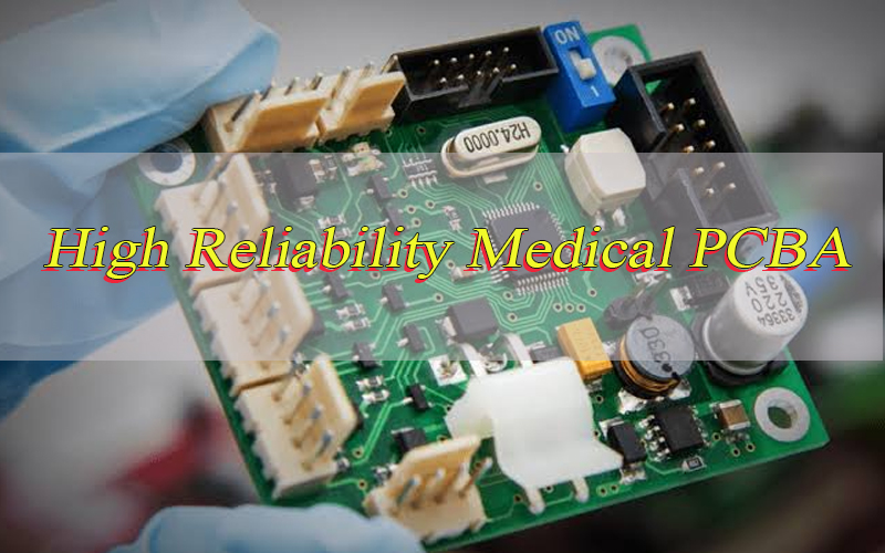
Automotive electronics PCB projects require stable materials, accurate fabrication, reliable soldering, complete inspection and repeatable batch quality. These boards are used in vehicle systems where heat, vibration, humidity, current load and long service life can affect final product reliability.

EBest Circuit provides automotive electronics PCB manufacturing and assembly services from a China source factory. We support prototype PCB, automotive PCB assembly, component sourcing, testing and batch production for global vehicle electronics projects.

Are you facing these production and assembly risks in automotive electronics PCB projects?

  • Do material shortages, unstable PCB materials, plating defects or impedance deviation delay your automotive electronics PCB production schedule?
  • Are BGA, QFN, connector, fine-pitch component or through-hole soldering defects increasing your automotive PCBA rework cost and approval risk?
  • Are BOM changes, component sourcing delays, testing requirements or hidden process costs making your final project budget harder to control?

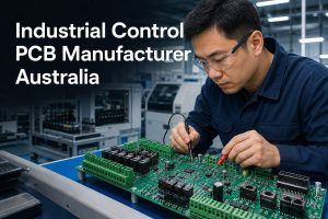
As a PCB manufacturer with 20+ years of experience, EBest Circuit provides automotive electronics PCB manufacturing and assembly support for vehicle electronics brands, OEM projects, EMS companies and technical teams. Below are our solutions to above problems:

  • Manufacturing control: We review Gerber files, stack-up, copper thickness, material selection, impedance requirements and panel design before production to reduce fabrication defects and batch instability.
  • Assembly reliability: We support BOM review, component sourcing, stencil design, SMT assembly, through-hole assembly, AOI inspection and X-ray inspection to reduce soldering defects and PCBA rework.
  • Cost and delivery control: We confirm fabrication, assembly, testing, coating, programming, packaging and shipment requirements before production to reduce hidden costs, repeated revisions and delivery risks.

Welcome to contact EBest Circuit if you need automotive electronics PCB manufacturing and assembly support: sales@bestpcbs.com.

Automotive Electronics PCB, https://www.bestpcbs.com/blog/2026/07/automotive-electronics-pcb/

What Is an Automotive Electronics PCB?

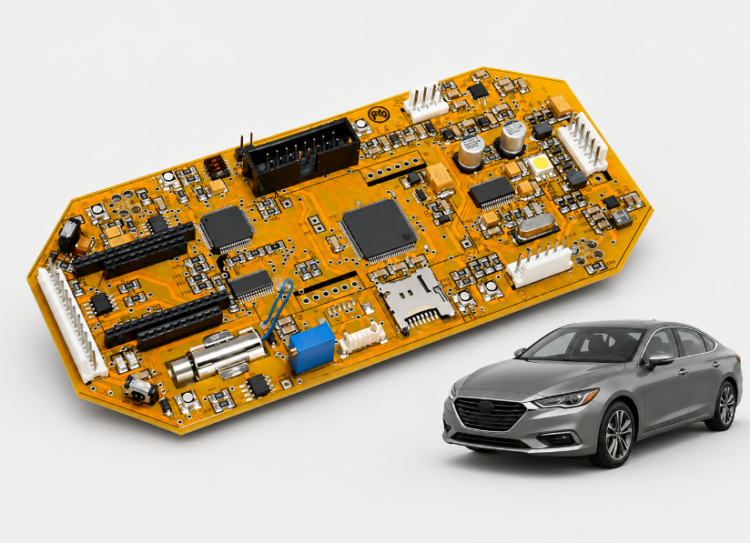
An automotive electronics PCB is a printed circuit board used in vehicle electronic systems to connect, support and control electronic components. It must operate reliably under vibration, heat, humidity, electrical load and long service cycles.

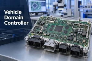
These PCBs are commonly used in body control modules, lighting systems, BMS boards, sensors, infotainment systems, power control units and ADAS-related modules. Compared with simple consumer electronics boards, automotive boards need stronger material control, better process stability and more complete testing.

For vehicle electronics projects, the main concern is not only whether the board can be produced. The more important question is whether the supplier can keep the same reliability from prototype to repeat batch production.

Why Is Automotive Electronics PCB Manufacturing Different from Standard PCB Manufacturing?

Automotive electronics PCB manufacturing is different because vehicle electronics face harsher working conditions and stricter reliability expectations. Standard PCB production may focus mainly on electrical connection, while automotive PCB manufacturing must also control thermal stress, vibration, long-term aging and traceability.

Main differences include:

  • Wider temperature conditions: Materials must resist thermal cycling, soldering heat and long-term operating stress.
  • Higher vibration risk: Connectors, solder joints and plated holes must remain mechanically stable.
  • Longer service life: Vehicle electronics often need many years of stable operation.
  • Stricter inspection: AOI, X-ray, electrical testing and functional testing are often combined.
  • Better traceability: Material lots, process records and inspection data should be controlled.

For this reason, automotive PCB projects should be reviewed before tooling, not after production problems appear.

What Are the Main Applications of Automotive Electronics PCB?

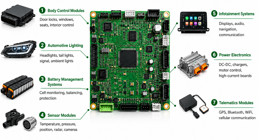
Automotive electronics PCB applications cover control, lighting, sensing, power, communication and safety-related vehicle systems. Each application has different requirements for copper thickness, material, thermal design, impedance and assembly quality.

In most vehicle electronics projects, common applications include:

  • Body control modules: Door locks, window control, seat control and interior electronics.
  • Automotive lighting: LED headlights, tail lights, signal lights and ambient lighting.
  • Battery management systems: Cell monitoring, balancing circuits and protection boards.
  • Sensor modules: Temperature, pressure, position, radar and camera-related electronics.
  • Infotainment systems: Display boards, audio modules, navigation and communication interfaces.
  • Power electronics: DC-DC converters, charging modules, motor control and high-current boards.
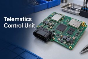
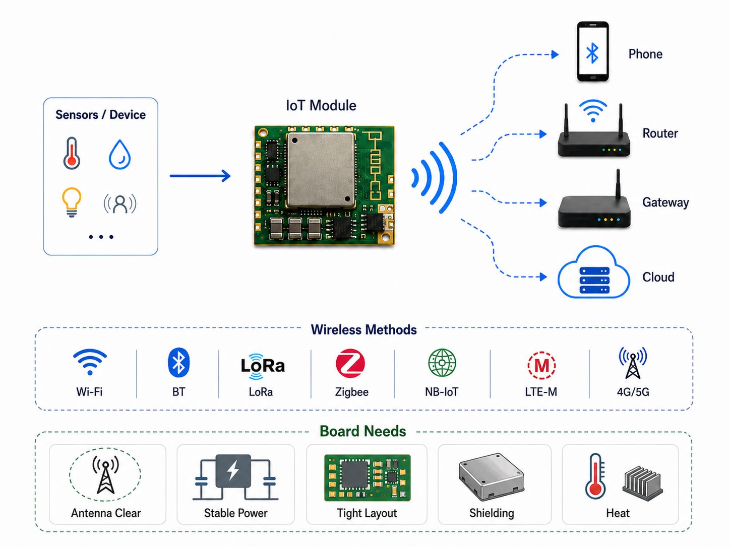
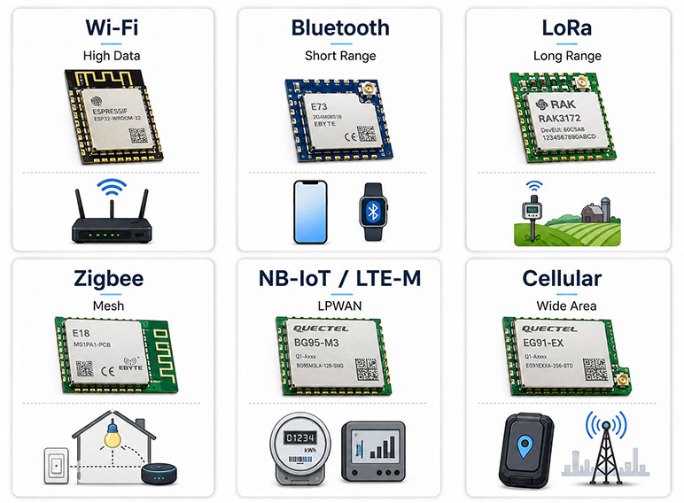
  • Telematics modules: GPS, Bluetooth, WiFi, cellular and vehicle communication systems.
Automotive Electronics PCB application, https://www.bestpcbs.com/blog/2026/07/automotive-electronics-pcb/

Which PCB Materials Are Commonly Used in Automotive Electronics?

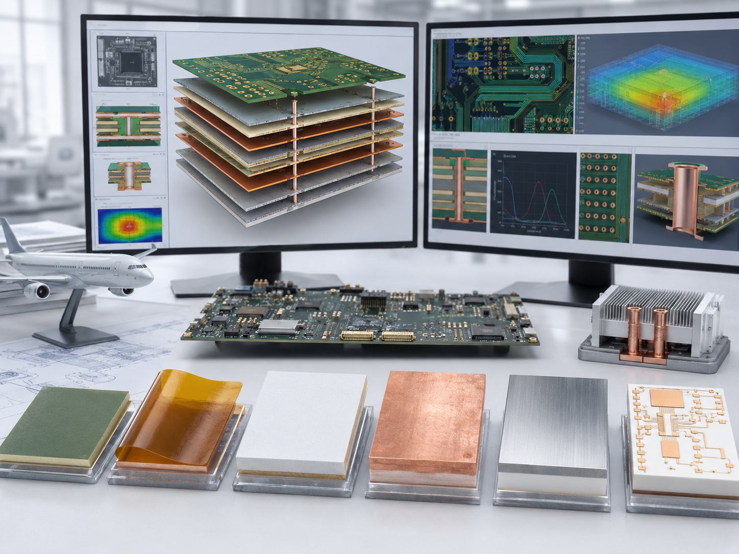
Common automotive PCB materials include FR4, High-Tg FR4, aluminum substrate, polyimide, rigid-flex materials and low-loss laminates. Heavy copper is also common in power boards, but it is a copper thickness option, not a base material.

MaterialTypical UseCommon RangeMain Benefit
FR4Body control, sensors, infotainment, general control boardsTg 130–170°CCost-effective and widely available
High-Tg FR4Engine bay electronics, multilayer boards, power modulesTg 170°C+Better heat resistance
Aluminum substrateLED headlights, tail lights, thermal modules1.0–2.0 W/m·K typical thermal conductivityStrong heat dissipation
PolyimideFlexible PCB, rigid-flex PCB, compact modulesTg 200°C+Better bending and thermal resistance
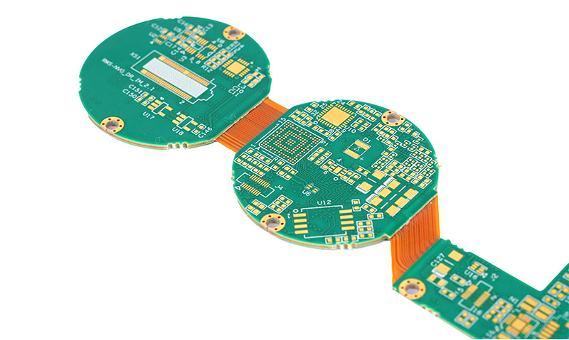
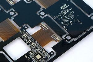
Rigid-flex materialsCamera modules, sensors, compact control systemsProject-specific stack-upSaves space and reduces connector risk
Low-loss laminateRadar, RF, ADAS and high-speed communication boardsLow Dk / low Df gradeImproves signal stability
Heavy copper structureBMS, DC-DC converters, motor control and high-current boards2–6 oz copper or higherImproves current capacity

What Are the Design Requirements for Automotive Electronics PCB?

Automotive electronics PCB design should focus on electrical stability, heat control, EMI reduction, vibration resistance and manufacturability. A reliable design can reduce prototype revisions, assembly defects and long-term field failure risks.
  • Current capacity: Power traces should use enough line width, copper thickness and copper area. For BMS, motor control, lighting and charging modules, high-current paths should be reviewed together with via quantity and heat dissipation.
  • Thermal management: Heat-generating components should be placed near copper planes, thermal vias, heat sinks or aluminum substrate areas. Poor thermal paths may cause LED brightness decay, component aging, solder fatigue or board deformation.
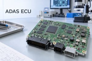
  • Signal integrity: High-speed, RF, camera, radar and communication lines should control impedance, return paths, trace length and layer transitions. For compact ADAS and sensor modules, fine-line HDI layouts should be reviewed carefully.
  • EMI and grounding: Ground planes should be stable and return paths should be short. Noisy power circuits, RF circuits and sensitive signal areas should be separated to reduce interference, unstable communication and testing failure.
  • Mechanical strength: Connectors, mounting holes, large components and heavy parts should avoid weak board edges or narrow breakaway areas. Automotive PCBA may face vibration, insertion force and long-term mechanical stress.
  • Assembly reliability: Pad size, solder mask clearance, stencil opening, component spacing and test point access should be checked before production. Good DFA review helps reduce solder bridges, tombstoning, poor wetting and rework.
  • Material and stack-up matching: Material, layer count, copper thickness and surface finish should match the application environment. High-Tg FR4, aluminum substrate, polyimide, rigid-flex materials or low-loss laminates may be selected according to heat, bending or signal requirements.
  • Testing access: Test points should be reserved for flying probe testing, ICT, functional testing or programming. Without enough test access, fault diagnosis becomes slower and batch production approval may be delayed.

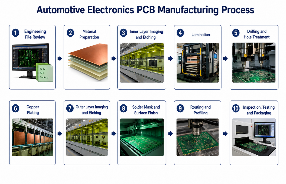
How Does the Automotive Electronics PCB Manufacturing Process Work?

The automotive electronics PCB manufacturing process starts with engineering review and ends with inspection, electrical testing and controlled packaging. Each step must be controlled because small defects in drilling, plating, solder mask or surface finish may affect long-term vehicle reliability.

Step 1: Engineering file review.
The production team checks Gerber files, drill files, stack-up, copper thickness, impedance requirements, material selection, surface finish and tolerance requirements. DFM feedback is provided before production to reduce design and fabrication risks.
Step 2: Material preparation.
Laminate, copper foil, prepreg, solder mask and surface finish requirements are prepared according to the confirmed specification. Material type, thickness, Tg, copper weight and batch information should match the project requirements.

Step 3: Inner layer imaging and etching.
For multilayer automotive PCB, inner layers are imaged, etched and inspected first. AOI is used to check line width, spacing, shorts, opens and circuit accuracy before lamination.

Step 4: Lamination.
Inner layers, prepreg and copper foil are pressed together under controlled temperature, pressure and time. Stable lamination helps reduce delamination, warpage and layer misalignment.

Step 5: Drilling and hole treatment.
Mechanical drilling or laser drilling creates through holes, vias or microvias. Desmear and hole cleaning are then performed to prepare reliable copper plating inside the holes.

Step 6: Copper plating.
Copper is plated onto hole walls and board surfaces to build electrical connections between layers. Plating thickness and hole wall quality are important for vibration resistance and long-term reliability.

Step 7: Outer layer imaging and etching.
The outer circuit pattern is transferred, plated and etched. This step controls final trace width, spacing, pads and copper features.

Step 8: Solder mask and surface finish.
Solder mask is applied to protect copper and define soldering areas. ENIG, OSP, immersion silver or lead-free HASL can be selected according to solderability, storage time and assembly requirements.

Step 9: Routing and profiling.
The PCB is routed, scored or shaped according to the board outline and panel design. Mounting holes, slots and edge quality are checked to support final assembly.

Step 10: Inspection, testing and packaging.
AOI, electrical testing, impedance testing when required, visual inspection and final quality checks are completed before shipment. Boards are packaged with labels and traceability records according to project requirements.

Automotive Electronics PCB Manufacturing Process, https://www.bestpcbs.com/blog/2026/07/automotive-electronics-pcb/

How Does Automotive Electronics PCB Assembly Work?

Automotive electronics PCB assembly turns a bare PCB into a tested PCBA through component sourcing, solder paste printing, SMT placement, reflow soldering, inspection and final testing. Each step must be controlled because solder defects, wrong components or weak testing may affect vehicle electronics reliability.

Step 1: BOM review and component sourcing.
The BOM is checked for part numbers, package sizes, temperature grade, lifecycle status, lead time and approved alternatives. This helps reduce sourcing delays, wrong substitutions and assembly risks before production starts.

Step 2: Stencil and solder paste preparation.
The stencil opening is designed according to pad size, component type and solder volume requirements. Proper solder paste control helps reduce solder bridges, insufficient solder, tombstoning and poor wetting.

Step 3: SMT placement.
SMT machines place resistors, capacitors, ICs, sensors, connectors, BGA, QFN and other components onto the PCB. Placement accuracy is important for fine-pitch components and compact automotive electronics PCB assembly.

Step 4: Reflow soldering.
The assembled board passes through a controlled reflow profile. Temperature control helps protect components, improve solder joint strength and reduce defects caused by overheating or insufficient heating.

Step 5: AOI and X-ray inspection.
AOI checks visible defects such as missing parts, polarity errors, misalignment and solder bridges. X-ray inspection is used for BGA, QFN and bottom-terminated components where solder joints cannot be seen from the surface.

Step 6: Through-hole and mixed assembly.
Connectors, terminals, relays, transformers or high-power parts may require wave soldering, selective soldering or manual soldering. These parts need stronger process control because they often face vibration and insertion force.

Step 7: ICT, functional testing and programming.
ICT checks circuit connection and component placement, while functional testing confirms real operating performance. Programming, calibration, conformal coating or box-build assembly can be added according to project requirements.

What Automotive PCB Manufacturing and Assembly Services Does EBest Circuit Provide?

EBest Circuit provides one-stop automotive PCB manufacturing and assembly services from prototype to batch production. We support PCB fabrication, component sourcing, SMT assembly, through-hole assembly, BGA assembly, testing and box assembly for vehicle electronics projects.

Our services include:

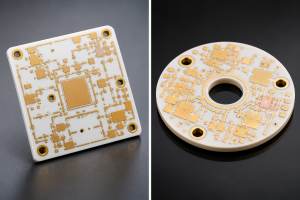
  • PCB fabrication: FR4 PCB, multilayer PCB, metal-based PCB, ceramic PCB, flexible PCB, rigid-flex PCB and high-frequency PCB.
  • Prototype and quick-turn PCB: Prototype PCB, low-volume production and urgent PCB orders with fast response.
  • Automotive PCB assembly: SMT assembly, THT assembly, mixed assembly, BGA assembly, flex PCB assembly and turnkey PCB assembly.
  • Component sourcing: Support for SMD, BGA, QFN, QFP and other electronic components through a stable supply chain.
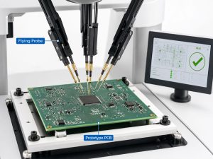
  • Testing and inspection: AOI, X-ray inspection, flying probe testing, ICT, functional testing and final inspection before delivery.
  • Box assembly: Final assembly, labeling, packaging and 100% inspection before shipment when required.

EBest Circuit can handle 01005 SMD components, 0.25mm minimum BGA pitch, SMT/THT mixed assembly and 1–5 days lead time for selected PCBA projects.

Quality Control for Automotive PCB and PCBA Orders: From Materials to Final Testing

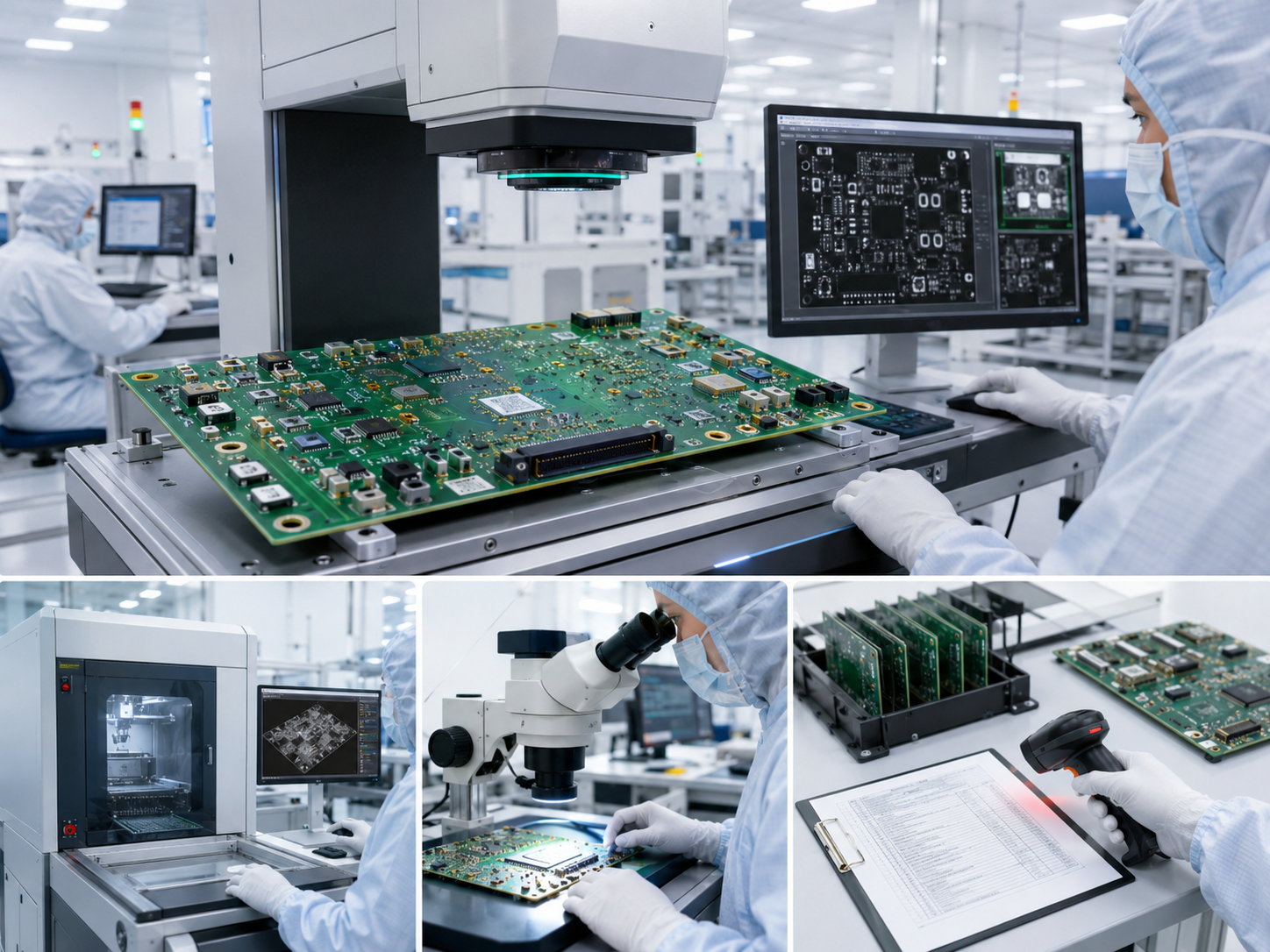
Automotive PCB and PCBA quality control should cover materials, fabrication, assembly, testing, traceability and shipment inspection. Final testing alone is not enough because many reliability risks start from material selection, drilling, plating, soldering or component handling.

  • Material inspection: Laminate, copper foil, solder mask, prepreg and surface finish materials are checked against the confirmed specification. Material type, thickness, Tg, copper weight and batch records should match the project requirements.
  • Inner layer inspection: For multilayer automotive PCB, inner circuits are inspected before lamination. AOI checks line width, spacing, shorts, opens and pattern accuracy to reduce hidden layer defects.
  • Drilling and plating control: Hole size, registration, desmear quality and copper plating thickness are controlled carefully. Reliable hole wall copper is important for vibration resistance, thermal cycling and long-term electrical connection.
  • Solder mask and surface finish inspection: Solder mask coverage, opening accuracy, adhesion and surface finish quality are checked before assembly. Poor solder mask or surface finish may cause soldering defects, oxidation or poor wetting.
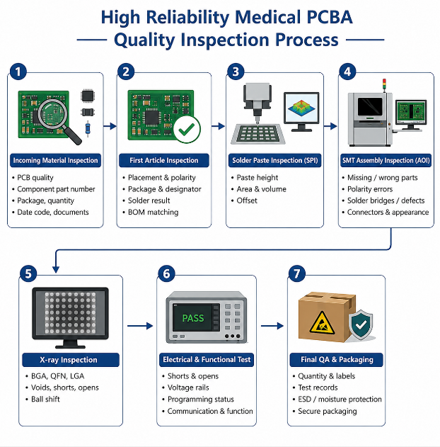
  • SMT process inspection: SPI can check solder paste volume before placement. AOI checks component polarity, missing parts, alignment, solder bridges and visible solder defects after reflow.
  • Hidden solder joint inspection: X-ray inspection is used for BGA, QFN, BTC and other hidden solder joints. This helps identify voids, insufficient solder, bridging and weak solder connections.
  • Electrical and functional testing: Flying probe testing, ICT and functional testing can be selected according to project needs. These tests help confirm circuit continuity, component operation and final PCBA performance.
  • Traceability and final shipment control: Material records, production batches, inspection data, labels and packaging details are controlled before shipment. This supports repeat orders, quality tracking and long-term automotive electronics PCB production.

Automotive Electronics PCB Assembly Case Study: From Prototype to Reliable Batch Production

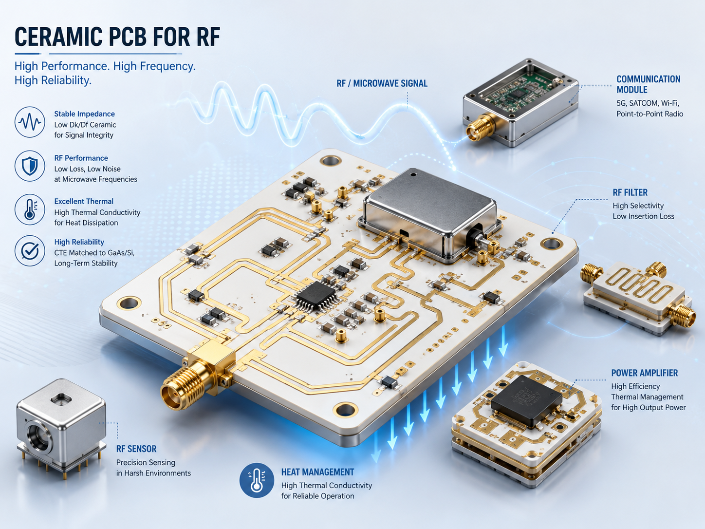
A reliable automotive electronics PCBA project should move from prototype validation to stable batch production through design review, process control, testing planning and production record management. The following case shows how early review can reduce assembly risk and improve repeatability.

Project background:
A vehicle control module required stable signal transmission, reliable connector strength and long-term solder joint performance. The first prototype design had tight component spacing, limited test points and insufficient copper area around several power components.

Project requirements:
The PCBA needed stable automotive electronics PCB manufacturing, accurate SMT assembly, reliable connector soldering and complete testing before batch approval. The project also required BOM review, X-ray inspection for hidden solder joints, functional testing and controlled packaging for repeat orders.

Our solution:
EBest Circuit reviewed the PCB layout, stack-up, solder mask clearance, copper balance, connector footprint and test point access before production. During assembly, we supported BOM review, component sourcing, stencil design, SMT placement, reflow control, AOI inspection and X-ray inspection to reduce soldering and assembly risks.
Final result:
After prototype validation, the production process, testing method, inspection records and packaging requirements were confirmed for batch manufacturing. The project achieved more stable PCBA assembly, fewer repeated revisions and better consistency for later automotive electronics PCB production.

Automotive Electronics PCB Assembly, https://www.bestpcbs.com/blog/2026/07/automotive-electronics-pcb/

Why Choose EBest Circuit for Automotive Electronics PCB Manufacturing and Assembly?

EBest Circuit helps automotive electronics projects reduce supplier coordination, production risk, assembly defects and delivery uncertainty. From PCB fabrication to component sourcing, PCBA assembly, testing and box assembly, one-stop support makes prototype and batch production easier to control.

Choose EBest Circuit because:

  • Reduce supplier management time: PCB fabrication, component sourcing, SMT assembly, THT assembly, BGA assembly, testing and box assembly can be handled together, reducing communication between multiple suppliers.
  • Lower manufacturing risk: Gerber files, stack-up, copper thickness, material selection, impedance requirements and panel design are reviewed before production to reduce fabrication defects and batch instability.
  • Improve assembly reliability: Support for 01005 SMD components, 0.25mm minimum BGA pitch, SMT/THT mixed assembly and BGA assembly helps manage compact automotive PCBA projects with fine-pitch components.
  • Control component sourcing delays: A stable component supply chain supports SMD, BGA, QFN, QFP and other electronic components, helping reduce BOM delays and unplanned substitutions.
  • Shorten project lead time: Selected urgent PCB orders can be shipped within 24 hours, and selected PCBA projects can support 1–5 days lead time depending on complexity and material readiness.
  • Support repeat batch production: Process control, inspection records, final testing and packaging control help keep prototype approval, pilot run and batch production more consistent.

If your project needs automotive electronics PCB manufacturing and assembly with controlled cost, reliable inspection and practical production support, EBest Circuit can review your files and provide a quotation.

FAQs About Automotive Electronics PCB

Q1: What is the biggest risk in automotive electronics PCB production?
A1: The biggest risk is hidden reliability failure after delivery. Automotive PCB may pass a basic electrical test but still fail later because of weak solder joints, poor via plating, thermal stress, vibration, contamination or unsuitable material selection.

Q2: What certifications are important for automotive PCB manufacturing?
A2: IATF 16949 and ISO 9001 are important for automotive PCB quality control. Depending on the project, ISO 13485, AS9100D, UL, RoHS and REACH may also support compliance, traceability and market access requirements.

Q3: Does EBest Circuit support automotive PCB assembly?
A3: Yes. EBest Circuit supports SMT assembly, THT assembly, mixed assembly, BGA assembly, prototype PCB assembly, quick-turn PCB assembly and full turnkey PCB assembly. Component sourcing, testing and box assembly can also be added when required.

Q4: What PCB types can be used in automotive electronics?
A4: Common options include FR4 PCB, multilayer PCB, metal-based PCB, ceramic PCB, flexible PCB, rigid-flex PCB and high-frequency PCB. The right choice depends on heat, vibration, space, current load, signal speed and cost requirements.

Q5: Can automotive PCB projects use BGA components?
A5: Yes. BGA components are common in compact control modules, communication boards and high-performance automotive PCBA. EBest Circuit supports BGA assembly and X-ray inspection to check hidden solder joints that cannot be inspected visually.

Q6: What is the minimum BGA pitch EBest Circuit can support?
A6: EBest Circuit supports 0.25mm minimum BGA pitch. For fine-pitch BGA projects, stencil design, reflow profile, PCB flatness, pad design and X-ray inspection should be reviewed before batch production.

Q7: What is the minimum SMD component size supported?
A7: EBest Circuit supports 01005 minimum SMD components. For small components, solder paste control, placement accuracy, reflow profile and AOI inspection are important to reduce tombstoning, shifting and insufficient solder.

Q8: How fast can automotive PCB or PCBA orders be delivered?
A8: Selected urgent PCB orders can be shipped within 24 hours, and PCBA lead time can be 1–5 days depending on project complexity. Material availability, BOM status, testing requirements and order quantity will affect the final delivery schedule.

Q9: Can EBest Circuit provide full turnkey automotive PCBA?
A9: Yes. Full turnkey PCBA can include PCB fabrication, component sourcing, SMT assembly, THT assembly, BGA assembly, inspection, testing, packaging and shipment. This helps reduce supplier coordination and project management time.

Q10: Why choose a China source factory for automotive PCB projects?
A10: A China source factory can support custom PCB fabrication, component sourcing, flexible production volume and cost control in one supply chain. EBest Circuit also supports global delivery without false local factory or overseas warehouse claims.

Q11: How can soldering defects in automotive PCBA be reduced?
A11: Soldering defects can be reduced through stencil review, solder paste control, accurate SMT placement, reflow profile control, AOI inspection and X-ray inspection. BGA, QFN, connectors and fine-pitch parts should receive extra process attention.

Q12: Does automotive PCB assembly require functional testing?
A12: Functional testing is strongly recommended when the PCBA must meet real operating requirements. ICT can check circuit connection, while functional testing confirms whether the assembled board performs correctly under the required working conditions.

Q13: How do I choose an automotive electronics PCB manufacturer?
A13: Choose a manufacturer with PCB fabrication, PCBA assembly, component sourcing, testing capability, quality certifications and traceability control. For automotive electronics, stable production and inspection capability matter more than only low unit price.

Automotive electronics PCB projects need stable materials, controlled fabrication, reliable assembly, complete testing and repeatable batch quality. The right supplier should support PCB manufacturing, component sourcing, SMT assembly, BGA inspection, functional testing and final delivery together, so production risks can be found earlier and controlled before shipment.

EBest Circuit provides automotive electronics PCB manufacturing and assembly services from a China source factory, supporting prototype, low-volume and batch PCBA projects for global vehicle electronics applications. If you need automotive PCB fabrication, component sourcing, PCBA assembly, testing or box assembly, send your Gerber files, BOM, quantity and testing requirements for quotation: sales@bestpcbs.com.

You may also like

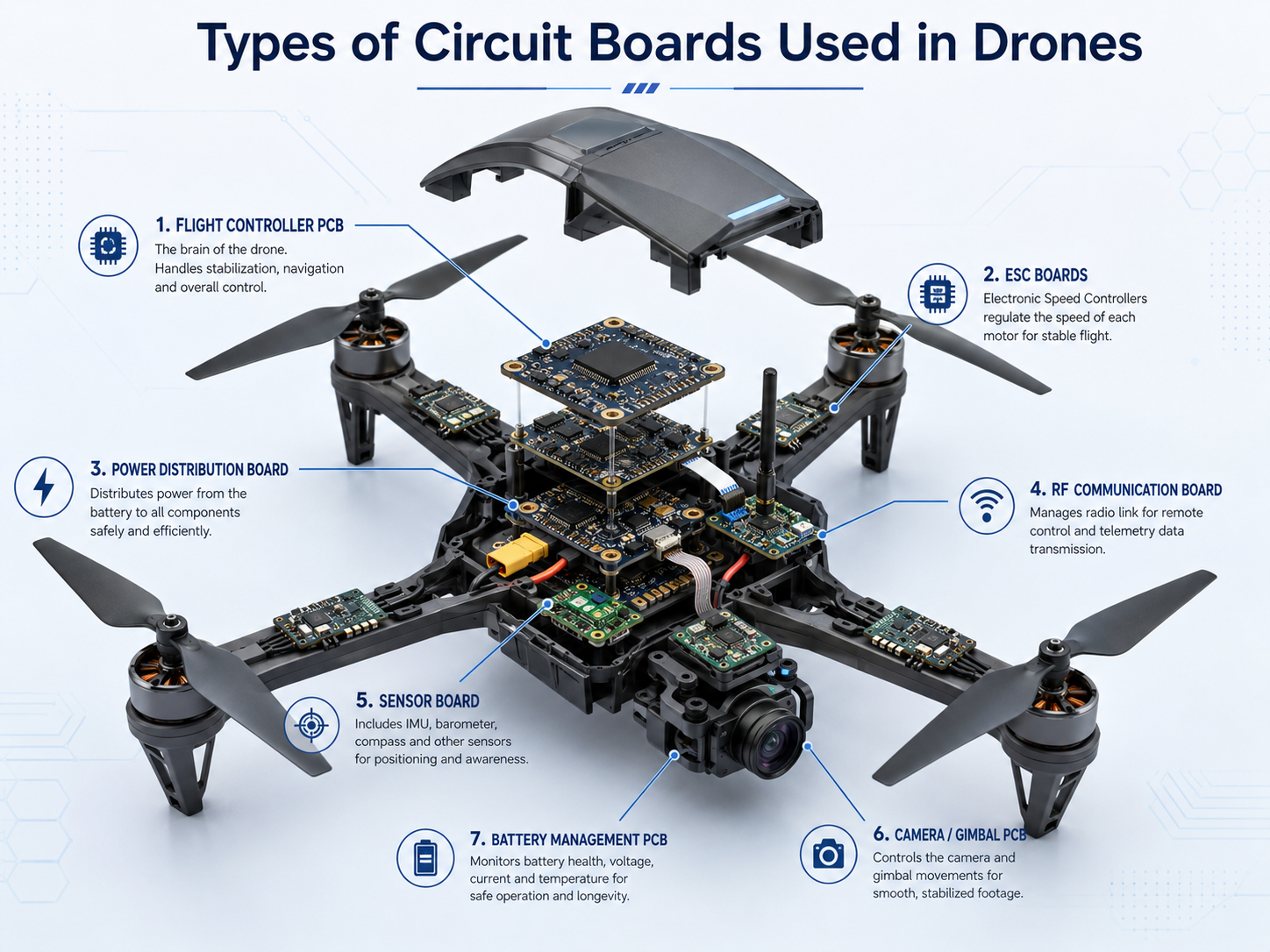
Types of Circuit Boards Used in Drones: UAV PCB Guide

June 26th, 2026

The main types of circuit boards used in drones include flight controller PCBs, ESC boards, power distribution boards, RF communication boards, sensor boards, camera and gimbal boards, battery management boards, flexible PCBs, rigid-flex PCBs, HDI PCBs, and high-current power PCBs. Each board supports a different task: stable flight, motor control, power delivery, image transmission, navigation, sensing, or system integration.

A drone is not controlled by one single board. It is a compact electronic system where weight, vibration, heat, current, signal noise, and mechanical space all affect PCB selection. Choosing the right PCB structure helps improve flight stability, reduce assembly risk, and extend service life in real operating environments.

Types of Circuit Boards Used in Drones: UAV PCB Guide

What Are the Types of Circuit Boards Used in Drones?

The types of circuit boards used in drones are specialized PCBs designed for flight control, power conversion, motor driving, communication, sensing, imaging, and battery protection. A consumer camera drone, FPV racing drone, agricultural UAV, and industrial inspection drone may all use different PCB combinations.

In simple terms, a drone PCB carries signals and power between the battery, processor, sensors, motors, receiver, camera, and communication modules. Some boards handle low-voltage logic. Others carry high-current motor power. High-end drones may use rigid-flex or HDI PCB structures to reduce connectors, save weight, and fit complex mechanical layouts.

Board TypeMain FunctionCommon Location in DroneTypical Design Focus
Flight controller PCBControls flight attitude and stabilityCentral bodySignal integrity, IMU placement, vibration control
ESC PCBDrives brushless motorsArm area or integrated stackHigh current, heat dissipation, MOSFET layout
Power distribution boardDistributes battery powerCentral frame or stackCopper thickness, current path, voltage drop
Sensor PCBCollects motion, altitude, GPS, optical dataBody, bottom, or navigation moduleNoise control, stable reference ground
RF communication PCBHandles control, telemetry, GPS, Wi-Fi, and videoAntenna or communication moduleImpedance control, shielding, RF material
Camera and gimbal PCBSupports video, image sensor, and stabilizationCamera module or gimbalHigh-speed signal, flexible connection
BMS PCBProtects the battery packBattery moduleCurrent sensing, protection, thermal design
Rigid-flex PCBConnects moving or folded partsArms, gimbal, camera, compact bodyReliability, space saving, bend control
HDI PCBSupports compact high-density electronicsFlight controller, camera, AI moduleFine lines, microvias, compact routing

Why Are Drone Circuit Boards Important for Flight Reliability?

Drone circuit boards are important because they directly affect flight control, power stability, signal accuracy, and long-term reliability. A small layout issue can create unstable sensor readings, motor noise, voltage drop, overheating, or communication loss.

Unlike many static electronics, drones face constant vibration, rapid current changes, airflow cooling differences, outdoor humidity, impact shock, and compact assembly pressure. The PCB must remain electrically stable while the frame moves and motors generate noise. This is why a drone board should be treated as both an electronic component and a structural reliability component.

For example, the flight controller board must keep the IMU sensor clean from vibration and electrical noise. The ESC board must handle pulsed current without overheating. RF boards must maintain signal quality near motors, batteries, and carbon-fiber frames. Each PCB has a clear job, and each job affects flight safety.

Why Are Drone Circuit Boards Important for Flight Reliability?

How Do Drone PCBs Work Inside a UAV System?

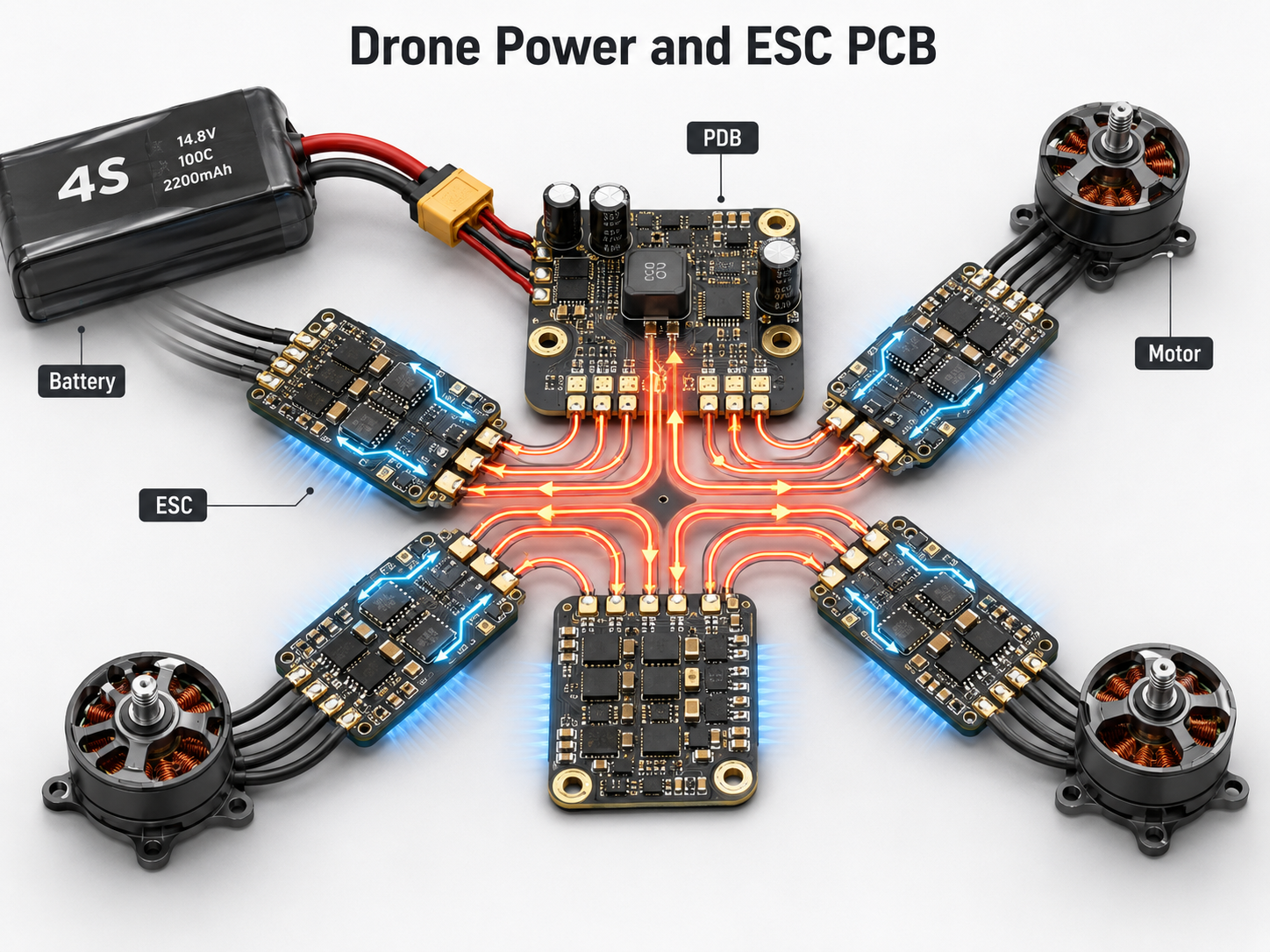
Drone PCBs work by connecting control signals, power rails, sensors, motor drivers, and communication modules into one coordinated UAV system. The flight controller receives data from sensors, calculates attitude corrections, and sends commands to the ESCs. The ESCs then drive the motors according to those commands.

Power usually starts from a lithium battery pack. It passes through a power distribution board, BMS, voltage regulator, or integrated AIO board. Low-voltage rails power the MCU, receiver, GPS, IMU, barometer, camera, and telemetry module.

A stable drone PCB system needs clean separation between noisy power circuits and sensitive signal circuits. Good grounding, layer stack-up, short return paths, shielding, and controlled impedance all help the drone process data accurately during flight.

Main Types of Circuit Boards Used in Drones

The main types of circuit boards used in drones can be divided by function and PCB construction. Function tells you what the board does. Construction tells you how the board is built.

Flight controller PCB is the brain of the drone. It carries the MCU, IMU, barometer, memory, connectors, and power regulation circuits.

ESC PCB converts control signals into three-phase motor drive output. It usually includes MOSFETs, gate drivers, current sensing, capacitors, and thermal copper areas.

Power distribution board distributes battery current to ESCs and other modules. Some drones use a separate PDB, while compact drones may integrate it into the flight controller or ESC stack.

Sensor PCB supports GPS, compass, optical flow, ultrasonic, LiDAR, airspeed, or environmental sensing.

Communication PCB handles receiver signals, telemetry, Wi-Fi, Bluetooth, RF links, GPS, or video transmission.

Camera and gimbal PCB supports image sensors, motors, video signals, and flexible connections across moving joints.

BMS PCB protects battery packs through over-current, over-voltage, under-voltage, temperature, and balancing functions.

AIO PCB combines several functions, such as flight controller, ESC, PDB, receiver, or video transmitter, into one compact board.

What PCB Materials Are Used in Drone Electronics?

Drone electronics commonly use FR4, high-Tg FR4, flexible polyimide, rigid-flex structures, metal core substrates, high-frequency laminates, and sometimes ceramic substrates for special thermal or RF applications. The material choice depends on weight, current, heat, frequency, bending, and cost.

FR4 is widely used because it offers good mechanical strength, stable processing, and reasonable cost. High-Tg FR4 is preferred when the drone board faces higher operating temperature or dense multilayer assembly. Flexible polyimide is useful in camera modules, gimbals, foldable arms, and compact sensor routing. Rigid-flex PCB is selected when the design needs fewer connectors and better vibration resistance.

For RF modules, controlled dielectric properties matter more. For high-current ESC or power boards, copper thickness, thermal vias, copper balance, and heat spreading become more important than simple material naming.

Material or StructureTypical Drone UseStrengthLimitation
Standard FR4Flight controller, sensor board, receiver boardCost-effective and stableLimited thermal performance for high-power zones
High-Tg FR4ESC, dense multilayer controller, industrial UAV boardsBetter thermal enduranceHigher cost than standard FR4
Flexible polyimide PCBGimbal, camera, foldable modulesLightweight and bendableNeeds bend radius control
Rigid-flex PCBCompact UAV systems, camera drones, industrial dronesReduces cables and connectorsHigher fabrication cost
HDI PCBMini flight controller, AI camera module, high-density system boardHigh routing densityRequires tighter DFM control
Metal core PCBLED, power, thermal modulesStrong heat spreadingLess suitable for complex multilayer signal routing
RF laminateGPS, telemetry, video transmissionBetter high-frequency performanceHigher material and process cost
Ceramic PCBHigh-power or special thermal modulesHigh thermal conductivity and insulationHigher cost and application-specific use

Key Features, Advantages, and Limitations of Drone PCBs

Drone PCBs are designed for lightweight assembly, reliable power delivery, stable signal processing, and resistance to vibration. Their advantages come from integration. A well-designed board can reduce wires, save space, simplify assembly, and improve electrical performance.

The main limitation is design compromise. A drone PCB often has to balance weight, current capacity, heat dissipation, RF performance, mechanical strength, and cost in a small area. Increasing copper thickness helps current capacity but adds weight and may affect etching precision. Adding more layers improves routing and shielding but raises cost. Choosing rigid-flex saves connector space but requires stricter fabrication and assembly control.

The best PCB choice is rarely the most advanced option. It is the structure that matches the drone’s payload, flight time, motor current, communication distance, sensor accuracy, and production volume.

Rigid PCB vs Flexible PCB vs Rigid-Flex PCB vs HDI PCB for Drones

Rigid PCB, flexible PCB, rigid-flex PCB, and HDI PCB solve different drone design problems. Rigid PCB is suitable for stable flat assemblies. Flexible PCB is useful for motion and tight routing. Rigid-flex PCB improves reliability by replacing connectors. HDI PCB supports compact high-density designs.

PCB TypeBest ForTypical Drone ExampleRelative CostMain Design Concern
Rigid PCBStandard flat electronic modulesFlight controller, ESC, receiverLow to mediumLayer stack-up, vibration, thermal balance
Flexible PCBMoving or narrow spacesCamera, gimbal, foldable armsMediumBend radius, stiffener, copper cracking
Rigid-flex PCBCompact and vibration-prone systemsIndustrial UAV, camera drone, aerospace-style UAV moduleHighStack-up transition, impedance, assembly yield
HDI PCBMiniaturized high-density electronicsSmall flight controller, AI vision module, advanced camera boardHighMicrovia reliability, fine-line manufacturing
Metal core PCBHeat-heavy modulesLED, power, high-current thermal boardMedium to highInsulation layer, thermal path, mechanical fit

For most standard drones, multilayer FR4 PCBs remain practical. For compact camera drones and high-end industrial UAVs, rigid-flex and HDI designs often provide better space efficiency and reliability.

How to Choose the Right Drone Circuit Board for Your Project

Choose a drone circuit board by matching the board function with electrical load, mechanical space, vibration level, signal speed, operating environment, and production volume. Start from the drone’s mission, then define PCB requirements.

For FPV racing drones, weight, high-current ESC performance, compact AIO design, and vibration resistance are key. For camera drones, signal quality, gimbal flex life, image module routing, and compact packaging matter more. For agricultural drones, current handling, moisture resistance, connector strength, and serviceability are more important. For inspection drones, reliability, long flight time, RF stability, and rugged assembly often lead the design.

Project NeedRecommended PCB DirectionReason
Small FPV droneAIO PCB, HDI PCB, high-Tg FR4Saves space and weight
Long-range UAVControlled impedance RF PCB, stable power boardImproves communication and telemetry reliability
Camera droneRigid-flex PCB, flex PCB, HDI camera boardSupports compact moving modules
Heavy-lift droneHigh-current ESC PCB, thick copper PDBHandles motor current and thermal stress
Industrial inspection UAVRigid-flex or multilayer FR4 with strong QCImproves vibration and field reliability
Outdoor agricultural droneConformal coating, robust connectors, high-current designHandles moisture, load, and field service conditions

Where Are Drone PCBs Used Across Different UAV Applications?

Drone PCBs are used in consumer drones, FPV racing drones, industrial inspection drones, agricultural UAVs, mapping drones, logistics drones, public safety drones, research UAVs, and robotics platforms. Each application puts a different priority on the circuit board.

Consumer drones value compact size, stable camera transmission, clean power, and consistent assembly. FPV drones value low weight, fast response, and high-current ESC performance. Industrial drones need stronger reliability under vibration, temperature changes, and long operating hours. Agricultural drones need robust high-current power delivery and environmental protection. Mapping drones need stable GPS, camera, and storage interfaces.

Drone PCB Design Guidelines for Weight, Power, EMI, and Vibration

Drone PCB design should balance four core factors: weight, power, EMI, and vibration. These factors decide whether the board performs well in real flight conditions.

For weight control, avoid oversized boards, unnecessary connectors, excessive copper where it is not needed, and overbuilt layer counts. For power delivery, keep high-current paths short and wide, use suitable copper thickness, apply thermal vias where needed, and avoid narrow neck-downs near MOSFETs or battery inputs.

For EMI control, separate motor power circuits from IMU, GPS, RF, and analog sensing areas. Use continuous ground planes where possible, keep return paths short, and route high-speed or RF signals with impedance control. For vibration, use proper mounting holes, reinforced connectors, component placement awareness, and flexible interconnects where repeated motion occurs.

Common Drone PCB Failures and How to Prevent Them

Common drone PCB failures include overheated ESC circuits, cracked solder joints, connector fatigue, voltage drop, RF interference, IMU noise, moisture corrosion, and flexible circuit cracking. Most of these problems can be reduced during design review and manufacturing planning.

Failure ModeCommon CauseTypical SymptomPrevention Method
ESC overheatingPoor MOSFET layout, narrow copper, weak heat spreadingMotor cut-off, burnt componentsUse wider copper, thermal vias, copper balance, thermal simulation review
Voltage dropLong or narrow high-current pathsBrownout, unstable controller resetShorten power path, increase copper width and thickness, improve PDB layout
IMU noisePoor placement near vibration or switching circuitsDrift, unstable hover, flight correction errorsIsolate IMU area, improve grounding, separate noisy circuits
RF signal lossPoor antenna layout, impedance mismatch, motor EMIReduced control distance or video dropControlled impedance, shielding, antenna clearance
Cracked solder jointsVibration, heavy components, weak mountingIntermittent failureUse proper mounting, adhesive support where needed, strong inspection
Flex crackingTight bend radius or wrong stack-upCamera or gimbal signal lossDefine bend radius, use suitable copper, add stiffener
CorrosionMoisture, field exposure, flux residueLeakage, unstable signal, visible oxidationClean assembly, conformal coating, proper packaging
DelaminationHeat, material mismatch, poor process controlBlistering, open circuitsSelect proper Tg and material, control lamination and reflow profile

Failure analysis should look at the board as a system. A burnt ESC is not always a component problem. It may come from trace width, copper thickness, thermal relief design, solder voiding, airflow blockage, or motor load mismatch.

What Affects Drone PCB Cost and Procurement?

Drone PCB cost is affected by layer count, board size, material, copper thickness, line width and spacing, via structure, surface finish, impedance control, rigid-flex complexity, HDI microvias, assembly density, testing requirements, and order quantity.

A simple 2-layer or 4-layer FR4 drone board is usually more cost-effective than a rigid-flex or HDI design. However, cost should be evaluated by total system value, not only PCB unit price. A rigid-flex PCB may cost more per board, but it can reduce connectors, cables, manual assembly, and vibration-related failures. A thicker copper ESC PCB may also cost more, but it can improve thermal and current performance.

For purchasing teams, the best cost control method is early DFM review. Sending incomplete files often creates quotation changes later. Clear material, copper, finish, stack-up, tolerance, test, assembly, and packaging requirements help the supplier quote accurately.

How to Choose a Drone PCB Manufacturer and Prepare RFQ Files

Choose a drone PCB manufacturer that understands multilayer PCB fabrication, high-current layout risks, rigid-flex construction, impedance control, surface finish selection, PCBA assembly, and practical quality inspection. Drone boards are compact, but they are not simple.

RFQ ItemWhy It Matters
Gerber filesDefines copper, solder mask, silkscreen, drill, and board outline
Drill fileConfirms plated and non-plated holes
Stack-up requirementControls impedance, thickness, stiffness, and manufacturability
BOMSupports component sourcing and assembly review
Pick-and-place fileGuides SMT placement
Assembly drawingReduces connector orientation and polarity mistakes
Copper weightAffects current capacity, heat, cost, and etching
Surface finishAffects solderability, shelf life, and fine-pitch assembly
Impedance requirementNeeded for RF, video, USB, high-speed, and antenna circuits
Testing requirementDefines electrical test, AOI, X-ray, functional test, or programming
Application noteHelps engineers understand current, vibration, moisture, and use environment
Quantity and scheduleHelps balance prototype speed and mass production cost

EBest Circuit is a China source PCB and PCBA manufacturer supporting prototype, batch production, custom PCB fabrication, component sourcing, and assembly services. For drone projects, we can support FR4 PCB, high-Tg PCB, rigid-flex PCB, HDI PCB, metal core PCB, RF PCB, heavy copper PCB, and PCBA manufacturing according to project requirements.

Practical Case Scenarios for Drone Circuit Board Selection

A compact FPV drone often benefits from an AIO board that combines flight control, ESC, and power distribution. The main engineering focus is high-current routing, compact thermal design, clean sensor placement, and durable solder joints.

A camera drone often uses a rigid PCB for the main controller and flexible or rigid-flex boards for the camera and gimbal. This helps reduce cable bulk and supports motion between the body and camera system.

An agricultural drone usually needs stronger power boards, robust connectors, moisture protection, and careful thermal design. The board may look simple, but current load and field operation make reliability critical.

An industrial inspection drone may use multilayer PCB, controlled impedance communication boards, and rigid-flex interconnects. In this case, stable signal transmission and long-term vibration resistance often matter more than the lowest unit cost.

Frequently Asked Questions About Circuit Boards Used in Drones

Q1: What circuit board is the brain of a drone?

The flight controller PCB is usually called the brain of a drone. It processes sensor data from the IMU, barometer, GPS, receiver, and other modules, then sends control commands to the ESCs. A stable flight controller layout needs clean power, low noise, good grounding, and careful sensor placement.

Q2: What is the difference between a flight controller PCB and an ESC PCB?

A flight controller PCB calculates flight attitude and control commands, while an ESC PCB drives the motors. The flight controller handles logic and sensing. The ESC handles high-current switching, MOSFET control, and motor output. Both boards must work together for stable and responsive flight.

Q3: Do drones use rigid PCB or flexible PCB?

Drones can use both. Rigid PCB is common in flight controllers, ESCs, PDBs, and receiver boards. Flexible PCB is common in camera modules, gimbals, foldable arms, and tight spaces. Rigid-flex PCB combines both structures and is often selected when vibration resistance and compact assembly are important.

Q4: Why do some drones use rigid-flex PCBs?

Rigid-flex PCBs reduce cables and connectors, which helps save space and improve vibration resistance. They are useful in compact camera drones, foldable UAVs, and industrial drones with complex mechanical layouts. The main trade-off is higher manufacturing cost and stricter design control during stack-up and bend area planning.

Q5: What PCB material is best for drones?

There is no single best material for every drone. Standard FR4 works well for many control and sensor boards. High-Tg FR4 is better for warmer or denser boards. Polyimide is used for flex circuits. RF laminates support communication modules, while metal core or thicker copper structures help power and thermal boards.

Q6: How many layers does a drone PCB need?

Simple drone boards may use 2 layers, but many flight controllers and ESC boards use 4 layers or more. Compact integrated boards, HDI designs, and advanced camera or RF modules may need 6 layers, 8 layers, or higher. Layer count depends on routing density, power integrity, EMI control, and board size.

Q7: What causes drone PCB overheating?

Drone PCB overheating often comes from narrow high-current traces, poor MOSFET layout, insufficient copper area, weak thermal vias, heavy motor load, or poor airflow. ESC boards and power boards are more sensitive to this problem. Good copper planning, thermal review, and proper component spacing help reduce heat concentration.

Q8: Can one PCB control the entire drone?

Some small drones use AIO boards that integrate flight control, ESC, power distribution, receiver, and video functions. This saves space and weight. Larger or higher-reliability drones often separate these functions into several boards. Separate boards can improve serviceability, thermal management, and modular testing.

Q9: What should buyers send when requesting a drone PCB quote?

Buyers should send Gerber files, drill files, BOM, pick-and-place files, stack-up requirements, copper weight, surface finish, quantity, test requirements, and application details. For drone boards, it is also helpful to share motor current, battery voltage, vibration level, RF requirements, and operating environment.

Q10: Are HDI PCBs useful in drones?

HDI PCBs are useful when the drone needs compact routing, fine-pitch components, small board size, and dense signal connections. They are common in mini flight controllers, camera modules, AI vision boards, and advanced communication modules. HDI improves density, but it requires tighter manufacturing control and higher cost planning.

Q11: How can drone PCB vibration failures be reduced?

Vibration failures can be reduced through stronger mounting design, proper connector selection, balanced component placement, adhesive support for heavy parts, flex or rigid-flex interconnects, and careful solder joint inspection. The PCB should also avoid placing sensitive sensors near strong vibration or noisy switching circuits.

Q12: What quality tests are important for drone PCBs?

Important tests include electrical testing, AOI, impedance testing when required, solderability check, plating inspection, X-ray for hidden solder joints, first article inspection, and functional testing for assembled boards. For rigid-flex or high-current drone boards, bend area review, thermal review, and assembly process control are also important.

Q13: Is a thicker copper PCB always better for drone power boards?

Thicker copper can improve current handling and heat spreading, but it also increases weight, cost, and manufacturing difficulty. For drone power boards, copper thickness should match actual current, board size, thermal path, and layout structure. A balanced design is better than simply choosing the thickest copper.

Q14: How do I choose a supplier for custom drone PCBs?

Choose a supplier with experience in multilayer PCB, rigid-flex PCB, high-current PCB, impedance control, PCBA assembly, and quality inspection. A good supplier should review manufacturability before production, confirm material and stack-up, support testing, and communicate clearly about risks, tolerances, and delivery from prototype to volume production.

Final Thoughts on Drone PCB Selection

The best drone PCB choice depends on the drone’s mission, size, current load, signal speed, operating environment, and production plan. Flight controller boards, ESC boards, PDBs, sensor boards, RF boards, camera boards, BMS boards, rigid-flex PCBs, and HDI PCBs all play different roles in UAV performance.

For engineering teams, the safest path is to define electrical, mechanical, thermal, and environmental requirements before PCB fabrication. For purchasing teams, the best procurement result comes from complete files, clear standards, realistic delivery planning, and a supplier that can support both prototype development and batch production.

If you need drone PCB fabrication, UAV PCBA assembly, rigid-flex drone PCB, HDI drone PCB, RF PCB, high-current ESC PCB, or custom drone electronics manufacturing, EBest Circuit can support your project from sample development to mass production. Contact our engineering team at sales@bestpcbs.com for technical review and quotation support.


You may also like

LED Module Assembly: Building Reliable Lighting Boards

June 22nd, 2026

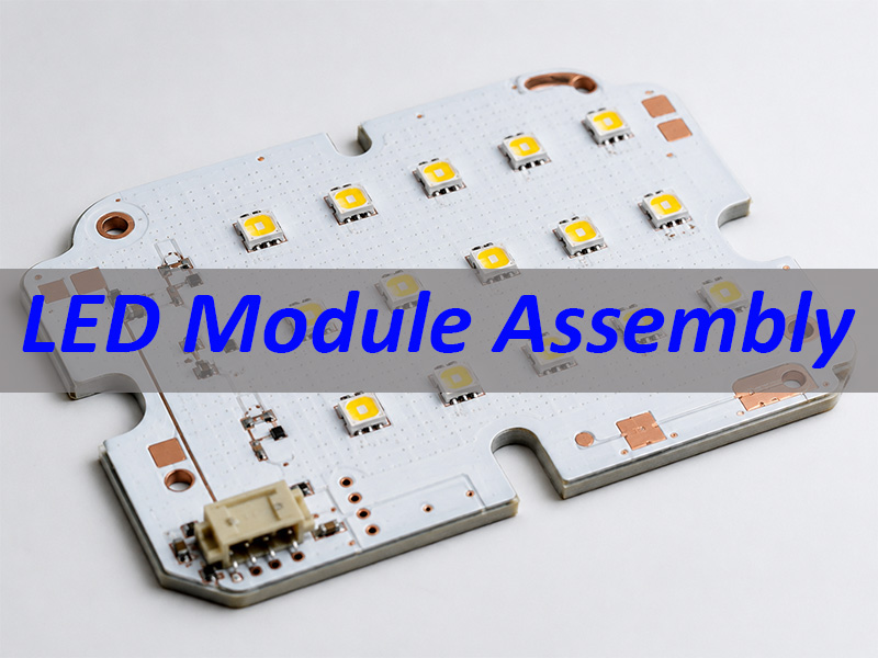
LED module assembly is not just about placing LEDs onto a PCB. A reliable lighting board needs the right PCB base, stable solder joints, correct LED polarity, controlled heat transfer, and suitable protection for the working environment.

For many lighting products, the customer already controls the final lamp housing, optics, driver, structure, and product-level validation. The PCB and PCBA partner focuses on the assembled lighting board: MCPCB fabrication, SMT LED mounting, soldering control, coating support, and basic testing.

This guide explains what buyers should know before sourcing LED module assembly for lighting boards.

LED Module Assembly

What Is LED Module Assembly?

LED module assembly is the process of turning a bare LED PCB into an assembled lighting board. It usually includes PCB fabrication, solder paste printing, SMT LED mounting, lead-free reflow soldering, inspection, testing, and sometimes protective coating.

In PCB manufacturing, an LED module does not always mean a complete finished lamp. It usually means the LED board inside the product. The housing, lens, driver, thermal structure, final packaging, and product certification may still belong to the customer’s final product scope.

This distinction matters. If you need only the bare board, you are requesting LED PCB or MCPCB fabrication. If you need LEDs mounted and tested, you are requesting LED module assembly or LED PCB assembly.

ItemLED PCBLED Module
StatusBare boardAssembled lighting board
LEDsNot mountedMounted and soldered
FunctionCannot light up aloneCan be powered and tested
Main servicePCB fabricationPCB + SMT assembly
Quality focusMaterial, copper, finishSoldering, polarity, function
LED Module Assembly

Why Are MCPCBs Used in LED Lighting Boards?

LEDs generate heat during operation. If heat stays near the LED package and solder joint, the module may face faster brightness decay, color shift, solder stress, or early failure. That is why many LED lighting boards use MCPCBs, especially aluminium core PCBs.

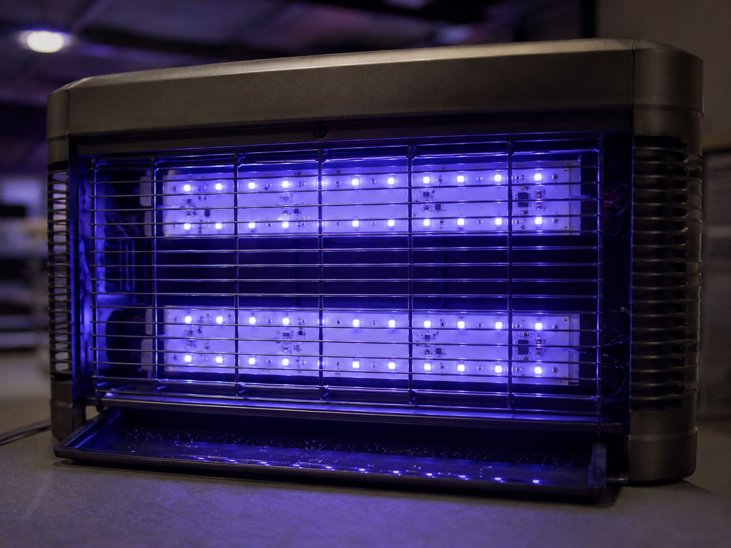
A metal-core PCB gives heat a better path from the LED pad area toward the metal base. This is especially useful for compact lighting boards, circular LED modules, UV LED boards, insect trap modules, and higher-power LED applications.

Thermal FactorFR4 ExampleIMS / MCPCB ExampleMeaning
Thermal conductivityAbout 0.25 W/m·KAbout 3 W/m·K dielectricBetter heat transfer
Junction-to-ambient thermal resistance61.56°C/W39.1°C/WLower thermal resistance
Main roleCircuit carrierCircuit carrier + heat-spreading baseMore suitable for many LED boards

This does not mean every LED board must use aluminum PCB. Low-power LED boards may still use FR4. But when heat, service life, compact space, or continuous operation matters, MCPCB is often the safer starting point.

The PCB manufacturer’s role is to build the selected board structure correctly: metal base, dielectric layer, copper thickness, solder mask, surface finish, outline, flatness, and solderability.

How Does LED Module Assembly Work?

A good LED module starts with file review. Before production, the manufacturer should check the Gerber files, BOM, pick-and-place file, LED datasheet, polarity information, coating requirement, and testing requirement.

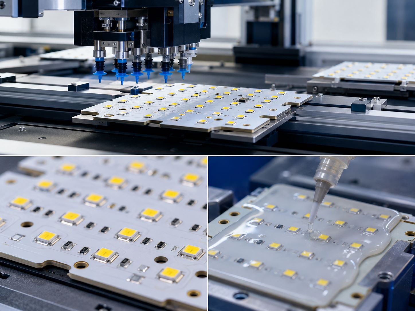
After that, the MCPCB is fabricated, LEDs are prepared, solder paste is printed, LEDs are placed by SMT equipment, and the board goes through lead-free reflow soldering. After reflow, the module is inspected, tested, and coated if required.

A practical flow looks like this:

StepWhat to Check
File reviewGerber, BOM, polarity, coating area
MCPCB fabricationMaterial, copper, finish, flatness
LED preparationPart number, bin, reel label, polarity
SMT mountingPaste volume, placement, reflow profile
InspectionVisual, AOI, polarity check
TestingElectrical and power-on test
CoatingArea, thickness, keep-out zones

The process is straightforward, but the risk is in the details. Wrong LED polarity, unstable solder paste volume, poor pad wetting, or unclear coating areas can all create defects during batch production.

What Affects LED SMT Assembly Quality?

LED SMT quality depends on PCB solderability, LED package condition, solder paste control, placement accuracy, and reflow stability.

The first key point is polarity. LEDs are directional components. If polarity is reversed, the module may not light up. Polarity should be clear in the datasheet, BOM, assembly drawing, and first article inspection.

The second key point is solder volume. Too much solder can cause LED tilt or movement. Too little solder can create weak joints. On aluminum PCBs, the metal base also affects heat absorption during reflow, so the reflow profile should be verified with the actual board when needed.

The third key point is LED bin control. For lighting boards, mixed LED bins can cause visible brightness or color differences even if every LED turns on.

RiskResultControl Point
Wrong polarityLED does not lightPolarity check
Too much solderTilt or shiftingStencil and paste control
Too little solderWeak jointPaste process control
Poor wettingUnstable solderingSurface finish and reflow
Mixed LED binsColor or brightness mismatchReel and bin traceability

For customer-supplied LEDs, the assembler should confirm reel labels, bin codes, polarity marks, storage condition, and spare quantity before production.

How Does PCB Layout Support Heat Dissipation?

PCB layout can support heat dissipation, but it does not replace full lamp thermal design. This boundary should be clear.

From the PCB and PCBA side, the focus is on manufacturable details: LED thermal pad connection, copper area, current path width, solder mask opening, pad solderability, board flatness, and MCPCB material selection.

A typical heat path in an aluminum PCB LED module is:

LED package → solder joint → copper pad → thermal dielectric layer → aluminum base → housing or air.

The PCB/PCBA manufacturer can support the first part of this path through board fabrication and SMT quality control. But final temperature still depends on the customer’s housing, heat sink, airflow, screw pressure, thermal interface, LED current, and working environment.

So the right message is not “we design the whole lamp thermal system.” The right message is: the PCB and assembly process help build a stable thermal path inside the LED lighting board.

When Is Protective Coating Needed?

Protective coating is useful when LED modules may face moisture, dust, insects, condensation, cleaning exposure, or semi-outdoor conditions. This is common in insect light traps, industrial lighting, agricultural lighting, and boards used in harsh environments.

Silicone conformal coating is often used on LED boards because it is flexible and suitable for environmental protection. But coating must be controlled carefully.

Coating TypeTypical Thickness Range
Acrylic / Epoxy / Urethane0.03–0.13 mm
Silicone0.05–0.21 mm
Parylene0.01–0.05 mm

The coating drawing should define where coating is required and where it must be avoided. Connectors, test points, screw holes, contact areas, and optical surfaces may need keep-out zones.

Poor coating control can create bubbles, uneven appearance, blocked connectors, contaminated pads, or reduced light performance. For LED modules, coating is both a protection process and a quality-control point.

LED Module Assembly

How Should LED Modules Be Tested?

Power-on testing is necessary, but it is not the whole quality check. A module can light up and still have weak solder joints, mixed LED bins, coating defects, or unstable current.

A practical LED module test plan may include:

Test ItemPurpose
Visual inspectionCheck appearance and contamination
AOICheck placement and visible solder joints
Polarity checkPrevent reversed LEDs
Electrical testCheck shorts, opens, continuity
Power-on testConfirm light-up function
Current checkConfirm operating condition
Coating inspectionCheck coverage and keep-out areas
Sample agingFind early failures before shipment

The test scope should match the application. A simple indoor board may need basic testing. A higher-reliability or semi-outdoor lighting board may need stricter inspection, current checks, coating inspection, and sample aging.

Buyers should define test voltage, current limit, inspection standard, coating acceptance criteria, and aging requirement before quotation.

What Should Buyers Prepare Before an LED Module RFQ?

A clear RFQ helps the supplier quote faster and avoid wrong assumptions. For early discussion, a rough drawing may be enough for a ballpark estimate. For formal quotation, complete engineering files are needed.

Useful RFQ documents include:

RFQ FileWhy It Matters
Gerber and drill filesPCB fabrication
BOMComponent and assembly review
Pick-and-place fileSMT programming
LED datasheetPackage, polarity, soldering data
Assembly drawingPlacement and special notes
Coating drawingCoating and keep-out control
Test requirementInspection and quotation scope
QuantityPrice and lead time

If LEDs are supplied by the customer, also provide part number, manufacturer, reel label, bin code, polarity mark, storage condition, MSL information if applicable, and spare quantity for SMT loss.

The more complete the RFQ, the easier it is to confirm feasibility, sample lead time, production cost, and quality control.

LED Module Assembly Case Study: How Does EBest Circuit Support MCPCB and SMT Projects?

A practical LED module assembly project often starts with a clear board specification. For one LED lighting board project, EBest Circuit supported a single-sided aluminum PCB with 2.0 mm finished thickness, 2 W/m·K thermal conductivity, 2 oz copper, white solder mask, black legend, and OSP surface finish.

Board RequirementSpecificationAssembly Value
PCB structureSingle-sided aluminum PCBLED board base
Finished thickness2.0 mm ±10%Board rigidity
Thermal conductivity2 W/m·KHeat transfer
Copper weight2 ozCurrent support
Solder maskWhite solder maskLight reflection
LegendBlack legendClear marking
Surface finishOSPSMT soldering

For this type of LED module assembly, the focus is not only PCB fabrication. The assembly process also needs to control LED polarity, solder paste volume, placement accuracy, and reflow soldering. If silicone conformal coating is required, the coating area and keep-out zones should be confirmed before production.

In this project type, EBest Circuit’s role is focused: manufacture the MCPCB, support SMT LED mounting, control soldering quality, and prepare the assembled lighting board for the customer’s next production step. The final lamp housing, optics, driver system, and product-level thermal validation remain part of the customer’s complete product design.

This case shows why LED module assembly should be evaluated as a combined PCB and SMT PCB manufacturing process. Board material, copper weight, surface finish, LED placement, and testing all affect the final reliability of the lighting board.

Why Choose EBest Circuit (Best Technology) for LED Module Assembly?

For LED module assembly projects, buyers need more than an SMT supplier who can simply place LEDs. A reliable LED lighting board often involves PCB fabrication, component control, SMT assembly, soldering quality, protective coating, inspection, and production traceability. When these steps are handled by separate suppliers, communication gaps and production risks can increase.

EBest Circuit (Best Technology) supports LED lighting board projects with an integrated PCB and PCBA manufacturing approach. Before production, our team can review Gerber files, BOM, pick-and-place data, LED datasheets, coating requirements, and test requirements to help customers identify potential manufacturing issues during the sample stage.

AdvantageValue for LED Module Assembly
PCB + PCBA factoriesFewer handoff risks
MCPCB and LED board experienceBetter process understanding
DFM and BOM reviewEarlier issue detection
SMT LED mountingPrototype to batch support
Consigned LED supportCustomer-specified parts
Coating and testing supportMore complete delivery
Digital traceabilityBatch and progress tracking
Quality certificationsHigher quality control needs

These advantages apply to different LED lighting board projects, including aluminum LED boards, FR4 LED boards, UV LED modules, industrial lighting boards, insect trap LED modules, customer-supplied LED assembly projects, and LED modules that require protective coating or basic function testing. The board material, copper weight, surface finish, LED package, and test requirements may vary, but the goal is the same: helping customers move from design files to controlled production.

EBest Circuit’s value is not claiming to design the complete finished lamp. Our focus is LED lighting board manufacturing: PCB fabrication, SMT LED mounting, process review, consigned material handling, coating support, inspection, and basic testing. The final lamp housing, optics, driver system, and product-level thermal validation remain part of the customer’s complete product design.

With 20 years of PCB and PCBA manufacturing experience, engineering support, quality systems, and traceable production management, EBest Circuit helps customers move LED lighting board projects from sample validation to more stable batch production.

FAQs About LED Module Assembly

What is LED module assembly?

LED module assembly is the process of fabricating an LED PCB, mounting LEDs and related components, soldering them, inspecting the board, and testing the assembled lighting board.

Is LED module assembly the same as finished lamp manufacturing?

No. LED module assembly usually focuses on the lighting board. Finished lamp manufacturing may also include housing, optics, driver integration, mechanical assembly, labeling, packaging, and product-level certification.

Why are aluminum PCBs used for LED modules?

Aluminum PCBs are used because they provide a better thermal path than standard FR4 in many LED lighting applications.

Can customer-supplied LEDs be used?

Yes. Consigned LEDs can be used if the buyer provides clear part numbers, reel labels, bin codes, polarity information, storage details, and enough spare quantity for SMT process loss.

What is silicone conformal coating used for?

Silicone conformal coating helps protect LED modules from moisture, dust, insect contamination, and environmental exposure.

What files are needed for a quote?

Gerber files, BOM, pick-and-place file, assembly drawing, LED datasheet, coating drawing, test requirements, and quantity are usually needed.

To summarize, LED module assembly is not only about mounting LEDs. A reliable lighting board depends on MCPCB material, copper layout, soldering quality, LED polarity, component traceability, protective coating, and defined testing.

For buyers, the better partner is not simply a supplier who can place LEDs. It is a PCB and PCBA manufacturer who understands how board fabrication and SMT assembly affect LED module reliability.

EBest Circuit supports LED lighting board projects with MCPCB fabrication, SMT LED mounting, consigned LED handling, conformal coating, and basic module testing. Pls feel free to send your Gerber files, BOM, pick-and-place data, LED datasheets, coating requirements, and test requirements to sales@bestpcbs.com for review.

You may also like

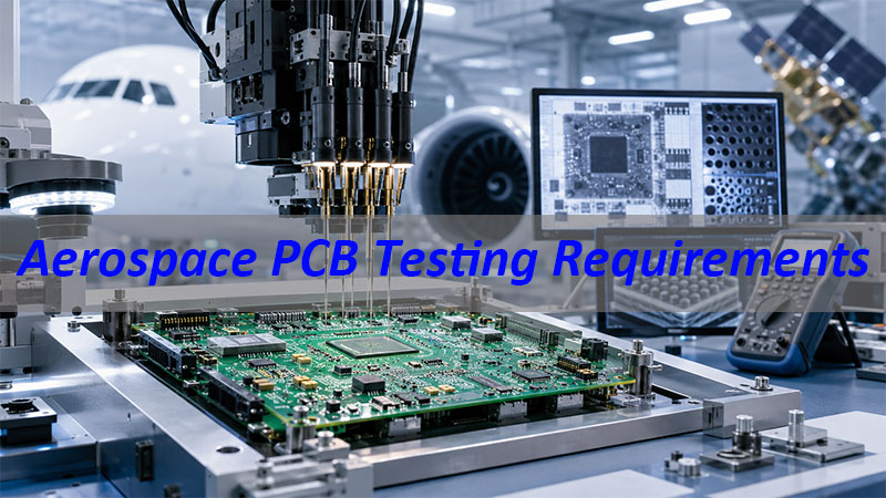
Aerospace PCB Testing Requirements: Standards, Tests and Documents

June 15th, 2026

Aerospace PCB testing requirements are the inspection, verification, documentation, and traceability rules used to confirm that an aerospace printed circuit board can meet high-reliability expectations before it is accepted for use. This article explains the key standards, bare board tests, electrical testing rules, microsection and TDR requirements, aerospace PCB assembly tests, and supplier deliverables that buyers should understand before placing an order.

For many buyers, the difficult part is not knowing that aerospace PCBs should be “high reliability.” The difficult part is turning that idea into clear purchase requirements. If the RFQ only says “IPC Class 3” or “aerospace quality,” suppliers may quote differently, test differently, and deliver different levels of evidence.

Common problems usually start like this:

  • The supplier says “Class 3,” but the required standard stack is not clear.
  • The buyer asks for testing, but does not define 100% test or sampling.
  • Microsection, impedance, and X-ray requirements are discussed too late.
  • The PCBA supplier and bare board factory treat responsibilities differently.
  • The buyer receives only a CoC, with limited test data or traceability.
  • Environmental testing is assumed, but no one defines who owns it.
  • A material or process change happens without proper approval.

A better approach is to define aerospace PCB testing requirements as a complete acceptance package. It should include applicable standards, required tests, sampling rules, deliverable documents, traceability depth, change control, and nonconformance handling.

Aerospace PCB Testing Requirements

What Are Aerospace PCB Testing Requirements?

Aerospace PCB testing requirements are the rules used to verify whether a PCB is acceptable for aerospace, aviation, space, or defense-related electronics. They cover more than one test. They include design review, material verification, bare board inspection, electrical testing, assembly inspection, functional testing, environmental validation, and documentation.

In practical sourcing, aerospace PCB testing requirements usually answer these questions:

  • Which standards apply?
  • What class level is required?
  • What tests are mandatory?
  • Which tests can be risk-based?
  • Is electrical testing 100% or sampling?
  • Are microsection and impedance reports required?
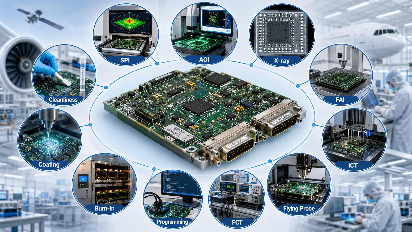
  • Does the project need PCBA testing or system-level validation?
  • What documents must the supplier deliver?
  • How deep should traceability go?
  • What happens if a nonconformance is found?

This matters because aerospace PCBs are often used in products where failure is expensive, difficult to repair, or safety-related. These boards may work in vibration, thermal cycling, altitude change, humidity, long service life, and strict maintenance environments.

Aerospace PCB testing requirements should be clear enough that a supplier can quote, manufacture, test, document, and ship the product without guessing. If a requirement is important, it should be written into the RFQ, drawing notes, purchase order, inspection plan, or quality agreement.

A useful principle is simple: do not ask only for “aerospace quality.” Ask for measurable standards, test methods, report formats, and acceptance rules.

Why Do Aerospace PCBs Need Stricter Testing?

Aerospace PCBs need stricter testing because their working environment is more demanding than many commercial electronic products. A standard PCB may pass basic manufacturing inspection, but that does not automatically make it suitable for aerospace PCB applications.

Aerospace and defense PCB assemblies may face:

  • Wide temperature changes
  • Thermal cycling and thermal stress
  • Vibration and mechanical shock
  • Humidity and contamination risk
  • High altitude or low-pressure conditions
  • Long operating life
  • Dense routing and controlled impedance
  • High current or high-frequency signals
  • Limited repair access after installation
  • Strict audit and documentation requirements

The risk is not always visible. A board can look good on the surface but still have hidden defects such as weak hole-wall plating, microvia cracks, resin voids, poor solder joints, insufficient annular ring, poor impedance control, or unverified material substitution.

For buyers, the key point is this: aerospace PCB testing is not only about finding defects. It is about proving that the board was built, inspected, and documented under controlled conditions.

That is why aerospace printed circuit boards often require more than a final electrical pass. They may need material certificates, process records, cross-section data, impedance coupon results, X-ray evidence, first article inspection, and controlled change records.

A high reliability PCB for aerospace is not defined by one inspection step. It is defined by the full control chain from material selection to final test report.

Which Standards Apply to Aerospace PCBs?

Several standards may apply to aerospace PCBs, depending on whether the project is a bare board, an assembled PCBA, a space-grade board, a defense program, or part of certified airborne electronic hardware.

The buyer should avoid writing one vague sentence such as “must meet aerospace standards.” Instead, the required standards should be separated by scope.

Common standard areas include:

ScopeCommonly Used Standard or Requirement
Bare rigid PCB performanceIPC-6012, project class requirement
Space or military avionics rigid PCBIPC-6012ES / IPC-6012FS if required
Bare board visual acceptabilityIPC-A-600
PCBA workmanshipIPC-A-610 Class 3
Soldering processJ-STD-001 Class 3
Aerospace quality systemAS9100D
First article inspectionAS9102 when required
Environmental qualificationDO-160, MIL-STD-810, or project test plan
Military QML programMIL-PRF-31032 when required
Airborne electronic hardware evidenceDO-254 / AC 20-152A context when applicable

Not every aerospace PCB project needs every standard. A ground support device, an aircraft cabin control board, a UAV power module, a space-grade PCB, and a defense radar assembly may have different requirements.

For buyers, the practical rule is:

  • Use IPC standards to define PCB and PCBA workmanship and acceptance.
  • Use AS9100D to evaluate the supplier’s aerospace quality management system.
  • Use AS9102 if first article inspection documentation is required.
  • Use DO-160 or MIL-STD-810 when environmental qualification is required.
  • Use MIL-PRF-31032 only when the program or customer specification requires that military QML framework.
  • Use DO-254 / AC 20-152A when the PCB or PCBA evidence must support airborne electronic hardware certification and configuration control.

DO-254 and AC 20-152A are not normal PCB fabrication standards. They become relevant when the board-level manufacturing evidence supports hardware verification, configuration baseline, and certification records for airborne systems.

A clear standard stack reduces confusion. It also helps suppliers quote correctly instead of assuming a lower test or documentation level.

IPC Class 3, Class 3A or IPC-6012ES?

IPC Class 3, Class 3A, and IPC-6012ES are often discussed together, but they are not the same thing. Buyers should not treat them as interchangeable labels.

A simple way to understand them is:

  • IPC Class 3
    Used for high-performance electronic products where continued performance or performance-on-demand is critical.
  • IPC Class 3A / Class 3/A
    Used when the customer or project requires a higher avionics or mission-critical expectation beyond normal Class 3 wording. It should be clearly defined by the applicable IPC document and procurement specification.
  • IPC-6012ES / IPC-6012FS
    Addendum requirements for rigid printed boards used in space and military avionics applications. These add requirements or exceptions beyond normal IPC-6012 Class 3 requirements.
  • MIL-PRF-31032
    A military performance specification tied to qualified printed board manufacturing programs when the contract requires it.

For a buyer, the safest wording is not “Class 3 only.” A better requirement should define:

  • The IPC standard revision
  • The product class
  • Any applicable addendum
  • Required tests
  • Required reports
  • Sampling or 100% inspection rules
  • Traceability and change control
  • Customer approval for deviations

A simple example of clearer wording is:

“Bare printed boards shall be manufactured and inspected to IPC-6012 Class 3 and IPC-A-600 Class 3, unless otherwise specified on the drawing. If the program requires space or military avionics requirements, IPC-6012ES or the applicable current addendum shall apply. Electrical testing, microsection, impedance verification, and deliverable reports shall follow the approved inspection plan.”

This wording is only a template. The final version should match the customer drawing, contract, program specification, and regulatory context.

The main point is simple: IPC Class 3 is often a starting point, not a complete aerospace PCB testing requirement by itself.

What Tests Are Required for Bare Boards?

Bare board testing focuses on the printed circuit board before component assembly. This is where the supplier verifies that the aerospace printed circuit board was fabricated correctly.

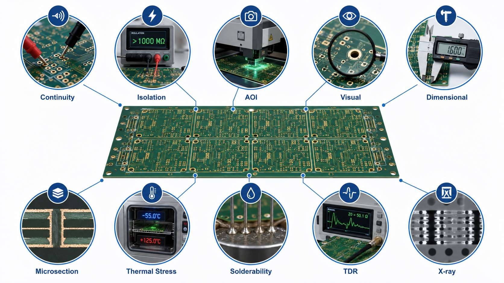
Common bare board tests include:

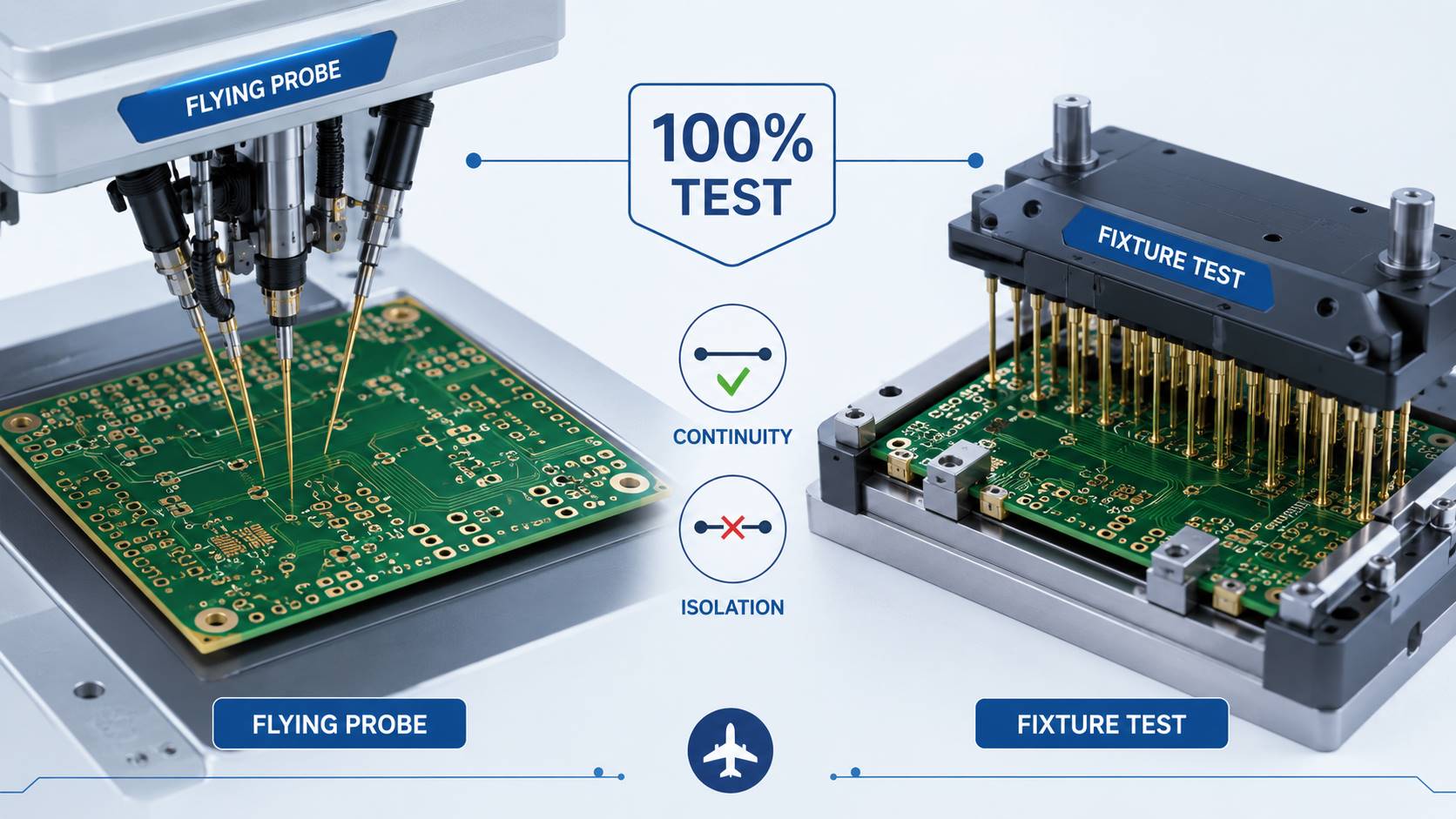
  • Continuity test
    Confirms that connected nets are electrically continuous.
  • Isolation test
    Confirms that separated nets are not shorted.
  • AOI inspection
    Checks opens, shorts, trace defects, annular ring issues, etching defects, and pattern errors.
  • Visual inspection
    Reviews solder mask, surface finish, legend, edge quality, holes, scratches, contamination, and workmanship.
  • Dimensional inspection
    Confirms board outline, hole size, slot size, thickness, registration, and critical tolerances.
  • Microsection inspection
    Checks plated-through holes, via structure, copper thickness, lamination quality, resin recession, cracks, and voids.
  • Thermal stress test
    Evaluates how plated holes and laminate structures survive soldering-related thermal stress.
  • Solderability test
    Confirms that the surface finish can accept solder properly.
  • Impedance test
    Uses coupons and TDR data to verify controlled impedance traces.
  • X-ray inspection
    May be used for hidden structures such as blind vias, buried vias, HDI features, or internal alignment concerns.

For aerospace PCBs, the key question is not only “Can you test it?” The better question is:

“How will each test be performed, recorded, sampled, and delivered?”

For example, continuity and isolation may need 100% testing. Microsection may be performed by lot or coupon. Impedance may be verified through coupon testing. X-ray may be defined for specific hidden structures or high-risk areas.

If the inspection plan is not defined before production, the buyer may receive a board that technically passed the supplier’s internal process but does not meet the buyer’s acceptance expectations.

Aerospace PCB Testing Requirements

Is 100% Electrical Testing Required?

For aerospace PCBs, 100% electrical testing is commonly expected for bare board continuity and isolation. This is because an open or short circuit can create immediate functional failure, and sampling only a few boards may miss a critical defect.

Electrical testing usually checks:

  • Net continuity
  • Net isolation
  • Opens
  • Shorts
  • Incorrect connections
  • High-resistance defects when detectable by the test method

Both flying probe and fixture-based testing can be used. The correct method depends on volume, board complexity, lead time, cost, and test coverage.

A simple comparison is:

Test MethodBest ForBuyer Concern
Flying probePrototype, small batch, complex low-volume boardsSlower for high volume
Bed-of-nails fixtureMedium to high volumeFixture cost and setup time
Universal grid / fixture testRepeat productionCoverage and fixture control

The important point is not whether the supplier uses flying probe or bed-of-nails. The important point is whether the test covers the required netlist and whether every production board is tested when required.

Buyers should avoid vague wording such as:

“Supplier shall perform electrical test.”

A stronger requirement is:

“Supplier shall perform 100% netlist-based electrical testing for continuity and isolation on all delivered bare boards. Test records shall be retained and made available upon request. Sampling-only electrical testing is not acceptable unless approved in writing.”

This is the kind of wording that prevents later disputes.

For aerospace PCB assembly, electrical testing becomes broader. It may include ICT, flying probe assembly test, functional test, programming, boundary scan, or system-level test depending on the product.

Aerospace PCB Testing Requirements

When Are Microsection and TDR Tests Needed?

Microsection and TDR tests are needed when hidden manufacturing quality or controlled impedance must be verified. These tests are especially important for high reliability PCB for aerospace projects because many critical defects are not visible from the surface.

Microsection Testing

Microsection, also called cross-section analysis, cuts through a board or coupon to inspect internal structures under magnification.

It can verify:

  • Hole-wall copper thickness
  • Plating quality
  • Barrel cracks
  • Via fill quality
  • Lamination defects
  • Resin voids
  • Inner layer registration
  • Copper wrap
  • Interconnect integrity
  • Microvia structure

Microsection is usually not performed on every production board because it is destructive. Instead, it is commonly performed on test coupons, production panels, selected samples, first article lots, or lots defined by the inspection plan.

Buyers should define:

  • When microsection is required
  • Which coupon or sample is used
  • What features must be measured
  • What photos must be delivered
  • What acceptance criteria applies
  • What happens if the result fails

TDR and Impedance Testing

TDR testing is used to verify controlled impedance. It is common for aerospace printed circuit boards used in high-speed digital, RF, radar, communication, sensor, avionics, or defense electronics.

TDR testing can confirm:

  • Single-ended impedance
  • Differential impedance
  • Coupon performance
  • Stack-up consistency
  • Transmission line control

A useful requirement may say:

“Controlled impedance shall be verified by TDR test on approved impedance coupons. Test data shall include target impedance, measured impedance, tolerance, coupon ID, lot number, and test date.”

TDR is not needed for every aerospace PCB. It is needed when the design includes controlled impedance requirements. If the drawing calls out 50Ω, 90Ω, 100Ω differential, or other controlled impedance values, the inspection plan should define how those values are verified.

In short, microsection proves hidden manufacturing quality. TDR proves controlled impedance performance. Both should be planned before production, not requested after boards are finished.

What Tests Apply to Aerospace PCB Assembly?

Aerospace PCB assembly testing applies after components are mounted. It is different from bare board testing. A PCB can pass fabrication inspection but still fail after soldering, cleaning, coating, programming, or functional operation.

Common aerospace PCB assembly tests and inspections include:

  • SPI
    Checks solder paste volume, area, height, and alignment before reflow.
  • AOI
    Checks component presence, polarity, solder joints, tombstoning, bridges, missing parts, and placement issues.
  • X-ray inspection
    Used for BGA, QFN, bottom-terminated components, hidden joints, voids, and some high-reliability solder joints.
  • First article inspection
    Confirms that the first assembled unit matches the approved BOM, drawing, placement, polarity, and workmanship requirements.
  • ICT
    Checks assembled circuit electrical characteristics when test access is available.
  • Flying probe assembly test
    Useful for low-volume or prototype aerospace PCB assembly where fixtures are not practical.
  • Functional test
    Confirms that the PCBA performs the required electrical functions.
  • Programming and firmware verification
    Applies when the assembly includes programmable devices.
  • Burn-in or aging test
    May be used to screen early failures in selected projects.
  • Conformal coating inspection
    Checks coverage, thickness, bubbles, masking, and contamination risk when coating is required.
  • Cleanliness or contamination testing
    May be required for high-reliability or sensitive assemblies.

Aerospace & defense PCB assemblies often require tighter control of BOM, component sourcing, soldering profile, rework limits, operator training, and process records.

The buyer should define whether the supplier is responsible only for PCB manufacturing, or for full PCB assembly and manufacturing for defense and aerospace applications. This boundary changes the test plan, price, lead time, and deliverable documents.

For PCBA projects, “tested” should not be a general word. It should mean a defined test flow with clear acceptance criteria.

Aerospace PCB Testing Requirements

What Documents Should Suppliers Provide?

Documentation is what closes the loop in aerospace PCB testing requirements. Without documents, the buyer may know that the boards passed, but not how, when, by whom, under which lot, and against which acceptance rule.

A proper aerospace PCB delivery package may include:

  • Certificate of Conformance
  • Material certificates
  • Laminate, prepreg, copper, solder mask, and surface finish batch records
  • Surface finish certificate if required
  • Electrical test report
  • AOI inspection summary
  • Dimensional inspection report
  • Microsection photos and measured values
  • Thermal stress or solderability test record
  • Impedance coupon and TDR report
  • X-ray report if applicable
  • PCBA inspection report
  • ICT or FCT report if applicable
  • First Article Inspection report when required
  • NCR record if any nonconformance occurred
  • CAPA or SCAR response if required
  • Approved deviation or concession record if any
  • Change notification record
  • Lot traceability or board serial number traceability
  • Packing and handling records if specified

A stamped CoC alone is not enough for many aerospace PCB projects. It may be part of the package, but it does not replace test data, material traceability, or inspection evidence.

Buyers should decide the required traceability depth before ordering.

Common traceability levels include:

  • Lot-level traceability
    Links boards to a production lot and material batch records.
  • Panel-level traceability
    Links a panel or production set to process records.
  • Board-level serial traceability
    Links each delivered board or assembly to inspection, test, and production records.

Board-level traceability costs more, but it may be necessary for mission-critical or defense-related projects.

Change control is also important. The supplier should not change laminate, prepreg, copper foil, solder mask, surface finish, approved process, outside process, or critical component substitution without approval when the project requires controlled configuration.

A good document package protects both sides. It helps the buyer pass internal review, supplier audit, incoming inspection, and failure analysis if a field issue occurs.

FAQs About Aerospace PCB Testing Requirements

Are IPC Class 3 Requirements Enough for Aerospace PCBs?

IPC Class 3 is often a starting point, but it may not be enough by itself. Aerospace PCB projects may also require IPC-6012 addendums, AS9100D quality controls, first article inspection, traceability, environmental testing, and project-specific acceptance rules.

What Is the Difference Between IPC Class 3 and Class 3A?

IPC Class 3 is used for high-performance electronic products. Class 3A, often written in some contexts as Class 3/A, is associated with higher-reliability avionics or mission-critical expectations when specified by the applicable procurement document or IPC requirement. Buyers should not use the term casually. It should be tied to the correct standard and contract requirement.

Is IPC-6012ES Required for All Aerospace PCBs?

No. IPC-6012ES is not automatically required for every aerospace PCB. It is used when the program, drawing, contract, or customer specification requires space or military avionics addendum requirements. For many aerospace electronics, IPC Class 3 with additional project-specific testing may be used instead.

Does AS9100D Certify the PCB Itself?

No. AS9100D is a quality management system standard for aerospace organizations. It does not automatically certify that every PCB meets a specific technical requirement. Buyers still need to define the PCB standard, test plan, inspection reports, and acceptance criteria.

Should Aerospace PCBs Be 100% Electrically Tested?

For bare boards, 100% continuity and isolation testing is commonly expected for aerospace PCB projects. Sampling-only testing should not be used for critical electrical acceptance unless the buyer has formally approved it.

Is Flying Probe Testing Acceptable for Aerospace PCBs?

Flying probe testing can be acceptable when it provides the required netlist coverage and documented test results. The issue is not the machine type alone. The buyer should confirm test coverage, test limits, records, and whether every delivered board is tested.

When Is Microsection Required?

Microsection is needed when plated holes, vias, lamination quality, copper thickness, or hidden structures must be verified. It is commonly performed on coupons, production panels, first articles, or lots defined by the inspection plan.

When Is TDR Testing Required?

TDR testing is required when the PCB has controlled impedance requirements. It verifies that impedance coupons meet the target values and tolerances defined by the design.

Are Environmental Tests Part of PCB Testing?

Sometimes, but not always. Bare board factories usually handle fabrication-level tests. Environmental tests such as thermal cycling, vibration, shock, humidity, altitude, or DO-160 testing are often PCBA-level, box-level, or system-level requirements. Responsibility and cost should be defined in the RFQ or test plan.

What Documents Should I Request From an Aerospace PCB Supplier?

At minimum, request CoC, material certificates, electrical test evidence, inspection records, and traceability information. For high-reliability projects, also request microsection data, impedance reports, X-ray reports, FAI records, NCR/CAPA records, and change-control documentation when applicable.

How Can I Verify an AS9100 Certificate?

Buyers should verify AS9100 certification through the IAQG OASIS database instead of relying only on a PDF certificate sent by email. The certificate scope, site address, expiration date, and certification body should match the supplier being used.

Why Do Aerospace PCB Testing and Documentation Increase Cost?

The cost is higher because the supplier must perform more verification, maintain traceability, control materials, prepare records, manage audits, and sometimes support first article inspection or special process controls. The extra cost is mainly risk control, not only board fabrication.

To wrap up, Aerospace PCB testing requirements define the standards, inspections, test reports, traceability, and acceptance rules needed before aerospace printed circuit boards enter high-reliability applications.

For buyers, the key is to define the required tests clearly, including bare board electrical testing, microsection, impedance verification, aerospace PCB assembly inspection, and supplier documentation.

If you need aerospace PCB manufacturing, PCBA assembly, or DFM review, please feel free to send your Gerber files, BOM, stack-up, and project requirements to EBest Circuit (Best Technology) at sales@bestpcbs.com. As one of the experienced aerospace PCB manufacturers, we can help you review technical requirements, testing expectations, and production feasibility before manufacturing starts.

You may also like

Aerospace PCB Manufacturer

June 15th, 2026

Aerospace PCB are built for environments where reliability matters from the first design review to final field operation. A circuit board used in aviation, satellite communication, radar, navigation, UAV control, aerospace testing equipment, or other mission-critical systems cannot be treated like a standard commercial PCB. It requires stable materials, controlled processes, strict inspection, and clear documentation.

Aerospace PCB Manufacturer

That is why choosing the right aerospace PCB manufacturer is not only a purchasing decision. It is also a risk-control decision.

At EBest Circuit, we support aerospace-related PCB projects that require high reliability, engineering communication, controlled materials, precision manufacturing, and PCB assembly support. Our capabilities include high-Tg PCB, HDI PCB, rigid-flex PCB, RF PCB, heavy copper PCB, metal core PCB, ceramic PCB, multilayer PCB, and PCBA services. From prototype verification to small-batch production and repeat orders, our engineering and manufacturing teams help customers turn demanding designs into reliable circuit boards.

Why Aerospace PCB Projects Need More Than Standard PCB Manufacturing?

An aerospace PCB is a printed circuit board designed for aerospace-related electronic systems. These systems may be used in aircraft, satellites, avionics, radar modules, navigation equipment, unmanned aerial vehicles, defense electronics, power control units, sensors, and ground support equipment.

The difference between an aerospace PCB and a standard PCB is not only the application name. The real difference lies in reliability requirements, material selection, process control, testing, and traceability.

A standard commercial PCB may mainly focus on cost, basic function, and delivery time. Aerospace PCB projects usually require more attention to thermal stability, vibration resistance, signal integrity, mechanical strength, long-term operation, and production consistency. In many cases, failure can be expensive, difficult to repair, or unacceptable.

This is why aerospace PCB manufacturing requires more than a low-cost PCB supplier. It needs a manufacturer that understands engineering risk, manufacturing tolerance, inspection discipline, and documentation control.

For customers, the key question is not simply, “Can you make this board?” A better question is, “Can you help us make this board stable, repeatable, and suitable for a high-reliability application?”

That is the value we aim to provide.

What Makes Aerospace PCBs Difficult to Manufacture?

Aerospace PCB projects are challenging because the working environment is often harsher than that of common industrial or consumer electronics. The board may need to handle temperature changes, vibration, shock, high-frequency signals, dense layouts, power loads, or limited installation space.

Aerospace PCB Manufacturer

Several design and manufacturing factors can directly affect reliability.

  • Temperature cycling can create stress between copper, dielectric materials, solder joints, vias, and component pads. If the material is not selected properly, the board may face expansion mismatch, delamination risk, or unstable electrical performance.
  • Vibration and mechanical shock can affect solder joints, connectors, plated through holes, and flexible sections. For aircraft, UAVs, and aerospace control systems, mechanical reliability is a serious concern.
  • High-frequency communication and radar systems require controlled impedance, stable dielectric properties, smooth signal paths, and careful stack-up design. Even a small material or process variation may affect signal performance.
  • Power control and high-current modules need proper copper thickness, thermal path design, and sometimes heavy copper, metal core, or ceramic substrate solutions. Poor thermal design can reduce long-term reliability.
  • Space-constrained aerospace electronics may require HDI PCB or rigid-flex PCB. These boards need tighter control over drilling, plating, lamination, registration, flex bending areas, and stack-up balance.
  • Documentation is also important. Aerospace-related projects often require controlled material records, production traceability, inspection reports, test data, and clear communication during engineering review.

Because of these factors, aerospace PCB projects should be handled through a controlled manufacturing process, not a simple quote-and-build workflow.

Our Aerospace PCB Manufacturing Capabilities

EBest Circuit supports aerospace-related PCB projects with a wide range of PCB technologies. This helps customers choose the right board structure according to the application, reliability target, space limitation, thermal requirement, signal speed, and assembly needs.

Our PCB manufacturing capabilities include:

  • High-Tg PCB for applications that require better thermal stability than standard FR4
  • Multilayer PCB for complex aerospace control and communication systems
  • HDI PCB for compact and high-density electronic designs
  • Rigid-flex PCB for space-limited and vibration-sensitive equipment
  • RF and high-frequency PCB for radar, antenna, communication, and microwave-related modules
  • Heavy copper PCB for power control, current-carrying circuits, and high-load applications
  • Metal core PCB for improved heat dissipation in power and lighting modules
  • Ceramic PCB for high thermal conductivity, dimensional stability, and demanding power applications
  • PCBA service for customers who need PCB fabrication, component sourcing, SMT assembly, testing, and box-build support

This broad technology coverage allows us to support different aerospace electronic projects instead of being limited to one board type.

For example, an avionics control module may need a high-Tg multilayer PCB. A radar module may require RF laminate and impedance control. A compact UAV control board may need HDI or rigid-flex technology. A high-power aerospace lighting or power module may need metal core PCB, heavy copper PCB, or ceramic PCB. Different systems require different solutions.

Our role is to help customers evaluate the design, material, structure, and manufacturing route before production starts.

What Types of PCBs Can Be Used in Aerospace Electronics?

Aerospace electronics may use many types of circuit boards. The right choice depends on the operating environment, electrical function, mechanical layout, and reliability requirements.

Rigid PCBs are widely used in control modules, power circuits, communication equipment, test systems, and many aerospace-related electronic products. They can be made as single-layer, double-layer, or multilayer boards. For higher reliability, high-Tg materials, controlled stack-up, stable copper thickness, and stricter inspection are often required.

Many aerospace systems need multilayer PCBs because the circuit design may include power planes, ground planes, high-speed signals, control signals, and shielding layers. A stable multilayer stack-up helps improve signal integrity, EMC performance, and routing density.

HDI PCB is useful when aerospace electronics need smaller size, lighter weight, and higher component density. Microvias, blind vias, buried vias, and fine lines can help reduce board area while supporting complex routing. HDI manufacturing requires accurate drilling, plating, lamination, and registration control.

Rigid-flex PCB is valuable in aerospace electronics because it can reduce connectors, save space, and improve mechanical reliability in compact assemblies. Instead of using multiple rigid boards connected by cables, a rigid-flex structure can integrate rigid sections and flexible interconnection areas into one board.

This is especially useful for avionics modules, UAV electronics, sensor assemblies, compact control units, and devices exposed to vibration.

Radar, antenna, satellite communication, and aerospace RF modules may require PTFE or other high-frequency laminates. These materials support more stable signal performance at higher frequencies. The PCB manufacturer must control impedance, dielectric thickness, copper profile, routing geometry, and surface finish.

Heavy copper PCB is used when the circuit needs to carry higher current or manage stronger power loads. Aerospace power control units, power distribution boards, motor control systems, and high-current modules may use thicker copper to improve current capacity and thermal performance.

Metal core PCBs, especially aluminum or copper base boards, help transfer heat away from power devices. They can be used in aerospace lighting, power modules, LED systems, and thermal management applications.

Aerospace PCB Manufacturer

Ceramic PCB can support high thermal conductivity, good dimensional stability, and strong electrical insulation. It is suitable for high-power, high-temperature, and compact electronic modules. Aerospace-related power electronics, sensor modules, laser systems, and high-reliability thermal designs may benefit from ceramic substrates.

Materials We Support for Aerospace PCB Applications

Material selection is one of the most important decisions in aerospace PCB manufacturing. A material that works well in a simple commercial product may not be suitable for high-reliability aerospace electronics.

We support several material options for aerospace-related PCB projects.

High-Tg FR4 is often used when the PCB needs better thermal resistance and dimensional stability than standard FR4. It is suitable for multilayer PCBs, control boards, communication boards, and industrial-grade aerospace-related electronics.

Polyimide is commonly used in flexible PCB and rigid-flex PCB. It offers good flexibility and thermal resistance, making it suitable for compact, bendable, and vibration-sensitive electronic assemblies.

PTFE and other RF materials are used in high-frequency applications such as radar, antenna, satellite communication, and microwave modules. These materials help maintain more stable dielectric performance at high frequencies.

Heavy copper is selected for high-current and power control circuits. It improves current-carrying capability and can also help with heat spreading in power sections.

Metal core materials help dissipate heat from power components. Aluminum base PCB is widely used in thermal management applications, while copper base PCB can offer stronger heat transfer for more demanding designs.

Ceramic materials such as alumina and aluminum nitride can be used when the design needs high thermal conductivity, electrical insulation, and dimensional stability. Ceramic PCB is especially useful for compact power electronics and high-heat applications.

Instead of recommending one material for every project, we help customers evaluate material options based on real operating conditions. These include working temperature, current load, signal frequency, board size, component density, mechanical stress, and testing requirements.

Engineering Support Before Aerospace PCB Production

For aerospace PCB projects, engineering review before manufacturing is extremely important. A design may look complete in Gerber files, but small details can still affect yield, cost, delivery, or long-term reliability.

Our engineering team can support customers with practical design and manufacturability reviews before production.

This review may include:

  • Gerber file checking
  • Stack-up review
  • Material suggestions
  • Copper thickness review
  • Drill size and via structure review
  • Impedance control review
  • Minimum line width and spacing check
  • Annular ring and drill-to-copper clearance review
  • Solder mask bridge and pad design review
  • Surface finish recommendation
  • Thermal path review
  • Assembly feasibility review
  • Panelization suggestion
  • Special inspection and documentation review

This step helps customers identify potential manufacturing risks before the board enters production. It can also reduce unnecessary redesign, production delays, and quality uncertainty.

Aerospace PCB Manufacturer

For example, if an aerospace-related board has high-current areas, we may review whether the copper thickness, trace width, via quantity, and thermal path are suitable. If the board includes RF sections, we may check impedance requirements and material compatibility. If the project uses rigid-flex PCB, we may review bend areas, coverlay openings, stiffener design, and stack-up transitions.

Quality Control for Aerospace PCB Manufacturing

Quality control for aerospace PCB manufacturing does not begin at final inspection. It starts before production and continues through every key process.

For high-reliability PCB projects, a stable process is more important than simply checking the finished board. Material selection, stack-up confirmation, inner layer inspection, lamination, drilling, plating, solder mask, surface finish, electrical testing, and final packaging all affect the final result.

Our quality control process can include:

  • Incoming material inspection
  • Engineering file review
  • Stack-up confirmation
  • Inner layer AOI
  • Lamination process control
  • Drilling inspection
  • Plating thickness control
  • Solder mask inspection
  • Surface finish inspection
  • Electrical testing
  • Impedance testing when required
  • Microsection analysis when required
  • Final visual inspection
  • Packing inspection
  • Traceability documentation

For PCBA projects, additional quality control can include:

  • BOM review
  • Component sourcing control
  • Solder paste inspection
  • SMT placement inspection
  • Reflow process control
  • AOI inspection
  • X-ray inspection for BGA or hidden solder joints
  • DIP inspection
  • Functional testing when required
  • Conformal coating when required
  • Final assembly inspection

For aerospace-related electronics, customers often need more than a good-looking PCB. They need confidence that the board is built through a controlled and repeatable process.

If your project requires specific inspection reports, material traceability, test records, or customer-defined acceptance standards, our team can review these requirements before quotation and production.

Quality Systems and Manufacturing Discipline

Aerospace PCB projects often require strong quality management. Customers may need suppliers that understand structured documentation, process control, traceability, corrective action, and consistent production management.

EBest Circuit has long-term experience supporting high-reliability PCB and PCBA projects across industrial control, automotive electronics, medical devices, communication equipment, power electronics, and aerospace-related applications.

Our quality system support covers project requirements related to ISO9001, ISO13485, IATF16949, and AS9100D. These systems help strengthen manufacturing discipline, supplier control, documentation awareness, production consistency, and risk management.

For customers, this matters because aerospace PCB projects are not only about manufacturing capability. They are also about communication quality, process discipline, and the ability to handle engineering details carefully.

A capable aerospace PCB manufacturer should be able to discuss technical questions clearly, review project risks, follow controlled procedures, and provide useful feedback before and during production.

That is the type of support we aim to deliver.

PCB Assembly Support for Aerospace-Related Electronics

Many aerospace customers do not only need bare PCB fabrication. They also need PCB assembly, component sourcing, testing, coating, or box-build support.

We provide PCBA services to help customers reduce supply chain complexity and improve project communication. Instead of managing separate suppliers for PCB fabrication, component sourcing, assembly, testing, and final packaging, customers can work with one team for a more integrated process.

Our PCBA capabilities include:

  • SMT assembly
  • DIP assembly
  • Fine-pitch component assembly
  • BGA assembly
  • QFN and QFP assembly
  • Component sourcing support
  • BOM review
  • PCB fabrication and assembly coordination
  • SPI inspection
  • AOI inspection
  • X-ray inspection
  • Functional testing
  • Conformal coating
  • Box-build assembly

This one-stop support is especially valuable for engineering teams that need prototype builds, design verification, small-batch production, or stable repeat orders.

For aerospace-related projects, assembly quality can be just as important as PCB fabrication quality. Solder joint reliability, component placement, thermal profile control, cleaning, inspection, and functional testing all affect final performance.

By combining PCB manufacturing and PCBA support, we help customers reduce handover risks between suppliers and improve communication efficiency.

From Aerospace PCB Prototype to Batch Production

Aerospace-related electronics often start with engineering samples or small-batch verification. The design may need several rounds of testing before it enters stable production.

We support customers through different project stages:

  • Engineering prototype
  • Design verification build
  • Small-batch production
  • Pilot run
  • Batch production
  • Repeat order manufacturing
  • PCB assembly and testing
  • Box-build support when required

For prototype projects, speed and engineering feedback are important. Customers need to know whether the design can be manufactured, whether the material is suitable, whether the stack-up is practical, and whether special testing is needed.

For batch production, consistency becomes more important. Customers need stable material supply, repeatable manufacturing processes, controlled inspection, and clear documentation.

Because we support both prototype and production stages, customers can move from early design review to later production with better continuity.

This is especially useful for aerospace-related projects where design knowledge, manufacturing history, and quality records should remain consistent across development stages.

What Files Should You Send for an Aerospace PCB Quote?

A complete quotation package helps the engineering team evaluate your aerospace PCB project faster and more accurately.

For bare PCB fabrication, please prepare:

  • Gerber files
  • Drill files
  • Stack-up requirement
  • Board thickness
  • Material requirement
  • Copper thickness
  • Surface finish
  • Solder mask color
  • Silkscreen requirement
  • Controlled impedance requirement
  • Minimum line width and spacing
  • Special tolerance requirement
  • IPC class or customer acceptance standard
  • Testing requirement
  • Quantity
  • Expected lead time

For PCBA projects, please also provide:

  • BOM
  • CPL or pick-and-place file
  • Assembly drawing
  • Testing procedure if available
  • Programming requirement if needed
  • Functional test requirement
  • Conformal coating requirement if needed
  • Box-build documents if required

If you are not sure whether your files are complete, you can send the available files first. Our engineering team can help check what is missing and provide feedback before production.

Why Choose EBest Circuit for Aerospace PCB Projects?

Choosing an aerospace PCB manufacturer is about more than price. A lower quotation may not reduce project risk if the supplier cannot support engineering review, material control, reliable manufacturing, inspection, and documentation.

EBest Circuit is positioned to support demanding aerospace-related PCB and PCBA projects through manufacturing experience, broad technology coverage, engineering communication, and one-stop service.

Founded in 2006, EBest Circuit has long-term experience in PCB manufacturing and PCB assembly. We serve customers in industrial control, automotive electronics, medical devices, communication systems, power electronics, aerospace-related electronics, and other high-reliability fields.

This experience helps us understand that different industries care about different risks. For aerospace-related projects, we pay close attention to reliability, materials, thermal performance, signal quality, inspection, and traceability.
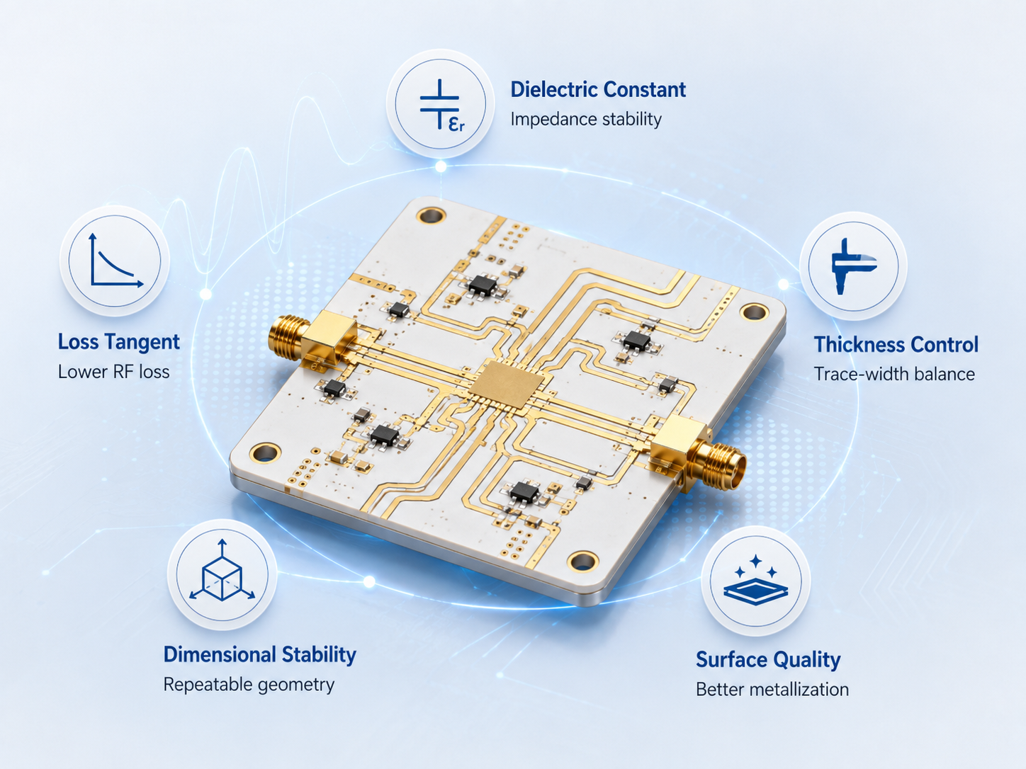
We are not limited to one PCB type. Our capabilities include high-Tg PCB, HDI PCB, rigid-flex PCB, RF PCB, heavy copper PCB, metal core PCB, ceramic PCB, multilayer PCB, and PCBA.

This gives customers more flexibility when choosing the right solution for their aerospace electronic products.

We do not only quote from Gerber files. We can help review stack-up, material selection, copper thickness, impedance requirements, via design, thermal path, and assembly feasibility.

This engineering-driven approach helps customers reduce risks before production begins.

High-reliability projects require process discipline. Our quality management approach supports controlled manufacturing, inspection, testing, and documentation. For projects with special quality system, traceability, or inspection requirements, our team can review the details before production.

We support engineering prototypes, small batches, pilot runs, and production orders. This allows customers to work with one manufacturing partner through different project stages.

We provide PCB fabrication, component sourcing support, SMT assembly, DIP assembly, inspection, functional testing, conformal coating, and box-build support. This can reduce supplier coordination work and improve project efficiency.

Aerospace-related PCB projects often involve technical questions before production. Our team can communicate with customers about manufacturing feasibility, file requirements, testing needs, delivery planning, and project risks.
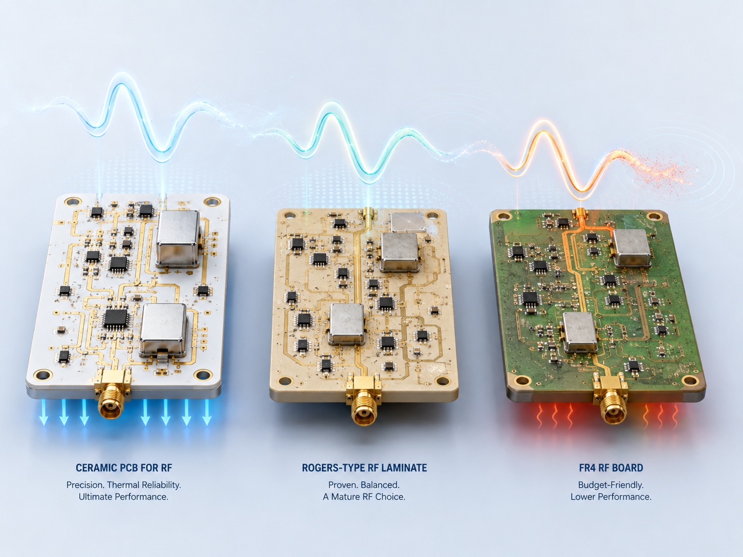
Aerospace PCB Applications We Can Support

Our aerospace-related PCB and PCBA solutions can be used in many electronic systems, depending on customer design and project requirements.

Typical applications include:

  • Avionics control modules
  • Satellite communication equipment
  • Radar and RF modules
  • UAV control systems
  • Navigation electronics
  • Power control units
  • Aerospace lighting systems
  • Sensor modules
  • Ground testing equipment
  • High-reliability industrial electronics
  • Defense-related electronic assemblies
  • Communication and telemetry systems

Each application has different requirements. Some need high-frequency performance. Some need compact structures. Some need better heat dissipation. Some need high-current capability. Some need rigid-flex design to reduce cables and connectors.

Frequently Asked Questions About Aerospace PCB Manufacturing

  • What is an aerospace PCB?

An aerospace PCB is a printed circuit board used in aerospace-related electronic systems, such as avionics, satellite communication, radar, UAV control, navigation, power control, and testing equipment. It usually requires higher reliability, better material control, stricter inspection, and stronger documentation than standard commercial PCB.

  • What types of PCBs are used in aerospace electronics?

Aerospace electronics may use rigid PCB, multilayer PCB, HDI PCB, rigid-flex PCB, RF PCB, heavy copper PCB, metal core PCB, ceramic PCB, and PCBA assemblies. The right type depends on space, signal, current, thermal, and reliability requirements.

  • What materials are suitable for aerospace PCB manufacturing?

Common material options include high-Tg FR4, polyimide, PTFE or RF laminates, heavy copper, aluminum base, copper base, and ceramic substrates. The best choice depends on working temperature, frequency, mechanical stress, heat load, and project requirements.

  • Do aerospace PCBs need IPC Class 3?

Many aerospace-related PCB projects may refer to IPC Class 3 or customer-specific high-reliability standards. However, the final requirement should always follow the customer drawing, procurement specification, acceptance standard, and application level.

  • Can you manufacture rigid-flex aerospace PCBs?

Yes. We can support rigid-flex PCB projects for compact and vibration-sensitive applications. Our engineering team can review bend areas, stack-up, coverlay design, stiffeners, copper structure, and assembly requirements before production.

  • Can ceramic PCBs be used in aerospace applications?

Yes. Ceramic PCBs can be used in aerospace-related applications that require high thermal conductivity, good electrical insulation, and dimensional stability. They are suitable for high-power modules, sensors, laser systems, and demanding thermal designs.

  • Do you provide aerospace PCB assembly?

Yes. We provide PCBA services, including SMT assembly, DIP assembly, component sourcing support, BGA assembly, X-ray inspection, functional testing, conformal coating, and box-build support when required.

  • What files are needed for an aerospace PCB quotation?

For PCB quotation, please send Gerber files, drill files, stack-up requirements, material requirements, copper thickness, surface finish, impedance requirements, quantity, lead time, and testing requirements. For PCBA, please also send BOM, CPL, assembly drawings, and testing instructions if available.

Need Aerospace PCB Manufacturing Support?

If you are developing aerospace-related electronics and need reliable PCB manufacturing or assembly support, EBest Circuit can help review your project before production.

We support high-Tg PCB, HDI PCB, rigid-flex PCB, RF PCB, heavy copper PCB, metal core PCB, ceramic PCB, multilayer PCB, and PCBA projects for demanding electronic applications.

Our engineering team can review your Gerber files, stack-up, material requirements, impedance control needs, testing requirements, assembly risks, and production feasibility. Whether you need prototype verification, small-batch production, or one-stop PCB assembly, we can help you choose a practical and reliable manufacturing solution.

Send your project files and requirements to sales@bestpcbs.com. Our team will help evaluate your aerospace PCB project and provide engineering support for quotation and production.

You may also like

RF & Telecom PCB Manufacturer

June 15th, 2026

RF & Telecom electronics depend on stable signal transmission. At high frequencies, small changes in material, dielectric thickness, copper roughness, impedance, stack-up, or surface finish can affect circuit performance. Because of this, RF & Telecom PCB manufacturing requires more than standard PCB fabrication. It needs suitable materials, controlled impedance, precise stack-up management, reliable testing, and engineering review before production.

RF & Telecom PCB Manufacturer

EBest Circuit supports RF and telecom PCB projects that require high-frequency materials, controlled impedance, multilayer stack-up control, thermal management, PCB assembly, and project documentation. Our capabilities include RF PCB, high-frequency PCB, HDI PCB, rigid-flex PCB, heavy copper PCB, metal core PCB, ceramic PCB, multilayer PCB, and PCBA services.

From RF PCB prototypes to telecom batch production, our engineering and manufacturing teams help customers review design feasibility, reduce manufacturing risks, and build reliable circuit boards for communication electronics.

Why RF & Telecom PCB Projects Need More Than Standard PCB Manufacturing?

RF & Telecom PCB refers to printed circuit boards used in radio frequency and communication electronics. These boards are commonly found in wireless communication products, antenna systems, RF front-end modules, radar electronics, satellite communication equipment, network devices, optical communication systems, and telecom infrastructure.

Unlike standard PCBs, RF and telecom PCBs must support stable signal transmission. At higher frequencies, a PCB trace is not just a copper connection. It acts as a transmission line. Its width, spacing, copper thickness, dielectric thickness, material properties, reference plane, and surface finish can all influence signal behavior.

This is why RF & Telecom PCB projects need a manufacturer with high-frequency PCB experience, not only a supplier that can build basic boards.

Customers usually need more than open and short testing. They may need controlled impedance, low signal loss, stable stack-up, consistent materials, impedance test reports, PCBA support, and clear production documentation.

At EBest Circuit, RF and telecom PCB manufacturing is handled as an engineering-driven process. We review material selection, stack-up, impedance targets, copper thickness, via structures, thermal paths, and assembly requirements before production when needed.

What Makes RF & Telecom PCBs Difficult to Build?

RF and telecom PCBs are difficult to build because small production variables can affect performance. A board may pass basic electrical testing but still perform poorly in an RF circuit if impedance, material loss, or signal transition is not controlled.

  • High-frequency signals are sensitive to dielectric constant and dissipation factor. If the material is not suitable for the operating frequency, signal loss may increase.
  • Controlled impedance is also critical. RF circuits often use 50-ohm single-ended impedance, while high-speed telecom circuits may require 90-ohm or 100-ohm differential impedance. Impedance can shift if trace width, spacing, dielectric thickness, or copper thickness is not controlled.
  • Stack-up design affects return paths, shielding, crosstalk, and signal stability. RF layers need proper reference planes and stable dielectric spacing. Poor stack-up planning may cause signal reflection, EMI issues, or inconsistent performance.
  • Via design is another key factor. Via transitions, via stubs, ground vias, and layer changes can affect RF and high-speed signals. The design must balance electrical performance and manufacturability.
  • Surface finish and copper profile may also influence high-frequency behavior. At higher frequencies, signal current tends to flow near the conductor surface, so copper roughness and surface treatment can affect loss.

Telecom equipment often needs stable performance over long operating periods. For base stations, antenna modules, RF front-end circuits, network devices, and optical communication equipment, repeatable manufacturing is as important as the first successful prototype.

Our RF & Telecom PCB Manufacturing Capabilities

EBest Circuit supports RF and telecom PCB projects across different board structures, materials, and production stages. We help customers choose suitable manufacturing solutions according to frequency, impedance target, thermal load, board size, assembly method, and production volume.

Our RF and telecom PCB capabilities include:

  • RF PCB for antenna modules, RF front-end circuits, wireless communication products, and microwave systems
  • High-frequency PCB using RF laminates and customer-specified high-frequency materials
  • Controlled impedance PCB for RF and high-speed telecom signals
  • Multilayer telecom PCB for communication equipment, network systems, and control modules
  • HDI PCB for compact communication products and high-density routing
  • Rigid-flex PCB for space-limited RF and telecom assemblies
  • Hybrid stack-up PCB combining RF materials with FR4 or other substrates
  • Heavy copper PCB for telecom power control and current-carrying circuits
  • Metal core PCB for RF power modules and thermal management applications
  • Ceramic PCB for high-power, high-heat, and dimensionally stable electronic modules
  • PCBA service for PCB fabrication, component sourcing, SMT assembly, inspection, testing, and box-build support

Different communication products require different PCB structures. An antenna module may require low-loss RF laminate and controlled impedance. A telecom control board may need multilayer FR4 with impedance control. A compact communication device may require HDI or rigid-flex PCB. A power amplifier module may need heavy copper, metal core, or ceramic PCB for heat dissipation.

Our engineering team can review the design and suggest a practical manufacturing route before production.

What Types of PCBs Are Used in RF and Telecom Equipment?

RF and telecom equipment can use different PCB types depending on frequency, signal speed, power level, mechanical layout, heat dissipation, and cost target.

RF PCB is used for radio frequency circuits, including antenna modules, RF front-end boards, wireless communication products, microwave systems, and signal transmission modules. RF PCB manufacturing requires careful control of material properties, impedance, dielectric spacing, copper thickness, and surface quality.

High-frequency PCB is used when the circuit works at higher frequencies and needs lower signal loss. These boards often use RF laminates, PTFE-based materials, ceramic-filled materials, or other high-frequency substrates. They are common in radar, microwave communication, satellite communication, and advanced wireless systems.

Telecom equipment often uses multilayer PCBs because the design may include RF signals, high-speed digital signals, power distribution, grounding, shielding, and control circuits. A stable multilayer stack-up helps improve routing density, signal integrity, and EMC performance.

Controlled impedance PCB is widely used in RF and telecom electronics. The board must be manufactured according to defined impedance targets. This requires coordination between design, material selection, stack-up, trace geometry, copper thickness, and manufacturing tolerance.

HDI PCB is suitable for compact telecom products, RF modules, IoT communication devices, and high-density control systems. Microvias, blind vias, buried vias, and fine lines help reduce board size while supporting complex routing.

Rigid-flex PCB can reduce connectors, save space, and improve mechanical reliability. It is suitable for compact communication equipment, antenna systems, portable RF modules, and assemblies where cable reduction is important.

Heavy copper PCB is used for power supply sections, current-carrying circuits, and telecom power modules. It improves current capacity and supports better heat spreading in power areas.

Metal core PCB helps transfer heat away from power components. Aluminum base and copper base PCBs can be used in RF power modules, LED communication modules, and telecom thermal management designs.

Ceramic PCB offers high thermal conductivity, dimensional stability, and electrical insulation. It can be used in high-power RF modules, microwave circuits, laser communication modules, and high-heat telecom applications.

Materials We Support for RF & Telecom PCB Applications

Material selection is one of the most important decisions in RF and telecom PCB manufacturing. The material affects impedance, signal speed, insertion loss, thermal behavior, dimensional stability, and cost.

EBest Circuit can support RF and telecom PCB projects using different material options based on customer requirements.

RF & Telecom PCB

High-frequency laminates are used when low loss and stable electrical performance are required. They are suitable for RF circuits, microwave circuits, antenna boards, satellite communication modules, and radar-related applications.

Rogers materials are commonly used in RF and microwave PCB applications because they offer more stable electrical properties and lower loss than standard FR4 in many high-frequency designs. They are often selected for antenna systems, RF modules, radar boards, and telecom equipment.

PTFE-based materials are widely used in RF and microwave circuits. They support low-loss signal transmission and stable dielectric behavior, making them suitable for high-frequency applications.

Not every telecom PCB requires RF laminate across the whole board. Some communication products use high-speed FR4 or high-Tg FR4 for digital, control, or power sections, while RF areas use special high-frequency materials.

Hybrid stack-up is useful when a design combines RF circuits with standard digital or power circuits. It can help balance performance and cost. However, hybrid material construction needs careful lamination control because different materials may have different thermal expansion and bonding behavior.

Aluminum and copper base materials can be used when RF or telecom modules generate heat. Metal core PCB helps improve heat transfer from power devices and supports stable operation in thermal-sensitive designs.

Ceramic substrates are suitable for compact, high-power, and high-heat RF or telecom modules. They provide good thermal conductivity, electrical insulation, and dimensional stability.

Material selection should be based on operating frequency, impedance target, insertion loss requirement, board thickness, thermal load, cost target, and production volume.

Controlled Impedance and Stack-Up Engineering Support

Controlled impedance is central to RF & Telecom PCB manufacturing. Many RF circuits use 50-ohm impedance. High-speed telecom circuits may require 90-ohm or 100-ohm differential impedance. Other values may also be used depending on the design.

Impedance is affected by:

  • Trace width
  • Trace spacing
  • Copper thickness
  • Dielectric thickness
  • Dielectric constant
  • Solder mask thickness
  • Reference plane distance
  • Stack-up structure
  • Manufacturing tolerance

If these factors are not controlled, the board may have impedance deviation. This can cause signal reflection, signal loss, timing issues, EMI problems, or unstable RF performance.

RF & Telecom PCB Manufacturer

Our engineering team can review your stack-up before production. This review may include dielectric thickness, copper thickness, layer arrangement, impedance targets, trace width, spacing, reference planes, solder mask influence, and impedance coupon design.

We can support different transmission line structures, including:

  • Microstrip
  • Stripline
  • Coplanar waveguide
  • Differential pairs
  • RF transmission lines
  • Controlled impedance signal layers

For projects that require impedance testing, we can review the test requirements and arrange impedance coupons according to the design. This helps customers confirm whether the manufactured board meets the required impedance range.

Signal Integrity, Loss Control, and RF Design Factors

RF and telecom PCB performance depends on the full signal path, including traces, vias, pads, connectors, reference planes, grounding, shielding, and layer transitions.

Insertion loss refers to signal loss through the transmission path. It can be affected by material dissipation factor, copper roughness, trace length, frequency, surface finish, and via transitions. Lower loss is important for many RF and telecom applications.

Return loss is related to signal reflection. If impedance is not well controlled, part of the signal may reflect back instead of continuing through the line. This can affect RF performance and communication quality.

Dense telecom boards may include many high-speed signals. Poor spacing, weak reference planes, or improper routing can increase crosstalk. Proper layer planning and routing rules help reduce interference.

Vias can create discontinuities in RF and high-speed paths. Via stub length, anti-pad design, ground via placement, and layer transition structure may affect signal performance.

RF circuits need stable grounding and proper shielding. Ground vias, via fences, reference planes, and shield cans may be used to reduce unwanted coupling and radiation.

Surface finish affects solderability, flatness, contact performance, and high-frequency behavior. The suitable finish should be selected according to RF performance, assembly requirements, storage needs, and customer specifications.

Many telecom products contain both RF circuits and high-speed digital circuits. These areas may have different design rules. A proper stack-up and grounding strategy can help reduce interference between functional sections.

Our team helps review manufacturability risks and production variables that may affect performance, including material selection, stack-up, copper thickness, impedance control, via structure, surface finish, and assembly feasibility.

Thermal Management for RF and Telecom Power Modules

RF and telecom PCB projects are not only about signal performance. Many communication products also generate heat. RF power amplifiers, base station modules, telecom power boards, LED communication devices, and power conversion circuits may require better thermal management.

Heat can affect component life, signal stability, solder joint reliability, and long-term product performance. If thermal paths are not designed properly, heat may concentrate around power devices.

Thermal management may involve:

  • Heavy copper for higher current and heat spreading
  • Thermal vias for heat transfer between layers
  • Copper balancing for manufacturing stability
  • Metal core PCB for heat dissipation
  • Copper base PCB for stronger thermal transfer
  • Aluminum base PCB for cost-effective heat dissipation
  • Ceramic PCB for thermal conductivity and electrical insulation
  • Component placement for shorter thermal paths
  • Heat sink connection areas
  • Thermal pad and solder mask opening control

EBest Circuit supports heavy copper PCB, metal core PCB, copper base PCB, aluminum PCB, and ceramic PCB for RF and telecom modules that require better heat dissipation.

For power-related telecom projects, our engineering team can review copper thickness, thermal vias, base material, heat transfer path, solder mask design, and assembly requirements before production.

Quality Control for RF & Telecom PCB Manufacturing

For RF and telecom PCB projects, quality control is not only open and short testing. It also includes stable materials, accurate stack-up, controlled impedance, plating consistency, and repeatable production.

Our quality control process can include:

  • Incoming material inspection
  • Engineering file review
  • Stack-up confirmation
  • Inner layer AOI
  • Lamination process control
  • Drilling inspection
  • Plating thickness control
  • Solder mask inspection
  • Surface finish inspection
  • Electrical testing
  • Impedance testing when required
  • Microsection analysis when required
  • Final visual inspection
  • Packing inspection
  • Traceability documentation

For controlled impedance projects, test coupons can be used to verify impedance performance. For multilayer telecom PCBs, stable lamination and dielectric thickness control are important. For RF PCBs, material handling, surface quality, and process consistency need careful control.

For PCBA projects, additional inspection can include:

  • BOM review
  • Component sourcing control
  • Solder paste inspection
  • SMT placement inspection
  • Reflow process control
  • AOI inspection
  • X-ray inspection for BGA or hidden solder joints
  • RF connector assembly inspection
  • Functional testing when required
  • Conformal coating when required
  • Final assembly inspection

Quality for RF & Telecom PCB manufacturing depends on correct material selection, practical stack-up, stable fabrication, controlled assembly, and clear inspection requirements.

PCB Assembly Support for RF & Telecom Electronics

Many customers need more than bare PCB fabrication. RF and telecom projects may require PCB assembly, component sourcing, RF connector assembly, shield can assembly, functional testing, and box-build service.

EBest Circuit provides PCB and PCBA one-stop support to help customers reduce supplier coordination work. Customers can combine PCB fabrication, component sourcing, SMT assembly, inspection, testing, and final packaging with one team.

RF & Telecom PCB Manufacturer

Our PCBA capabilities include:

  • SMT assembly
  • DIP assembly
  • Fine-pitch component assembly
  • BGA assembly
  • QFN and QFP assembly
  • RF connector assembly
  • Shield can assembly
  • Component sourcing support
  • BOM review
  • PCB fabrication and assembly coordination
  • SPI inspection
  • AOI inspection
  • X-ray inspection
  • Functional testing
  • Conformal coating
  • Box-build assembly

Assembly quality can affect RF and telecom product performance. Connector alignment, solder joint quality, shielding structure, cleaning, reflow profile, and component placement all need attention.

For projects that require testing, our team can review the customer’s functional test method before production. If special RF testing is required, we can discuss the test conditions and support production coordination based on customer specifications.

From RF PCB Prototype to Telecom Batch Production

RF and telecom projects often start with prototypes. Engineers may need to verify frequency performance, impedance, material choice, antenna behavior, thermal design, connector structure, and assembly feasibility before moving to batch production.

EBest Circuit supports customers through different project stages:

  • RF PCB prototype
  • Engineering sample
  • Design verification build
  • Small-batch production
  • Pilot run
  • Telecom batch production
  • Repeat order manufacturing
  • PCB assembly and testing
  • Box-build support when required

For prototype projects, customers often need fast feedback and practical manufacturability suggestions. Our engineering team can review the design and point out issues related to material, stack-up, drill design, impedance, copper thickness, or assembly.

For batch production, customers need stable material supply, repeatable processes, controlled inspection, and clear documentation.

Because we support both prototype and production stages, customers can move from early design review to later production with better continuity.

What Files Should You Send for an RF & Telecom PCB Quote?

A complete quotation package helps our engineering team evaluate your RF & Telecom PCB project faster and more accurately. Because RF and telecom designs are sensitive to materials and stack-up, complete information helps improve quotation accuracy.

For bare PCB fabrication, please prepare:

  • Gerber files
  • Drill files
  • Stack-up requirement
  • Material brand or material type
  • Target frequency if available
  • Impedance requirement
  • Copper thickness
  • Board thickness
  • Surface finish
  • Solder mask requirement
  • Silkscreen requirement
  • Controlled impedance tolerance
  • Impedance test requirement
  • Special via structure requirement
  • Quantity
  • Expected lead time
  • Testing requirement
  • Special documentation requirement

For PCBA projects, please also provide:

  • BOM
  • CPL or pick-and-place file
  • Assembly drawing
  • RF connector requirement
  • Shielding requirement
  • Functional test instruction if available
  • Programming requirement if needed
  • Conformal coating requirement if needed
  • Box-build documents if required

If your files are not complete, you can send the available files first. Our engineering team can help check what information is missing before quotation.

Why Choose EBest Circuit for RF & Telecom PCB Projects?

Choosing an RF & Telecom PCB manufacturer is about more than price. A supplier should be able to support material review, impedance control, stack-up engineering, thermal management, reliable manufacturing, PCBA, and technical communication.

EBest Circuit supports RF and telecom PCB projects through manufacturing experience, wide PCB capability, engineering support, quality control, and one-stop PCB assembly service.

Founded in 2006, EBest Circuit has long-term experience in PCB manufacturing and PCB assembly. We serve customers in communication electronics, industrial control, automotive electronics, medical devices, power electronics, aerospace-related electronics, and other high-reliability fields.

This experience helps us understand the requirements of RF and telecom projects, including materials, impedance, signal behavior, thermal performance, assembly quality, and production consistency.

Our capabilities include RF PCB, high-frequency PCB, controlled impedance PCB, multilayer PCB, HDI PCB, rigid-flex PCB, heavy copper PCB, metal core PCB, ceramic PCB, and PCBA.

RF & Telecom PCB Manufacturer

This gives customers more flexibility when choosing the right board structure for communication equipment, RF modules, antenna systems, power boards, and high-speed telecom products.

We do not only quote from Gerber files. Our engineering team can review material selection, stack-up, impedance targets, copper thickness, via structure, RF routing risks, thermal paths, and assembly feasibility before production.

We can support RF and telecom PCB projects using customer-specified high-frequency materials and controlled impedance requirements. Our team can review dielectric thickness, trace width, spacing, copper thickness, reference planes, and impedance coupons according to project needs.

We provide PCB fabrication, component sourcing support, SMT assembly, DIP assembly, inspection, functional testing, conformal coating, and box-build support. This helps customers reduce supplier management work and improve project communication.

We support RF PCB prototypes, engineering samples, small batches, pilot runs, batch production, and repeat orders. Customers can work with one manufacturing partner from early development to later production.

Our quality management approach supports controlled manufacturing, inspection, testing, and documentation. For projects with special quality, traceability, or inspection requirements, our team can review the details before production.

RF and telecom projects often involve technical questions. Our team can communicate with customers about material options, stack-up feasibility, impedance control, testing needs, assembly risks, and delivery planning.

Frequently Asked Questions About RF & Telecom PCB Manufacturing

  • What is an RF & Telecom PCB?

An RF & Telecom PCB is a printed circuit board used in radio frequency and communication electronics. Common applications include antenna modules, RF front-end circuits, wireless devices, base station equipment, radar modules, satellite communication systems, optical communication devices, and network equipment.

  • What is the difference between RF PCB and standard PCB?

A standard PCB mainly provides electrical connections. An RF PCB must also control signal loss, impedance, dielectric behavior, copper quality, grounding, shielding, and signal path stability. It usually requires more careful material selection and stack-up control.

  • What materials are used for RF PCB manufacturing?

RF PCB materials may include Rogers materials, PTFE-based materials, high-frequency laminates, ceramic-filled substrates, high-speed FR4, high-Tg FR4, metal core materials, and ceramic substrates. The best material depends on frequency, loss target, impedance requirement, thermal needs, cost, and production volume.

  • Can you manufacture Rogers PCB?

Yes. We can support RF and high-frequency PCB projects using Rogers materials and other customer-specified RF laminates. Please send your material requirement, stack-up, Gerber files, and impedance targets for engineering review.

  • Can RF PCB combine Rogers and FR4 materials?

Yes. Some RF and telecom designs use hybrid stack-up structures that combine RF materials with FR4 or other materials. This can help balance performance and cost, but it requires careful lamination and stack-up review before production.

  • Why is controlled impedance important for telecom PCB?

Controlled impedance helps maintain signal stability and reduce signal reflection, timing issues, and transmission problems. In telecom PCB designs, impedance is affected by trace width, spacing, dielectric thickness, copper thickness, material properties, and reference plane design.

  • What surface finish is suitable for RF PCB?

The suitable surface finish depends on RF performance, assembly method, storage requirement, solderability, and customer specification. Common options may include ENIG, immersion silver, OSP, or other finishes depending on project needs.

  • Do you provide RF PCB assembly?

Yes. We provide RF and telecom PCBA services, including SMT assembly, DIP assembly, RF connector assembly, shield can assembly, component sourcing support, AOI inspection, X-ray inspection, functional testing, conformal coating, and box-build support when required.

  • Can you support RF PCB prototypes?

Yes. We support RF PCB prototypes, engineering samples, small batches, pilot runs, and batch production. Our engineering team can review files before production to help reduce manufacturability risks.
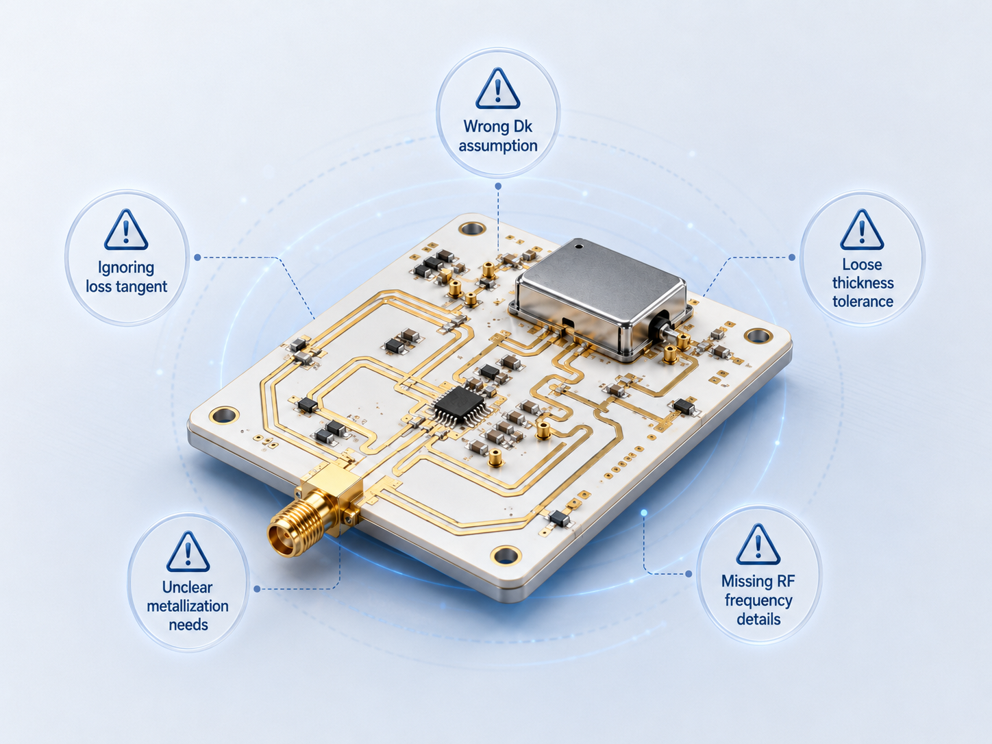
  • What files are needed for an RF & Telecom PCB quotation?

For PCB quotation, please send Gerber files, drill files, stack-up requirements, material requirements, impedance targets, copper thickness, board thickness, surface finish, quantity, and lead time. For PCBA quotation, please also send BOM, CPL, assembly drawings, and testing instructions if available.

Need RF & Telecom PCB Manufacturing Support?

If you are developing RF communication products, telecom equipment, antenna modules, radar electronics, wireless devices, optical communication systems, or high-speed signal boards, EBest Circuit can help review your project before production.

We support RF PCB, high-frequency PCB, controlled impedance PCB, multilayer telecom PCB, HDI PCB, rigid-flex PCB, heavy copper PCB, metal core PCB, ceramic PCB, and PCBA services for communication electronics.
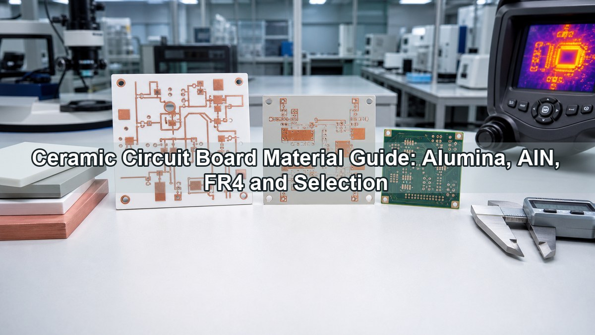
Our engineering team can review your Gerber files, stack-up, material requirements, impedance targets, copper thickness, thermal needs, assembly risks, and production feasibility. Whether you need RF PCB prototypes, small-batch builds, telecom batch production, or one-stop PCB assembly, we can help you choose a practical manufacturing solution.
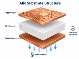
Send your project files and requirements to sales@bestpcbs.com. Our team will help evaluate your RF & Telecom PCB project and provide engineering support for quotation and production.

You may also like

5G Circuit Board Design, Prototype, Assembly, Turnkey Solutions

June 12th, 2026

Is a 5G circuit board project difficult due to RF loss, material mismatch, impedance issues, prototype failure, or assembly gaps? EBest provides design review, prototype support, PCB fabrication, assembly, and turnkey delivery to reduce production risk, improve manufacturability, and support stable high-frequency PCB performance.

What problems do OEM teams often face when sourcing 5G circuit board design, prototype, and assembly projects?

  • Design risk: Stack-up, RF layout, impedance rules, antenna area, via structure, and ground reference are not reviewed before production.
  • Material selection uncertainty: FR4, high-Tg FR4, Rogers, PTFE, hybrid stack-up, HDI PCB, or 5G flexible circuit boards are not matched to frequency, loss, heat, and cost targets.
  • Prototype failure risk: The first 5G circuit board prototype may fail because line width, spacing, dielectric thickness, copper roughness, and impedance control were not checked early.
  • Unclear prototype feedback: Test results, impedance data, soldering performance, and layout improvement points are not converted into clear changes before mass production.
  • Assembly handoff gaps: PCB fabrication and 5G circuit board assembly are handled separately, causing BOM mismatch, SMT placement issues, RF connector problems, or delayed testing.
  • Incomplete PCBA requirements: BOM, placement file, assembly drawing, polarity notes, shielding, functional test, and inspection standards are not fully confirmed before assembly.

EBest reduces these risks through early engineering review, prototype validation, and practical assembly support:

  • Design review: We review stack-up, impedance, RF trace rules, via structure, material, copper thickness, surface finish, and manufacturability.
  • Material matching: We match FR4, high-Tg FR4, Rogers, PTFE, hybrid stack-up, HDI PCB, or 5G flexible circuit boards based on frequency, heat, and structure.
  • Prototype support: We support small-batch builds to verify material, impedance, solderability, assembly fit, and production feasibility.
  • Prototype improvement: We review prototype feedback, impedance results, assembly issues, testing notes, and file updates before batch production.
  • PCBA coordination: We combine PCB fabrication and assembly to reduce BOM errors, SMT handoff delays, and RF component issues.
  • Assembly control: We provide BOM review, SMT, DIP, AOI, X-ray, RF connector assembly, shielding, functional testing, and custom inspection.

Welcome to contact us if you have any request for 5G circuit board manufacturing and assembly: sales@bestpcbs.com.

5G circuit board, https://www.bestpcbs.com/blog/2026/06/5g-circuit-board/

What Is a 5G Circuit Board?

A 5G circuit board supports RF signals, digital control, power paths, antenna modules, and high-speed data transmission. It requires tighter control of signal loss, impedance, heat, and interference than a standard PCB.

A 5G printed circuit board may use rigid PCB, HDI PCB, flexible PCB, rigid-flex PCB, high-frequency PCB, or hybrid stack-up.
The final structure depends on frequency band, antenna layout, signal path, assembly density, power level, and reliability target.

What Materials Are Used for 5G Circuit Boards?

Material choice affects RF loss, impedance stability, heat control, and PCB reliability. The right laminate should match frequency, stack-up, power level, and assembly method.

Material choice affects signal loss, impedance stability, thermal behavior, and PCB reliability.
High-Tg FR4 can support control circuits and lower-frequency areas.
Low-loss materials are better for RF paths, antenna sections, microwave circuits, and high-speed communication layers.

MaterialTypical UseKey ValueCommon Range
High-Tg FR4Control circuitCost controlTg 150–180°C
RogersRF pathLow lossDk 2.2–3.5
PTFEMicrowave areaStable dielectricDk 2.1–2.9
Hydrocarbon ceramicAntenna/RFLow DfDf 0.001–0.004
LCPFlexible RFLow moistureDk 2.9–3.2
Hybrid stack-upMixed circuitsBalanced cost4–20 layers

What Are the Main Types of 5G Circuit Boards?

Different 5G products require different PCB structures. The right type depends on RF performance, routing density, bending demand, product size, and assembly requirements.

Main 5G circuit board types include high-frequency PCB, HDI PCB, multilayer PCB, flexible PCB, and rigid-flex PCB.
Each type fits different product structures, RF requirements, assembly density, and space limits.

  • High-frequency PCB: Used for RF transmission, antenna paths, filters, and microwave circuits.
  • HDI PCB: Used for compact 5G modules with fine-pitch components and dense routing.
  • Multilayer PCB: Used for boards that combine RF, digital, power, and control circuits.
  • 5G flexible circuit boards: Used for antenna connections, compact wireless devices, and bendable structures.
  • Rigid-flex PCB: Used for folding structures, space-saving layouts, and stable interconnects.

Where Are 5G Circuit Boards Commonly Used?

5G circuit boards are used in products that require stable wireless signal, compact layout, and reliable assembly. Common areas include telecom, wireless modules, automotive connectivity, and industrial communication.

  • Base station modules: RF boards, antenna boards, power boards, and control boards.
  • Routers and gateways: High-speed wireless communication products.
  • Small cells: Compact indoor or urban 5G coverage devices.
  • Wireless modules: IoT, tracking, monitoring, and communication modules.
  • Automotive connectivity: V2X modules, telematics, and wireless control units.
  • Industrial communication devices: Remote monitoring, wireless control, and smart equipment.
5G Circuit Board Application, https://www.bestpcbs.com/blog/2026/06/5g-circuit-board/

What Are the Technical Requirements for 5G Circuit Boards?

A reliable 5G circuit board depends on controlled impedance, low-loss material, stable stack-up, thermal control, fine routing, and suitable surface finish.

Core requirements include impedance control, low-loss material, stable stack-up, thermal control, fine routing, and reliable finish.

ItemRecommended Control
Impedance tolerance±5% to ±10%
RF line widthBased on stack-up
Minimum line/space3/3 mil or tighter
Layer count4–20+ layers
Copper thickness0.5–3 oz
Surface finishENIG, ENEPIG, immersion silver
Via typeThrough, blind, buried, back-drilled
Thermal rangeProduct class
TestingE-test, AOI, impedance test

How to Design a 5G Circuit Board for High-Frequency Performance?

Good 5G circuit board design starts with frequency, stack-up, material, impedance, grounding, routing, vias, and heat control. These items should be reviewed before prototype production.

Design must control frequency, stack-up, material, impedance, RF routing, grounding, vias, and thermal management.

  • Confirm the working frequency first: This guides laminate choice, trace geometry, connector type, and antenna clearance.
  • Define the stack-up early: Control dielectric thickness, copper weight, layer order, and reference planes.
  • Choose the right PCB material: Use FR4 for control circuits and low-loss laminates for RF paths.
  • Control impedance: Match trace width, spacing, dielectric height, copper thickness, and solder mask rules.
  • Keep RF routing clean and short: Avoid unnecessary bends, stubs, vias, and sudden width changes.
  • Protect the reference ground plane: Continuous ground improves return current and reduces noise.
  • Manage via structure carefully: Use blind vias, buried vias, back-drilling, or via-in-pad only when required.
  • Separate RF, digital, and power sections: Use spacing, shielding, and grounding to reduce interference.
  • Plan heat dissipation early: Power amplifiers and RF modules require stable thermal paths.
  • Check DFM before fabrication: Confirm line width, spacing, holes, annular ring, solder mask, and panelization.

How Does the 5G Circuit Board Manufacturing Process Work?

The manufacturing process turns design files into a functional high-frequency PCB. For 5G PCB production, material control, copper quality, via reliability, and impedance consistency are critical.

Step-by-step process for 5G PCB production:

1. File review: Check Gerber, drill files, stack-up, impedance notes, BOM, placement files, and test requirements.

2. Material preparation: Prepare FR4, high-Tg FR4, Rogers, PTFE, LCP, or hybrid laminates; check batch, thickness, and copper foil.

3. Inner layer imaging and etching: Form inner circuits; control line width, spacing, copper balance, and registration.

4. Lamination: Press inner layers, prepreg, and copper foil to form multilayer stack-up; control pressure and temperature.

5. Drilling and via formation: Mechanical or laser drilling, blind/buried vias, back-drilling; ensure hole quality.

6. Copper plating: Plate through holes and via walls; check plating thickness and uniformity.

7. Outer layer imaging and etching: Form outer circuit; control trace width and spacing for RF paths.

8. Solder mask and surface finish: Apply solder mask and finish, such as ENIG, ENEPIG, or immersion silver.

9. Inspection and electrical testing: Use AOI, E-test, impedance coupon test, visual check, and dimension inspection.

10. PCB assembly if required: SMT, DIP, solder paste printing, component placement, reflow, AOI, X-ray, cleaning, and functional testing.

5G Circuit Board Manufacturing Process, https://www.bestpcbs.com/blog/2026/06/5g-circuit-board/

What Should Be Confirmed Before 5G Circuit Board Assembly?

Before assembly starts, BOM, placement file, polarity, RF components, soldering plan, inspection method, and testing requirements should be confirmed to reduce SMT errors and rework.

Confirm BOM, placement, polarity, RF components, solder paste, inspection, and test plan.

  • BOM: Part number, value, package, brand, tolerance, and alternatives.
  • Placement file: X/Y location, rotation, side, and reference designator.
  • RF components: Connectors, filters, amplifiers, shielding.
  • Polarity notes: Diodes, LEDs, ICs, tantalum capacitors.
  • PCB finish: ENIG, ENEPIG.
  • Soldering plan: Paste type, stencil thickness, reflow profile.
  • Inspection method: AOI, X-ray, visual, impedance, functional.
  • Special requirements: Shielding, programming, labeling, cleaning, conformal coating, packaging, fixture testing.

Why Choose EBest as Your 5G Circuit Board Manufacturer?

A strong 5G circuit board manufacturer should support material selection, design review, PCB fabrication, assembly, testing, and delivery in one clear workflow. EBest helps reduce communication gaps and production risk.

EBest helps reduce 5G circuit board project risk by combining material selection, design review, prototype validation, PCB fabrication, assembly, and inspection in one workflow.

With over 20 years of experience, EBest supports high-frequency PCB, HDI PCB, flexible PCB, rigid-flex PCB, RF PCB, and impedance control PCB projects. This provides clearer technical review, smoother production handoff, stable quality control, and faster quotation response.

  • Comprehensive PCB capabilities: FR4, multi-layer, metal-core, ceramic, semi-rigid flex, HDI, high-Tg, heavy copper, impedance control PCBs.
  • Expedited service: Urgent boards can be completed and shipped within 24 hours.
  • Strict quality certifications: IATF 16949, ISO 9001, ISO 13485, AS9100D, RoHS, REACH, UL.
  • Customized solutions: Personalized support, DFM review, material selection, and design verification.
  • Turnkey project support: End-to-end oversight from design review, prototype, fabrication, assembly, and functional testing.
5G Circuit Board, https://www.bestpcbs.com/blog/2026/06/5g-circuit-board/

Case Study: 5G Tower Circuit Board Project

This 5G tower circuit board project required stable RF performance, controlled impedance, thermal control, shielding, and reliable assembly. EBest managed the project from file review to prototype validation and batch production.

  • Project Background: A telecom provider needed a high-frequency 5G tower PCB integrating RF, antenna, power, and digital circuits.
  • Project Requirements: Stable RF, low insertion loss, controlled impedance, thermal management, SMT and through-hole assembly, shielding, functional testing.
  • Challenges: Complex multilayer stack-up, impedance ±5% tolerance, dense component placement, coordination of fabrication and assembly.
  • EBest Solutions: Full file review, low-loss laminate selection, prototype validation, integrated PCB fabrication and assembly, strict QC inspections.
  • Results: Prototype met RF, thermal, and assembly requirements; mass production achieved high yield and repeatable quality; on-time delivery with minimal revisions.

FAQs About 5G Circuit Boards

Q1: What file package is needed for a quote?
A1: Gerber, drill files, stack-up, impedance notes, BOM, placement file, assembly drawing, and test instructions.

Q2: Which materials are suitable for high-frequency 5G PCBs?
A2: Rogers, PTFE, LCP, hybrid stack-ups, and high-Tg FR4.

Q3: What inspections does EBest provide?
A3: AOI, X-ray, E-test, impedance testing, visual inspection, and functional testing.

Q4: Can EBest handle both prototype and volume production?
A4: Yes. Small-batch prototypes, pilot runs, and mass production are supported.

Q5: How is impedance controlled?
A5: Through stack-up design, trace width, spacing, dielectric thickness, copper thickness, and test coupons.

Q6: What is the typical layer count?
A6: 4–20+ layers, depending on RF routing, shielding, and component density.

Q7: What affects 5G circuit board cost most?
A7: Material type, layer count, impedance, copper thickness, via structure, surface finish, assembly scope, and testing requirements.

Get a Fast Quote for Your 5G Circuit Board Project

A clear quote starts with complete project files. Send Gerber, BOM, stack-up, impedance notes, and test requirements to EBest for fast review and practical production feedback.

EBest Circuit provides customized, high-frequency 5G PCB solutions from design review to turnkey delivery. Ensure your project meets RF, thermal, and assembly requirements efficiently. Contact us now at sales@bestpcbs.com to get a fast, accurate quote and professional support from concept to delivery.

You may also like

LED Lighting PCB Manufacturer

June 12th, 2026

LED Lighting PCB provides electrical connection, mechanical support, and heat dissipation for LED modules. EBest Circuit manufactures custom LED Lighting PCB using aluminum PCB, FR4 PCB, and turnkey assembly services for residential, commercial, high-power, automotive, and outdoor lighting projects.

Are you worried about these problems in LED Lighting PCB projects?

  • Delivery delays: Unstable production cycles, slow sample approval, material shortages, or batch delays may disrupt your project schedule.
  • Hidden costs: Extra charges may appear after quotation approval, including tooling changes, material upgrades, testing fees, or assembly adjustments.
  • Quality instability: Batch variation may cause flickering, overheating, soldering defects, color inconsistency, or field failure risks.
As a 20+ years PCB manufacturer, EBest Circuit provides manufacturing and assembly solutions for global lighting brands, OEM factories, and engineering projects.

  • Delivery predictability: ERP + MES production tracking supports 7-day standard delivery, 48-hour urgent response, and delay rate controlled at ≤2%.
  • Cost transparency: BOM-level cost modeling locks pricing before production and covers material, fabrication, assembly, testing, packaging, and export documentation.
  • Quality reliability: AOI inspection, flying probe testing, thermal validation, and functional testing support 100% critical process inspection, ≤0.3% defect rate, and ≥98% batch consistency.

Welcome to contact us if you have any request for LED lighting PCB manufacturing and assembly: sales@bestpcbs.com.

What Is an LED Lighting PCB?

An LED lighting PCB is a printed circuit board used to mount, connect, and power LED components in lighting products. It provides current paths, mechanical support, thermal transfer, and assembly stability for LED modules.

Unlike standard circuit boards, LED lighting boards must handle heat, current load, brightness stability, and long operating hours. Poor PCB quality may cause hot spots, unstable light output, solder joint fatigue, and early LED failure.

EBest Circuit manufactures custom LED PCB, aluminum PCB, FR4 PCB, and assembled LED modules for residential, commercial, industrial, automotive, and outdoor lighting applications.

Why Do LED Lighting Products Need Reliable PCB Solutions?

LED lighting products rely on stable PCB performance because heat, current, and soldering quality directly affect lifespan. A weak PCB may reduce brightness, increase failure rates, and raise after-sales cost.

Reliable PCB solutions help control:

  • Thermal stability: Better heat transfer reduces LED junction temperature.
  • Electrical safety: Stable copper design supports consistent current flow.
  • Assembly yield: Accurate pads and solder mask control reduce SMT defects.
  • Batch consistency: Controlled fabrication keeps repeated orders stable.
  • Long-term reliability: Better materials reduce delamination, oxidation, and early failure.

Choosing the right manufacturer affects warranty risk, brand reputation, and total project cost.

What LED Lighting PCB Types Can We Manufacture?

EBest Circuit manufactures LED lighting boards according to power level, heat dissipation demand, product structure, and assembly requirements. Instead of using one fixed PCB type, we help customers choose the right structure for actual working conditions.

Common PCB types include:

  • Aluminum LED PCB: Suitable for high-power LED modules, street lights, flood lights, panel lights, and outdoor lighting products.
  • FR4 LED PCB: Suitable for low-power and medium-power residential lighting, commercial lighting, control circuits, and cost-sensitive products.
  • Metal Core PCB: Designed for products that require stronger thermal performance, stable mechanical support, and long operating life.
  • Heavy Copper LED PCB: Used for products with higher current load, stronger power demand, or long continuous operation.
  • High TG LED PCB: Suitable for lighting products exposed to higher working temperature or repeated thermal stress.
  • Multilayer LED PCB: Used when modules include driver circuits, control functions, sensors, communication modules, or compact routing.
  • Flexible and Rigid-Flex LED PCB: Suitable for curved lighting structures, automotive lighting, wearable lighting, compact modules, and special installation spaces.

The right type should match LED power, thermal path, fixture housing, installation environment, and production cost.

Aluminum PCB vs FR4 PCB for LED Lighting

Aluminum PCB and FR4 PCB solve different lighting problems. The choice affects heat dissipation, electrical stability, product cost, assembly yield, and long-term reliability.

ItemAluminum PCBFR4 PCB
Thermal Conductivity1.0–3.0 W/m·K0.3–0.5 W/m·K
Copper Thickness1oz–3oz1oz–2oz
Best UseHigh-power LEDLow to medium-power LED
Heat ControlStrongLimited
CostHigherLower
ApplicationsStreet light, flood light, panel lightIndoor lamp, control PCB, low-power module

Aluminum PCB is better for high-power LED lighting because it transfers heat away from LED components more efficiently. This helps reduce hot spots, solder joint stress, brightness decay, and early failure.

FR4 PCB is better for low-power LED lighting where heat is easier to control. It is often used in indoor lamps, control boards, small LED modules, and commercial lighting products where cost control matters more than extreme thermal performance.

From a project cost view, aluminum PCB is usually more expensive because the material and processing requirements are higher. However, for street lights, flood lights, grow lights, and high-power modules, better heat dissipation can reduce field failure and after-sales cost.

FR4 PCB is practical when the LED current is lower, the fixture has a separate heat sink, or the board mainly supports control functions. It can reduce material cost, simplify production, and support multilayer routing more easily.

In short, choose aluminum PCB for high-heat lighting products and choose FR4 PCB for low-power or cost-sensitive lighting applications.

LED Lighting PCB Applications We Support

LED lighting boards are used in many lighting products, and each application has different priorities. Outdoor lighting focuses on heat, waterproof structure, and long service life. Indoor lighting focuses on cost, shape, brightness consistency, and assembly efficiency.

EBest Circuit supports PCB for:

  • Residential lighting: Ceiling lights, downlights, panel lights, and indoor lamps.
  • Commercial lighting: Office lighting, retail lighting, warehouse lighting, and display lighting.
  • Street lighting: High-power street light modules and aluminum PCB solutions.
  • Flood lighting: High-brightness PCB for outdoor and industrial lighting.
  • Grow lighting: Stable current and heat control for horticultural lighting.
  • Automotive lighting: Vehicle lamps, signal lights, and interior lighting.
  • Emergency lighting: Backup lighting systems and emergency light circuit boards.
  • Light bars and ring lights: Custom-shaped boards for compact lighting products.

For each application, we match material, copper thickness, LED layout, and assembly process to the final product structure.

LED Lighting PCB Applications

How Do We Improve Heat Dissipation for LED PCB?

Heat dissipation directly affects brightness stability, color consistency, solder joint life, and product lifespan. If heat is not controlled, LEDs may suffer brightness drop, color shift, solder fatigue, and early failure.

EBest Circuit improves thermal performance through:

  • Aluminum substrate selection: Aluminum PCB improves heat transfer for high-power LED modules.
  • Copper thickness optimization: 1oz, 2oz, or thicker copper supports current flow and heat spreading.
  • Thermal pad control: Proper LED pad design improves heat transfer from LED packages.
  • LED spacing optimization: Correct spacing reduces local hot spots and uneven heating.
  • Surface finish control: HASL and ENIG are selected based on soldering and reliability needs.
  • Thermal testing: Temperature rise is checked during sample validation and production testing.

For high-power projects, aluminum PCB, suitable copper thickness, and fixture-level thermal review are recommended before mass production.

What LED Lighting PCB Assembly Services Do We Provide?

EBest Circuit provides assembly services from bare PCB fabrication to finished LED modules. This helps customers reduce supplier coordination, shorten project cycles, and control quality from one source.

Assembly services include:

  • SMT assembly: For 2835, 5730, 3030, 5050, COB-related components, and LED driver parts.
  • Through-hole assembly: For connectors, terminals, switches, and power components.
  • Mixed assembly: For boards with both SMD and through-hole components.
  • Functional testing: Voltage, current, brightness, polarity, and continuity checks.
  • Turnkey service: PCB fabrication, component sourcing, assembly, testing, and packaging.

This service supports lighting brands, product developers, and OEM lighting manufacturers.

How Do We Control LED Lighting PCB Quality?

EBest Circuit controls quality from material inspection to final function testing. Each step reduces overheating, soldering defects, electrical failure, and batch inconsistency.

  • Incoming material inspection: We check substrate, copper thickness, solder mask, surface finish, and components before production.
  • PCB fabrication control: We inspect circuit accuracy, hole quality, solder mask alignment, board thickness, and surface finish.
  • AOI inspection: Automated optical inspection checks LED polarity, component placement, solder joints, missing parts, and visible SMT defects.
  • Electrical testing: Flying probe testing, E-test, or fixture testing checks open circuits, short circuits, and continuity.
  • Thermal validation: Aluminum PCB and high-power LED boards are checked for heat transfer and hot spot risk.
  • Functional testing: Assembled modules are powered under working voltage to verify brightness, current stability, polarity, and lighting behavior.
  • Final inspection: Board appearance, solder quality, markings, cleanliness, quantity, and packaging protection are checked before shipment.
  • Batch traceability: Production records, inspection results, and batch data are stored for follow-up and technical review.
LED Lighting PCB Quality Control

How Can We Help Optimize LED Light PCB Cost?

Cost optimization is not about choosing the cheapest board. It is about reducing unnecessary cost while keeping thermal performance, electrical stability, assembly yield, and long-term reliability under control.

Best Technology helps optimize cost through early engineering review, material selection, BOM checking, and production planning.

  • Choose the right material: Use aluminum PCB for high-heat products and FR4 PCB for low-power indoor lighting to avoid over-specification.
  • Optimize copper thickness: Select suitable copper weight based on current load and heat spreading. Too much copper increases cost, while too little copper increases heat risk.
  • Improve PCB size and panel utilization: Review board outline, spacing, and panel layout to reduce material waste and improve production efficiency.
  • Review LED layout before production: Proper spacing reduces hot spots, improves light uniformity, and avoids redesign after sampling.
  • Control BOM cost: Review LEDs, resistors, connectors, drivers, and other parts to find stable, cost-effective alternatives.
  • Reduce assembly defects: DFM review helps avoid solder bridging, wrong pad size, poor polarity marking, and SMT rework.
  • Verify prototype before mass production: Sample testing confirms thermal performance, brightness, current stability, and assembly quality.
  • Optimize order quantity: Proper batch planning reduces setup cost, material waste, packaging cost, and shipping cost per unit.

The final goal is stable LED performance, predictable delivery, and reliable mass production at a controlled total cost.

Case Study: High-Power LED Street Light PCB Project

Project Background
A European lighting customer was developing a high-power LED street light for city roads and industrial areas. Their previous supplier had unstable delivery, uneven batch quality, and poor heat dissipation, causing fixture assembly delays and higher project risk.

Project Requirements

  • Quantity: 5,000 high-power LED boards for outdoor street lighting.
  • Power: Support LED modules above 100W.
  • Material: Use aluminum PCB or high thermal conductivity material.
  • Quality: Control defect rate at ≤0.3% and batch consistency at ≥98%.
  • Compliance: Meet RoHS requirements.
  • Performance: Keep uniform light output, stable electrical performance, and long-term operation.

Project Solution

  • PCB structure optimization: Use 2oz aluminum PCB for better current capacity and heat spreading.
  • LED layout improvement: Adjust LED spacing and copper distribution to reduce hot spots and improve light uniformity.
  • Thermal management: Use high thermal conductivity aluminum substrate and optimized thermal paths.
  • Assembly control: Apply AOI inspection, electrical testing, thermal validation, and functional testing during production.
  • Delivery management: Use ERP + MES tracking to control schedule and reduce delivery uncertainty.

Project Results

  • On-time delivery: All 5,000 pieces were completed and shipped on schedule.
  • Stable thermal performance: Hot spot temperature was controlled below 45°C under defined test conditions.
  • Consistent quality: Batch consistency reached ≥98%, and defect rate was controlled at ≤0.3%.
  • Customer approval: The customer approved mass production and continued cooperation on related street light and flood light projects.

This project shows how Best Technology helps customers solve delivery, heat dissipation, and batch quality problems through proper material selection, production control, and full-process testing.

High-Power LED Street Light PCB

Why Choose EBest as Your LED Lighting PCB Manufacturer?

EBest Circuit, also known as Best Technology, is a China source PCB manufacturer with 20+ years of experience. We provide one-stop solutions from design support, prototype, and mass production to component sourcing, assembly, testing, and global delivery.

Here are reasons why choose EBest as your LED lighting PCB manufacturer:

  • Experienced manufacturer: 20+ years of PCB manufacturing experience reduces production risk.
  • One-stop service: Design support, prototype, mass production, sourcing, assembly, and testing are handled by one supplier.
  • Diverse PCB options: FR4, aluminum, metal core, heavy copper, high TG, multilayer, and impedance control PCB are available.
  • Strong production capacity: Monthly capability reaches 260,000 sq. ft / 28,900 sq. m, with 1,000+ boards completed monthly.
  • Fast delivery: Expedited boards can be shipped within 24 hours when project conditions allow.
  • Certified quality: IATF 16949, ISO 9001:2015, ISO 13485:2016, AS9100D, REACH, RoHS, and UL are supported.
  • Global supply: China source factory supply with worldwide shipping and export documentation.
  • Cost transparency: BOM-level cost planning helps lock total project cost before production.
  • Reliable quality: Critical processes are inspected, with defect rate controlled at ≤0.3% and batch consistency reaching ≥98%.
  • Custom project support: OEM and ODM services support residential, commercial, automotive, street light, flood light, grow light, and emergency lighting projects.

FAQs About LED Lighting PCB

Q1: What copper thickness is common for LED lighting PCB?
A1: Common copper thickness includes 1oz, 2oz, and 3oz. For high-power modules, 2oz copper is often used to improve current capacity and heat spreading.

Q2: What thermal conductivity is suitable for aluminum PCB?
A2: Common aluminum PCB thermal conductivity is 1.0–3.0 W/m·K. Higher thermal conductivity is better for high-power lighting with stronger heat output.

Q3: Can LED PCB be custom-shaped?
A3: Yes. Boards can be made in round, ring, bar, square, panel, or irregular shapes according to fixture structure and mounting requirements.

Q4: What surface finishes are common?
A4: HASL and ENIG are common. ENIG provides flatter pads and better solderability, especially for higher-reliability assembly projects.

Q5: Can you assemble 2835 and 5730 LEDs?
A5: Yes. We support 2835, 5730, 3030, 5050, and other standard SMD LED packages based on BOM and placement files.

Q6: What files are needed for quotation?
A6: Recommended files include Gerber, BOM, pick-and-place file, quantity, material, copper thickness, surface finish, and testing requirements.

Q7: How can I reduce LED PCB cost?
A7: Cost can be reduced by optimizing panel usage, material selection, copper thickness, BOM, DFM, and order quantity before production.

Q8: What causes LED PCB overheating?
A8: Common causes include poor thermal path, thin copper, dense LED spacing, weak substrate, or insufficient fixture-level cooling.

Q9: Do you provide prototypes?
A9: Yes. Prototypes help verify thermal performance, electrical stability, LED layout, brightness behavior, and assembly quality before mass production.

Q10: What is the typical lead time?
A10: Standard PCB orders can be completed in about 7 working days. Assembly lead time depends on BOM availability, quantity, and testing requirements.

Q11: Do you support outdoor LED projects?
A11: Yes. We support street lights, flood lights, grow lights, emergency lights, and other outdoor lighting products.

Q12: Can one order include aluminum and FR4 PCB?
A12: Yes. One project can include aluminum PCB for LED power modules and FR4 PCB for control circuits.

Q13: What defect rate is achievable?
A13: Under defined quality criteria, defect rate can be controlled at ≤0.3%, with batch consistency reaching ≥98%.

Q14: Do you provide global delivery?
A14: Yes. We support worldwide delivery by air, sea, or express, based on project urgency and order volume.

Q15: Can you review LED PCB design before production?
A15: Yes. We can review Gerber files, copper width, thermal path, panelization, pad design, and assembly risks before production.

Request a Quote for Your LED Lighting PCB Project

LED lighting PCB performance depends on material selection, heat dissipation, copper design, solder quality, and batch control. Aluminum PCB is suitable for high-power lighting, while FR4 PCB is practical for cost-sensitive indoor lighting.

For procurement, buyers should evaluate delivery stability, quality traceability, testing capability, material selection, and total project cost, not only unit price. EBest Circuit offers custom manufacturing, assembly, cost review, quality inspection, and global delivery from China.

Send your Gerber files, BOM, quantity, material requirement, and assembly details to sales@bestpcbs.com for a fast LED lighting PCB quotation.

You may also like

Reliable Industrial Control PCB Manufacturer with Early DFM Review

June 11th, 2026

Industrial Control PCB is a printed circuit board designed for automation equipment, industrial controllers, PLC modules, control panels, temperature control systems, and other factory control devices. This article explains how EBest Circuit (Best Technology) supports Industrial Control PCB projects with early DFM review, PCB fabrication, material matching, industrial PCBA support, and manufacturing risk control.

What problems do OEM buyers often face when sourcing Industrial Control PCB projects?

  • Incomplete files: Gerber, stack-up, drill, BOM, or test notes are missing.
  • Wrong PCB type: FR4, multilayer, HDI, flexible PCB, or metal base options are not confirmed.
  • Hidden production risk: Hole size, copper thickness, impedance, or solder mask rules are ignored.
  • PCBA handoff issues: PCB fabrication and industrial control PCB assembly are handled separately.
  • Unclear quotation: Industrial control PCB quotes vary because suppliers review different details.

EBEST reduces these risks through early engineering review and practical manufacturing support.

  • File check: We review Gerber, drill, stack-up, material, copper, and test notes before production.
  • PCB matching: We help match FR4, high-Tg FR4, multi-layer PCB, HDI printed circuit board, flexible PCB, or metal core PCB.
  • Process review: We check copper weight, line width, spacing, holes, impedance, solder mask, and finish.
  • PCBA support: We can add BOM review, SMT, DIP, AOI, X-ray when required, and customer-defined testing.
  • Clearer quote: We quote based on real manufacturability, not just board size and quantity.

​EBest Circuit (Best Technology) is a China industrial control PCB and PCBA manufacturer supporting industrial control FR4 PCB fabrication, industrial control PCBA, early DFM review, and turnkey project delivery. Our standard PCB capabilities include 1–50 layers, FR4 Tg 130–180 materials, 0.4–6.0 mm standard board thickness, FR4 inner copper from 0.5 oz to 6 oz, FR4 outer copper from 0.5 oz to 10 oz, controlled impedance, ENIG, ENEPIG, HASL, OSP, immersion tin, immersion silver, hard gold, soft gold, carbon ink, and gold finger plating. For industrial control PCB quotes, please send your Gerber files, stack-up, BOM, assembly drawing, copper thickness, surface finish, testing requirements, quantity, and delivery target to sales@bestpcbs.com.

Industrial Control PCB

What Should OEM Buyers Confirm Before Starting an Industrial Control PCB Project?

Industrial Control PCB projects should start with clear application and manufacturing requirements. This helps EBEST review whether the design can be built, assembled, tested, and repeated without unnecessary delays.

OEM buyers should confirm the following points before asking for industrial control PCB pricelist​:

  • Product use: PLC, control panel, motor control, sensor module, or temperature controller.
  • PCB type: FR4, multilayer, HDI, flexible PCB, metal base, or high-frequency PCB.
  • Board structure: Layer count, board thickness, copper weight, and stack-up.
  • Reliability needs: Tg, impedance, surface finish, solder mask, and testing method.
  • PCBA scope: Bare PCB only or PCB industrial controller assembly.

For example, a simple SMD PCB for industrial controller use may need standard FR4 and ENIG. A high-density PCB for industrial control systems may need finer line width, smaller vias, HDI structure, or controlled impedance. A control panel board with connectors and terminals may need stronger mechanical review and stable DIP assembly.

EBEST asks these questions early because industrial control boards often stay in production for years. A weak starting review can lead to repeat quotation changes, assembly problems, or unstable batch quality.

A clear project start gives the buyer a faster quote and gives the factory a better chance to control risk.

How Does EBEST Review Industrial Control PCB Files Before Production?

EBEST reviews Industrial Control PCB files before production to catch risks that may not be obvious from the board outline. The goal is not to slow the project down, but to prevent avoidable problems before fabrication and assembly.

Our early DFM review usually covers:

  • Gerber and drill file completeness
  • Layer count and stack-up
  • FR4 Tg requirement
  • Board thickness and tolerance
  • Inner and outer copper weight
  • Minimum line width and spacing
  • Minimum mechanical hole size
  • PTH and NPTH hole tolerance
  • Impedance requirement
  • Solder mask bridge and opening
  • Surface finish
  • Panelization and V-CUT design
  • Gold finger or edge connector area
  • BOM and assembly files if PCBA is required

EBEST’s standard PCB capability supports 1–50 layers and standard board thickness from 0.4 mm to 6.0 mm. For special projects, thinner, thicker, or higher-layer structures can be reviewed separately. This matters for industrial control system PCB projects because thick boards, dense routing, connectors, and repeated plugging can affect manufacturability.

For controlled impedance designs, EBEST reviews the stack-up, copper thickness, trace width, spacing, and impedance notes together. Our standard impedance tolerance is ±5Ω for impedance below 50Ω and ±10% for impedance of 50Ω or above.

A useful DFM review should tell the buyer what can be produced, what needs adjustment, and what may affect cost or lead time.

Which PCB Type Fits Industrial Control Applications?

Industrial control applications do not all use the same PCB type because signal density, current load, heat, space, and assembly needs are different.

EBEST can review the PCB type based on the actual control system.

Common options include:

  • FR4 PCB: Suitable for standard control boards, I/O modules, sensor interfaces, and general industrial controller circuits.
  • High-Tg FR4 PCB: Used for boards that need better heat resistance during assembly or long-term operation.
  • Multilayer PCB: Suitable for PLC modules, automation controllers, and dense industrial control system PCB designs.
  • HDI PCB: Used for compact controllers that need smaller vias, higher routing density, or limited board space.
  • Flexible PCB / Rigid-Flex PCB: Suitable for moving parts, compact wiring, vibration-sensitive modules, or reduced connector use.
  • Aluminum PCB: Used for LED industrial modules, thermal control areas, or power sections that need better heat spreading.
  • High-Frequency PCB: Suitable for industrial communication modules or control boards using RF or low-loss materials.

EBEST supports FR4 Tg 130–180 materials and can also review Rogers, Taconic, Arlon, Nelco, and other specified materials when required.

The best PCB type is the one that fits the product’s current, heat, density, reliability, and assembly needs.

How Does EBEST Manufacture FR4 and Multilayer PCB for Industrial Controllers?

FR4 and multilayer PCB are common choices for industrial controllers because they support stable routing, controlled cost, and long-term manufacturability. EBEST manufactures these boards by reviewing material, copper, layer count, drilling, solder mask, and surface finish before production.

For industrial controller PCB projects, EBEST can support:

  • 1–50 layer standard PCB production
  • FR4 Tg 130–180 material options
  • Standard board thickness from 0.4 mm to 6.0 mm
  • FR4 inner copper from 0.5 oz to 6 oz
  • FR4 outer copper from 0.5 oz to 10 oz
  • Mechanical finished hole size from 0.15 mm to 6.5 mm
  • Laser via minimum 0.10 mm under standard capability
  • Standard through-hole aspect ratio up to 12:1
  • Solder mask colors including green, black, blue, red, white, yellow, and others
  • Surface finishes including HASL, lead-free HASL, ENIG, ENEPIG, OSP, immersion tin, immersion silver, hard gold, and soft gold

For multilayer PCB for industrial controller projects, the stack-up is important. The material, copper distribution, dielectric thickness, via structure, and impedance requirement all affect both electrical performance and production stability.

For thick copper designs, line width and spacing must be reviewed together with copper weight. A 1 oz board cannot use the same routing rule as a 6 oz, 10 oz, or heavier copper board.

EBEST manufactures FR4 and multilayer industrial control PCB projects with process review first, so the final board is not only built, but built with repeatable rules.

What PCBA Support Can EBEST Add to Industrial Control PCB Projects?

Many industrial control projects do not stop at bare PCB fabrication. After the board is made, customers may still need industrial control PCB assembly, SMD assembly, DIP assembly, connector soldering, inspection, and functional test support.

EBEST can add PCBA support when the project needs a more complete manufacturing workflow:

  • BOM review and component sourcing review
  • SMT assembly for SMD PCB industrial controller projects
  • DIP assembly for connectors, relays, terminals, and large components
  • BGA/QFN assembly when required
  • AOI inspection
  • X-ray inspection when required
  • First article inspection
  • Customer-defined functional testing
  • Conformal coating or box-build support when required by the project

This is useful for industrial automation control panel PCB projects because these boards often include connectors, terminals, relays, communication ports, power input areas, and mixed SMT plus through-hole components.

If PCB fabrication and PCBA assembly are handled by different suppliers, the buyer may need to solve handoff issues alone. Common problems include incorrect component direction, unclear test points, poor connector fit, soldering difficulty, missing assembly notes, or late BOM changes.

EBEST’s value is to review the PCB and PCBA requirements together. This helps customers reduce repeated communication and improve project control from board fabrication to assembled controller board.

What Manufacturing Risks Should Industrial Control PCB Buyers Watch For?

Industrial Control PCB buyers should watch for manufacturing risks before the order enters production. Small details can become large problems when the board is used inside automation equipment or industrial controllers.

Common risks include:

  • Wrong material grade
    A low Tg material may not fit higher assembly or operating temperature needs.
  • Copper rule mismatch
    High copper weight needs wider line width and spacing.
  • Hole and board thickness conflict
    Small holes on thick boards may exceed practical aspect ratio limits.
  • Unclear impedance control
    Without stack-up and impedance notes, the supplier may not quote or build correctly.
  • Weak connector area
    Industrial control boards often need stable terminals, sockets, or gold finger contact areas.
  • Missing PCBA test plan
    Electrical testing does not replace functional testing for assembled control boards.

EBEST helps reduce these risks through early DFM review, process capability review, material confirmation, impedance review, surface finish review, PCBA planning, inspection, and customer-defined testing.

For example, if a buyer only asks for an industrial control PCB pricelist, the quote may miss key risks. A reliable industrial control PCB supplier should ask about the product use, board structure, copper weight, assembly scope, and test requirement.
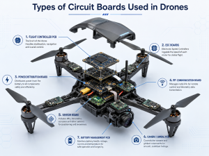
The best supplier is not the one that gives the fastest price. It is the one that finds problems before production.

Industrial Control PCB Case: How Did EBEST Support an Automation Control Panel Project?

An OEM customer needed an Industrial Control PCB for an automation control panel used in factory equipment. The board was used inside an industrial controller module, requiring stable signal control, connector reliability, and smooth PCBA assembly.

EBEST supported the project through the following steps:

  • Application review: The PCB was reviewed based on its use in an automation control panel and industrial controller module.
  • PCB specification check: EBEST checked the 6-layer FR4 structure, Tg150 material, 1 oz inner and outer copper, 1.6 mm board thickness, and ENIG surface finish.
  • Production file review: Gerber files, stack-up, copper thickness, board thickness, BOM, assembly drawing, connector areas, test points, and functional test requirements were reviewed before production.
  • PCB and PCBA support: EBEST supported PCB fabrication, BOM review, SMT assembly, DIP connector assembly, AOI inspection, FAI, and customer-defined functional testing.
  • Customer value: The customer reduced handoff risk between PCB fabrication, assembly, inspection, and testing.

Key project parameters:

  • Application: Automation control panel PCB
  • Product use: Industrial controller module
  • PCB type: 6-layer FR4 PCB
  • Material Tg: Tg150
  • Copper thickness: 1 oz inner and outer copper
  • Board thickness: 1.6 mm ±10%
  • Solder mask / silkscreen: Green solder mask, white silkscreen
  • Surface finish: ENIG
  • Gold thickness: Au 1 μin
  • Assembly support: SMT assembly and DIP connector assembly
  • Inspection and testing: AOI, FAI, and customer-defined functional testing
Industrial Control PCB

FAQs About Industrial Control PCB

What Is an Industrial Control PCB?
An Industrial Control PCB is a printed circuit board used in automation equipment, PLC modules, control panels, industrial controllers, motor control units, temperature controllers, and factory control systems.

Can EBEST Support Industrial Control PCB Assembly?
Yes. EBEST can support industrial control PCB assembly with BOM review, component sourcing review, SMT assembly, DIP assembly, AOI inspection, X-ray inspection when required, FAI, and customer-defined functional testing.

What PCB Types Are Used in Industrial Control Systems?
Common options include FR4 PCB, high-Tg FR4 PCB, multilayer PCB, HDI PCB, flexible PCB, rigid-flex PCB, aluminum PCB, and high-frequency PCB.

What Files Should I Send for Industrial Control PCB Quotes?
Please send Gerber files, drill files, stack-up, material notes, copper thickness, surface finish, BOM, pick-and-place file, assembly drawing, testing requirement, quantity, and delivery target.

Can EBEST Manufacture Bulk Industrial Control FR4 PCB Orders?
Yes. EBEST can support bulk industrial control FR4 PCB and repeat orders after confirming material, copper thickness, surface finish, tolerance, testing, and PCBA requirements.

Is EBEST an Industrial Control PCB Manufacturer in China?
Yes. EBest Circuit (Best Technology) is a PCB and PCBA manufacturer in China supporting OEM customers with Industrial Control PCB fabrication, assembly support, DFM review, and engineering communication.

In closing, industrial control PCB is designed for automation equipment, industrial controllers, PLC modules, control panels, temperature control systems, and factory control electronics. This article explained how OEM buyers can confirm project requirements, use EBEST’s early DFM review, select the right PCB type, manufacture FR4 and multilayer PCB, add PCBA support, avoid manufacturing risks, and learn from an automation control panel case.

EBest Circuit (Best Technology) supports Industrial Control PCB projects with PCB fabrication, early DFM review, FR4 and multilayer production, HDI PCB, heavy copper PCB, metal base PCB, high-frequency PCB, industrial control PCB assembly, inspection, and customer-defined testing. For your next Industrial Control PCB project, please send your files and requirements to sales@bestpcbs.com.

You may also like

Robotics PCB Manufacturer

June 11th, 2026

Is your robotics PCB still stable after motor startup, sensor feedback and real motion testing? Many robotics PCB problems do not appear during basic power-on checks. They usually appear when the motor starts, the sensor begins sending feedback, or the robot runs under vibration and heat. At that stage, voltage drop, signal noise, AI module heating and weak connector soldering can delay the whole project.

EBest is a China source factory for robotics PCB manufacturing, PCB assembly, component sourcing and testing. Founded in 2006, EBest supports motion control PCB, sensor PCB, robot power PCB and AI module PCB from prototype to mass production, helping robot projects move from early validation to stable batch production.

What Robotics PCB Problems Can EBest Help You Prevent?

EBest helps prevent unstable power, motor interference, sensor errors, AI module heating, solder joint failure and inconsistent batch quality before delivery. These issues often appear after basic power-on testing, especially when the robot starts moving under real motor load and vibration.

Common robotics PCB risks include:

  • Motor startup voltage drop that causes random reset
  • Sensor noise that affects detection and feedback
  • AI module heating that reduces long-term reliability
  • Weak connector soldering that fails under movement
  • Poor assembly consistency between prototype and batch production
  • Component sourcing delay before mass production
  • Insufficient testing before final delivery

A robotics PCB manufacturer should not only fabricate the board. It should review production risks, control soldering quality, check component availability and support testing before delivery.

How Does EBest Support Robotics PCB Manufacturing?

EBest supports robotics PCB manufacturing through PCB design, PCB prototype, mass production, component sourcing, PCB assembly, inspection and testing. This keeps production review, parts preparation, assembly and delivery in one controlled process.

  • PCB design and production review
    EBest can review Gerber files, BOM, pick-and-place files and assembly drawings before production. This helps check power areas, component spacing, connector positions, test points and assembly risks before the robotics PCB enters fabrication.
  • PCB prototype for early robot testing
    Prototype service helps verify motion control, sensor feedback, robot power PCB stability and AI module function before batch production. Early sample testing can expose voltage drop, signal noise, heat issues or connector risks before the project moves forward.
  • Component sourcing for BOM control
    EBest reviews component availability, package type, lead time and sourcing risk before assembly. This is important for robotics PCB projects that use motor drivers, sensors, wireless modules, AI processors, connectors and high-current power components.
  • PCB assembly for robot applications
    EBest supports SMT assembly, THT assembly and mixed assembly for robotics PCB projects. This fits boards that combine compact ICs, sensors, connectors, terminals, motor driver circuits and power components on one PCBA.
  • Mass production for repeat orders
    After prototype validation, EBest can support small batch, mid-volume robotics PCB assembly and high-volume robotics PCB assembly. Controlled assembly and inspection help keep board quality more consistent across repeat orders.
  • Inspection and testing before delivery
    EBest can support AOI inspection, X-ray inspection, electrical testing, power-on testing and functional testing based on project requirements. For robot PCB assembly service, testing should confirm power, signal, communication and key module functions before shipment.

This service flow helps robotics PCB projects move from design files to assembled boards with clearer production control, fewer supplier handoffs and better preparation before batch delivery.

Which Robotics PCB Applications Can EBest Build?

EBest can manufacture and assemble robotics PCBs for motion control, motor drivers, sensor systems, power boards, AI modules, wireless communication and automation equipment. This allows one supplier to support several board types within the same robot project.

Typical robotics PCB applications include:

  • Motion control PCB
  • Motor driver PCB
  • Robot power PCB
  • Sensor control PCB
  • AI robot module PCB
  • AI robotics PCB manufacturing
  • Wireless communication PCB
  • Line follower robot PCB
  • Line following robot PCB
  • Inspection robot PCB
  • Industrial robot control PCB
  • Service robot PCB
  • Educational robot PCB

These boards often combine power, signal, communication and mechanical stress. As a result, PCB quality, component placement and inspection control directly affect robot operation.

Robotics PCB Applications

How Does PCB Quality Affect Robot Motion Accuracy?

PCB quality affects robot motion accuracy through power stability, motor driver performance, encoder signal quality, EMI control and assembly consistency. If the motor driver cannot receive stable current, the robot may move with delay, drift or random stop.

Motion control PCB projects usually include drivers, controllers, encoders, connectors and power circuits. When motor EMI affects encoder or control signals, the robot may move incorrectly even when the software logic is right.

For this reason, robotics PCB design should review power trace width, grounding, EMI separation, connector strength and test points before production. During assembly, accurate placement and strong solder joints help keep batch robots performing consistently.

Key review points include:

  • Motor control voltage: commonly 5V-48V
  • Control signal level: commonly 1.8V-5V
  • Encoder signal type: digital or analog
  • PCB copper weight: commonly 1oz-3oz
  • Test point spacing: commonly 1.0mm-2.54mm

How Do Sensor PCBs Improve Signal Stability in Robots?

Sensor PCBs improve signal stability by supporting clean grounding, low-noise routing, accurate component placement and reliable connector assembly. Stable sensor input helps robots detect objects, follow paths, avoid obstacles and control movement feedback.

In a line follower robot PCB, unstable sensor signals may cause the robot to drift, stop or misread the path. In inspection robots, poor signal quality may affect detection accuracy and response time.

Therefore, sensor PCB production should focus on grounding, connector quality, component polarity and signal integrity. EBest supports PCB in robotics applications where sensor stability must be checked together with assembly quality and testing requirements.

What Makes AI Robotics PCB Assembly More Challenging?

AI robotics PCB assembly is more challenging because AI modules often require stable power, thermal control, high-density SMT placement, camera interfaces and multi-sensor connections. The main risks are high current load, heat concentration, signal interference and hidden soldering defects.

AI robot power PCB projects may place processors, memory, wireless modules, sensors and power circuits in a compact area. If the assembly process is not controlled, BGA, QFN or small-pitch components may create hidden soldering defects.

AI robot testing PCB requirements should go beyond simple power-on checks. The test should confirm power stability, communication, sensor interface, camera connection and module operation before delivery to improve AI robot PCB reliability.

Robotics PCB Assembly

What Should Be Reviewed Before Robotics PCB Production?

Power layout, grounding, EMI control, thermal design, connector placement, component spacing, test points and BOM availability should be reviewed before robotics PCB production. This helps reduce rework before PCB fabrication and assembly begin.

A practical robotics PCB production review should check whether high-current areas are wide enough, whether sensor signals are protected from motor noise, and whether connectors can handle movement and vibration.

BOM review is also important. If key components are obsolete, out of stock or difficult to source, the project may face delay before batch assembly. EBest reviews these risks early so customers can adjust before production.

Production review should cover:

  • Power trace width for current capacity and heat control
  • Grounding design for signal and power return paths
  • EMI control for motor and switching noise reduction
  • Thermal layout for drivers, regulators and AI modules
  • Connector position for vibration-sensitive areas
  • Component spacing for SMT assembly clearance
  • Test point access for production testing
  • BOM availability for sourcing and lead time control

How Does PCB Assembly Quality Reduce Robotics PCB Failure Risk?

PCB assembly quality reduces robotics PCB failure risk by improving solder joint strength, connector reliability, component placement accuracy and inspection consistency. This is important for robot boards that work under movement, vibration, heat and repeated load changes.

Cold solder joints, insufficient solder, wrong polarity and shifted components may pass simple power-on checks. However, they can cause random failure during long-term robot operation or during system-level testing.

For robotics PCB assembly, SMT precision matters for ICs, sensors and communication modules. THT quality matters for terminals, connectors and power parts. Mixed assembly is useful when one robot board combines compact SMT devices with high-current components.

Assembly risk points include:

  • Cold solder joints that cause intermittent failure
  • Insufficient solder on high-current pads
  • Wrong polarity components that damage power circuits
  • Connector solder cracks under vibration
  • Shifted components that affect signal or power paths
  • Flux residue that may affect long-term reliability
  • Batch inconsistency between prototype and repeat orders

What Tests Are Needed Before Robotics PCB Delivery?

AOI, X-ray inspection, electrical testing, functional testing, power-on testing, thermal review and customized reliability testing may be required before robotics PCB delivery. The final test plan should match the robot’s working environment and board function.

Common robotics PCB tests include:

  • AOI inspection for SMT placement and soldering quality
  • X-ray inspection for BGA, QFN and hidden solder joints
  • Electrical test for open and short circuit checking
  • Functional test for power, signal and communication
  • Power-on test for basic operating confirmation
  • Thermal review for motor drivers, regulators and AI modules
  • Connector inspection for vibration-sensitive applications
  • Custom robot PCB reliability test based on project requirements

These tests help reduce delivery risk before the robot enters full system testing. For AI robot testing PCB projects, power, signal and communication checks should be confirmed before shipment.

Case Study: Reducing Motion and Sensor Issues Before Batch Production

A robotics PCB project can pass basic power-on testing but still fail during real movement if motor load, sensor noise, vibration and soldering quality are not controlled before batch production. This case shows how production review helps reduce motion and sensor risks before mid-volume assembly.

Project Background

The customer was developing a mobile robot control board for motor control, sensor feedback and power distribution. The prototype could power on, but the board reset when the motor started. During movement testing, the sensor signal also became unstable, which affected motion accuracy and feedback reliability.

Customer Requirements

The project required stable power delivery, lower motor interference, stronger connector soldering, cleaner sensor feedback and consistent PCB assembly quality. The customer also wanted to reduce repeated prototype rework before moving to batch production.

Our Solution

EBest reviewed the Gerber files, BOM, assembly drawing and testing requirements before production. Our team checked high-current power areas, grounding paths, connector positions, component sourcing risks and assembly feasibility. During production, EBest controlled SMT placement, THT soldering, connector assembly, inspection and functional testing.

Output Result

The project moved from prototype validation to mid-volume robotics PCB assembly with lower production risk. The board showed lower reset risk during motor startup, more stable sensor feedback during movement and better consistency before robot system-level testing.

Key results included:

  • Lower motion failure risk during motor startup
  • More stable sensor feedback during robot movement
  • Stronger connector soldering for vibration-sensitive areas
  • Better batch consistency before mid-volume production
  • Less rework before final robot system testing
  • Faster transition from prototype validation to batch assembly

Why Choose EBest for Robotics PCB Manufacturing?

EBest provides PCB fabrication, component sourcing, PCB assembly, testing support and batch production service from one China source factory. For robotics PCB projects, this helps reduce supplier handoff, shorten communication time and lower production risk before delivery.

  • One-stop PCB and PCBA service
    EBest supports PCB design, PCB prototype, mass production, component sourcing and PCB assembly in one service flow. This keeps board production, parts sourcing and assembly communication in the same production chain.
  • 20+ years of PCB manufacturing experience
    Founded on June 28, 2006, EBest Circuit, also known as Best Technology, has over 20 years of PCB manufacturing experience. This supports robotics PCB production review from prototype verification to stable batch production.
  • Monthly production capability
    EBest’s monthly production capability reaches 260,000 square feet / 28,900 square meters, with more than 1,000 different boards completed monthly. This capacity supports prototype runs, repeat orders, mid-volume robotics PCB assembly and high-volume robotics PCB assembly.
  • Expedited service for urgent boards
    For urgent boards, EBest can provide expedited service, and eligible urgent boards can be shipped within 24 hours when project files, materials and production conditions allow. This is suitable for robotics PCB prototype verification and pilot production schedules.
  • Wide robotics PCB structure support
    EBest supports FR4 PCB, multi-layer PCB, Metal Core PCB, Ceramic PCB, flexible PCB, rigid-flex PCB, RF PCB, High Tg PCB, heavy copper PCB, HDI PCB, high-speed PCB, impedance control PCB and busbar PCB. These options fit robot power PCB, sensor PCB, motion control PCB and AI module PCB requirements.
  • SMT, THT and mixed assembly capability
    EBest supports SMT assembly, THT assembly and mixed assembly for robotics PCB projects. This is important for boards that combine compact ICs, sensors, connectors, terminals and high-current power components.
  • Certified quality and compliance systems
    EBest holds IATF 16949, ISO 9001:2015, ISO 13485:2016, AS9100D, REACH, RoHS and UL. These certifications support process control, material compliance and quality management for global B2B applications.
  • China source factory with global delivery
    EBest does not claim overseas factories, overseas warehouses or local branches. The service is based on China source-factory manufacturing, component sourcing, PCB assembly and global delivery support.

For robotics PCB assembly, EBest supports motion accuracy, sensor stability, AI robot PCB reliability and batch delivery through controlled manufacturing, assembly and testing.

Robotics PCB

What Files Should You Send for a Robotics PCB Quote?

Send Gerber files, BOM, pick-and-place file, assembly drawing, quantity, testing requirements and special notes about motor load, vibration, heat or working environment for a robotics PCB quote. Complete files help EBest review cost, lead time and production feasibility faster.

Recommended quote files include:

  • Gerber file in RS-274X format
  • BOM in XLS, XLSX or CSV format
  • Pick-and-place file in CSV or TXT format
  • Assembly drawing in PDF format
  • PCB stack-up if required
  • Surface finish requirement
  • Order quantity in units or panels
  • Testing requirement in PDF or TXT format
  • Special notes for motor load, vibration, heat or working environment

If the project includes AI modules, high-current motor drivers or critical sensors, share the test method and operating condition early. This allows a more accurate production review and reduces repeated confirmation before quotation.

FAQs About Robotics PCB Manufacturing

Q1: What is the MOQ for robotics PCB assembly?
A1: The MOQ depends on PCB complexity, component sourcing and testing requirements. For prototype projects, EBest can support small trial orders. For repeat production, mid-volume or high-volume robotics PCB assembly is more suitable after the design, BOM and test process are stable.

Q2: Can EBest source components for robotics PCB assembly?
A2: Yes. EBest can support component sourcing based on the customer’s BOM. Before assembly, the team can review part numbers, package types, availability and lead time risks. For motor drivers, sensors, connectors and AI modules, early BOM review helps reduce production delay.
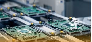
Q3: What affects the cost of a robotics PCB project?
A3: The main cost factors include PCB layer count, board size, copper weight, surface finish, component quantity, package difficulty, assembly type, testing scope and order volume. BGA, QFN, fine-pitch parts, high-current areas and functional testing can increase the total project cost.

Q4: Should I send a test fixture for robotics PCB functional testing?
A4: If the board requires motion control, sensor feedback, communication or AI module verification, a test fixture is recommended. A fixture helps confirm power, signal and interface functions more consistently before shipment, especially for batch robotics PCB assembly and repeat orders.

Q5: Can EBest handle alternative components if some parts are out of stock?
A5: EBest can help review possible alternative components, but final approval should come from the customer. For robotics PCB projects, replacement parts must match package size, electrical rating, tolerance, temperature range and functional requirements before they are used in production.
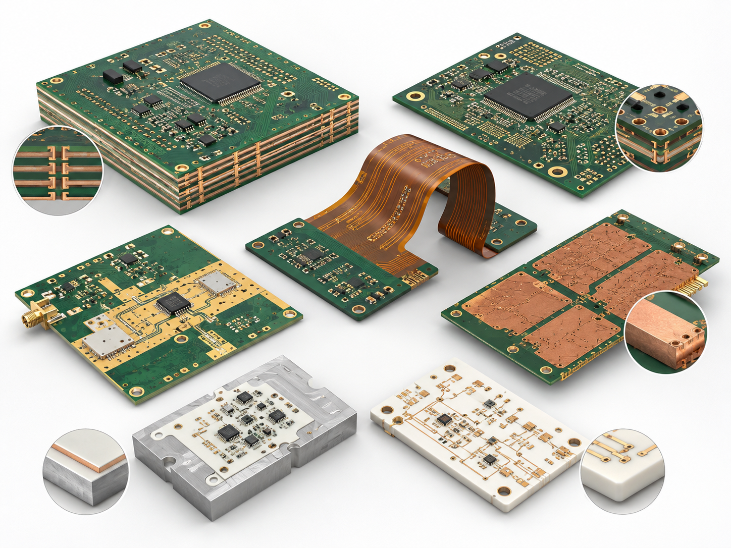
Q6: What files are required for faster robotics PCB quotation?
A6: For faster quotation, send Gerber files, BOM, pick-and-place file, assembly drawing, quantity and testing requirements. If the robotics PCB includes motor drivers, sensors, AI modules or high-current circuits, include operating conditions and special inspection notes early.

Q7: Can EBest support both prototype and batch robotics PCB production?
A7: Yes. EBest supports PCB prototype, small batch, mid-volume and high-volume robotics PCB assembly. Prototype production is used for function verification, while batch production focuses on assembly repeatability, inspection control, component supply and delivery consistency.

Q8: What should be confirmed before moving from prototype to batch production?
A8: Before batch production, confirm circuit function, BOM stability, test method, component availability, connector strength, thermal performance and assembly process. For robotics PCB projects, motor load, sensor stability and AI module power behavior should be checked before scaling.

Q9: Can EBest assemble robotics PCBs with both SMT and THT parts?
A9: Yes. EBest supports SMT, THT and mixed assembly. This is useful for robotics PCB projects that combine small ICs, sensors, wireless modules, connectors, terminals and high-current power components on the same board.

Q10: What surface finish is suitable for robotics PCB manufacturing?
A10: Common surface finishes include HASL, lead-free HASL, ENIG and OSP. The right choice depends on component package, soldering requirement, shelf life, cost and reliability needs. For fine-pitch components, BGA or AI module boards, ENIG is often considered during production review.

Q11: How can robotics PCB batch consistency be improved?
A11: Batch consistency can be improved through stable BOM control, clear assembly drawings, approved process settings, AOI inspection, soldering control, functional testing and consistent packaging. For robotics PCB assembly, repeatable production control is important because small defects may affect robot movement or sensor feedback.

Q12: Can EBest support urgent robotics PCB prototype orders?
A12: EBest can provide expedited service for urgent boards when project files, materials and production conditions allow. Eligible urgent boards can be shipped within 24 hours. For faster handling, customers should provide Gerber files, BOM, quantity and assembly requirements at the beginning.

Q13: What certifications does EBest have for PCB manufacturing?
A13: EBest holds IATF 16949, ISO 9001:2015, ISO 13485:2016, AS9100D, REACH, RoHS and UL. These systems support process control, quality management and compliance needs for global B2B PCB projects, including robotics PCB manufacturing and assembly.

Q14: Can a China source factory support overseas robotics PCB projects?
A14: Yes. A China source factory can support overseas robotics PCB projects through custom manufacturing, component sourcing, PCB assembly, testing and global delivery. EBest does not claim overseas factories, overseas warehouses or local branches. The service is based on China source-factory production.

Get a Robotics PCB Quote for Your Project

A reliable robotics PCB should support stable motion, clean sensor feedback, controlled power delivery and tested assembly quality before it enters real robot operation. For motion control boards, sensor boards, AI robot modules and robot power PCB projects, early production review can reduce rework, prevent batch inconsistency and lower delivery risk.

For selection, choose a robotics PCB manufacturer that can review design files, source components, assemble SMT and THT parts, inspect solder quality and support functional testing. For procurement, prepare complete Gerber files, BOM, pick-and-place files, quantity and test requirements before requesting a quote.

EBest Circuit is a China source factory supporting robotics PCB manufacturing and assembly, component sourcing, testing and global delivery for robot projects. Send your Gerber files, BOM, quantity and testing requirements to sales@bestpcbs.com for a robotics PCB manufacturing and assembly quote.

You may also like