





GND shielding is often discussed when a PCB project has noise, EMI, high-speed signals, RF areas, cable shields, USB connectors, CAN interfaces, sensors, or metal enclosures. For engineers, the question is not only “What is ground?” but “How should shielding connect to GND, and how can the approved layout be manufactured reliably?”
EBest Circuit (Best Technology) supports PCB fabrication, PCB layout manufacturability review, DFM checking, controlled impedance production, component sourcing, PCBA assembly, inspection, and testing coordination. If your project has GND shielding, shield GND, connector shielding, cable grounding, EMI, or PCBA shielding requirements, please feel free to send your Gerber files, stackup, BOM, drawings, impedance notes, and assembly requirements to sales@bestpcbs.com for engineering review before production.
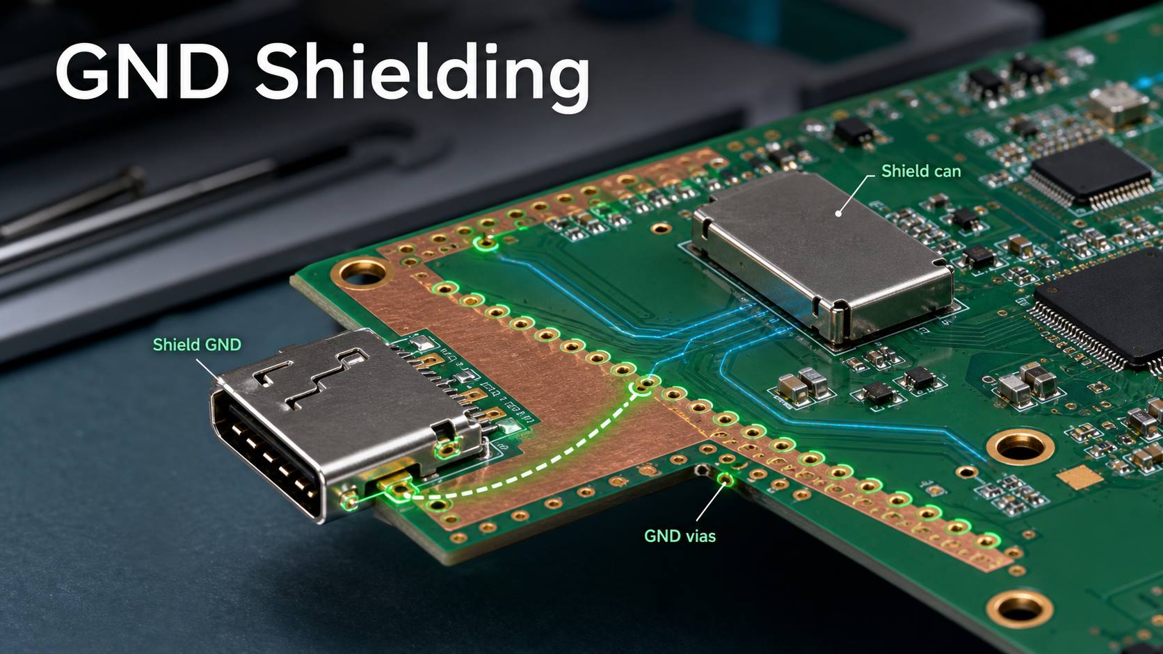
GND Shielding in PCB Layout Basics
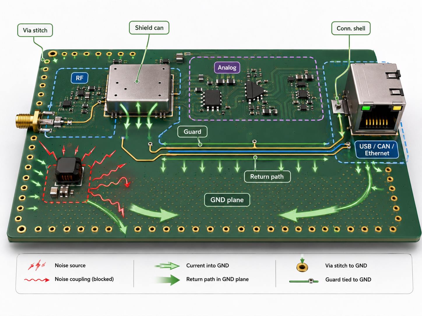
GND shielding means using ground-related structures to reduce unwanted noise coupling and improve signal stability. In PCB layout, it may include ground planes, guard traces, via stitching, shield connection pads, connector shell grounding, shielding cans, or controlled return paths.
The purpose is not to “block everything” with copper. A useful GND shielding structure should provide a low-impedance path for noise current and a stable reference for sensitive signals.
In real PCB projects, GND shielding is often used around:
- High-speed digital traces
- RF or antenna areas
- Analog sensor circuits
- USB, CAN, Ethernet, or other connector zones
- Cable shield termination points
- Shielding cans or metal enclosure contact areas
- Mixed-signal boards with noise-sensitive sections
In many projects, GND shielding is only one part of a broader PCB EMI shield strategy, especially when the board includes high-speed signals, RF areas, connectors, shield cans, or metal enclosure contact points.
For a PCB manufacturer, the responsibility is to protect the approved shielding intent during manufacturing. That means checking stackup, copper thickness, spacing, solder mask openings, via quality, impedance requirements, and assembly details before production.
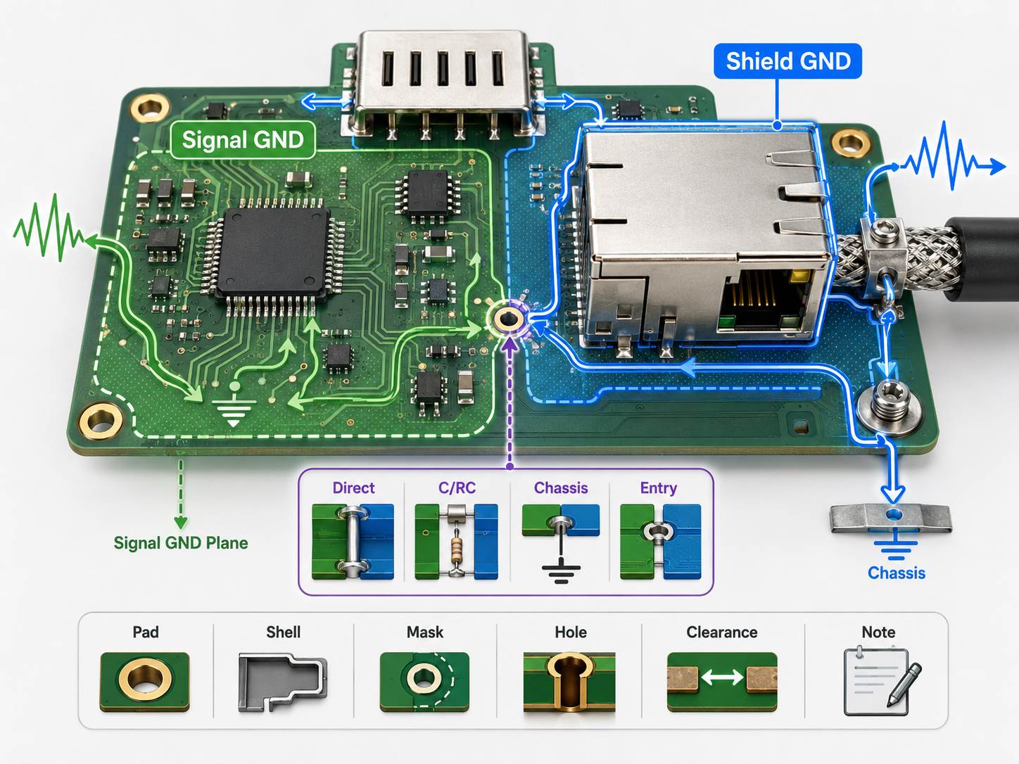
Shield GND vs Signal GND in PCB Projects
Shield GND and signal GND are related, but they are not always the same node in a product.
- Signal GND is usually the circuit reference used by components and signals.
- Shield GND is often related to cable shields, connector shells, chassis ground, enclosure contact, or EMI shielding structures.
Depending on the product, shield GND may be connected to signal GND directly, connected through a capacitor or RC network, connected to chassis ground, or handled at a specific entry point near the connector. The correct method depends on the customer’s circuit design, EMC strategy, safety requirements, and product environment.
From a manufacturing view, the key checks include:
- Is the shield pad clearly defined in the Gerber?
- Is the connector shell footprint manufacturable?
- Are solder mask openings correct?
- Is the copper area large enough for reliable soldering?
- Are vias, slots, or mounting holes placed correctly?
- Are clearance and creepage requirements respected?
- Does the assembly note match the PCB drawing?
EBest Circuit does not guess the customer’s grounding architecture. Our role is to review whether the approved layout can be manufactured and assembled as intended.
Ground Shield for High-Speed Signals and EMI Control
A ground shield can help high-speed and noise-sensitive signals when it is placed and connected correctly. The most common method is a solid reference plane under controlled traces, because the return current needs a continuous path.
If a high-speed signal crosses a split ground plane, the return path may be interrupted. This can increase loop area, noise, EMI risk, and signal integrity problems. For impedance-controlled boards, the trace width, dielectric thickness, copper thickness, and reference layer must be reviewed together.
Useful PCB shielding structures may include:
- Continuous GND reference planes
- Ground copper near sensitive areas
- Guard traces for high-impedance analog signals
- Via stitching along board edges
- Via fences near RF or noisy zones
- Shield can grounding pads
- Connector shell grounding pads
The layout decision belongs to the customer’s engineering team. The manufacturing review should confirm that these structures can be produced consistently without causing solder mask, spacing, plating, or assembly issues.
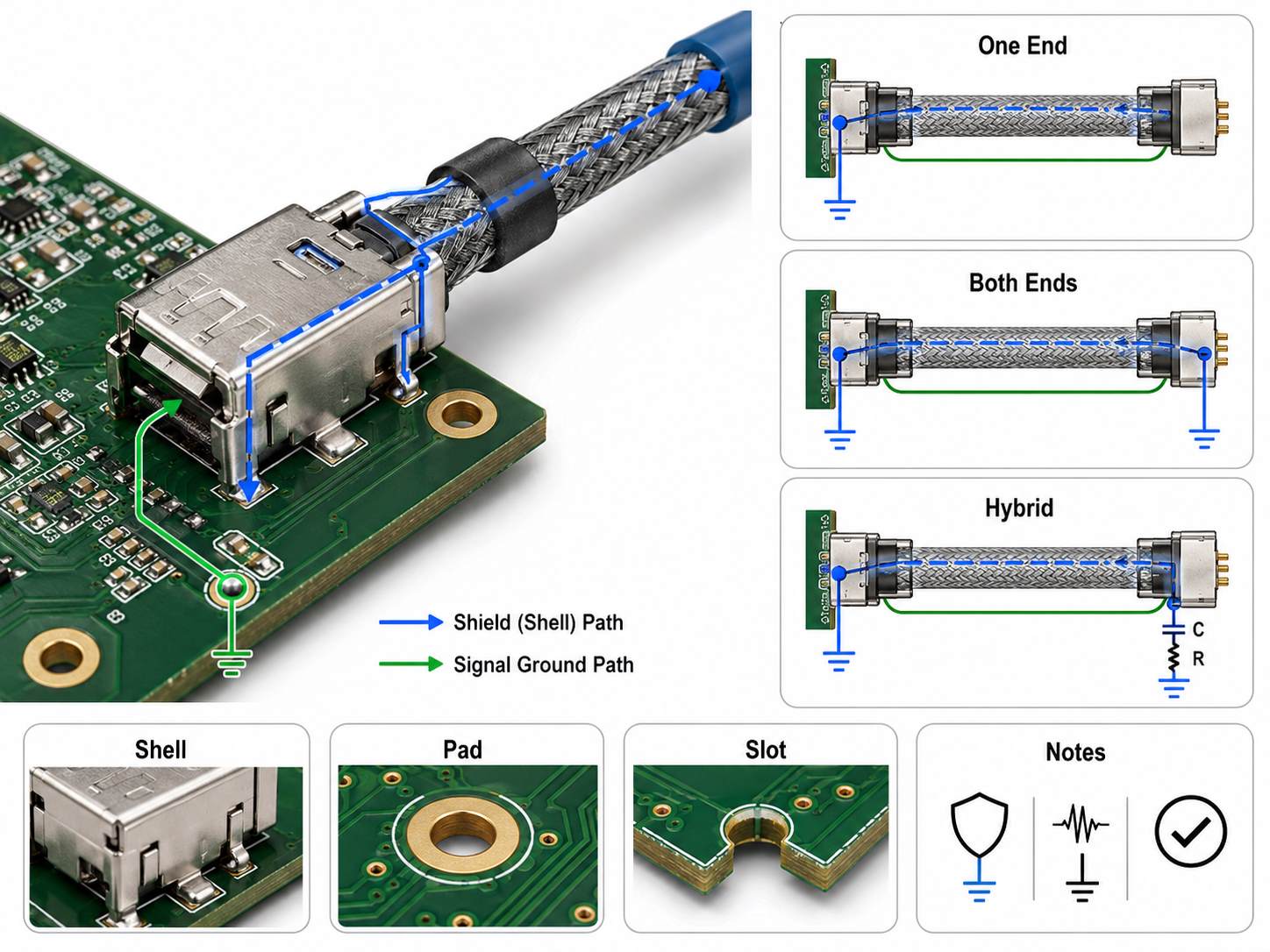
Cable Shield Grounding: One End or Both Ends?
Many searches around GND shielding are really about cable shield grounding. Engineers often ask whether a cable shield should be connected to GND at one end, both ends, or through a hybrid connection.
There is no single answer for every product.
| Method | Common Use |
|---|---|
| One-end grounding | Helps reduce low-frequency ground loop risk |
| Both-end grounding | Often used for high-frequency shielding paths |
| Hybrid grounding | Uses components or chassis strategy |
| Floating shield | Usually needs careful review |
For PCB and PCBA projects, the board must match the customer’s grounding method. If the cable shield connects to a connector shell, shield pad, chassis point, or mounting structure, the PCB files should make that clear.
Important manufacturing points include connector footprint accuracy, plated slot quality, solderability of shell pads, mechanical fit, and clear assembly notes.
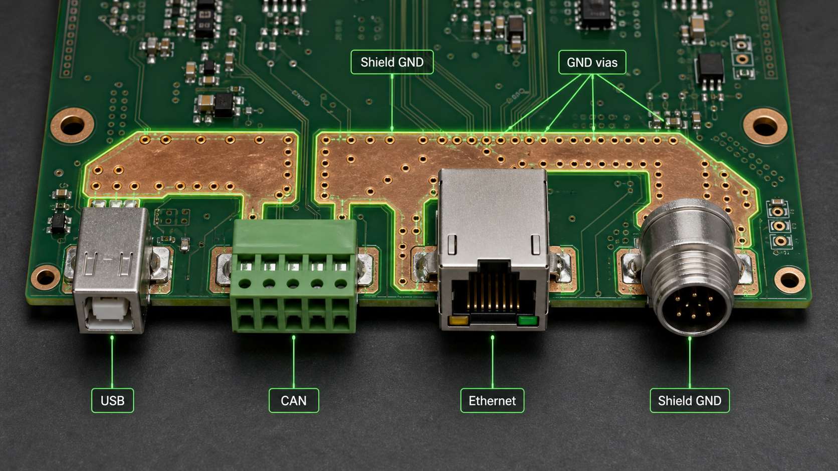
USB, CAN, and Connector Shield GND Notes
USB, CAN, Ethernet, and industrial connectors often bring GND shielding questions into PCB projects. The customer may specify how shield GND, signal GND, chassis ground, or enclosure contact should be handled.
For example:
- USB connector shells may need shield pads and controlled grounding strategy
- CAN interfaces may involve cable shield or chassis connection notes
- Ethernet connectors may have shield pins, magnetics, or chassis-related requirements
- Industrial modules may need enclosure contact or mounting-hole grounding
- Sensor boards may need shielded cable termination near the connector
The PCB manufacturer should not change these connections without approval. However, the manufacturer should check whether the connector shell pads, mounting holes, copper clearances, solder mask openings, and plating requirements are clear before production.
This is where DFM review is useful. It helps catch details before SMT, not after the first prototype fails inspection.
Ground Planes, Guard Traces, and Shielding Vias
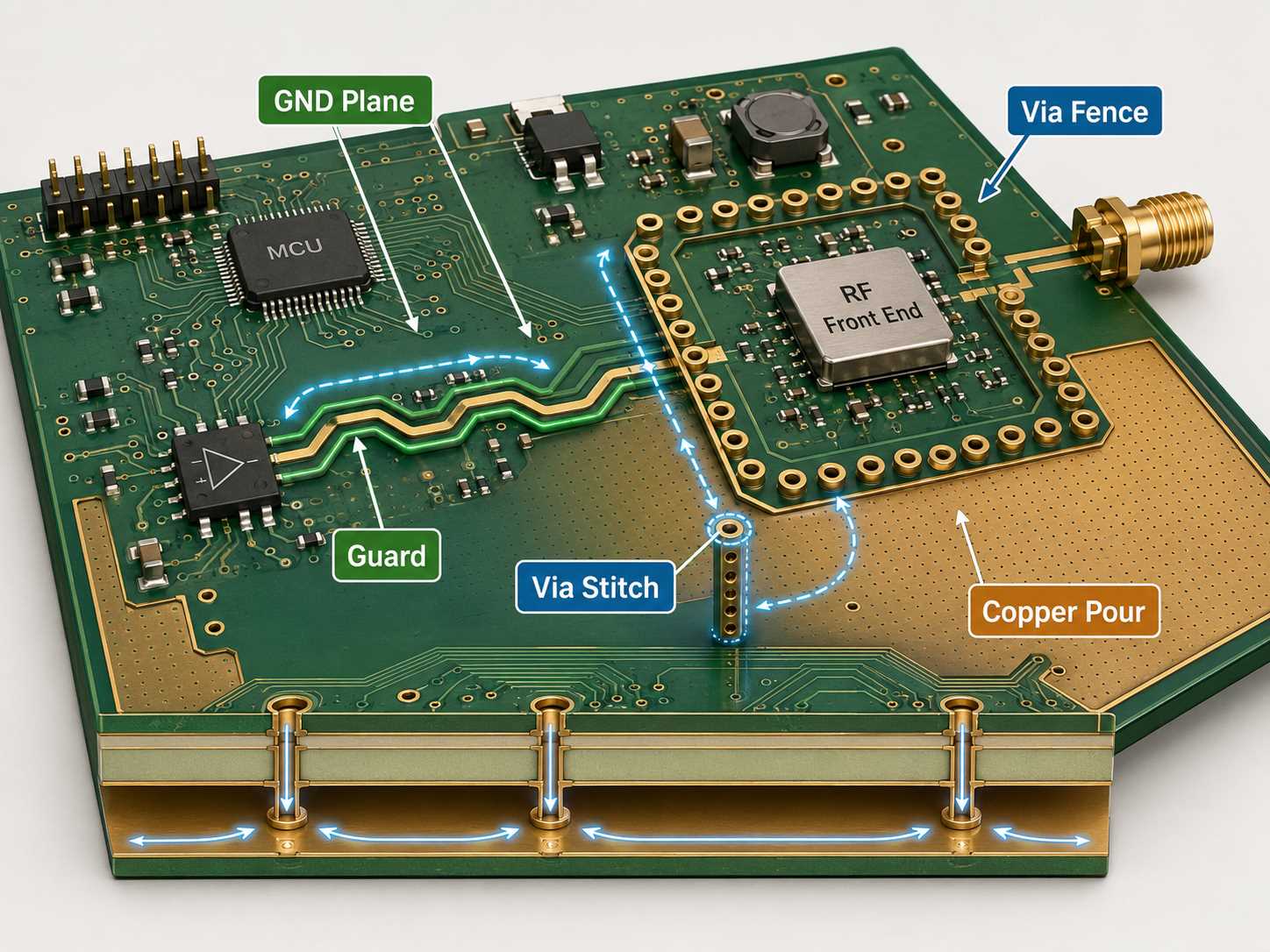
GND shielding is usually more effective when several layout details work together.
- Ground planes: A solid GND plane gives signals a stable return path and helps reduce loop area.
- Guard traces: Guard traces are often used around sensitive analog or high-impedance signals. They must be connected correctly to the intended reference.
- Shielding vias: Via stitching can connect ground copper between layers and help reduce gaps in shielding structures.
- Via fences: For RF or noisy areas, via fences may help define a boundary, but the spacing and placement should follow the customer’s RF/layout requirements.
- Copper pours: Copper pours should not create isolated copper islands or unexpected coupling paths.
For manufacturing, these details affect drilling, plating, solder mask, impedance, copper balance, and inspection. A shielding layout that looks good in CAD still needs to be manufacturable.
GND Shielding Checks Before PCB Manufacturing
Before a GND shielding PCB moves into production, EBest Circuit focuses on whether the files, stackup, and assembly requirements are clear enough to build.
| Check Item | What We Review |
|---|---|
| Gerber and ODB++ | Copper, mask, drill, outline |
| Stackup | Layer order and reference planes |
| Impedance notes | Trace width and dielectric control |
| Shield pads | Connector and shell solder areas |
| Via structure | Stitching, grounding, filled vias |
| Copper spacing | Clearance and manufacturability |
| Assembly notes | Shield cans, connectors, grounding points |
| Testing notes | Electrical and functional requirements |
This review is especially important for prototype and small-batch projects, because early mistakes can affect EMI testing, connector reliability, SMT yield, and project schedule.
PCBA Shielding and Assembly Quality Control
GND shielding does not end when the bare PCB is fabricated. Many shielding requirements become visible during assembly.
For PCBA projects, EBest Circuit checks:
- Shield can footprint and soldering area
- Connector shell solder joints
- SMT placement around shielded areas
- Solder mask openings near grounding pads
- Cleanliness around connectors and RF areas
- AOI inspection after SMT
- X-Ray inspection when BGA or hidden joints are involved
- Functional test coordination when required
If the board includes a shielding can, the soldering process must support reliable contact. If the board has connector shield pads, the shell must sit correctly. If the product uses conformal coating, potting, or enclosure grounding later, those process notes should be reviewed before assembly.
When shielding covers, connector shell grounding, or board-level shielding structures are involved, the manufacturing review should also consider solderability, grounding contact, mask openings, and assembly stability. These points are also important in an EMI shield PCB project.
A small grounding or shielding detail can become expensive if it is discovered after SMT. That is why EBest Circuit keeps PCB fabrication and PCBA assembly notes in the same review flow.
GND Shielding Case Study at EBest Circuit
A U.S. customer developed an industrial IoT wireless module that required stable signal transmission, controlled impedance, and careful grounding around connector and communication areas. The customer supplied the approved PCB layout and specification files, and EBest Circuit reviewed the manufacturing path before production.
Project profile
- 6-layer FR4 PCB
- IT180 material, Isola 370HR or equivalent
- Outer copper 1oz, inner copper 0.5oz
- Finished thickness 1.6mm +/-10%
- ENIG, Au 1u”
- Green solder mask, white silkscreen
- Differential impedance requirement
- Bare PCB factory panelization
- Production files confirmed by customer before manufacturing
Main risks
- Differential signals needed stable impedance control
- GND reference layers had to match the approved stackup
- Connector and shield-related pads needed clear solder mask definition
- Wireless and communication areas could not be treated like a simple FR4 board
- Production files had to be confirmed before fabrication
EBest Circuit’s support
- Reviewed stackup and impedance notes before production
- Checked copper thickness, dielectric structure, and reference layers
- Confirmed panelization before manufacturing
- Protected the customer’s approved GND and shielding intent in fabrication
- Prepared production data for customer confirmation
- Supported the project from PCB fabrication toward assembly readiness
For this type of project, the value is not that the factory “redesigns” the shielding strategy. The value is that the approved engineering intent is not lost during stackup review, fabrication, panelization, surface finish, and PCBA preparation.
FAQs about GND Shielding
1. What is GND shielding in PCB layout?
GND shielding is the use of ground planes, guard traces, via stitching, shield pads, connector grounding, or shielding structures to reduce noise coupling and support EMI control.
2. Is shield GND the same as signal GND?
Not always. Shield GND may connect to chassis, connector shells, cable shields, or enclosure grounding. Signal GND is usually the circuit reference. The connection method should follow the customer’s design.
3. Should a cable shield connect to GND at one end or both ends?
It depends on frequency, cable length, product structure, EMC requirements, and system grounding. One-end, both-end, and hybrid grounding can all be valid in different cases.
4. Does GND shielding replace a metal shield can?
No. Ground planes, shield GND, and shielding cans solve different parts of the EMI problem. Some products use only PCB-level shielding, while others need a shield can or metal enclosure.
5. What files should I send for a GND shielding PCB project?
Please send Gerber or ODB++ files, stackup, PCB drawing, impedance notes, BOM, placement file, assembly notes, connector datasheets, and any shielding or grounding requirements.
If your PCB or PCBA project includes GND shielding, shield GND, cable shield grounding, connector shell grounding, RF areas, high-speed signals, or EMI-related concerns, please contact sales@bestpcbs.com. EBest Circuit’s engineering team can help review the manufacturing and assembly path before production starts.
You may also like






Tags: gnd shielding, PCBA Shielding, Shield GND