PCB manufacturing PCB manufacturing
Home > Blog

Surface Mount Resistor Guide: Sizes, Codes, Types & Values

September 9th, 2026

A surface mount resistor is a compact resistor mounted directly onto PCB pads and assembled using surface mount technology. Common packages range from tiny 01005 and 0201 parts to larger 1206, 2010, and 2512 resistors used where more power or board space is available.

Selecting the right part involves more than resistance value. Engineers also need to consider resistor type, package size, tolerance, power rating, working voltage, TCR, and markings. This guide explains the most common surface mount resistor sizes, types, codes, and values, then shows how to choose one for a PCB.
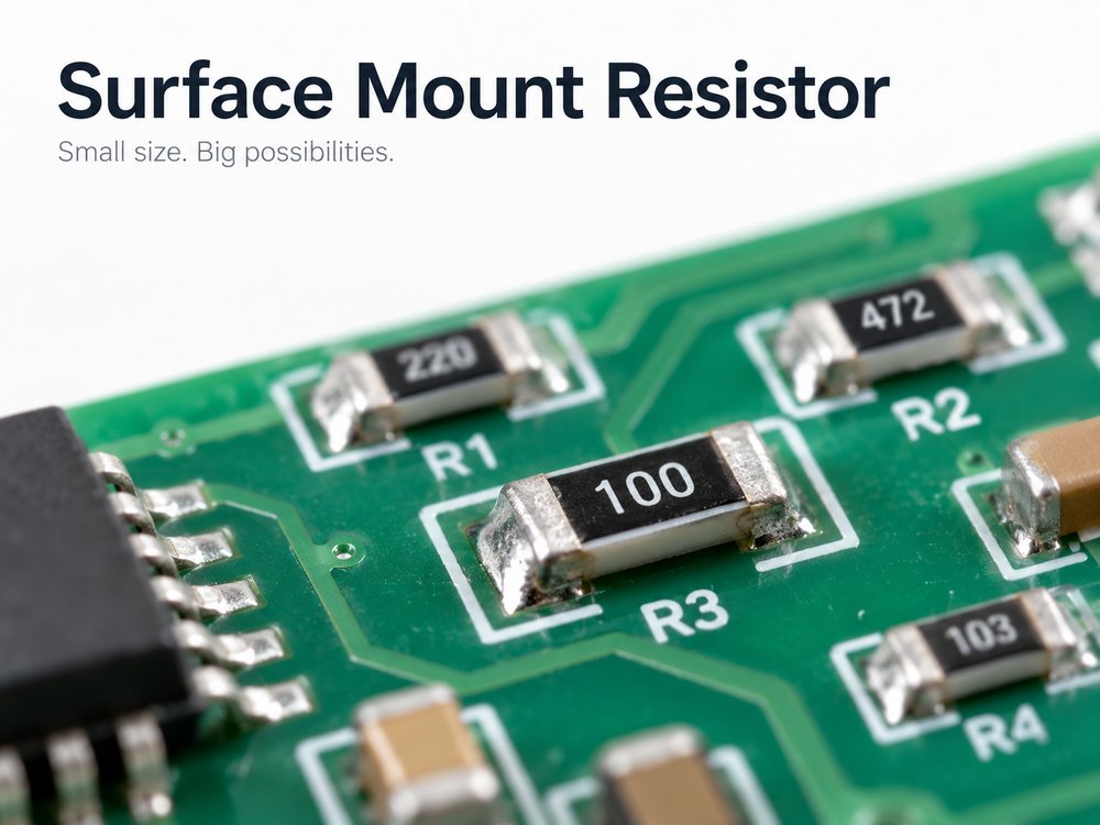
Surface mount resistor mounted on a printed circuit board

What Is a Surface Mount Resistor?

A surface mount resistor is a resistor designed to sit directly on conductive pads on the surface of a PCB. It does not use long leads passing through drilled holes like a through-hole resistor.

Other names commonly used for the same component include:

  • SMD resistor
  • chip resistor
  • surface mount chip resistor
  • SMT resistor

SMD means surface-mount device, while SMT refers to the process used to assemble surface-mount components.

A typical chip resistor contains:

  • a ceramic substrate
  • a resistive layer
  • metal terminal electrodes
  • a protective coating

During PCB assembly, solder paste is printed on the pads, the resistor is placed by pick-and-place equipment, and the joint is formed during reflow soldering.

The surface mount resistor symbol on a schematic is normally the same standard resistor symbol used for a through-hole part. Its reference designator is usually R, such as R1 or R24. Package information such as 0603 or 0805 is defined in the PCB footprint rather than the schematic symbol.

What Are the Main Surface Mount Resistor Types?

The main surface mount resistor types differ in resistive material, precision, temperature stability, current capability, and cost.
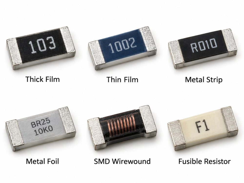
Comparison of thick film, thin film, metal strip, metal foil, wirewound and fusible surface mount resistor types
Type Main Characteristic Common Use
Thick film Cost-effective and widely available General PCB circuits
Thin film High precision and low TCR Analog and measurement circuits
Metal strip Very low resistance Current sensing
Metal foil High stability and accuracy Precision electronics
SMD wirewound Higher power and pulse capability Power circuits
Fusible Designed to open under overload Circuit protection

Thick-film resistors

These are the standard choice for many PCB designs. They cover a broad resistance range and are readily available in packages such as 0402, 0603, 0805, and 1206.

Typical uses include:

  • pull-up and pull-down networks
  • LED current limiting
  • bias circuits
  • general signal conditioning

Thin-film resistors

Thin-film parts are used when tighter tolerance and lower temperature coefficient are required. They are common in:

  • precision amplifiers
  • sensor interfaces
  • measurement circuits
  • accurate voltage dividers

Metal strip resistors

Metal strip parts are mainly used for low-resistance current sensing. Values may be measured in milliohms rather than ohms, making them useful in battery systems, power supplies, motor drives, and power converters.

The resistor type should therefore match the electrical requirement. Two resistors with the same resistance and package size can have very different tolerance, TCR, pulse capability, and stability.

What Surface Mount Resistor Sizes Are Common?

Common surface mount resistor sizes include 0201, 0402, 0603, 0805, 1206, 2010, and 2512. Smaller packages reduce PCB area, while larger packages generally offer higher power capability and easier handling.
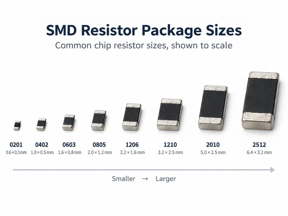
Surface mount resistor size comparison from 0201 to 2512 packages
Imperial Size Metric Code Approx. Size (mm) Typical Conventional Power*
01005 0402 0.4 × 0.2 ~0.03 W
0201 0603 0.6 × 0.3 ~0.05 W
0402 1005 1.0 × 0.5 ~0.063 W
0603 1608 1.6 × 0.8 ~0.10 W
0805 2012 2.0 × 1.25 ~0.125 W
1206 3216 3.2 × 1.6 ~0.25 W
1210 3225 3.2 × 2.5 ~0.5 W
2010 5025 5.0 × 2.5 ~0.75 W
2512 6332 6.3 × 3.2 ~1 W

*These are common reference ratings rather than universal specifications. The exact rating must be checked in the resistor manufacturer’s datasheet.

The imperial package code approximately represents component length and width in hundredths of an inch. For example:

  • 0603 ≈ 0.06 × 0.03 inch
  • 0805 ≈ 0.08 × 0.05 inch
  • 1206 ≈ 0.12 × 0.06 inch

Metric and imperial codes should not be confused. An imperial 0603 package, for example, corresponds to metric 1608 rather than metric 0603.

Package size also affects manufacturability. Moving from 0805 or 0603 to 0402, 0201, or smaller parts generally requires tighter control of:

The smallest surface mount resistor is therefore not automatically the best choice. Use a smaller package when PCB density requires it, not simply because the package is available.

How Do You Read Surface Mount Resistor Codes and Markings?

Surface mount resistor markings use numbers and letters to represent resistance because the component body is too small for traditional color bands. The most common surface mount resistor code systems are 3-digit codes, 4-digit codes, R notation, and EIA-96.
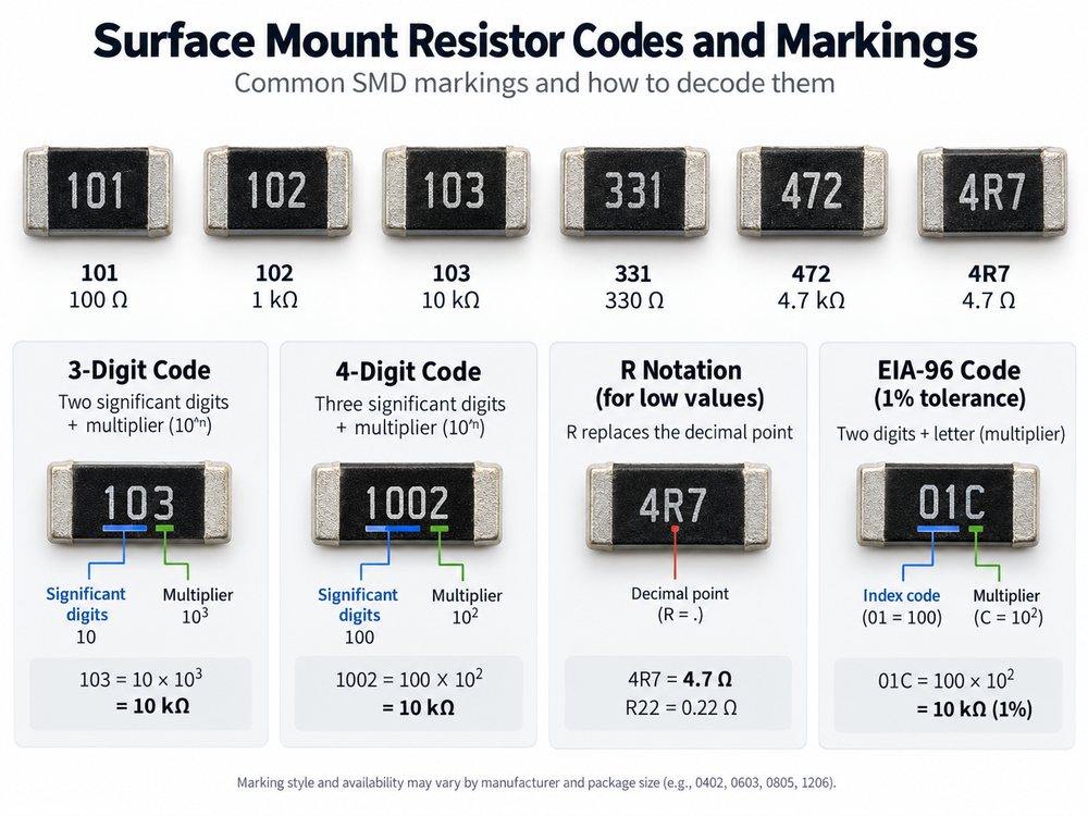
Surface mount resistor codes and markings showing 3-digit, 4-digit, R notation and EIA-96 examples

3-digit surface mount resistor code

The first two digits are significant figures. The third digit tells you how many zeros to add.

Code Calculation Value
101 10 × 101 100 Ω
102 10 × 102 1 kΩ
103 10 × 103 10 kΩ
331 33 × 101 330 Ω
472 47 × 102 4.7 kΩ

4-digit surface mount resistor code

The first three digits are significant figures and the fourth digit is the multiplier.

Examples:

  • 1001 = 100 × 101 = 1 kΩ
  • 4701 = 470 × 101 = 4.7 kΩ
  • 1002 = 100 × 102 = 10 kΩ
  • 4702 = 470 × 102 = 47 kΩ

Four-digit markings are often found on tighter-tolerance resistor series.

R notation

For low resistance values, R is used as the decimal point.

Examples:

  • R10 = 0.10 Ω
  • R47 = 0.47 Ω
  • 2R2 = 2.2 Ω
  • 4R7 = 4.7 Ω

EIA-96 resistor markings

EIA-96 uses two digits followed by a letter. The two-digit number refers to one of 96 standard base values, while the letter gives the multiplier.

Because the number is a lookup code rather than the resistance itself, an EIA-96 surface mount resistor code chart or calculator is usually the quickest way to decode it.

Unmarked surface mount resistors

01005, 0201, and some other small resistors may have no readable top marking. Their value should be identified using:

Appearance alone is not enough because different values can use identical packages.

Surface Mount Resistor Values: What Do 100, 101, 102 and 103 Mean?

For a standard 3-digit surface mount resistor marking, the first two digits give the significant value and the third digit gives the multiplier.
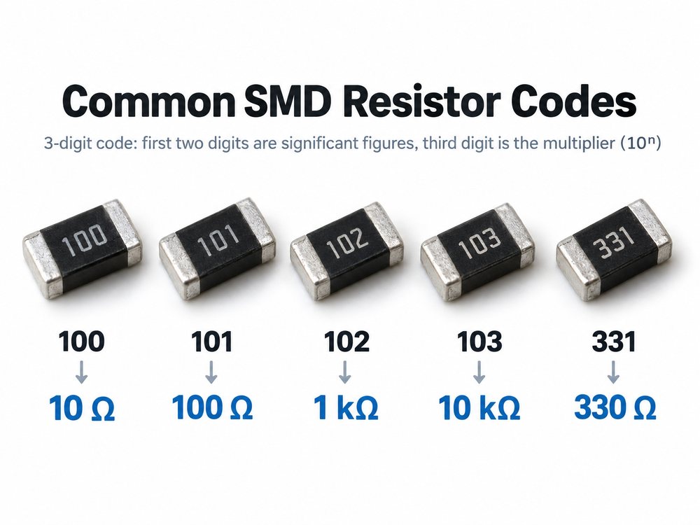
Common SMD resistor code values including 100, 101, 102, 103 and 331
Surface Mount Resistor Code Resistance Value
100 10 Ω
101 100 Ω
102 1 kΩ
103 10 kΩ
221 220 Ω
331 330 Ω
472 4.7 kΩ
104 100 kΩ

The code 100 is particularly easy to misread.

100 means:

10 × 100 = 10 Ω

It does not normally mean 100 Ω.

A 100 ohm surface mount resistor commonly uses the code 101:

10 × 101 = 100 Ω

Other common examples are:

  • 102 surface mount resistor = 1 kΩ
  • 103 surface mount resistor = 10 kΩ
  • 331 surface mount resistor = 330 Ω
  • 472 surface mount resistor = 4.7 kΩ

For example, a standard 330 ohm 0805 surface mount resistor may carry the marking 331 when that resistor series uses body markings.

How Do You Choose the Right Surface Mount Resistor for a PCB?

Choose a surface mount resistor by checking the required resistance first, then tolerance, power, voltage, temperature behavior, pulse load, and package size.

The main specifications are:

  • Resistance: Match the nominal value required by the circuit.
  • Tolerance: ±5% and ±1% are common; precision designs may need ±0.5%, ±0.1%, or tighter.
  • Power rating: Calculate actual dissipation and leave suitable operating margin.
  • Working voltage: Check this separately from wattage, especially in high-voltage circuits.
  • TCR: Use a lower temperature coefficient when resistance stability over temperature matters.
  • Pulse rating: Check surge capability for startup, switching, discharge, and transient loads.
  • Package: Select a size that meets both electrical and PCB space requirements.
  • Availability: Check whether the exact series is practical to source throughout production.

Resistor power can be estimated using:

P = I2R

P = V2 / R

Package wattage should not be treated as a universal limit. The usable power also depends on the exact resistor series, ambient temperature, PCB copper area, and manufacturer derating curve.

Package selection also affects assembly. An electrically suitable 0201 resistor may be unnecessary if an 0603 fits comfortably and the product does not require extreme component density.

For production PCBs, the preferred package is usually the smallest size that meets the electrical and layout requirements without adding unnecessary assembly difficulty.

Surface Mount Resistor vs Through-Hole Resistor: Which Should You Use?

The surface mount resistor vs through hole choice depends on assembly method, PCB area, mechanical needs, and power requirements. A surface mount resistor is usually preferred for compact and automated PCB assembly, while a through-hole resistor remains useful when easy manual handling, mechanical retention, or certain high-power requirements matter more.
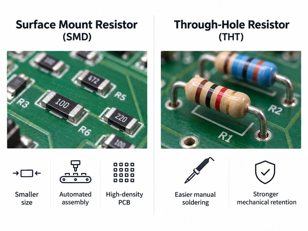
Surface mount resistor versus through-hole resistor comparison on printed circuit boards
Factor Surface Mount Resistor Through-Hole Resistor
PCB area Smaller Larger
Automated assembly Well suited Less efficient
Component density Higher Lower
Lead inductance Lower Higher
Manual soldering More difficult Easier
Mechanical retention Lower Stronger
Rework Harder at small sizes Usually easier
High-density PCB Preferred Less suitable

Choose a surface mount resistor when the design prioritizes:

  • compact PCB size
  • automated SMT production
  • high component density
  • short electrical paths
  • double-sided component placement

Choose a through-hole resistor when the design benefits more from:

  • manual assembly
  • straightforward repair
  • stronger mechanical retention
  • large leaded power components
  • simple prototype construction

For most modern volume-produced PCB assemblies, surface mount resistors are the default choice.

FAQs About Surface Mount Resistors

1. What does 102 mean on a surface mount resistor?

102 means 1 kΩ. The first two digits are 10, and the third digit adds two zeros: 10 × 100 = 1,000 Ω.

2. What does 103 mean on a surface mount resistor?

103 means 10 kΩ: 10 × 1,000 = 10,000 Ω.

3. Is an 0805 resistor always 1/8 watt?

No. Around 0.125 W is a common conventional rating, but the actual rating depends on the resistor series, construction, temperature, and manufacturer.

4. What is the smallest surface mount resistor size?

01005-class and smaller specialized resistors are available. The smallest practical package for a PCB depends on placement capability, stencil printing, inspection, rework, and required production yield.

5. Why do some surface mount resistors have no markings?

Small packages may not have enough body area for readable markings. Their resistance should be verified from the BOM, reel label, manufacturer part number, or measurement.

6. Is an SMD resistor the same as an SMT resistor?

In everyday use, the terms often refer to the same type of component. Technically, SMD means surface-mount device, while SMT is the manufacturing technology used to assemble it.

If you are preparing a PCB or PCBA project and need support with component package selection, SMT manufacturability, stencil design, or assembly planning, send your Gerber files, BOM, and assembly requirements to sales@bestpcbs.com
You may also like

Reflow Process Soldering: SMT Steps, Temperature Profile & Defects

September 9th, 2026

The reflow process soldering method is an SMT assembly process where solder paste is printed on PCB pads, components are placed, and the assembly passes through a controlled oven profile. The main stages are preheat, soak, reflow and cooling. Reliable results depend on paste volume, placement accuracy, peak temperature, time above liquidus, cooling rate and inspection.

The reflow soldering process is simple in principle, but reliable results depend on more than reaching the solder’s melting point. Paste volume, component placement, PCB thermal mass, oven settings, peak temperature, time above liquidus, and cooling rate all influence the final joint. A profile that works for a small two-layer PCB may therefore be unsuitable for a dense multilayer assembly with BGAs, large copper planes, or mixed component sizes.

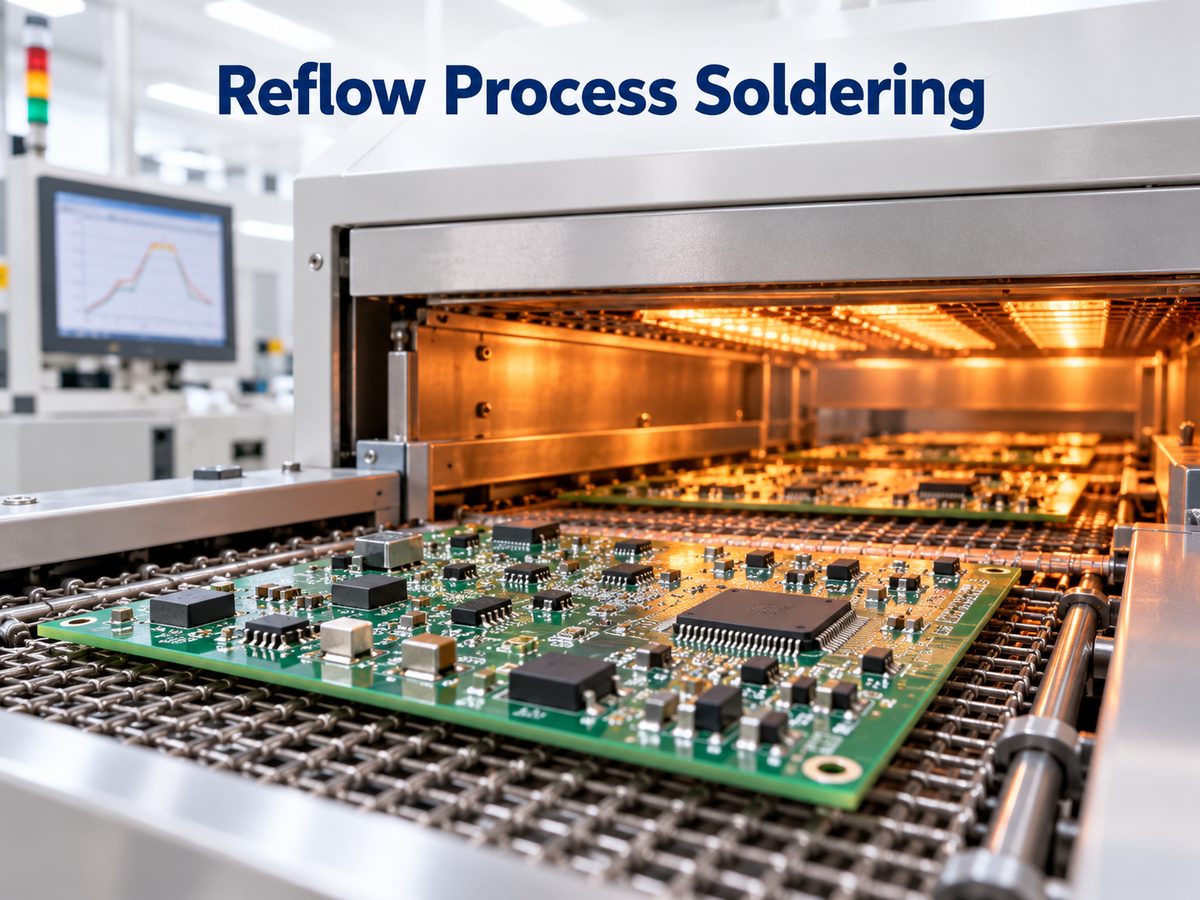
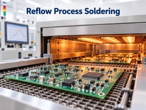
Reflow process soldering line with a populated PCB moving through a reflow oven

What Is Reflow Process Soldering in Electronics Manufacturing?

Reflow process soldering is the standard method used to attach most surface-mount components to printed circuit boards. Solder paste is first printed onto PCB pads, components are placed into the paste, and the assembly then travels through a reflow oven. Controlled heating activates the flux, melts the solder alloy, forms the joints, and finally cools them into a stable connection.

Before heating, the solder paste holds the components in position. As the board enters the hotter sections of the reflow oven, the flux activates and removes oxides from the surfaces being joined. Once the solder alloy passes its liquidus temperature, it melts and wets the component terminals and PCB pads. Cooling then solidifies the solder into permanent electrical and mechanical joints.

Reflow is especially suitable for modern PCB assembly because hundreds or thousands of SMT joints can be processed during the same oven cycle. It also supports fine-pitch ICs, QFNs, BGAs, chip resistors, capacitors, and other high-density components that would be difficult to solder individually.

The process is commonly used for:

  • Consumer and industrial electronics
  • Automotive control boards
  • Telecom and networking equipment
  • Medical electronics
  • Power electronics
  • IoT devices
  • High-density computing hardware

How Does the Reflow Soldering Process Work Step by Step?

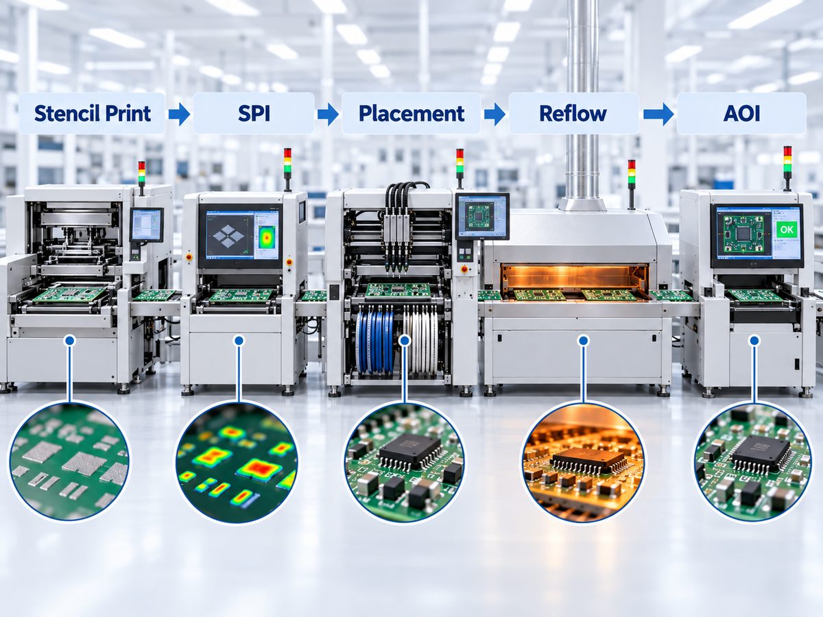
The complete SMT reflow soldering process includes several operations before and after the PCB enters the oven. Treating the oven itself as the entire process overlooks many of the variables that determine solder-joint quality. A PCB reflow soldering process must therefore control printing, placement, heating, cooling, and inspection as one connected workflow.

SMT reflow soldering workflow showing stencil printing, SPI, placement, reflow and AOI

1. PCB and stencil preparation

The PCB surface and stencil must be clean and compatible with the selected solder paste. Stencil thickness and aperture design determine how much paste is transferred onto each pad.

Fine-pitch packages normally need tighter control of aperture geometry than larger passive components.

2. Solder paste printing

A stencil printer pushes solder paste through the stencil apertures and deposits it onto exposed PCB pads.

Paste height, area, volume, alignment, and release consistency matter. Too much paste can encourage bridging or solder balls, while insufficient deposits can cause weak or open joints.

3. Solder Paste Inspection

SPI equipment checks the printed deposits before components are placed. This step can identify:

  • Insufficient paste
  • Excess paste
  • Offset deposits
  • Poor stencil release
  • Inconsistent paste volume

Finding these problems before placement and reflow is generally more efficient than diagnosing solder defects afterward.

4. Component placement

Pick-and-place equipment positions SMT components onto the printed solder paste. Placement accuracy becomes particularly important for fine-pitch ICs, small chip components, BGAs, QFNs, and boards with high component density.

Surface tension during reflow can correct small placement offsets, but it cannot compensate for large errors, incorrect polarity, severe rotation, or inappropriate pad and paste geometry.

5. Reflow soldering

The populated PCB travels through the reflow oven on a conveyor. Multiple heating zones create a controlled temperature profile that gradually heats the assembly, activates the flux, melts the alloy, and then cools the joints.

6. Post-reflow inspection

After cooling, AOI can detect visible defects such as bridging, component shift, polarity errors, and missing components. For BGAs, QFNs, and other packages with hidden joints, X-ray inspection may be required.

What Happens During the Four Reflow Oven Stages?

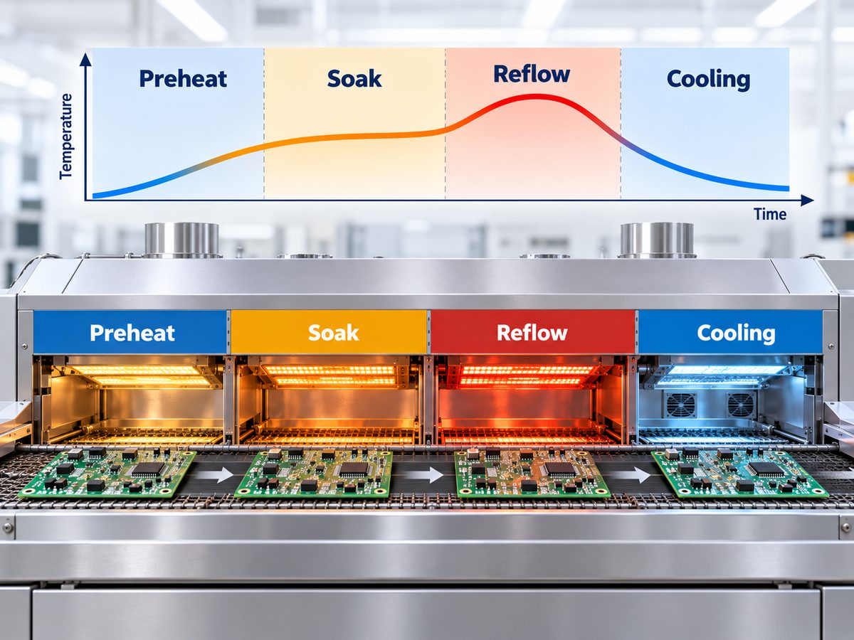
The reflow oven soldering process is typically divided into preheat, soak, reflow, and cooling. Each stage has a different thermal function.

Four reflow oven stages and temperature profile: preheat, soak, reflow and cooling
Reflow Stage Main Purpose Main Control Point
Preheat Raise PCB temperature gradually Ramp rate
Soak Reduce thermal differences and activate flux Time and temperature
Reflow Melt solder and form the joint Peak temperature and TAL
Cooling Solidify the solder joint Cooling rate

Preheat

During preheating, the PCB temperature rises gradually from ambient temperature. Excessively rapid heating can increase thermal stress, solder spattering, component damage, and temperature differences across the assembly.

For many solder paste systems, an average heating rate around 0.5–2.5°C/s can serve as a practical starting window, although the paste manufacturer’s recommended profile should take priority.

Soak

The soak stage allows different areas of the PCB to approach a more uniform temperature while the flux continues to activate.

This becomes useful on boards containing both high-thermal-mass and low-thermal-mass areas. Large copper planes, connectors, shields, BGAs, and power devices can heat more slowly than small passive components.

The exact soak range is paste-dependent rather than universal.

Reflow

During this stage, the solder passes its liquidus temperature and wets the PCB pads and component terminations.

Two parameters are especially important:

  • Peak temperature
  • Time Above Liquidus (TAL)

Too little thermal energy may result in incomplete wetting. Excessive temperature or excessive TAL can stress components, accelerate intermetallic growth, and degrade flux performance.

Cooling

Once the solder joint has formed, the PCB moves through the cooling zones. Controlled cooling solidifies the alloy and establishes its final microstructure.

Very slow cooling can affect joint structure, while excessively fast cooling may introduce thermal stress. The acceptable range should therefore be treated as part of the verified reflow profile rather than an isolated oven setting.

What Is Reflow Solder Paste Made Of?

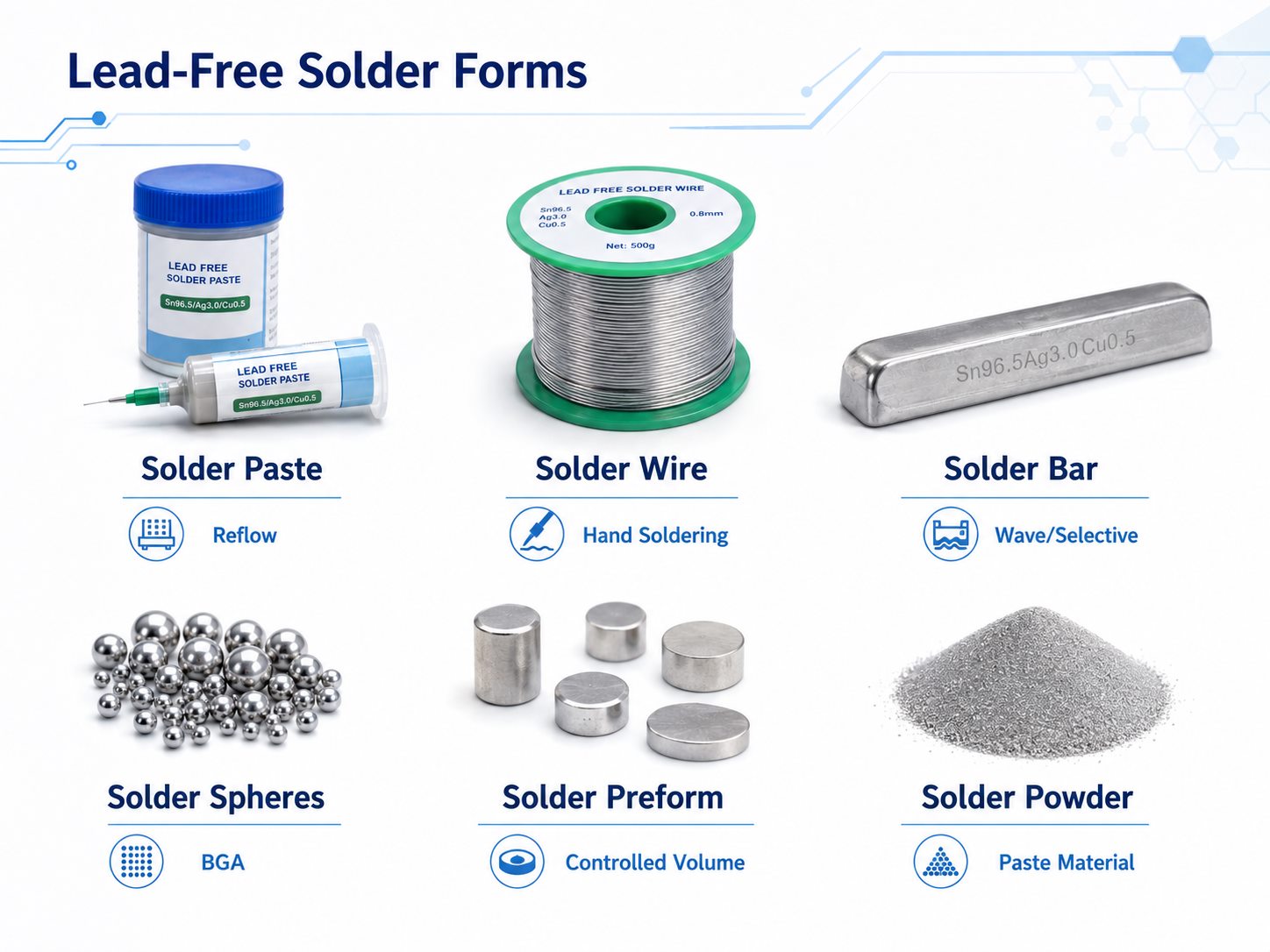
Reflow solder paste is a printable mixture of metal alloy powder and flux chemistry. It must remain stable enough for stencil printing, hold components during placement, and then perform correctly as temperature rises.

Typical solder paste contains:

  • Solder alloy powder: Forms the final metallic joint.
  • Flux: Removes surface oxides and assists wetting.
  • Activators: Improve the flux’s ability to clean solderable surfaces.
  • Solvents: Help control paste consistency and processing behavior.
  • Rheology modifiers: Control viscosity, slump, printing, and stencil release.

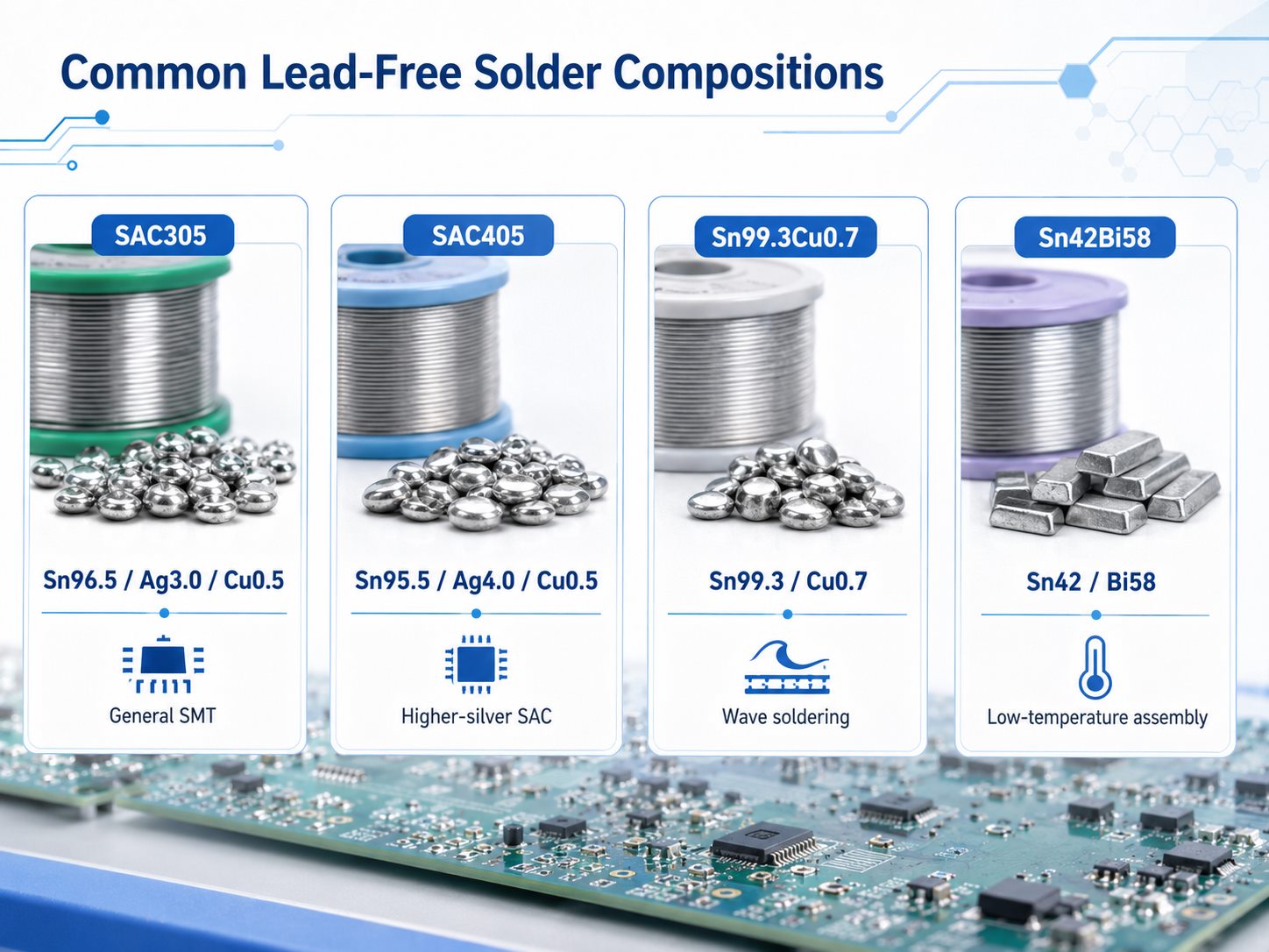
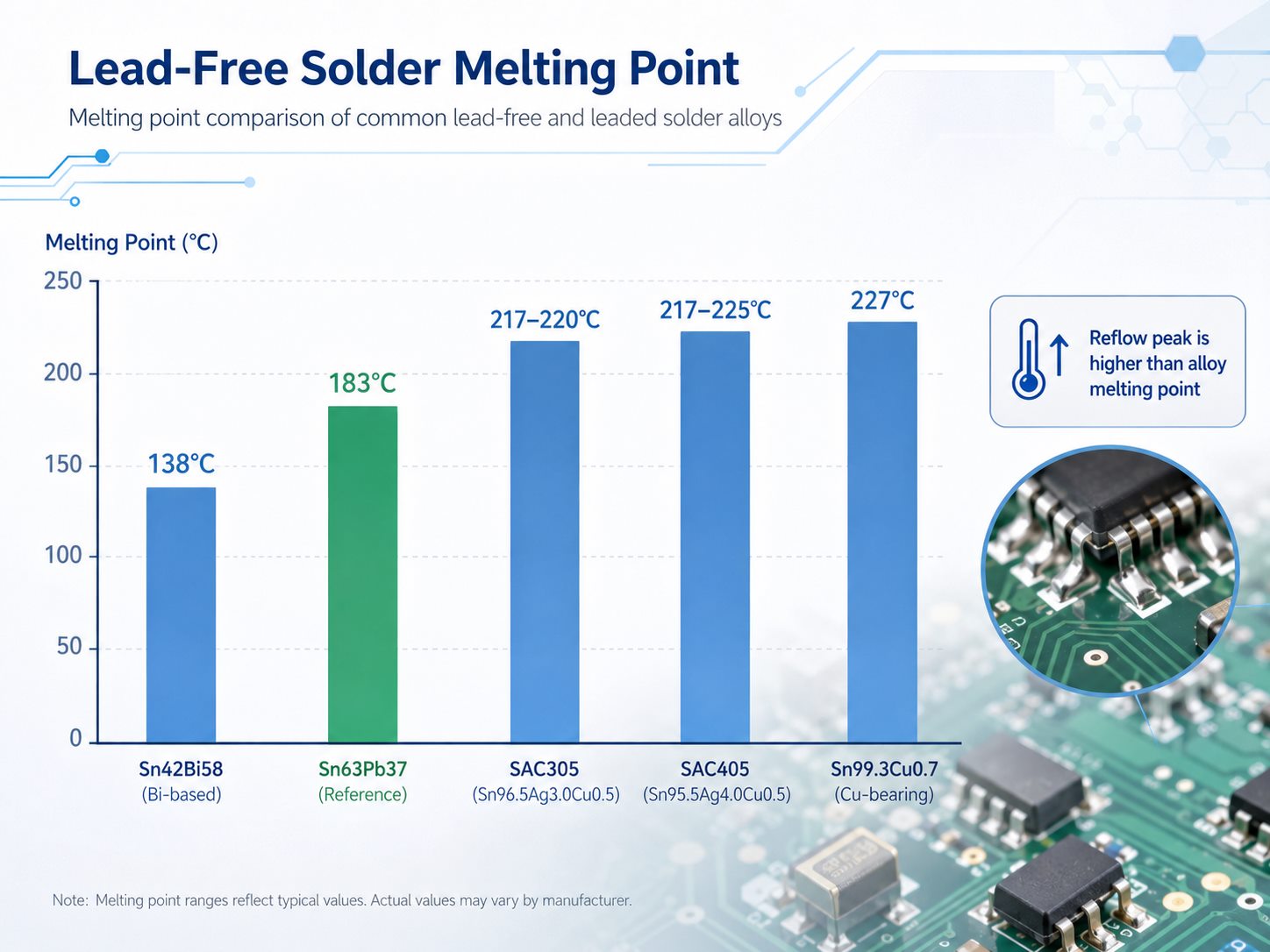
SAC305 is a widely used lead-free alloy containing approximately 96.5% tin, 3.0% silver, and 0.5% copper. Its liquidus temperature is around 217°C.

Sn63/Pb37, still used in some permitted legacy and high-reliability applications, is a eutectic alloy containing 63% tin and 37% lead with a melting point of 183°C.

Alloy selection alone is not enough. Powder size, flux classification, storage condition, stencil design, PCB finish, component termination, cleaning requirements, and process atmosphere can also affect printing and reflow performance.

What Temperature Profile Is Used for Reflow Soldering?

There is no single reflow soldering temperature profile that works for every PCB.

For lead-free SAC305 assemblies, peak temperature often falls in roughly the 230–260°C range, while the alloy liquidus is about 217°C. The exact profile must still follow the solder paste specification and the thermal behavior of the actual assembly.

A practical starting reference may look like this:

Parameter Typical SAC305 Starting Window
Average ramp rate About 0.5–2.5°C/s
Soak Paste-dependent; commonly around 140–170°C
Liquidus About 217°C
Time Above Liquidus About 30–100 s
Peak temperature About 230–260°C
Cooling rate Controlled according to paste and assembly requirements

For Sn63/Pb37, the thermal requirement is lower. The alloy melts at 183°C, with common peak reflow temperatures around 205–215°C for applicable solder systems.

These figures are useful starting points, not fixed production settings.

The final oven recipe should account for:

  • Solder paste manufacturer’s TDS
  • PCB thickness and layer count
  • Copper distribution
  • Component density
  • Large thermal-mass components
  • BGA and QFN packages
  • Temperature-sensitive components
  • Conveyor speed
  • Oven zone configuration
  • Air or nitrogen atmosphere

A thermocouple profiling run is therefore more reliable than setting the oven solely from a generic temperature chart. Thermocouples should be placed at representative hot and cold locations so the engineer can confirm that all critical joints remain inside the acceptable process window.

Two profile shapes are commonly encountered: Ramp-Soak-Spike (RSS) and Ramp-to-Spike (RTS). Neither is automatically better. Paste chemistry, board construction, voiding behavior, thermal gradients, and component mix determine which approach is more appropriate.

What Equipment Is Used in the Reflow Soldering Process?

Industrial reflow soldering is part of a complete SMT production line rather than a standalone oven operation.

Typical equipment includes:

  • Stencil printer
  • Solder paste inspection system
  • Pick-and-place machine
  • Multi-zone reflow oven
  • Thermal profiler and thermocouples
  • AOI system
  • X-ray inspection equipment when required

The multi-zone convection reflow oven is the central thermal-processing machine. Independent heating zones allow the line engineer to shape the PCB’s actual temperature curve rather than simply selecting one oven temperature.

Conveyor speed is equally important. A change in belt speed changes how long the PCB remains in each thermal region, which can alter soak duration, TAL, and peak temperature even when individual oven-zone setpoints remain unchanged.

Nitrogen reflow may be used when reduced oxidation or improved wetting is valuable. Vacuum reflow is used in more specialized applications where controlling solder voiding is particularly important. These processes add capability but are not mandatory for every PCBA.

What Are the Most Common Reflow Soldering Defects?

Reflow defects usually come from an interaction between printing, PCB design, component placement, material condition, and the thermal profile. Changing oven temperature alone will not solve every problem.

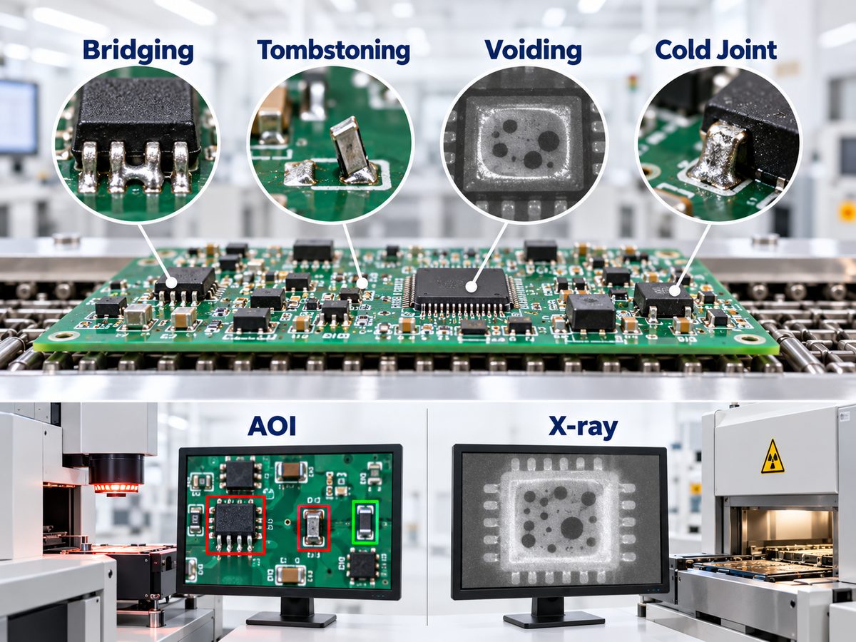
Common reflow soldering defects including bridging, tombstoning, voiding and cold joints with AOI and X-ray inspection
Defect Common Process Causes Typical Corrective Direction
Tombstoning Uneven heating, unequal paste deposits, pad imbalance Improve thermal balance and paste consistency
Solder bridging Excess paste, poor stencil design, placement offset Adjust aperture, paste volume and placement
Cold or poor joints Insufficient heat or TAL, poor wetting Verify profile and solderability
Voiding Flux outgassing, pad design, paste/profile interaction Optimize paste, aperture and profile
Solder balls Paste slump, rapid heating, contamination Review printing, paste handling and ramp rate
Head-in-pillow BGA warpage, oxidation, insufficient wetting Review component warpage and profile
Component shift Placement error or uneven wetting forces Check placement, pads and paste distribution

Tombstoning is a good example of why root-cause analysis matters. If one termination of a small passive component melts and wets earlier than the other, the resulting unbalanced surface tension can lift the component onto one end.

For BGA and QFN assemblies, visual inspection cannot evaluate hidden solder joints. X-ray inspection can reveal voiding, bridging, missing balls, alignment issues, and other defects underneath the package.

Reflow Soldering vs Wave Soldering: What Is the Difference?

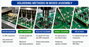
Reflow soldering is primarily associated with SMT components, while wave soldering is mainly used for through-hole components. The two processes also deliver solder in fundamentally different ways.

Comparison of reflow soldering for SMT and wave soldering for through-hole assembly
Factor Reflow Soldering Wave Soldering
Main component type SMT Through-hole
Solder source Printed solder paste Molten solder bath
Heating method Controlled reflow oven PCB passes over solder wave
Fine-pitch SMT Well suited Generally unsuitable
Typical production use SMT assembly THT assembly
Joint formation Paste melts on individual pads Exposed joints contact molten solder

Mixed-technology PCBAs may use both processes. SMT components can be reflowed first, followed by wave or selective soldering for through-hole components that cannot be processed during the SMT reflow stage.

The correct choice therefore depends less on which process is “better” and more on the component technology, PCB layout, heat sensitivity, production volume, and assembly sequence.

FAQs About Reflow Process Soldering

1. Which is the second stage in the reflow soldering process?

If the question refers to the four thermal stages inside a reflow oven, the second stage is the soak stage, following preheat. In a complete SMT manufacturing workflow, however, manufacturers may divide and number printing, SPI, placement, reflow, and inspection differently.

2. What temperature is used for reflow soldering?

For SAC305 lead-free solder, peak temperatures commonly fall within roughly 230–260°C, depending on the solder paste and assembly. Sn63/Pb37 uses a lower thermal profile and may peak around 205–215°C. The solder paste TDS and measured board profile should take priority over a generic peak-temperature value.

3. What is Time Above Liquidus in reflow soldering?

Time Above Liquidus, or TAL, is the period during which the solder joint remains hotter than the alloy’s liquidus temperature. It must be long enough to achieve suitable melting and wetting without subjecting the assembly to unnecessary thermal exposure.

For SAC305 processes, a range around 30–100 seconds may be encountered depending on the solder paste, although the correct value remains paste- and assembly-specific.

4. What solder paste is used for reflow soldering?

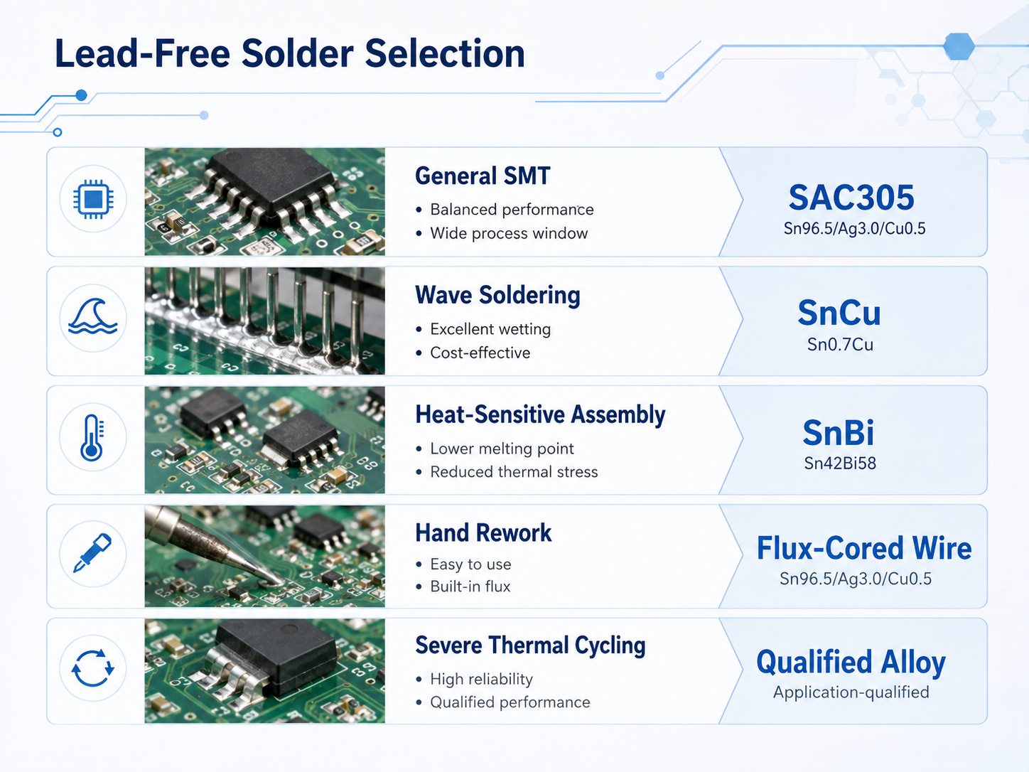
Lead-free SAC305 is widely used in current electronics assembly. Other alloys are selected for lower temperature, reliability, cost, regulatory, or application-specific requirements. The flux system and powder size must also match the PCB, stencil, component pitch, storage conditions, and cleaning process.

5. Can through-hole components be reflow soldered?

Some through-hole components can be assembled using pin-in-paste or intrusive reflow, where solder paste is printed around or into plated through-holes before the component is inserted and reflowed.

The component must tolerate the thermal profile, and sufficient solder volume must be provided to achieve acceptable barrel fill. For many conventional through-hole assemblies, wave or selective soldering remains more practical.

6. What is the difference between wave soldering and reflow soldering?

Reflow soldering heats deposited solder paste and is mainly used for SMT assembly. Wave soldering moves the underside of the PCB across a controlled wave of molten solder and is mainly used for through-hole assembly. Mixed PCBAs may use reflow for SMT first and wave or selective soldering afterward.

How Can EBest Circuit Support Your Reflow Soldering Project?

If you are preparing a PCB or PCBA project and need support with soldering process requirements, assembly manufacturability, or production planning, send your Gerber files, BOM, and assembly requirements to sales@bestpcbs.com. Our engineering team can review the project before production and help identify process conditions that may affect solder-joint quality, component reliability, or assembly yield.

You may also like

PCB and PCBA Manufacturer Israel: Top 5 Companies to Compare

September 8th, 2026

A search for PCB and PCBA manufacturer Israel usually begins with a practical goal: find one company that can turn released board data into working assemblies without forcing your team to manage a PCB factory, component suppliers and an assembly house separately. The right choice can shorten communication, make quotations easier to compare and prevent fabrication or sourcing decisions from disrupting assembly.

Israel offers established local PCB and electronics manufacturers, while overseas production gives eligible projects another combination of technology, capacity and cost. This guide compares five Israel-based companies, explains when local production matters and shows where EBest Circuit can support Israeli customers as a China-based PCB and PCBA manufacturer. EBest is not an Israeli manufacturer, so projects that require domestic production should use a qualified local route.

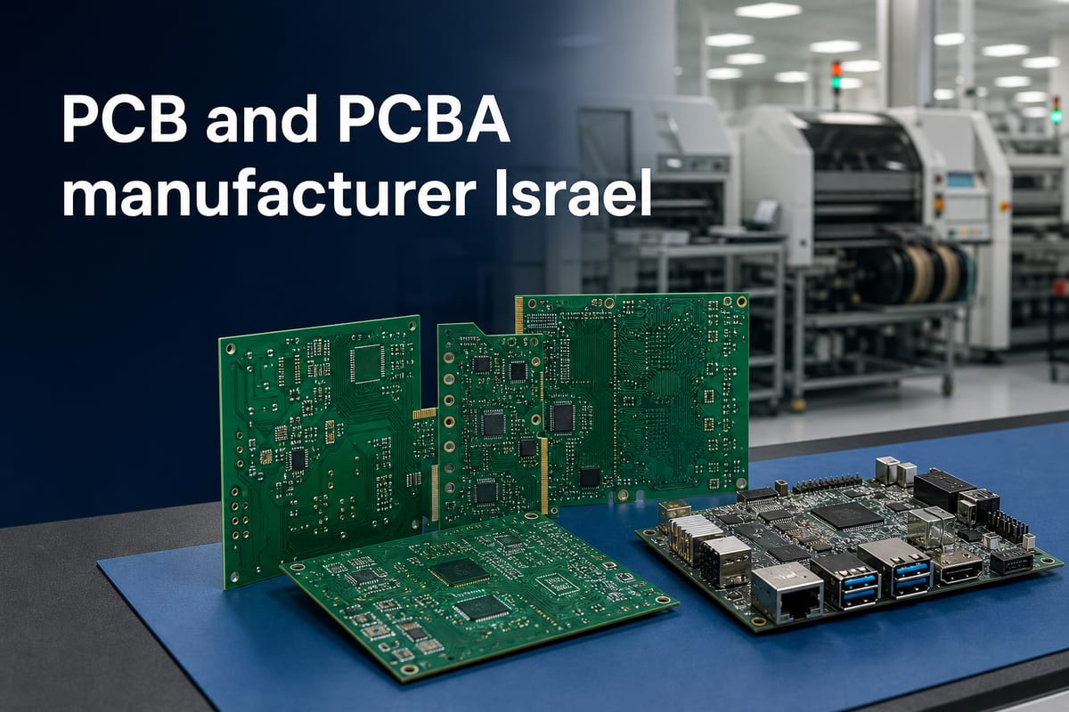
PCB and PCBA manufacturer Israel
PCB and PCBA manufacturing support for projects serving Israel.

What Can a PCB and PCBA Manufacturer Serving Israel Deliver?

A capable combined supplier should give you one coordinated path from approved manufacturing files to inspected PCBAs—not a bare PCB followed by an unrelated assembly service.

With one coordinated PCB and PCBA supplier, you can:

  • Buy the required finished result: bare PCBs, assembled PCBAs, programmed assemblies or box build.
  • Keep production data aligned: PCB files, BOM and placement data follow the same approved build.
  • Resolve changes earlier: stack-up or sourcing issues can be reviewed before they affect assembly.
  • Retain control over alternatives: substitute materials and components remain subject to customer approval.
  • Match inspection to the assembly: inspection is selected according to the board and solder-joint risks.
  • Start repeat orders from an approved baseline: confirmed materials, components and production requirements remain connected.

Some suppliers manufacture boards, some specialize in PCBA, and others use partner factories. Compare them by the finished result and responsibility they accept—not simply by whether their website mentions both PCB and PCBA.

Top 5 PCB Manufacturers in Israel for PCB and PCBA Projects

These five companies represent different ways to source PCB and electronics manufacturing in Israel. The order is not a quality ranking. The useful question is which operating model best matches your project.

Company Main focus Most relevant for
Nistec / Eltek PCB, PCBA and integration Local support from board to product
PCB Technologies Rigid, flex, rigid-flex and PCBA Advanced boards with assembly
H.A Micro NPI, SMT, testing and rework Local prototype-to-production EMS
HANZA BMK Israel High-reliability EMS Engineering-led manufacturing
Sanmina Israel Electronics and system integration Builds extending beyond PCBA

Published capability is only a starting point. Confirm where your PCB will be fabricated, where it will be assembled and whether any critical operation is subcontracted. Two companies can both advertise PCB and PCBA services while offering very different production routes.

Should Israeli Projects Use Local or Overseas PCB and PCBA Production?

Choose local production when the project must remain in Israel. Consider overseas production when it is permitted and offers a better combination of PCB technology, assembly capacity, cost or supply flexibility.

Your priority Route to review first
Domestic-production requirement Israel-based manufacturing
Controlled technical data Approved local facility
Frequent on-site cooperation Local supplier
Wider PCB technology choice Compare local and overseas options
Integrated sourcing and PCBA Compare complete supplier scope
Lower total production cost Qualified overseas option

Local manufacturing is stronger when a contract specifies production in Israel, technical data cannot leave the country, a particular facility is qualified or frequent in-person support is essential.

Overseas production is attractive when international sourcing is permitted and the project needs wider PCB choices, sourcing and PCBA under one commercial route.

Compare total project impact: engineering response, material and component availability, assembly, inspection, freight and supplier-management time. The lowest bare-board price may not produce the lowest assembled cost.

PCB and PCBA manufacturer Israel
Compare local and overseas production according to the project requirements.

Which Certifications Matter for PCB and PCBA Projects in Israel?

The relevant certifications depend on the product and its market. A general industrial assembly does not require the same quality framework as a medical, automotive or aerospace product.

Project type What customers commonly review
General industrial ISO 9001 and defined IPC criteria
Medical-device supply chain ISO 13485 where required
Automotive IATF 16949 where applicable
Aerospace AS9100 and project approvals
Commercial electronics Quality system and material declarations

ISO 9001, ISO 13485, IATF 16949 and AS9100 relate to quality systems and industry scope. IPC-A-600 and IPC-6012 address bare boards, while IPC-A-610 and J-STD-001 are commonly applied to assembly acceptance and soldering.

The value lies in relevant evidence, not the number of logos. The certificate should cover the facility and work being ordered, while the purchase requirements define workmanship and acceptance criteria.

A manufacturer’s certificate does not certify the finished product. Product approval remains with the product owner and relevant authorized parties.

How Does EBest Circuit Reduce Production Risk for Israeli Projects?

EBest Circuit reviews how PCB fabrication, sourcing and assembly affect one another before production. Customers gain fewer late questions and uncontrolled changes.

Problems are found while they are still easier to solve. A difficult PCB feature, unclear stack-up or footprint conflict is more useful when identified before material release than after assembled boards fail inspection.

Customers retain control over component decisions. If a BOM item is unavailable or carries an unacceptable lead time, EBest can identify the issue and propose an alternative. The customer or authorized design owner decides whether it is acceptable.

Inspection matches the assembly. SPI can evaluate paste deposition, AOI can inspect visible placement and solder conditions, and X-ray can be used for hidden joints beneath packages such as BGA or QFN. The plan follows the board’s risks rather than a generic equipment list.

Repeat orders start from an approved baseline. Material choices, component decisions, files and inspection requirements remain connected to the build.

EBest supports manufacturability review, approved-BOM sourcing, PCB fabrication, assembly and agreed inspection or testing. Product architecture, regulatory decisions, firmware and final product approval remain with the customer.

PCB and PCBA manufacturer Israel
Inspection should match the assembly risks and acceptance requirements.

PCB and PCBA Manufacturing Case Study for an Israeli Customer

An Israeli customer ordered a six-layer FR-4 PCB for AI hardware. Its construction supported dense routing, stable assembly and efficient transfer into PCBA.

Item Requirement
Application AI hardware
Board 6-layer FR-4, 1.6 mm
Copper 1 oz inner / outer
Material Tg 170
Finish ENIG
Appearance Green mask, white legend
Delivery 101 four-up panels
Quantity 404 boards

Why did this construction fit the AI hardware application?

Six layers gave the design more room to separate signal routing, power and ground than a simpler two- or four-layer board. That is useful in compact AI hardware where processors, memory, power circuits and high-speed interfaces compete for routing space. The exact signal and power performance still depends on the released stack-up and layout; layer count alone does not guarantee it.

Tg 170 FR-4 provided greater thermal margin than a lower-Tg standard material during soldering and repeated heating. This was relevant to hardware that may place computing and power components on the same assembly. The 1 oz copper construction provided a practical balance between routing, current carrying and manufacturability, although trace width, copper area and cooling still determine actual current and temperature performance.

ENIG created a flat solderable surface suited to dense SMT and fine-pitch component areas. The familiar 1.6 mm thickness also simplified mechanical integration with standard connectors and mounting hardware specified for that board.

The customer received 100 production panels plus one additional four-up panel, giving 404 boards in total. Four-up delivery reduced individual-board handling and provided a repeatable format for solder-paste printing, placement and inspection. The benefit was an AI hardware PCB delivered in a form that supported the next PCBA step—not simply 404 loose boards.

PCB and PCBA manufacturer Israel
A four-up PCB panel and assembled AI hardware board prepared for production.

Why Choose EBest Circuit for PCB and PCBA Projects in Israel?

EBest Circuit is a practical option for Israeli customers that can use overseas manufacturing and want PCB fabrication, sourcing, PCBA and inspection coordinated through one supplier.

  • Less coordination: one project connects PCB, BOM and assembly questions.
  • Earlier decisions: manufacturability and availability issues appear before production.
  • Controlled substitutions: alternatives remain subject to customer approval.
  • Better technical fit: PCB technology and assembly needs are reviewed together.
  • Easier repeat orders: the approved production basis can move forward with the project.

The reason to request a quotation is not that EBest claims to suit every Israeli project. It is that customers without a domestic-production requirement can compare a China-based integrated route with local options. That comparison may reveal a better fit for technology, sourcing, capacity or total project cost.

Send your Gerber or ODB++ data, fabrication drawing, BOM, placement file, assembly drawing, quantity and test requirements to sales@bestpcbs.com. EBest can review the actual build and respond according to the released scope.

FAQs About PCB and PCBA Manufacturing for Israel

Is EBest Circuit a PCB and PCBA manufacturer in Israel?

No. EBest Circuit is based in China and serves customers in Israel. Projects requiring domestic Israeli production should use a qualified local manufacturer.

Can one company supply both bare PCBs and assembled boards?

Yes. It may provide both directly or coordinate them within one group or supply chain. Confirm the production locations and responsibility for the finished assembly.

Is local PCB production always faster for an Israeli customer?

Not necessarily. Total lead time also depends on engineering review, material availability, component procurement, assembly capacity and testing. Compare the complete schedule, not transit time alone.

When should an Israeli project avoid overseas manufacturing?

Avoid it when contracts, data-control rules, security requirements, customer qualifications or service obligations require production in Israel or another approved facility.

Which certification should a medical PCB or PCBA supplier have?

ISO 13485 may be required when the supplier participates in a medical-device quality system. The exact requirement depends on the approved supply chain and product obligations, and the certificate scope must match the work.

Can EBest Circuit source all PCBA components?

EBest can support BOM sourcing subject to availability and the agreed purchasing model. The customer should approve alternatives when a specified manufacturer part number cannot be supplied.

Which inspections are useful for PCB assembly?

SPI is useful for solder paste, AOI for visible placement and solder conditions, and X-ray for hidden joints. The best combination depends on the packages, board design and acceptance requirements.

What should you compare between PCB and PCBA quotations?

Compare the finished deliverable: PCB construction, material, sourcing, assembly, inspection, testing assistance, records, lead time, shipping terms and exclusions. Unit price alone does not show whether two quotations cover the same work.

If your search for PCB and PCBA manufacturer Israel is intended to find both local companies and an overseas alternative, compare every candidate against the same project outcome. For an EBest Circuit review, send the released manufacturing package to sales@bestpcbs.com.

You may also like

GPU Shortage: RTX 5090 Sourcing Risks for Box Build

September 7th, 2026

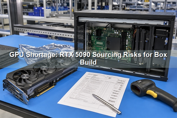
The September 7, 2026 GPU shortage snapshot matters to EBest Circuit (Best Technology) when a customer-approved graphics card is part of a Box Build order. RTX 5090 sourcing does not change how we manufacture the surrounding PCBs, but uncertain availability can delay material release, force another mechanical and electrical review, and change the agreed system test. We therefore treat the GPU as a separately approved high-value item within the complete assembly, not as a component that can be substituted by chipset name alone.

GPU shortage and RTX 5090 sourcing for a professional Box Build project

What Does the September 7 RTX 5090 Price Snapshot Show?

The observed listings showed a clear difference between Founders Edition reference prices and orderable add-in-board models. This is a dated channel snapshot rather than a market average. Each row preserves the region, seller, exact item, price and availability observed on September 7, 2026.

Region Channel and exact item Observed price and status Comparison basis
United States NVIDIA Marketplace, GeForce RTX 5090 Founders Edition, MPN NVGFT590 $1,999.00; out of stock Matched NVIDIA’s US launch starting price but was not orderable.
United States Best Buy, Founders Edition, model 900-1G144-2530-000, SKU 6614151 $1,999.99; sold out $0.99 above the US launch reference but was not orderable.
United States Newegg, MSI RTX 5090 32G GAMING TRIO OC, item 14-137-919 $4,699.99; listed in stock An AIB model, so it is not a like-for-like comparison with the Founders Edition.
United Kingdom Scan, MSI RTX 5090 32G GAMING TRIO OC, scan code LN155275 GBP 4,679.99; listed in stock The same MSI model as the US sample, but currency, tax and regional terms differ.

The figures do not support one universal claim about the RTX 5090 market price. Founders Edition and factory-overclocked AIB cards differ in cooler design, dimensions, power settings and commercial terms. For a Box Build order, the useful conclusion is narrower: the project cannot assume that its approved model will be available at the original budget and delivery date.

Illustration comparing availability for the same high-end GPU across two regional channels

Why Does GPU Availability Matter to a Box Build Manufacturer?

A discrete high-end GPU enters the Box Build during system integration, but its availability affects decisions made before assembly starts. We need the approved manufacturer part number and the selected material-supply model before confirming the integration schedule.

  • Material release: The assembly schedule must reflect when the approved GPU will actually arrive and pass the agreed receiving checks.
  • Mechanical fit: Card length, height, slot width and power-connector position affect the enclosure, brackets and cable clearance.
  • Power and thermal inputs: The selected card affects the PSU, connector arrangement, airflow plan and system-level thermal check.
  • Test preparation: The operating system, driver, display outputs and acceptance load must match the approved configuration.
  • Change control: A different RTX 5090 model is an engineering change when it alters any of these inputs, even if the GPU family name is unchanged.

This is the direct connection between the news and our manufacturing work. The channel price itself is outside our control; the material handoff, integration inputs and agreed production tests are the parts that must be controlled within the Box Build project.

What Must Be Revalidated When the Approved GPU Changes?

Substituting one board partner’s RTX 5090 for another can affect more than the purchase price. Before we release a revised configuration, the customer and our engineering team should confirm the items that changed.

Review area Required input Manufacturing consequence
Enclosure fit Card dimensions, slot width, bracket and connector location Confirms clearance, retention and cable routing.
Electrical interface Power connector, PSU rating and motherboard compatibility Confirms the released cable and power configuration.
Thermal design Cooling layout, airflow direction and operating load Determines whether the enclosure and fan plan need another review.
Software setup Approved driver, firmware and operating-system image Keeps the functional-test configuration consistent.
Acceptance test Boot, output, load and temperature criteria agreed for the system Defines what our production test can verify after integration.

These checks do not require BestPCBs to forecast GPU prices or recommend a retail channel. They ensure that a customer-approved change does not create a preventable assembly or test problem.

How Should GPU Availability Be Reflected in the Production Schedule?

The GPU delivery date should not automatically hold every part of the project, but the manufacturing plan must separate work that has stable inputs from work that depends on the final card. This prevents an uncertain delivery promise from becoming an unexamined Box Build completion date.

  • PCB and PCBA production: These stages can proceed when the electrical interfaces, board revisions and approved BOM are frozen independently of the GPU model.
  • Enclosure and cable preparation: Production can proceed only after the selected card’s dimensions, bracket and power-connector position are confirmed.
  • Final integration: The schedule should begin from the confirmed receipt of the approved GPU and completion of the agreed incoming checks.
  • System testing: Test time should follow installation and use the approved driver, operating-system image and acceptance criteria.

When these dependencies are visible, we can plan the surrounding manufacturing work without claiming that an unreceived GPU is available. If the approved model changes, only the affected steps need to be reviewed and rescheduled.

Who Should Supply the GPU for a Box Build Project?

Box Build procurement can use full-turnkey, partial-turnkey or consignment arrangements. For a volatile and high-value item, the appropriate model depends on who has the approved source, who accepts the quoted price and who owns the supplier warranty.

Supply model Customer decision Our manufacturing role
Customer supplied material Purchase the approved GPU and retain the original supplier and warranty relationship. Receive, record, store, kit, install and test it according to the agreed project requirements.
Customer-nominated source Approve the exact seller, part number, price and commercial terms before purchase. Purchase only after approval, then process the item through the agreed receiving and assembly flow.
Assembler sourcing Approve the quoted item, validity period and any permitted alternative. Source against the approved BOM when availability and terms can be confirmed for that order.

EBest Circuit (Best Technology) does not claim to manufacture GPUs or hold RTX 5090 inventory. Availability and warranty must be confirmed for the exact seller and order date. Our responsibility is limited to the sourcing scope accepted in the order and the manufacturing work performed on the complete assembly.

Customer supplied material control from receipt through Box Build testing

What Information Should Accompany a Customer-Supplied GPU?

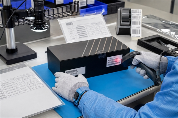
Customer supplied material needs a clear manufacturing handoff. For component traceability within the Box Build record, the customer should identify the approved manufacturer part number, quantity and any serial-number mapping required for its service process.

Incoming inspection and component traceability for a high-value GPU
  • Approved manufacturer part number and permitted revision or alternative.
  • Expected quantity and any project-specific serial-number requirement.
  • Packaging condition or handling requirement that must be checked at receipt.
  • Instructions for discrepancies, transit damage or a unit that fails the agreed incoming or system test.
  • The party responsible for supplier contact, return authorization and replacement material.

Our receiving record can document what entered the manufacturing flow and which unit was installed when serial mapping is required. It does not certify the internal authenticity of a GPU or replace the original supplier’s warranty.

What Can EBest Circuit Support Around the GPU?

At EBest Circuit (Best Technology), our relevant work is the electronics and assembly around the approved GPU. Our PCB assembly service supports SMT, through-hole and mixed assembly for control, power and interface boards. We can manufacture the project’s FR4 control and I/O PCBs, and high-Tg PCB construction is available when the board design and operating conditions justify it.

Depending on the approved project scope, we can also support component sourcing, incoming material checks, cable and enclosure integration, final assembly and agreed functional testing. SPI, AOI and X-ray apply where appropriate to the PCBA being manufactured; they should not be presented as proof of GPU authenticity. The exact Box Build test must be defined from the customer’s system requirements.

What Should Be Confirmed Before Production Release?

Before production release, the project should identify the exact GPU, supply model, expected delivery date, permitted alternatives, enclosure and power inputs, required serial records, warranty contact and system acceptance test. Once those items are agreed, we can plan the surrounding PCB, PCBA and Box Build work without treating an uncertain retail listing as confirmed production material.

For a project affected by the current GPU shortage, send the approved system BOM and assembly requirements to sales@bestpcbs.com. We will review the manufacturing scope and identify which GPU-related inputs must be supplied or approved before the order is released.

You may also like

Vapor Phase Soldering: Process, Profiles & Practical Limits

September 4th, 2026

Vapor phase soldering heats a PCB assembly by condensing hot vapor on its cooler surfaces. The released heat melts the solder alloy in the paste and forms the joints. Also known as condensation soldering or vapor phase reflow, this method can help when large, slow-heating parts share a board with small, temperature-sensitive components.

Its main appeal is controlled heat transfer across that mixed assembly. The fluid limits the heating temperature; it does not guarantee a good solder joint. Fluid selection, the measured board profile and inspection results still determine whether the process suits the PCB.

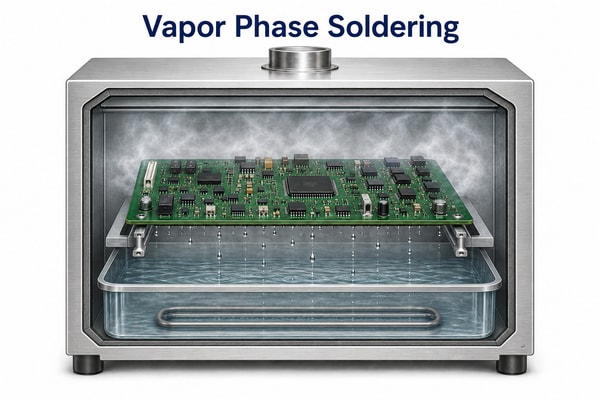
Vapor phase soldering, illustrative laboratory reflow equipment and a populated PCB carrier with the article title

How Does Vapor Phase Soldering Work?

When vapor condenses on the PCB, it releases latent heat directly to the board and components. The vapor comes from a purpose-made heat-transfer fluid, not water. That fluid carries heat; the solder paste supplies the metal that joins each component termination to its pad.

In a conventional saturated-vapor machine, heaters boil the fluid beneath a controlled vapor zone. A carrier holds the assembly in that zone while condensate forms on its surfaces and drains back into the reservoir. Some machines instead meter fluid into a process chamber, so the loading and vapor-delivery sequence depends on the equipment.

Condensation heating falls as the board approaches the vapor temperature. At a given pressure, the fluid’s boiling point sets the temperature ceiling for this heating method. A component rated below that temperature can still be damaged, while a heavy copper area may take longer to reach soldering temperature.

Vapor phase soldering, conceptual chamber cutaway with a populated PCB on a carrier above heat-transfer fluid and condensate returning to the reservoir

What Are the Steps in Vapor Phase Soldering?

After solder paste printing and component placement, the board moves through loading, preheating, reflow and cooling. Vacuum may be added during the molten-solder stage when the process calls for it.

  • Prepare the board before heating. Verify the board revision, paste, component orientation and moisture-handling requirements. Inspect the deposits and placement: reflow cannot repair missing paste or a wrongly fitted part.
  • Load the board on a stable carrier. Allow for its outline, weight and underside components. Supports must hold the assembly through heating and cooling without pressing on parts.
  • Preheat at the required rate. Adjust preheat or vapor delivery to suit the paste and component limits. The measured ramp and soak should allow flux activation and volatile release without excessive thermal stress.
  • Bring the critical joints through reflow. Hold them within the required temperature and time limits. Check both the slowest-heating joints and the most heat-sensitive components.
  • Apply vacuum only when the process includes it. Coordinate pressure and timing with the molten-solder interval. Save the pressure cycle alongside the temperature trace so the result can be repeated.
  • Cool before unloading and inspection. Recover the working fluid and keep the board supported as the joints solidify. Inspect accessible and hidden joints using the specified methods, then complete the electrical tests.

Vapor phase reflow does not require vacuum. A non-vacuum machine can produce acceptable joints when the profile, materials and assembly meet the product’s requirements.

What Fluid Is Used in Vapor Phase Soldering?

Common vapor phase soldering fluids are perfluoropolyethers, or PFPEs. The selected grade sets the nominal vapor temperature at the operating pressure. Grades with similar names or boiling points are not necessarily interchangeable.

Galden LS/HS grades, for example, are designed for vapor phase soldering; general-purpose HT grades have different distillation-range and vapor-temperature controls. Choose a soldering fluid that matches the machine specification, solder paste and component limits.

A 230°C fluid will not become a 245°C heat source because the board stays in longer. In saturated vapor at the specified pressure, extra dwell gives colder joints more time to approach the vapor temperature. If the paste needs a peak the fluid cannot provide, change the fluid, paste or process.

Include fluid recovery, maintenance and consumption in the operating-cost estimate. Follow the current technical and safety data for machine compatibility, hot-fluid handling and disposal; chemical inertness does not remove those precautions.

How Do You Measure a Vapor Phase Soldering Profile?

Measure temperatures on the assembly, rather than judging the profile from the vapor reading alone. A vapor phase soldering temperature profile needs to show how the critical joints and components heat, dwell and cool.

Place thermocouples at a large thermal pad or copper-rich area, a small fast-heating location and a temperature-sensitive component. Identify whether each sensor measures a joint or a package body—their limits may differ. Use the intended carrier and a representative production load.

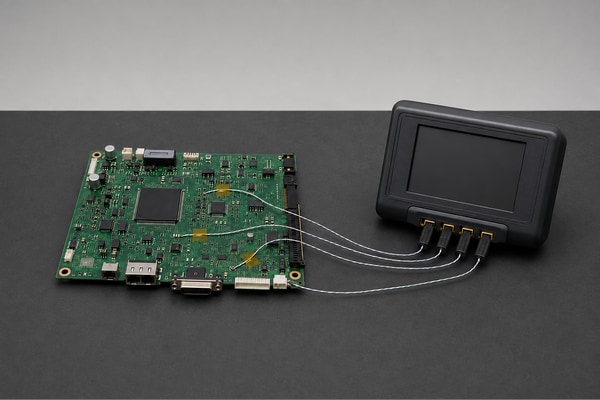
Vapor phase soldering, illustrative PCB with thermocouple leads connected to a logger with a blank display
  • Heating rate and soak: look for uneven heating. If small parts heat much faster than a large pad, adjust preheat or vapor delivery and measure again. Keep the ramp and dwell within the paste and component limits.
  • Peak temperature: both hot and cold locations must pass. The coldest critical joint must reach the paste’s process window while the hottest monitored component stays within its limit.
  • Time above liquidus: measure each critical joint. Too little time above the alloy’s liquidus temperature can leave incomplete wetting. Extending that interval also affects flux behavior and intermetallic growth, so use the paste’s specified window.
  • Cooling: keep recording until the joints solidify. Check the specified cooling limits and keep the assembly supported. Stopping the trace at peak temperature leaves this part of the profile unverified.

There is no universal temperature recipe for VPS. Indium Corporation gives a preferred peak of 230–240°C for the SAC pastes in its vapor-phase application note, and 30–90 seconds above liquidus for the Pb-free no-clean pastes it describes. Those ranges apply to the materials discussed. Set your trial from the current paste data sheet and the most restrictive component limits.

What Causes Common Vapor Phase Soldering Defects?

Trace defects through paste printing, placement and the measured profile before changing the heat settings. Note which parts fail and when the problem first appeared. A lifted resistor and a solder bridge may need very different corrections.

  • Tombstoning: compare the two ends of the lifted part. Unequal wetting forces can pull a small resistor or capacitor upright. Check paste volume, placement and whether the copper connections make one pad heat sooner. If printing and placement are balanced, try a gentler ramp within the paste’s limits and recount defects at those locations.
  • Component shift: find out when the part moves. Check its position and paste alignment before reflow. Movement that begins only with vacuum calls for a pressure-trace review. Trial a less abrupt evacuation cycle without losing the required soldering conditions, then inspect for beads and bridges as well as alignment.
  • Excessive voiding: check the joint before increasing vacuum. Poor wetting or insufficient solder can leave unfilled areas as well as trapped gas. Compare X-ray patterns, deposit volume, paste condition and the joint profile. Once those are stable, assess a controlled vacuum trial using the same imaging method and acceptance limit.
  • Solder balls or spatter: review paste handling and the heating ramp. Rapid heating can contribute to volatile release and spatter; poor coalescence can leave separate particles. Check deposit shape and trial the recommended preheat conditions. If the defect begins with vacuum, review the evacuation rate too.
  • Incomplete wetting: separate a heat problem from a surface problem. Verify joint peak temperature and time above liquidus. If both meet the material requirements, investigate pad and termination solderability, contamination, paste condition and flux performance before adding heat.
  • Bridging: correct excess paste or placement offset first. Look for paste between adjacent pads and misaligned parts. If both printing and placement are sound, investigate slump or movement during heating and vacuum. Change one suspected cause at a time so the next build shows whether it helped.

Compare defect counts across similar batches, not just one clean board. Keep an unchanged reference build where practical and inspect the same locations after each adjustment. Repeat at representative production loads before treating the correction as stable.

How Does Vacuum Vapor Phase Soldering Reduce Voids?

Vacuum lowers the pressure around molten solder, helping trapped gas expand and escape before the joint solidifies. Paste control, pad design and wetting remain important because vacuum cannot correct every cause of an unfilled joint.

The pressure level, evacuation rate, dwell and solder temperature work together. An abrupt pressure change can disturb the solder or shift components. More aggressive vacuum is not automatically a better process.

Where practical, compare the existing process with VPS both with and without vacuum. Keep the board, paste, stencil and inspection method unchanged. Measure void area and location, then inspect for displaced parts, beads, bridges and insufficient solder.

Accept a low-void result only against a defined measurement method and limit. Agree which joint area is measured and how the percentage is calculated. Use suitable X-ray inspection of hidden solder joints to assess the trial boards; neither a machine’s advertised figure nor an X-ray result alone establishes lifetime reliability.

Vapor Phase vs Convection Reflow: What Is the Difference?

Vapor phase uses condensation to deliver heat; convection reflow uses circulating hot gas. Both reflow solder, so VPS is a type of reflow soldering rather than an alternative to reflow itself.

Process factor Vapor phase Convection reflow
Heat delivery Vapor condenses on cooler surfaces and releases latent heat. Circulating heated air or nitrogen transfers heat to the assembly.
Profile control Fluid grade, preheat, vapor delivery, exposure and pressure depend on the machine. Zone temperatures, gas flow and transport speed shape the profile.
Mixed thermal mass Strong condensation heat transfer can help heat large and small features within one process window. Zone and transport settings must bring cold joints into range without exceeding hot-part limits.
Process atmosphere The working-fluid vapor provides an inert environment in the soldering zone. Air and nitrogen configurations are available.
Void reduction A vacuum option can remove gas while solder is molten. Selected systems also include vacuum; it is not exclusive to vapor phase.

Compare joint quality, temperature spread and accepted boards per hour on the same assembly. Keep the board revision, paste, placement quality and inspection criteria consistent. Batch and inline handling are separate choices; commercial VPS equipment is available in both forms.

When Should You Use Vapor Phase Soldering?

Consider VPS when getting a cold joint hot enough pushes another component too close to its temperature limit. That conflict in the measured profile gives a clearer reason to try the process than board size, package name or order volume alone.

  • Large boards with uneven heating. Power planes, thick copper and large connectors heat differently from small chip components. A useful VPS trial should show a smaller temperature spread at the critical locations while all monitored parts stay within their limits.
  • BGA packages with difficult thermal profiles. Vapor phase soldering for BGA assemblies can help heat a large package and its underlying joints. Pad design, paste deposits, warpage and moisture still affect the result, so combine board profiling with hidden-joint inspection.
  • Power devices where voids affect the thermal path. A vacuum-capable process may help large soldered thermal pads. Define the X-ray method and joint-specific limit before the trial; void location and the largest void can matter alongside total void area.

Keep convection if it already delivers acceptable joints, a repeatable profile and the required output at a suitable cost. Rule out printing, placement and material problems before changing the heating method. If voiding is the only remaining issue, compare vacuum options in both types of equipment.

A difficult low-volume board may justify VPS for thermal control alone. In repeat production, weigh any quality improvement against loading, cooling, inspection and fluid costs. The trial needs to show an improvement worth the added cost or cycle time.

What Are the Disadvantages of Vapor Phase Soldering?

The main drawbacks are fluid costs, equipment costs, setup work and cycle time that varies with the load. Efficient heat transfer is useful only when its rate stays within the assembly’s limits.

  • The board can heat too quickly. Even a fluid with the right boiling point needs controlled preheating and exposure. Test the ramp and dwell at the intended load, where fast-heating parts may approach their limits sooner.
  • The fluid temperature may not suit every material. It may be too low for the paste or too high for a component. Resolve conflicting limits before production; a longer dwell cannot fix that mismatch.
  • Fluid recovery adds running costs. The initial charge, carry-out losses, filtration and maintenance all count. Compare consumption for the proposed load and handling method as well as the fluid purchase price.
  • Cooling and handling can limit output. Include loading, preheat, vacuum, cooling and unloading in the cycle estimate. A short reflow step alone does not tell you how many boards the machine can deliver.

Normal moisture-control requirements still apply. Staying below the fluid’s boiling point does not prevent damage from trapped moisture, excessive exposure or an unsuitable material.

How Do You Verify Vapor Phase Soldering Quality?

A good temperature trace must be backed by acceptable joints and the required test results. Set the acceptance limits before the trial, then keep the following information together so the approved build can be repeated.

  • Start with a defined board and material set. Keep the PCB and assembly revisions, construction, component list, paste product and lot, solder alloy and fluid grade together with their temperature, moisture and joint-acceptance limits. Resolve any conflict before running the trial.
  • Make the loading arrangement repeatable. Note the machine, carrier, supports, board orientation and batch size. Mark sensor positions on a drawing or photograph, including whether each measures a joint or package body. Later profiles can then be compared on the same basis.
  • Save the measured curves and their recipe. For each critical location, retain the ramp, peak, time above liquidus and cooling trace against its limits. A vacuum build also needs pressure, evacuation rate, dwell and timing relative to the molten-solder interval.
  • Keep inspection results tied to the boards inspected. Record the sample count and reference designators, visual or automated optical inspection findings, and required X-ray views. Void results need the measured area, calculation method and limit. Include bridges and shifted parts, even if voiding improves.
  • Test the assemblies and repeat the build. Retain the test procedure, limits and results for each board or batch. Repeat at representative loads using a sample plan matched to product risk. Functional testing alone does not qualify every joint; reliability or destructive tests may also be needed.
  • Define what requires another trial. Name the approver and any unresolved deviations. Changes to paste, fluid, major components, copper construction, loading or recipe may require a new profile or qualification review. Keep the approved settings and supporting results accessible to production.

A trial fails if fixing the cold joint overheats another component. Adjust the available controls, measure both locations again and repeat the affected inspection and tests. The accepted process must suit the whole assembly.

How Do You Choose a Vapor Phase Soldering Machine?

Choose a machine that fits the populated board, can achieve its profile and meets the required output. Compare price only after the quotations include the same necessary functions.

A compact batch vapor phase reflow oven may suit laboratory work or short runs, while an inline system may fit a continuous line. In either case, use the actual board and loading arrangement to judge handling, process control and cycle time.

  • Usable board space and support. Supply panel dimensions, assembly weight, component heights on both sides and support restrictions. The usable carrier area and clearances matter more than the chamber’s outside dimensions.
  • Temperature and vacuum controls. Compare supported fluid grades, heating adjustments, measurement features and pressure-cycle control. For a narrow process window, ask for a trial on a representative board.
  • Fit with the production line. Check loading, cooling, line interfaces, recipe access and process records. Estimate output from the full cycle and planned utilization.
  • Installed and operating costs. Include required options, fluid charge and losses, filtration, utilities, maintenance, labor, qualification and inspection. This makes the machine-price comparison meaningful.

When outsourcing PCB assembly, confirm access to VPS equipment before specifying the process in an order. Ask where the work will be done and which qualification records are included; general SMT capability does not establish VPS availability.

FAQ About Vapor Phase Soldering

Q1: Are vapor phase soldering and vapour phase soldering different?

A1: They are spelling variants. “Vapor” is American English and “vapour” is British English. VPS, vapor phase reflow and condensation soldering commonly refer to the same heating principle. Individual machines may use different vapor-delivery and profile-control methods.

Q2: Does the process need nitrogen?

A2: The basic condensation process does not need a separate nitrogen supply. The working vapor can provide the inert soldering atmosphere. Some machines still use nitrogen for chamber or cooling functions, so confirm the utilities for the model and configuration being considered.

Q3: Can double-sided PCBs use vapor phase reflow?

A3: Yes, with a suitable assembly sequence and carrier. Allow clearance for underside components and consider how they will stay in place during the second heating cycle. Heavy parts may need another sequence or retention method. Trial the populated board on its intended carrier and account for cumulative thermal exposure.

Q4: Does the working fluid remove the need to clean flux residue?

A4: No. Recovering the working fluid does not remove the need to assess flux residue. Cleaning depends on paste chemistry, residue behavior and later operations such as conformal coating. Check the assembled product against its cleanliness and material-compatibility requirements.

Q5: Can vapor phase equipment be used for rework?

A5: Some systems support desoldering and repair with suitable tools and a qualified process. Other components and underside joints also experience the additional thermal cycle. Check their limits and moisture history, then inspect and retest the repaired circuit. Identify the fault before deciding to reflow the board.

Conclusion

Choose vapor phase soldering when trials show a useful improvement in thermal control or joint quality at an acceptable production cost. Match the fluid to the paste and component limits, measure the board profile and evaluate vacuum if voiding remains a problem. A working convection process may already be the better fit.

For a free DFM review with BestPCBS, send your Gerber or ODB++ files, BOM with exact part numbers and allowed alternatives, assembly drawing, quantity, target delivery and inspection requirements to sales@bestpcbs.com.

Include the solder alloy, temperature-sensitive parts and any voiding limit. If VPS is required, ask the team to confirm the process and availability for your project before quotation.

You may also like

When to Use Manual vs Automated PCB Assembly?

September 4th, 2026

Use manual assembly for a few accessible parts, frequent prototype changes or work that needs individual handling. Choose automated PCB assembly for dense layouts, precise component placement and repeat production. Quantity alone is a poor guide: a few fine-pitch boards may need machine placement, while a large production run may still include hand-fitted connectors or cables. Start with the parts on the board, then compare setup costs, inspection needs and the cost of each acceptable finished assembly.

Automated PCB assembly, illustrative PCB fixture and tweezers in front of an enclosed placement machine with the article title

What Is Automated PCB Assembly?

Automated PCB assembly uses programmed equipment to apply solder paste, place components and inspect the assembly. In a typical surface-mount technology (SMT) process, parts are placed onto paste deposits and soldered in a reflow oven. Assembly starts with an already fabricated PCB; manufacturing the bare board is a separate process.

Manual assembly can mean hand placement followed by reflow, hand insertion of through-hole parts, or soldering individual joints with a controlled tool. When comparing quotes, ask which of these operations the supplier means by “manual” and how the finished joints will be checked.

How Does the Automated PCB Assembly Process Work?

An automated SMT line prints solder paste, checks the deposits, places components and reflows the solder before final inspection and testing. The files and materials must be checked first: an incorrect part number or feeder assignment can affect every board in the batch.

Automated PCB assembly, component placement machine with tape feeders photographed on the BestPCBS website
  1. Check the files and component kit. Match the bill of materials (BOM), placement file and assembly drawing to the same revision. Confirm part numbers, orientation, approved substitutions and do-not-populate positions. Resolve any difference between the received parts and the BOM before loading the machine.
  2. Print or dispense solder paste. A stencil printer or dispensing system applies paste to the specified pads. Check the stencil or dispensing program against the board revision and package requirements. The deposits need to match the required locations and amounts before parts are placed.
  3. Inspect the paste deposits. Solder paste inspection (SPI) measures features such as deposit height, area or volume, depending on the system. Review deposits outside the set limits and correct the printing problem before placement. SPI checks paste at this stage; solder-joint inspection follows reflow.
  4. Place the components. The pick-and-place machine takes parts from feeders and uses vision and board reference marks, called fiducials, to position them. Verify feeder assignments and component orientation on the first board. Correct misplaced, missing or wrong parts before continuing the batch.
  5. Reflow the solder. The oven heats and cools the assembly to form the solder joints. Measure the board’s thermal profile and check it against the solder-paste requirements and component temperature limits. Keep the measured profile with the build records instead of assuming another board’s oven settings will work.
  6. Finish and test the assembly. Inspect the reflowed board and complete any remaining through-hole soldering or mechanical fitting in the agreed order. Repeat affected inspections after work that could disturb earlier joints. Record the required electrical and functional test results before releasing the finished boards.

An automated PCB assembly line commonly includes a paste printer, SPI system, pick-and-place machine, reflow oven and optical inspection station. The quoted service may stop short of a finished, tested product. Confirm whether X-ray inspection, firmware programming, functional testing and enclosure assembly are included where needed.

When Should You Choose Manual PCB Assembly?

Manual assembly often suits early design changes, a few easy-to-handle parts and local repair work. It saves machine preparation only if a technician can reach, solder and inspect the parts reliably.

  • The circuit is still changing. A prototype may need different resistor values, added wires or repeated component replacement. Accessible parts can be changed without setting up a new placement program. Record each approved modification so the next revision reproduces the working circuit.
  • There are only a few accessible parts. Hand placement may take less time than preparing feeders and a machine program for a simple board. Compare the actual placement and inspection labor with the setup charge. A small batch with difficult packages may still favor automation.
  • A few parts need individual handling. Loose wires, unusual connectors or mechanically secured parts may be easier to fit at a manual station. Check soldering-tool access, board support and component temperature limits. For repeat orders, ask whether dedicated feeding or fitting tools would reduce the handwork.
  • A board needs local repair. A technician can investigate a specific fault, replace the affected component and retest that circuit. Define the repair method and checks before starting, and record what was changed. Repeated repairs at the same location also call for a review of the original assembly process.

Manual work still needs electrostatic discharge (ESD) protection, part-number checks, controlled soldering and inspection. If joints sit beneath the package, confirm how solder will be applied and how those hidden joints will be assessed before choosing hand placement.

When Does Automated PCB Assembly Make More Sense?

Automation makes more sense when a board has dense placement, difficult packages or enough repeat work to reuse the setup. Small batches can qualify too: package size and access may matter more than the number of boards.

  • Small components or dense layouts make hand placement difficult. Tight spacing leaves less room for tools and increases placement demands. For quad flat no-lead (QFN) packages, check the PCB lands, paste volume and reflow profile together. Accurate machine placement cannot correct an unsuitable paste deposit.
  • The same design will be built again. Placement programs and inspection settings can be reused after checking for revision changes. Give the assembler the first-order quantity and likely repeat quantities, then ask which setup charges recur. Keep forecasts separate from committed orders.
  • Hand placement is slowing the batch. Measure placement time alongside inspection and testing time. Automation helps throughput when placement is the limiting operation. If functional testing takes longer or components are missing, a faster placement machine will not remove that delay.
  • The work must repeat across shifts. Verified machine settings reduce dependence on each operator’s placement technique. Check the first assembly before releasing the batch: a wrong feeder assignment or program can repeat the same defect on every board.

For high-mix, low-volume production, ask how long component preparation, program verification and line changeover take for each design. These tasks can outweigh the placement time on a short run. For larger runs, check that feeder replenishment, secondary soldering and testing can keep pace with the placement machine.

How Do Manual and Automated PCB Assembly Compare?

Compare both routes for the same board revision, quantity and inspection requirements. Otherwise, a lower unit price may simply cover less work.

Build factor Manual route Automated route
Design changes Accessible changes can be made with limited setup; document every modification. Changed data and programs need verification; stable revisions make reuse easier.
Placement workload Useful for a few accessible parts; labor grows with placements and handling difficulty. Useful for dense or repeated placement; feasibility depends on packages, feeders and tooling.
Special operations Flexible for cables, special fitting and controlled local rework. May require dedicated tooling; suitable repeat operations can justify it.
Cost structure Often less programming effort, with more direct labor per assembly. Setup and tooling are spread across the batch; changeovers still consume resources.
Quality control Needs documented workmanship, inspection and the agreed electrical tests. Needs validated inputs, process monitoring and the same agreed acceptance criteria.

When Is a Hybrid PCB Assembly Process the Best Fit?

A hybrid process suits boards whose SMT components can run through the line together, while a few parts need separate fitting or soldering. The assembler assigns a method to each operation, so the same board can use both automated and manual work.

Consider a hypothetical industrial controller with surface-mount resistors and ICs, a through-hole terminal block and a wired connection to an enclosure. The SMT components can be printed, placed and reflowed together. The terminal block can then use a qualified through-hole soldering operation, while wire attachment and mechanical fitting may remain manual.

Automated PCB assembly, populated PCB with surface-mount ICs, capacitors and several board connectors, photographed on the BestPCBS website

Mixed-technology PCB assembly means the board uses both SMT and through-hole components. It does not necessarily mean manual plus automated work; through-hole insertion and soldering can also be automated.

Ask for the operation sequence before approving a hybrid build. It should show when special parts are fitted, which parts can pass through reflow or cleaning, and when inspection takes place. Later fitting, soldering or board separation may affect joints that passed an earlier check.

When Does Automated PCB Assembly Become Cost-Effective?

Automation becomes cheaper when the savings per board cover its extra setup and tooling costs. Both methods must first meet the board’s assembly and test requirements. There is no universal break-even quantity; use the charges quoted for your order, rather than a machine supplier’s production-speed claim.

A simple batch model is:

Total assembly cost = setup cost + quantity × variable assembly cost per board

The variable cost should cover the same placement, soldering, inspection and test scope. Keep bare boards and components separate if their costs are identical. If a route changes material losses, scrap or rework, include those differences before making a decision.

To compare cost per board, divide each route’s total batch cost by the number of acceptable assemblies delivered. Include setup, secondary soldering and testing before comparing the result with a quoted placement charge.

Illustrative calculation, not a supplier quote: assume the manual route costs $120 to set up plus $18 per board, while the automated route costs $600 to set up plus $6 per board. Both are assumed feasible, with equal test coverage and no difference in material losses.

Break-even quantity = ($600 − $120) ÷ ($18 − $6) = 40 boards

  • At 20 boards: manual assembly totals $480 and automation totals $720. Manual assembly is $240 lower under these assumptions.
  • At 40 boards: each route totals $840. This is the equality point for this example, not an industry threshold.
  • At 100 boards: manual assembly totals $1,920 and automation totals $1,200. Automation is $720 lower, provided the assumptions remain valid.

This example assumes automation has both the higher setup cost and the lower variable cost. With those setup charges, equal or higher automated per-board costs would give no positive break-even quantity. Recalculate if repeat-order setup charges, programming changes, scrap or rework alter either quote.

Check lead time separately from cost. The delivery estimate should include material availability, engineering preparation, the production slot and testing time—not just time on the placement machine.

How Is Quality Controlled in Automated PCB Assembly?

Quality control starts with the correct parts and settings, then checks paste deposits, placement, solder joints and required electrical functions. When the same defect recurs, investigate its cause. Replacing a faulty joint on each board will not correct unstable printing or a wrong machine setting.

Automated PCB assembly, enclosed SINIC-TEK optical inspection station and monitor photographed on the BestPCBS website
  • Check paste before placing parts. SPI flags deposits that are too small, too large or misplaced relative to the programmed limits. Look for repeated failures at the same pads or board locations, then correct the printing setup before more boards enter placement.
  • Inspect visible parts and joints. Automated optical inspection (AOI) checks programmed features such as component position, polarity and visible joints. Review flagged conditions against the acceptance criteria and recheck the program after a design or component change. Electrical testing is still needed to verify the specified circuit behavior.
  • Assess joints hidden beneath packages. Optical inspection cannot directly see joints under ball grid array (BGA) packages. Agree whether the board needs X-ray inspection, what features will be assessed and whether every board or a sample will be checked. An image of a joint does not establish the product’s long-term reliability.
  • Measure the required electrical characteristics. In-circuit testing (ICT) or flying-probe testing can check specified nets, components or measurements where test access allows. Ask which checks the quoted test covers and what limits apply. Compare fixture costs and test time when choosing between methods.
  • Test the required operating functions. Provide the firmware, power conditions, loads, interfaces and pass/fail limits for functional testing. Specify which results must be recorded for each unit. A test at one operating point covers that condition, not every function or environmental limit.
  • Keep the build and repair records. Record the board revision, agreed lot or serial identifiers, repairs and subsequent checks. Specify any additional traceability requirements before ordering so the assembler can include the records, handling and time in the quote.

Select inspection and testing for the board’s packages, functions and failure risks. List each required check, when it occurs and what constitutes a pass. If two suppliers quote different test coverage, resolve that difference before comparing unit prices.

What Should You Ask an Automated PCB Assembly Manufacturer?

Ask how the supplier will assemble your board, approve the first unit and control later batches. The answers should refer to your files and parts, rather than repeat a general equipment list.

  1. Identify parts that need special work. Ask which parts need manual fitting, separate soldering or dedicated tooling, and why. Resolve concerns about package handling, temperature limits or tool access before the batch starts.
  2. Agree how the first assembly will be approved. Specify the part-number, polarity, workmanship and test checks required before the remaining batch proceeds. Name who can resolve a discrepancy and where the approval will be recorded.
  3. Check revision control for repeat orders. Ask how BOM changes and approved substitutes reach the placement and test programs. Put the released revision on each repeat order so an old sample or program cannot silently become the build instruction.
  4. Confirm what the price includes. Separate setup, tooling, assembly, testing and materials where applicable. Ask who owns the tooling, which setup costs recur and how many extra customer-supplied parts are needed for setup or handling losses. These details can change the cost of both the first batch and repeat orders.

What Files Do You Need for an Accurate PCBA Quote?

Send matching PCB files, placement data and a BOM, along with quantities, delivery dates and test requirements. Missing or conflicting revisions can leave the assembler pricing a different board from the one you intend to order.

  • PCB files and component positions. Send Gerber and drill files or another format the supplier accepts, plus component reference designators, coordinates, rotation and board side. Include an assembly drawing and mark do-not-populate positions. Check that all files carry the same revision.
  • Part numbers and sourcing instructions. List manufacturer part numbers, quantities per board, packages and acceptable alternatives in the BOM. Identify customer-supplied parts and whether they arrive on reels, trays or cut tape. For component sourcing, state the required traceability and who must approve substitutions.
  • Quantities and delivery dates. Give the first-order quantity, likely repeat quantities and required delivery date. Mark forecasts as forecasts. Ask the supplier to confirm timing after checking component availability and production capacity.
  • Test and finishing requirements. Include workmanship criteria, firmware files, test procedures, operating limits and required reports. List any cleaning, coating, labeling, wiring or enclosure work. Identify who supplies fixtures and test software so these costs are included.

If the design is unfinished, mark the open items and request an estimate with stated assumptions. Obtain an updated quote once the production files are released.

How Can BestPCBS Support Automated PCB Assembly Projects?

BestPCBS offers SMT, through-hole and mixed-technology PCB assembly, with prototype, component sourcing and box build services. Send the actual BOM and assembly files so the quotation can identify automated work, manual operations and any special tooling your board needs.

  • Prototype and repeat-production assembly. A prototype build can reveal fitting or assembly issues before you order repeat quantities. Share expected production volumes and unresolved design changes with the first-build files. Record approved corrections in the production revision.
  • SMT and through-hole assembly on the same board. BestPCBS can quote both types of work together. Include connectors, wires and mechanical clearance details so the quote covers the parts that need separate fitting or soldering, as well as machine-placed components.
  • PCB fabrication, sourcing and assembly. Turnkey service brings these purchases into one coordinated order. Specify approved component alternatives and substitution approval requirements so availability changes do not lead to unapproved parts in the build.
  • Wiring and enclosure assembly. Box build assembly adds work beyond the populated PCB. Send enclosure drawings, wire or harness details and final test requirements so the quote defines what you will receive as a finished unit.

A free design-for-manufacturing (DFM) review is available with your files. Flag difficult packages, access restrictions or planned quantity changes that may affect the assembly method.

Common Questions About Automated PCB Assembly

Q1: Can automated PCB assembly use cut tape instead of full reels?

A1: Often yes, if the strips meet the assembler’s feeder requirements. Before shipping parts, confirm minimum strip length, any empty tape needed for loading, component orientation and extra quantities for setup or handling losses.

Q2: Can both sides of a PCB be assembled automatically?

A2: Yes, after checking the process for both sides. Submit placement data for each side. The assembler needs to determine the build order, check repeated heat exposure and confirm how parts and the board will be supported during the second-side operation.

Q3: Should heat-sensitive components always be soldered by hand?

A3: No. Check the component’s temperature limits first. Hand soldering can also overheat a part. Compare the manufacturer’s limits with the proposed oven or local soldering process; some parts may need fitting after reflow.

Q4: Can production begin while some supplied components are missing?

A4: Sometimes, but agree how the missing parts will be added first. Later fitting may require extra handling, another soldering operation and repeat inspection. Check tool access, added costs and the revised schedule before approving a partial build.

Q5: How should I compare assembly yield figures?

A5: Check what passed, which tests were used and whether repairs are included. First-pass yield generally counts units that pass the defined process without rework. Final yield may include repaired units. Compare figures from equivalent builds and test coverage.

Q6: What should transfer from a prototype into a repeat production build?

A6: Transfer the released files and the instructions needed to reproduce the build. Include approved modifications, substitutions, process settings and test requirements. A working sample cannot replace the records needed to assemble and check the next batch.

Q7: Is automatic PCB assembly the same as SMT assembly?

A7: No. Automation describes how work is done; SMT describes how components are mounted. SMT commonly uses machine printing and placement but may still include manual work. Through-hole insertion and soldering can also be automated. Ask which operations the quoted service automates.

Conclusion

Use handwork where access and frequent changes make it practical. Use automated PCB assembly where the components or repeat workload justify machine setup. A mixed process is often appropriate; compare the total cost and test coverage for the finished board.

Email your BOM, PCB files, placement data, quantities and required delivery date to sales@bestpcbs.com for an assembly quotation. Include approved alternatives, sourcing and traceability requirements, and the tests your product needs.

You may also like

Soldering Temperature Guide for PCB and Electronics

September 3rd, 2026

Choosing the right soldering temperature is not as simple as setting an iron to one number and using it for every joint. For most electronics work, a soldering iron tip is commonly set somewhere around 315–350°C (599–662°F) for leaded solder and 340–370°C (644–698°F) for common lead-free solder. These are practical starting ranges rather than universal limits.

The correct setting also depends on solder alloy, PCB copper area, tip geometry, component size, flux activity, and how quickly the soldering station can replace lost heat. A small SMD pad may solder cleanly near the lower end of the range, while a connector tied to a large ground plane may need a larger tip, preheating, or a modest temperature increase.

Soldering temperature guide for PCB and electronics showing a temperature-controlled soldering station and PCB hand soldering

What Is the Best Soldering Temperature for Electronics?

For general electronics soldering, about 320–350°C is a useful starting range for leaded solder, while 340–370°C is more typical for lead-free solder.

The temperature should be high enough to heat the pad, component lead, and solder quickly, but not so high that flux burns away before the joint forms.

A practical starting point is:

  • Fine electronic wiring or small pads: 300–330°C
  • General PCB work with leaded solder: 320–350°C
  • General PCB work with lead-free solder: 340–370°C
  • Large connectors or high-copper areas: often near the upper end of the range, preferably with a larger tip or PCB preheating

The best soldering temperature is therefore the lowest setting that can bring the entire joint to soldering temperature within a short, controlled contact time.

If the iron must remain on the joint for a long time, simply using a lower temperature is not necessarily gentler. Extended heating can transfer more total energy into the PCB and component than a slightly hotter tip used briefly.

Soldering Temperature Chart for PCB and Electronics

The following soldering temperature chart provides practical starting values for common electronics work.

Application Solder / Process Melting or Liquidus Temperature Practical Starting Setting
General PCB hand soldering Sn63/Pb37 183°C 320–350°C
General PCB hand soldering Sn60/Pb40 About 183–190°C 320–350°C
Lead-free PCB soldering SAC305 About 217–220°C 340–370°C
Fine SMD hand soldering Leaded About 183°C 300–330°C
Fine SMD hand soldering Lead-free About 217–220°C 320–350°C
Large PCB connector Leaded About 183–190°C 340–370°C*
Large PCB connector Lead-free About 217–220°C 350–380°C*
Leaded hot-air rework Process dependent — About 300–350°C display setting*
Lead-free hot-air rework Process dependent — About 320–380°C display setting*
Leaded desoldering SnPb About 183–190°C 330–370°C*
Lead-free desoldering SAC-type alloy About 217–220°C 350–390°C*

*These values depend strongly on thermal mass, equipment calibration, nozzle or tip size, airflow, and preheating.

The table should be treated as a setup reference rather than a process specification. The actual solder joint temperature is different from the temperature shown on the soldering station.

Soldering temperature chart for leaded, lead-free, SMD, hot-air rework and desoldering

Why Is Soldering Iron Temperature Higher Than the Solder Melting Point?

A soldering iron is normally set far above the solder’s melting point because heat must travel from the heater through the tip and into the complete joint.

For example, Sn63/Pb37 solder melts at 183°C, but setting an iron to 183°C would usually provide very little thermal margin. As soon as the tip touches a copper pad, heat begins flowing into:

  • the copper track,
  • plated through-hole barrel,
  • component lead,
  • nearby copper planes,
  • and the PCB laminate.

The tip surface can cool substantially during this transfer.

This is why melting temperature and soldering iron temperature are not interchangeable measurements.

Three temperatures are especially easy to confuse:

  • Solder melting temperature: where the alloy changes state.
  • Joint temperature: the temperature actually reached by the pad, lead, and solder.
  • Tip set temperature: the value selected on the soldering station.

A good soldering station compensates quickly when the tip loses heat. A weak station may show 350°C on the display yet struggle on a large ground connection because its heater cannot restore tip temperature fast enough.

Diagram showing why soldering iron tip temperature is higher than solder melting point due to heat flow into the PCB

What Soldering Temperature Should You Use for 60/40 and 63/37 Solder?

For 60/40 and 63/37 tin-lead solder, approximately 320–350°C is a practical hand-soldering starting range for normal PCB work.

The two alloys behave slightly differently.

Sn63/Pb37 is eutectic. It changes from solid to liquid at approximately 183°C without a significant pasty range. This makes the joint relatively easy to form and inspect during hand soldering.

Sn60/Pb40 begins melting at approximately 183°C and becomes fully liquid at around 190°C. It passes through a short plastic or pasty range during cooling.

For both alloys:

  • Small pads can normally use the lower end of the temperature range.
  • Larger terminals may require 340–350°C or slightly more.
  • Large ground planes should first be addressed with a larger tip or preheater rather than excessive temperature.
  • Good flux activity can reduce the time required to achieve complete wetting.

The difference between 60/40 and 63/37 is important, but PCB thermal mass usually has a greater effect on the required iron setting.

What Is the Best Soldering Temperature for Lead-Free Solder?

For common lead-free electronics solder such as SAC305, 340–370°C is a practical starting range for hand soldering.

Lead-free solder typically has a higher melting temperature than traditional SnPb solder. SAC305, for example, has a liquidus temperature around 217–220°C.

However, its higher working temperature does not mean every lead-free joint should automatically be soldered at 380°C or 400°C.

A better approach is to start around 340–350°C and increase only when the joint cannot reach temperature quickly enough.

Lead-free soldering also benefits from:

  • an appropriately sized chisel or bevel tip,
  • a station with good thermal recovery,
  • active flux,
  • clean and well-tinned tip surfaces,
  • and PCB preheating for large thermal masses.

Lead-free processes can oxidize tips faster, so continuously increasing temperature to compensate for a poorly wetted or oxidized tip usually makes the situation worse.

Leaded versus lead-free solder comparison showing melting point and typical soldering iron settings

What Soldering Iron Temperature Should You Use for PCB Work?

For most PCB hand soldering, about 320–350°C for SnPb solder and 340–370°C for lead-free solder provides a useful starting window.

The PCB construction determines how much heat the joint absorbs.

A small pad on a standard two-layer FR-4 board may reach soldering temperature almost immediately. The same component lead connected to a multilayer ground plane can pull heat away from the tip much faster.

Pay particular attention to:

  • Ground and power planes: internal copper spreads heat away from the joint.
  • Heavy copper PCB: thicker copper requires more thermal energy.
  • Large plated through-holes: the barrel conducts heat through the board thickness.
  • Large connectors: metal housings and thick pins act as heat sinks.
  • Thermal vias: arrays of vias can transfer heat into internal or opposite-side copper.
  • Metal-core boards: heat can leave the soldering area rapidly.

When a PCB joint is difficult to solder, using a larger tip with better contact area is often more effective than immediately turning the station hotter.

What Is the Proper SMD Soldering Temperature?

For small SMD hand soldering, about 300–330°C for leaded solder and 320–350°C for lead-free solder is often sufficient when the tip size and flux are appropriate.

Small components have little thermal mass, so they normally do not require the same thermal input as a large connector.

For packages such as 0402, 0603, SOIC, or fine-pitch IC leads, temperature control matters because the pad area is small and repeated heating can weaken the pad-to-laminate bond.

For cleaner SMD work:

  • Use a tip that matches the pad geometry.
  • Apply flux before touching the joint.
  • Keep contact time short.
  • Avoid pressing the tip into the pad.
  • Allow the joint to cool before repeated rework.
  • Use hot air or controlled reflow methods when a package cannot be heated evenly with an iron.

A high temperature is not automatically faster if the tip is too small to transfer heat efficiently.

What Hot Air Soldering Temperature Should You Use for PCB Rework?

For PCB hot-air rework, roughly 300–350°C for leaded assemblies and 320–380°C for lead-free assemblies can be used as initial station settings, but airflow and PCB preheating are equally important.

A hot-air station does not behave like a soldering iron. The displayed temperature is the heater or calibrated air temperature, not necessarily the temperature at the solder joint.

Actual heating depends on:

  • nozzle diameter,
  • airflow,
  • nozzle-to-board distance,
  • component size,
  • board thickness,
  • copper distribution,
  • surrounding components,
  • and whether the PCB is preheated.

A thick multilayer PCB may require a higher displayed air temperature than a thin board, even when the target solder joint temperature is similar.

For large BGAs, QFNs, shielded modules, or high-copper boards, preheating the PCB reduces the temperature difference between the rework area and the rest of the board. This generally allows gentler top-side heating and reduces local thermal stress.

What Desoldering Temperature Should You Use?

For desoldering, about 330–370°C for leaded joints and 350–390°C for lead-free joints is a reasonable starting range, depending on board construction and the removal method.

Old solder can be more difficult to remove because of oxidation, contamination, or poor remaining flux activity.

Before raising the temperature, try:

  • applying fresh flux,
  • adding a small amount of fresh solder,
  • using a wider desoldering tip,
  • improving contact with the joint,
  • preheating large multilayer boards,
  • or using a powered desoldering tool for plated through-holes.

Adding fresh solder may seem counterintuitive, but it introduces active flux and improves heat transfer into an old joint.

Extra care is required on plated through-holes. Excessive temperature combined with prolonged heating can damage pad adhesion or the connection between the hole barrel and internal copper layers.

Hot-air rework and desoldering temperature guide for PCB repair

What Factors Change the Proper Soldering Temperature?

The proper soldering temperature is primarily determined by how efficiently heat moves from the tool into the solder joint.

The most important variables are:

  • Solder alloy: lead-free alloys generally require higher process temperatures than SnPb alloys.
  • Copper area: large pads, planes, and heavy copper remove heat rapidly.
  • Tip geometry: a larger contact surface transfers energy more efficiently.
  • Station power and recovery: higher heater capacity helps maintain tip temperature under load.
  • Flux condition: active flux improves wetting and reduces the time needed to form the joint.
  • Component thermal mass: connectors, switches, shields, and large terminals absorb more heat.
  • PCB thickness: thick multilayer boards usually require more thermal energy.
  • Preheating: raising the overall PCB temperature can reduce the heat demanded from the soldering tool.
  • Contact time: temperature and dwell time must be considered together.

A station temperature therefore cannot be selected from solder alloy alone. Two assemblies using SAC305 may require noticeably different settings because one has small SMD pads while the other has a large connector tied to a power plane.

PCB factors that change soldering temperature including ground planes, heavy copper, thermal vias and connector size

How Can You Tell If the Soldering Temperature Is Too High or Too Low?

The condition of the joint often shows whether the soldering temperature or heat-transfer setup needs adjustment.

Temperature Too Low / Heat Transfer Too Weak Temperature Too High / Heating Too Aggressive
Solder does not wet the pad easily Flux burns or smokes excessively
Joint looks dull, uneven, or incomplete Tip oxidizes quickly
Solder forms a ball instead of spreading PCB surface discolors
Long contact time is required Pads may loosen or lift
Large joints refuse to flow Plastic connectors may deform
Excessive pressure is needed with the iron Components experience unnecessary thermal stress

A cold-looking joint does not always mean the temperature setting is too low. An oxidized tip, insufficient flux, a very small tip, or a large ground plane can produce similar symptoms.

Likewise, a joint that takes too long at 350°C may be improved by switching from a fine conical tip to a larger chisel tip instead of increasing the iron to 400°C.

FAQs About Soldering Temperature

Is 350°C too hot for PCB soldering?

No. Around 350°C is a common working temperature for many PCB soldering operations, particularly lead-free work or joints with moderate thermal mass. For small heat-sensitive pads, a lower setting may be more appropriate.

What is the normal soldering temperature for electronics?

A typical starting range is approximately 320–350°C for leaded solder and 340–370°C for lead-free solder. The final setting should be adjusted according to joint size, tip geometry, copper area, and contact time.

What temperature should I use for 60/40 solder?

For normal PCB hand soldering with Sn60/Pb40, start around 320–350°C. The alloy melts over approximately 183–190°C, but the iron must be hotter to transfer sufficient heat into the complete joint.

What temperature should I use for lead-free solder?

For common lead-free solder such as SAC305, around 340–370°C is a practical hand-soldering range. Large copper areas may require more thermal capacity, but a larger tip or preheater should usually be considered before using substantially higher temperatures.

Why won’t solder melt even when my iron is hot?

The tip may be oxidized, too small, poorly wetted, or unable to transfer enough heat into the joint. Large ground planes and connectors can also draw heat away faster than the soldering station can replace it.

Can too much heat lift PCB pads?

Yes. Excessive temperature, prolonged contact, repeated rework, and mechanical force can weaken pad adhesion and increase the risk of pad lifting. Controlled temperature, suitable tip geometry, flux, and short contact time reduce this risk.

How Can EBest Circuit Support Your PCB Assembly Project?

If you are preparing a PCB or PCBA project and need support with soldering process requirements, assembly manufacturability, or production planning, send your Gerber files, BOM, and assembly requirements to sales@bestpcbs.com. Our engineering team can review the project before production and help identify process conditions that may affect solder-joint quality, component reliability, or assembly yield.

You may also like

Custom Pogo Pin PCB Assembly Services: Design, Prototyping & Production

September 3rd, 2026

A pogo pins PCB assembly can pass a bench continuity check and still disconnect when the enclosure closes or the board bends. The spring-loaded contacts need enough compression to maintain contact, a landing surface that tolerates misalignment, and a board that carries the load without moving out of position. These requirements affect the PCB layout and assembly method before the first prototype is ordered.

EBest Circuit (Best Technology) supports PCB design, fabrication, component sourcing and assembly for prototype and production orders. For a custom pogo-pin carrier, the starting information is the contact part number, mating geometry and electrical load. A sample build can then answer specific questions about fit, contact stability and manufacturability before you commit to production.

Pogo pins PCB, illustrative six-contact green carrier board with a centered title

Which Applications Need a Custom Pogo Pin PCB Assembly?

Pogo-pin carriers suit connections that must separate repeatedly or reach exposed pads without a permanently attached plug. The application determines what to design around:

  • Charging docks: Check the current through both the supply and return contacts, then the force needed to keep the device seated. If charging stops when the device rocks, adding a higher-current pin will not correct the mechanical movement. Guide features and retention belong in the prototype alongside the PCB.
  • Removable modules: Locate the module before its pads touch the plungers. A tapered guide or keyed housing can limit sideways entry; the pins should compress along their intended axis. Mark orientation and power/signal assignments on both drawings so a reversed module cannot silently swap connections.
  • Programming fixtures: Match each probe to an accessible target pad and a defined net. Check tall components, board-location holes and tool access in the same view. For frequently serviced fixtures, a replaceable probe-and-receptacle arrangement may be more practical than soldering every probe directly into the carrier.
  • Functional test fixtures: Separate the force applied by the probe array from the force used to locate the board. Support the unit under test near the loaded area and identify power, return and measurement connections. A carrier PCBA is one part of the fixture; probe plates, wiring, controls and test software must also be accounted for.

How Do You Choose SMT, Soldered Through-Hole or Press-Fit Mounting?

Choose SMT for a surface-soldered contact, through-hole soldering for a solder-tail contact, or a press-fit carrier with a separately specified electrical termination. The useful comparison is how each complete mounting arrangement connects to your circuit and fits your assembly process.

Mounting Option Electrical Connection Selection Trade-off
SMT solder mount The contact base is soldered to a PCB surface pad. Suits a reflow assembly process when the part supports automated pickup. Check pad geometry, seating stability and reflow limits; a tall contact may need a pickup cap or positioning support.
Through-hole solder mount A solder tail passes through the board and is soldered to the specified plated hole or land. Suits a contact supplied with a PCB solder tail. Allow tail clearance and soldering access; match the finished hole and board thickness to the drawing. The hole alone does not prevent tilt.
Press-fit carrier with wire termination The body is retained in a specified hole or housing; a solder cup or attached wire carries the electrical connection. Useful when the contacts must sit in a housing away from the circuit board. Adds wire routing and termination work; control the receiving-hole fit and insertion depth. Do not treat the retaining hole as an electrical joint.

“Press-fit” describes retention unless the manufacturer also specifies an electrical press-fit connection. The Mill-Max 0947, for example, is retained in a non-plated hole or insulator and connects through a solder cup. Its mounting hole does not provide a plated-through-hole electrical path.

A locating peg does not, by itself, identify the soldering method. Some Harwin SMT pogo pins have longer pegs that the manufacturer also permits for throughboard termination. Use the exact part drawing to decide which pad, hole and solder joint to specify.

For a board populated mainly by reflow, first check a compatible SMT part. If the selected contact requires a solder tail, plan the insertion and soldering operation. If the enclosure must hold the contacts separately, evaluate a wired carrier. Current rating, working travel and mating life must still be checked for the selected part; none can be ranked reliably from the mounting label alone.

How Much Compression and Working Travel Does the Assembly Need?

Every pin must remain within its recommended working range at the smallest and largest assembled gaps. Free height describes the unloaded contact; working height describes it under compression. Harwin’s P70-1010045R, for example, has a 5 mm free height and a 4 mm working height. The recommended operating point must not be confused with the absolute end of travel.

Use one mechanical datum for both dimensions: H is the assembled free tip height above that datum, and G is the distance to the mating contact surface. Compression is C = H − G. Include mounting offsets, target thickness and relevant tolerances; do not subtract dimensions taken from different board surfaces.

Worked example, using hypothetical design inputs: H = 5.00 ± 0.10 mm, G = 4.10 ± 0.15 mm, and an allowed compression range of 0.60–1.20 mm. These are illustrative assumptions, not the tolerances or working limits of the Harwin part.

  • Least compression: The shortest installed pin meets the largest gap: 4.90 − 4.25 = 0.65 mm. The margin above the assumed 0.60 mm minimum is only 0.05 mm.
  • Greatest compression: The tallest installed pin meets the smallest gap: 5.10 − 3.95 = 1.15 mm. Only 0.05 mm remains below the assumed 1.20 mm maximum.
  • Board deflection: If loading increases the gap by a further 0.08 mm, minimum compression falls to 0.57 mm. That misses the assumed minimum by 0.03 mm, even though the nominal assembly looked acceptable.

For these inputs, the total worst-case variation in H and G consumes 0.50 mm of the 0.60 mm working window. Only 0.10 mm remains across both ends. Simply moving the nominal gap cannot recover more than that total margin: supporting the board or reducing dimensional variation addresses the missing clearance more directly. Check the assembled gap at both extremes, then verify the proposed change with the actual parts.

Pogo pins PCB, conceptual diagram of free and mated positions with a working-travel arrow

The enclosure should have a mechanical stop before the contact reaches its travel limit. Also add the spring forces at the chosen working position. As a separate illustrative estimate, eight contacts at 0.6 N each oppose closure with 4.8 N before other loads are included. Use the selected part’s force-versus-travel tolerances to size retention and check board bending; magnet pull measured under different gap conditions is not a substitute.

How Should Pogo Pin Mating Pads Be Sized and Finished?

The mating pad must contain the possible contact positions without letting the tip land on solder mask, a via opening or neighboring copper. Size that landing area separately from the solder land used to attach the pin.

For a circular landing area, a conservative geometric starting point is Dpad ≥ Dtip + 2(E + M). Here Dtip is the maximum projected tip diameter, E is the maximum radial position error, and M is the extra edge allowance. Any wipe motion must already be included in E. This checks geometric containment; it does not establish contact pressure, wear life or electrical clearance.

Illustrative pad calculation: Assume a 1.00 mm tip diameter, radial position error of 0.25 mm, and 0.10 mm edge allowance. The calculated minimum diameter is 1.70 mm. At an assumed 2.00 mm pad pitch, only 0.30 mm of copper-to-copper gap remains. Check whether that gap meets the circuit’s clearance needs and whether solder mask can be manufactured as intended before adopting the dimensions.

  • Position error: Include enclosure play, board location, contact placement and target-pad registration. If the drawing gives independent X and Y limits, evaluate their combined radial error; ±0.25 mm on both axes is not a 0.25 mm radial limit.
  • Wear surface: Choose the finish with the expected engagement count and motion in mind. For frequent mating, discuss a wear-rated finish or a separate target contact, and test the proposed pair. A solderability finish alone does not demonstrate acceptable resistance after repeated engagement.
  • Flatness and keepouts: Keep exposed holes, silkscreen and coating away from the swept contact area. When routing requires a via there, define filling, capping and surface flatness with the fabricator rather than accepting an open depression under the tip.

A separate target introduces its own dimensions. Harwin’s S70-332002045R contact pad is a 3.2 mm diameter, 0.2 mm thick gold-finished mating component. It is an example, not the recommended pad for every design. Its installed height, including the solder joint where relevant, changes G in the compression calculation.

How Do You Check Current Capacity, Voltage Drop and Heating?

Start with the allowable voltage loss at the load, then check both the contact rating and the resistance of the complete supply-and-return path. Include the pin, mating interface, solder joints, traces and vias. A catalog rating for one contact does not automatically apply to a closely spaced array inside an enclosure.

Voltage drop is V = I × R; resistive heating is P = I² × R. Suppose each of two mated contacts, one supply and one return, contributes an assumed 0.05 Ω. At 2 A, their combined 0.10 Ω causes 0.20 V of drop and 0.40 W of heating, before PCB and wiring losses. Counting only the supply contact would miss half of this contact contribution.

If the hypothetical product permits only 0.15 V of total connection loss at 2 A, the complete path budget is 0.075 Ω. The two assumed contacts already exceed it. Reducing trace resistance alone cannot fix that selection; investigate a lower-resistance contact arrangement and verify it under the intended compression and load. None of these assumed values establishes a safe temperature or current rating.

  • Load all intended power contacts together: Measure drop and temperature with the enclosure fitted and the contacts at the specified working position. Record ambient temperature and wait for the defined stabilization condition; a brief open-bench reading can miss the final temperature rise.
  • Check parallel paths: Two pins do not necessarily share current equally. Contact variation and unequal routing can concentrate the load in one path. Check the individual branches and decide what the circuit must do if one contact becomes resistive or opens.
  • Assess signal behavior separately: For fast edges, account for the contact geometry, PCB transitions and return path. Check the complete channel with an appropriate model or measurement; a DC continuity or current test does not demonstrate signal integrity.

What Prevents Tilt, Sticking and Damage During Assembly?

Control the fixed barrel’s position during joining, then check installed height and plunger movement after the process. Electrical continuity will not reveal every assembly defect.

  1. Check the exact incoming part: Compare the manufacturer part number, termination, free height and packaging with the BOM and drawing. Hold any substitute for review if its dimensions or force curve differ; matching pitch is not enough.
  2. Establish a repeatable seating position: Use the specified locating feature or fixture and measure from the drawing datum. Check barrel tilt before joining, when correction does not require solder rework. A contact that leans slightly can shift its tip beyond the pad allowance at full height.
  3. Use the part-specific joining process: For SMT, check upright stability, solder distribution and reflow limits. For solder tails, provide access and barrel support. For press-fit retention, support the receiving part and control insertion depth using the approved tooling. Inspect seating and the electrical termination as separate features where necessary.
  4. Measure and exercise the assembled contacts: Check tip heights with suitable metrology or a defined gauge. Compress each plunger within its working range and observe return. Investigate a slow or sticking pin for contamination, damage or process exposure; repeated pressing is not a repair.
  5. Protect the contact array in transit: Keep tray lids and neighboring boards away from the plungers. Check a packed sample for side loading, unintended compression and loose movement so a good assembly is not damaged after inspection.

Compare the first articles with the planned production method. Hand-positioned prototypes do not demonstrate that a tall contact will remain upright through automated placement and reflow. Resolve that difference before using prototype yield to estimate production cost.

How Should Prototypes and Pilot Builds Be Tested?

Test prototypes with the actual mating parts, then use a pilot build to check assembly consistency. Set limits from the device requirements and selected contact specifications before testing; “continuity passed” is too vague to accept a charging or frequently mated interface.

Pogo pins PCB, photorealistic illustrative microscope inspection of a six-contact carrier beside solid target pads
  1. Check fit at the tolerance extremes: Assemble the actual locating and retention hardware. Use measured parts or a controlled fixture to reproduce minimum and maximum gap and lateral offset. Record whether every tip stays on its pad and within working travel, without relying on hand pressure.
  2. Measure the intended resistance: Use four-wire sensing for low-resistance checks, with sense connections close to the two ends of the path being measured. Mark those points on the test drawing; measurements that include different trace lengths are not directly comparable. Record test current, compression and whether the result includes one contact or the complete loop. Use the component’s specified low-level test conditions when checking signal-contact resistance.
  3. Test under operating load: Load the supply and return paths together and measure voltage at the receiving circuit. Log contact-area temperature and ambient conditions until the agreed stabilization point. Compare with the voltage-loss and temperature limits, including worst-case enclosure conditions.
  4. Look for intermittent connections: Reproduce the allowed rocking or movement while monitoring continuity or powered function with time resolution appropriate to the system. A slowly updating handheld meter may miss a brief interruption. Record interruption duration or the resulting reset, communication error or charging fault.
  5. Repeat after the required use cycle: Define engagement count, speed, stroke and relevant contamination or environmental exposure. Compare resistance, loaded performance, tip return and surface wear before and after the test. Keep the mating pad finish and hardware unchanged so a contact-only catalog life claim is not mistaken for a qualified assembly.
  6. Compare the pilot units: Record installed-height spread, tilt, solder or insertion defects, and loaded mating results across the agreed sample. Set production inspection and sampling from the demonstrated process and risk. Identify whether an outlier follows a component lot, fixture position or assembly operation before increasing volume.

If a pogo pins PCB works only when pushed down by hand, check the gap, retention and board deflection first. If failures appear only after cycling, inspect wear and contamination and repeat the same resistance measurement. The test must reproduce the failure condition before it can tell you which change helped.

What Information Is Needed for a Custom Assembly Quote?

Send the board files and the mating requirements together. Otherwise, two suppliers may quote different assemblies even when their board quantities match.

  • PCB files: Supply Gerber or ODB++, drill data, outline, stackup and finish requirements. Include the schematic or net data for electrical review and testing. If design work is still needed, identify the missing files and provide the interface requirements.
  • BOM and sourcing: List manufacturer part numbers, quantities per board and approved alternatives. Attach the contact drawing and installation guidance. State which components you will supply and which EBest should source; replacements that change height or force require renewed mechanical checks.
  • Mating geometry: Provide contact coordinates, datum references, operating gap and tolerances, target-pad dimensions and retention details. Include a STEP model or mating drawing and identify whether the quote includes the carrier only, a mating board, or both.
  • Test requirements: State current per contact, simultaneous loads, voltage-loss limits, engagement requirements and relevant environmental conditions. Name the measurements, limits, sample plan and report expected. For programming, include the image, interface and verification method; identify who supplies the fixture and mating hardware.
  • Order plan: Give prototype quantity, production quantities, required delivery date, traceability and packing needs. Identify the design or sample approvals that must happen before the production order can proceed.

Ask for separate prices for one-time tooling or test setup and recurring assembly. A higher unit quote may include component procurement, a mating board or inspection that another quote omits. Compare the same BOM, quantities, supplied items and acceptance requirements before choosing on price.

Contact availability, PCB fabrication, fixture preparation and sample approval all affect the schedule. Confirm which items are on the critical path and which delivery dates depend on your files or hardware. Send the available documents to sales@bestpcbs.com for a free DFM review and a quotation identifying the remaining inputs.
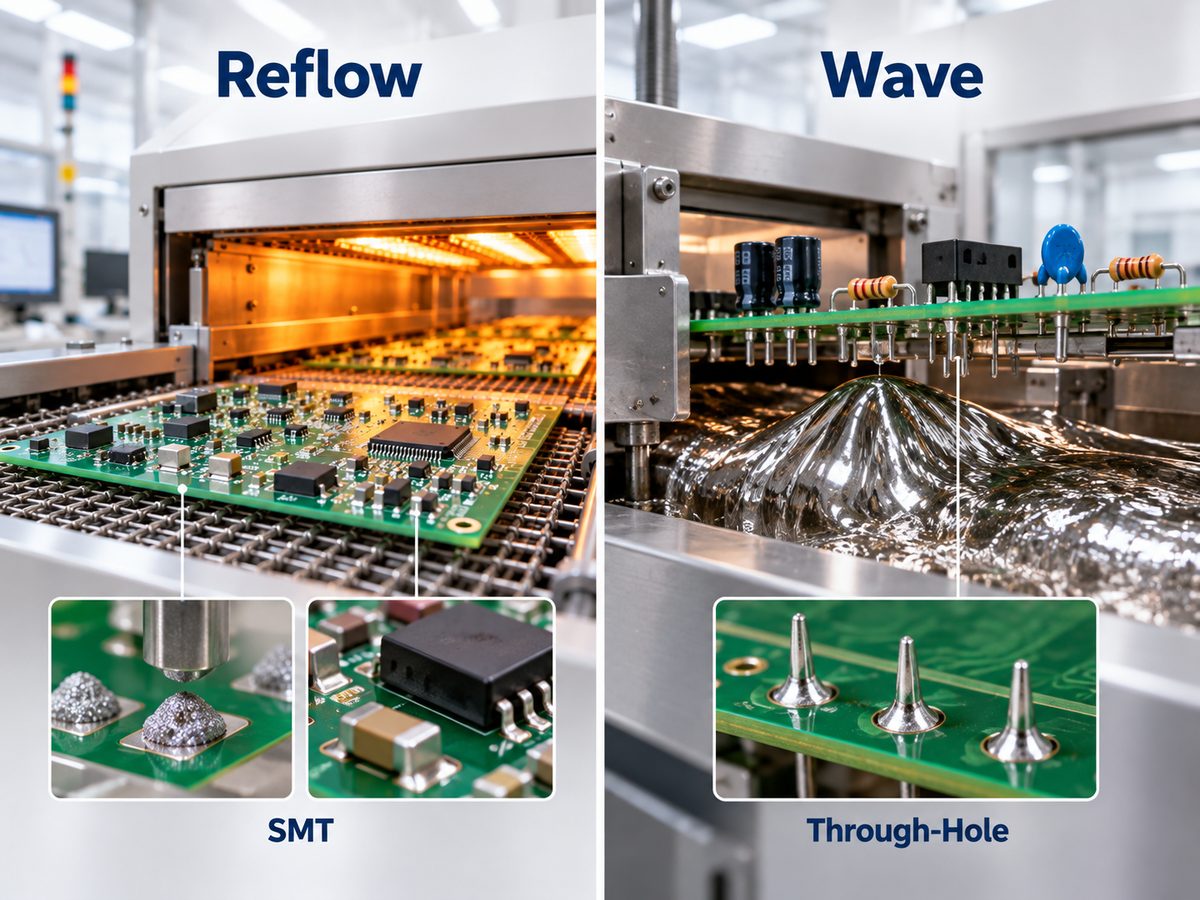
Why Choose EBest Circuit for Custom Pogo Pin PCB Assembly?

EBest combines PCB design, fabrication, component sourcing and assembly services, allowing you to purchase the carrier as a populated board. These services can support the following stages of your project:

  • Before the first build: Use PCB design support and a free DFM review to resolve footprint, hole and board-manufacturing questions. Supply the contact drawing and mating dimensions; a PCB manufacturability review does not replace mechanical qualification of the enclosure.
  • During prototyping: Order the carrier and any agreed mating board for evaluation with your hardware. Use the measured fit and electrical results to decide whether to revise pad size, support, contact selection or assembly requirements before a larger build.
  • For component procurement: Have sourcing follow the selected BOM, with alternatives identified for approval. Keeping the contact part number controlled helps prevent a purchasing substitution from changing compression or installation requirements.

  • When moving to production: Order against the accepted board revision, BOM and agreed inspection plan. Confirm the included boards, populated components, tooling and reports in the quotation. Complete fixture development and specialist reliability testing require separate confirmation.

FAQs About Pogo Pin PCB Assemblies

Q1: Is a six-pin pogo interface a standard pinout?

A1: No. Six is only the contact count. Define power, return and signal assignments, the viewing direction and a clear pin-one reference on both mating drawings. Check the reversed orientation as well as the intended one before approving the layout.

Q2: Should exposed charging contacts remain energized?

A2: That depends on the product’s protection design. Evaluate shorts from metal objects, incorrect mating and the connection sequence. Where needed, use current limiting or controlled power enable and test those functions with the actual dock; selecting a pogo pin does not provide this protection.

Q3: How should conformal-coating keepouts be specified?

A3: Mark the landing surfaces and moving-contact areas that must remain uncoated, including their location tolerances. Specify masking and inspect after coating. Protection applied over the contact surface can prevent conduction, while material entering the barrel can interfere with movement.

Q4: Can the completed carrier be washed?

A4: Only with a process permitted for the selected contact and other components. Confirm the chemistry, ingress restrictions and drying conditions before washing. Check plunger return and electrical behavior afterward; an externally clean board can still contain residue inside a moving contact.

Q5: Can a pogo pin be replaced by another part with the same pitch?

A5: Pitch alone is insufficient. Compare free and working heights, force curve, tip shape, mounting dimensions, electrical limits and process compatibility. Recalculate the gap and landing area where any of these differ, and approve the substitute before assembly.

Q6: Should a test fixture use replaceable probes?

A6: Replaceable probes can reduce maintenance rework in frequently used fixtures. Select a compatible probe and receptacle, provide removal access and identify the permitted replacement part. Verify seating and electrical performance after replacement rather than assuming any probe of the same diameter will work.

Q7: Does magnetic retention make the connection waterproof?

A7: No. Magnets provide retention, while seals and enclosure geometry control ingress. Check holding force at the real gap and evaluate sealing separately under the product’s required conditions. A magnet or gold-plated contact alone does not establish an ingress rating.

Start Your Custom Pogo Pin PCB Assembly Project

Send your PCB files, BOM with contact part numbers, mating drawing, quantities and test requirements to sales@bestpcbs.com. EBest Circuit can review the PCB manufacturing requirements and quote the agreed design, board supply, sourcing and assembly work. Include your required delivery date and the outstanding prototype checks so the next build answers the questions that still affect production.

You may also like

What Is an LCR Meter? Working Principle & How to Use It?

September 3rd, 2026

An LCR meter measures the electrical behavior of resistors, capacitors, inductors, coils, and other passive components under an AC test signal. Unlike a basic multimeter, it can show not only resistance or capacitance, but also impedance, ESR, Q factor, dissipation, and phase-related parameters.

That matters because real components are not ideal. A capacitor has resistance and parasitic inductance. An inductor has winding resistance and stray capacitance. Their measured values can change with frequency, fixture setup, temperature, and even the surrounding PCB circuit.

This guide explains how an LCR meter works, how to choose the right measurement settings, and how to use it for component and PCB testing.

LCR meter measuring capacitance, inductance, resistance, and PCB components

What Is an LCR Meter?

An LCR meter is an electronic instrument used to measure inductance (L), capacitance (C), and resistance (R).

The name comes from its three main parameters:

  • L — Inductance, measured in henries (H)
  • C — Capacitance, measured in farads (F)
  • R — Resistance, measured in ohms (Ω)

A digital LCR meter normally measures these parameters by applying a controlled AC signal rather than relying only on DC measurement.

This makes it useful for checking components whose electrical behavior changes with frequency, including:

  • ceramic and electrolytic capacitors;
  • inductors and chokes;
  • transformer windings;
  • precision resistors;
  • PCB coils and planar inductors.

For basic component identification, a simple handheld unit may be enough. More demanding laboratory or production measurements usually require tighter accuracy, controlled fixtures, and a wider test-frequency range.

What Does an LCR Meter Measure Besides L, C, and R?

L, C, and R are only the starting point. Many LCR meters also calculate secondary parameters that show how much loss or parasitic behavior a component has.

LCR meter measurement parameters including L, C, R, ESR, Q, D, and impedance
Parameter Meaning Typical Use
L Inductance Inductors, coils
C Capacitance Capacitors
R Resistance Resistors, winding resistance
Z Impedance Overall AC behavior
ESR Equivalent series resistance Capacitor loss
Q Quality factor Inductor performance
D Dissipation factor Capacitor loss
θ Phase angle Reactive behavior

For example, two capacitors may both measure close to 100 µF, yet one may have much higher ESR. In a power circuit, that difference can affect ripple, heating, and stability even though the capacitance reading looks acceptable.

Q factor is commonly used for inductors. It compares reactive behavior with resistive loss at a specified frequency. Dissipation factor performs a similar role for capacitors.

Because these values are frequency-dependent, an ESR or Q reading is much more useful when the test frequency is also recorded.

How Does an LCR Meter Work?

An LCR meter applies a known AC signal to the device under test and measures how the component responds.

How an LCR meter works using an AC signal, voltage and current measurement, phase difference, and impedance calculation

The measurement sequence is roughly:

  1. Generate an AC test signal.
  2. Apply it to the component.
  3. Measure voltage and current.
  4. Determine the phase difference between them.
  5. Calculate complex impedance.
  6. Convert the result into L, C, R, ESR, Q, D, or another selected parameter.

The AC signal is important because capacitors and inductors respond differently as frequency changes.

For a capacitor: Xc = 1 / (2πfC)

For an inductor: XL = 2πfL

As frequency rises, capacitive reactance falls while inductive reactance rises.

A more precise benchtop LCR meter may also use automatic balancing bridge techniques and four-terminal-pair connections. These methods reduce errors caused by test leads, contact resistance, and fixture parasitics.

Why Does Test Frequency Matter in LCR Measurements?

The same component can produce different LCR readings at different frequencies.

This is normal. Real components contain parasitic elements that become more or less significant as frequency changes.

Typical examples include:

  • Large electrolytic capacitors are often characterized at relatively low frequencies.
  • Small ceramic capacitors may be measured at 1 kHz or higher, depending on the specification.
  • Power inductors are commonly tested differently from small RF inductors.
  • An RF inductor can change behavior significantly as the test frequency approaches self-resonance.

A capacitor, for example, does not consist of capacitance alone. Its equivalent circuit also includes ESR and parasitic inductance. At low and moderate frequencies, capacitance may dominate. At sufficiently high frequencies, parasitic inductance becomes much more important.

For component acceptance testing, the best practice is simple:

Use the measurement frequency stated in the component datasheet or applicable test specification.

If the test is for troubleshooting rather than formal verification, choose a frequency relevant to the application and keep it consistent when comparing suspect and known-good components.

What Is the Difference Between Series and Parallel Measurement Modes?

Series and parallel modes are equivalent circuit models used to represent the losses in a real component.

Common settings include:

  • Cs — series capacitance
  • Cp — parallel capacitance
  • Ls — series inductance
  • Lp — parallel inductance
  • Rs — series resistance
  • Rp — parallel resistance

They do not mean that the physical component changes internally. The meter is simply expressing the same impedance using a different mathematical model.

As a practical rule:

  • Lower-impedance devices are often represented with a series model.
  • Higher-impedance devices are often represented with a parallel model.

The correct setting depends on the device, frequency, and test specification.

This becomes important when checking lossy capacitors or inductors. Cs and Cp, or Ls and Lp, may not give identical numerical results. If a datasheet specifies one equivalent model, use that same model during verification.

Handheld vs Benchtop LCR Meter: What Is the Difference?

The main difference is not simply portability. It is the amount of control the instrument gives over the measurement.

Comparison between handheld and benchtop LCR meters
Feature Handheld LCR Meter Benchtop LCR Meter
Portability High Low
Frequency range Usually narrower Usually wider
Accuracy General-purpose Higher precision
Fixtures Basic More options
Bias capability Limited More common
Automation Limited Often supported
Typical use Repair, field work R&D, QC, production

A handheld LCR meter is useful for:

  • maintenance;
  • component sorting;
  • quick incoming checks;
  • general troubleshooting.

A benchtop unit is more appropriate when a test requires:

  • tighter tolerances;
  • repeatable fixtures;
  • multiple test frequencies;
  • DC bias;
  • automated data collection;
  • production pass/fail limits.

The right choice depends on what needs to be measured, not on whether one instrument has more features.

LCR Meter vs Multimeter: What Is the Difference?

A multimeter is designed for general electrical troubleshooting. An LCR meter is designed to characterize passive components under controlled AC conditions.

A typical multimeter measures:

  • AC/DC voltage;
  • current;
  • resistance;
  • continuity;
  • diode behavior.

Some models also provide basic capacitance or frequency functions.

An LCR meter can usually measure:

  • inductance;
  • capacitance;
  • resistance;
  • impedance;
  • ESR;
  • Q factor;
  • dissipation factor;
  • phase angle.

It also allows the user to select test frequency and, on many models, the equivalent circuit.

For checking whether a 1 kΩ resistor is open, a multimeter is sufficient.

For determining whether an inductor still meets its inductance and Q requirements, or whether a capacitor has excessive ESR, an LCR meter gives much more useful information.

How to Use an LCR Meter?

A reliable LCR measurement depends on both the instrument settings and the test setup.

Step-by-step guide showing how to use an LCR meter

A practical workflow is:

  1. Power off the circuit. Passive LCR measurements should not normally be made on an energized circuit.
  2. Discharge capacitors. Stored charge can distort the reading or damage the meter input.
  3. Choose the correct fixture. SMD tweezers work well for small chip components. Kelvin clips or dedicated fixtures improve repeatability for low-impedance measurements.
  4. Perform open and short compensation. This reduces errors from leads, fixtures, stray capacitance, and residual impedance.
  5. Select the main parameter. Choose L, C, R, Z, or automatic detection if supported.
  6. Set the test frequency. Match the datasheet condition when verifying a rated value.
  7. Choose series or parallel mode. Use the mode specified for the component whenever possible.
  8. Connect the component securely. Poor contact can cause unstable or inflated readings.
  9. Read the secondary parameter as well. Capacitance plus ESR, or inductance plus Q, is often more informative than the primary value alone.
  10. Compare under the same conditions. Frequency, fixture, temperature, and circuit model should remain consistent between measurements.

For repeated inspection, document the meter settings in the test instruction. Otherwise two operators can test the same component and obtain different results simply because they used different frequencies or modes.

Can You Measure Components Directly on a PCB with an LCR Meter?

Yes, but an in-circuit reading may include the electrical effect of other components connected around the part.

LCR meter applications comparing in-circuit PCB screening with isolated component measurement

This is especially common with:

  • capacitors connected in parallel on a power rail;
  • resistors forming parallel current paths;
  • transformer or inductor windings connected to other circuitry;
  • semiconductor junctions;
  • passive filter networks.

Suppose several capacitors share the same supply rail. Measuring one capacitor without removing it may effectively measure part of the entire network rather than that single component.

In-circuit LCR measurements are still useful for quick screening. A technician may compare a suspect PCB with a known-good board and look for a major difference.

For an accurate standalone value, it may be necessary to:

  • lift one terminal;
  • remove the component;
  • isolate the surrounding circuit;
  • test the part in a dedicated fixture.

A strange in-circuit reading should therefore be treated as a diagnostic clue, not immediate proof that the component has failed.

What Causes Incorrect LCR Meter Readings?

Many incorrect readings come from the setup rather than the component itself.

Common causes include:

  • Wrong test frequency — the component is being measured under conditions different from its datasheet rating.
  • Wrong equivalent model — Cs/Cp or Ls/Lp selection changes the reported value.
  • No open/short compensation — lead and fixture parasitics become part of the result.
  • Poor contact — oxidized leads or unstable clips add resistance.
  • Long test leads — extra inductance and capacitance become significant.
  • In-circuit paths — nearby components alter the measured impedance.
  • Temperature change — many passive components have measurable temperature coefficients.
  • DC bias effects — some ceramic capacitors lose effective capacitance under applied bias.
  • Contamination — moisture, flux residue, or dirt can affect high-impedance and low-capacitance measurements.
  • Operating near the meter limits — accuracy usually falls when the component value is close to the instrument’s practical measurement range.

Fixture parasitics deserve particular attention when measuring very small capacitance or inductance. A few picofarads of stray capacitance may be negligible when measuring microfarads, but very significant when the DUT itself is only a few picofarads.

Low-resistance and low-inductance measurements similarly benefit from Kelvin or four-wire techniques because ordinary test-lead resistance can become comparable to the device being measured.

How Are LCR Meters Used in PCB and PCBA Testing?

LCR meters are useful in PCB and PCBA work when a simple resistance or continuity check does not provide enough information.

Typical applications include:

  • Incoming component inspection — verifying resistor, capacitor, and inductor values before assembly.
  • Capacitor troubleshooting — checking capacitance, ESR, or dissipation in unstable power circuits.
  • Inductor and coil verification — measuring inductance, winding resistance, and Q.
  • Transformer checks — comparing winding parameters with approved samples.
  • Alternative-part verification — confirming that a substitute passive component matches the required electrical behavior.
  • First-article troubleshooting — checking suspect components against BOM or datasheet requirements.
  • Failure analysis — identifying parameter drift after thermal or electrical stress.
  • Printed coil testing — measuring PCB inductors, planar coils, and similar structures after fabrication.

The measurement procedure should define more than a nominal component value.

For production or quality inspection, useful test requirements normally include:

  • test frequency;
  • allowable tolerance;
  • fixture type;
  • series or parallel mode;
  • secondary parameter limits where relevant.

For PCB coils, transformers, RF structures, and precision analog circuits, these conditions are especially important because parasitic behavior is part of the real electrical performance.

FAQs About LCR Meters

What does LCR stand for on a meter? LCR stands for inductance, capacitance, and resistance. These are the three primary passive-component parameters measured by the instrument.

Can an LCR meter measure ESR? Yes, many digital LCR meters can measure or calculate equivalent series resistance. ESR is commonly used when evaluating capacitor loss.

Why does capacitance change when I change the test frequency? Real capacitors contain ESR, dielectric losses, and parasitic inductance. Their combined impedance changes with frequency, so the calculated capacitance may also change.

Is an LCR meter better than a multimeter for testing capacitors? For detailed capacitor characterization, usually yes. An LCR meter can measure capacitance together with ESR, dissipation, and frequency-dependent behavior that a basic multimeter cannot show.

Can I test a capacitor without removing it from the PCB? You can perform an in-circuit screening test, but parallel components may influence the reading. Isolate or remove the capacitor when an accurate standalone value is required.

What frequency should I use on an LCR meter? Use the frequency specified in the component datasheet when checking compliance with a rated value. For troubleshooting, use a frequency appropriate to the application and keep it consistent between comparisons.

How Can EBest Circuit Support Your PCB and PCBA Project?

If you need PCB or PCBA manufacturing support involving passive-component verification, printed coils, electrical testing, or assembly troubleshooting, send your Gerber files, BOM, and test requirements to sales@bestpcbs.com.

You may also like

What Is Lead Free Solder Material? A PCB Assembly Guide

September 3rd, 2026

Lead free solder material is a tin-based alloy used to create electrical and mechanical connections without intentionally adding lead. Common PCB assembly choices include SAC305, tin-copper alloys, low-silver SAC alloys, and low-temperature tin-bismuth alloys. They differ in composition, melting behavior, wetting, mechanical response, process temperature, and cost.

For PCB buyers, “lead free” alone is not a complete solder specification. The alloy should match the assembly method, component temperature limits, PCB surface finish, reliability target, and regulatory requirements.

Lead free solder material used in PCB assembly, including solder wire, paste and bar

What Is Lead Free Solder Material?

Lead free solder material is a solder alloy in which lead is not intentionally used as the primary alloying element and which meets the applicable lead-content requirement for the product. Most electronic lead-free solders use tin as the base metal, combined with silver, copper, bismuth, nickel, or other elements.

A common example is SAC305, which contains approximately 96.5% tin, 3.0% silver, and 0.5% copper.

Lead-free solder can be used for:

  • SMT reflow soldering
  • Wave soldering
  • Selective soldering
  • Hand soldering and rework
  • BGA and other area-array interconnections

“Lead free” does not describe one fixed alloy. Different lead-free solder materials can have very different melting temperatures and process behavior.

What Is Lead Free Solder Made Of?

Most lead-free electronic solders are based on tin, with smaller amounts of other metals added to adjust melting temperature, strength, wetting, intermetallic formation, or solder-pot behavior.

  • Tin (Sn) is normally the base metal.
  • Silver (Ag) influences strength and SAC solder-joint microstructure. Higher silver content also increases material cost.
  • Copper (Cu) affects intermetallic formation and solder-pot behavior.
  • Bismuth (Bi) lowers melting temperature and is widely used in low-temperature solder systems.
  • Nickel (Ni) may be added in small amounts to modify intermetallic behavior in some SnCu alloys.
  • Germanium (Ge) and similar micro-alloy additions may help control oxidation and dross.

The required alloying elements depend on the soldering process and reliability target rather than on one metal being universally better than another.

What Are the Composition Percentages of Common Lead-Free Solder Alloys?

Lead free solder material composition varies by process and reliability target, with SAC305 serving as the most familiar reference.

Comparison of common lead-free solder compositions including SAC305, SAC405, SnCu and SnBi
Lead-Free Alloy Typical Composition by Weight Melting Behavior Typical Application
SAC305 Sn 96.5%, Ag 3.0%, Cu 0.5% 217–220°C General SMT and reflow
SAC405 Sn 95.5%, Ag 4.0%, Cu 0.5% 217–225°C Higher-silver SAC applications
Sn99.3Cu0.7 Sn 99.3%, Cu 0.7% About 227°C Wave soldering and cost-sensitive production
Sn42Bi58 Sn 42%, Bi 58% About 138°C Low-temperature assembly
Low-Ag SAC Sn-based with reduced Ag and Cu Alloy dependent Cost-sensitive and application-specific assembly

For procurement, specify the exact alloy designation when the solder composition is controlled by the drawing, qualification plan, or customer specification.

What Is the Melting Point of Lead-Free Solder?

Lead-free solder does not have one fixed melting point. The temperature depends on the alloy composition.

Typical values include:

  • SAC305: approximately 217–220°C
  • SAC405: approximately 217–225°C
  • Sn99.3Cu0.7: approximately 227°C
  • Sn42Bi58: approximately 138°C
  • Sn63Pb37, for comparison: 183°C
Lead-free solder melting point comparison chart

Melting temperature, soldering-iron temperature, and reflow peak temperature should not be confused.

SAC305 becomes fully liquid around 220°C, but a production reflow process typically peaks around 240–250°C, depending on solder paste specifications, PCB thermal mass, component limits, and required time above liquidus.

For heat-sensitive connectors, LEDs, flex circuits, plastics, batteries, or temperature-sensitive components, the thermal limit should be reviewed before selecting the solder alloy.

What Material Properties Matter in Lead-Free Solder?

The most relevant solder properties are those that affect manufacturability and long-term joint performance.

  • Wetting behavior: affects solder spread, fillet formation, hole fill, and process margin.
  • Mechanical strength: matters where solder joints experience vibration, shock, or handling loads.
  • Ductility and creep: affect how the joint responds to sustained mechanical and thermal strain.
  • Thermal-fatigue behavior: matters in applications exposed to repeated temperature cycling.
  • Intermetallic formation: affects the interface between solder and copper or component finishes.
  • Electrical and thermal properties: matter in current-carrying and thermally demanding joints.
  • Oxidation and dross behavior: are especially relevant in wave and selective soldering.

These properties should be evaluated against the actual component package and operating environment.

How Does Lead-Free Solder Compare With Lead Solder?

A useful electronics comparison is leaded vs lead free solder, especially SAC305 versus traditional Sn63Pb37.

Factor SAC305 Lead-Free Sn63Pb37 Leaded
Nominal composition Sn96.5Ag3.0Cu0.5 Sn63Pb37
Melting behavior 217–220°C 183°C
Process temperature Higher Lower
Wetting behavior Generally less forgiving Generally easier
Joint appearance Often duller Typically brighter
Regulatory use Common in RoHS-compliant products Restricted unless exempt
Current electronics use Mainstream Legacy and specialized applications

The higher thermal exposure of SAC305 can affect laminate durability, component moisture sensitivity, connector plastics, warpage, and overall process margin.

When converting an older SnPb assembly to lead-free production, the PCB and component set should be checked for lead-free reflow compatibility.

Is Lead Free Solder Really Lead Free?

“Lead free” does not necessarily mean that laboratory analysis must detect exactly 0.000% lead.

Under EU RoHS, the general maximum concentration value for lead is 0.1% by weight in a homogeneous material, unless a relevant exemption applies.

This matters when reviewing:

  • alloy certificates
  • RoHS declarations
  • recycled solder
  • mixed-process production
  • legacy components
  • contaminated solder pots

A purchase order should state the required compliance standard rather than relying only on the phrase “lead-free solder.”

What Forms Does Lead-Free Solder Come In?

The alloy and the product form are separate specifications.

Lead-free solder forms including paste, wire, bar, spheres, preforms and powder
Solder Form Typical Use
Lead-free solder paste SMT stencil printing and reflow
Lead-free solder wire Hand soldering and rework
Lead-free solder bar Wave and selective soldering
Solder spheres BGA and CSP packages
Solder preforms Controlled solder-volume applications
Solder powder Main metallic constituent of solder paste

Lead-free solder paste is not simply another name for lead-free solder alloy. Paste combines solder powder with flux and other constituents needed for printing and reflow.

For soldering wire material, buyers may also need to specify wire diameter, flux type, flux percentage, and alloy.

For solder bar, solder-pot volume, dross generation, copper dissolution, contamination control, and alloy cost become more important.

Which Lead-Free Solder Material Is Best for PCB Assembly?

There is no single best alloy for every assembly. SAC305 is a common starting point, but the soldering method and thermal constraints should drive selection.

Lead-free solder selection guide for SMT, wave soldering, heat-sensitive assembly, rework and thermal cycling
Assembly Requirement Typical Starting Point Reason
General SMT reflow SAC305 Mature and widely supported process
Mixed SMT and through-hole PCBA SAC305 or compatible SAC system Easier alloy consistency
High-volume wave soldering SnCu or low-Ag alloy Lower silver cost
Heat-sensitive assembly SnBi-based alloy Lower process temperature
Hand soldering and rework SAC or SnCu flux-cored wire Practical manual application
Severe thermal cycling Application-qualified alloy Reliability must be validated
Legacy SnPb conversion Process review required Components and PCB may not tolerate lead-free conditions

Low-temperature SnBi alloys can reduce thermal exposure, but mechanical requirements, alloy mixing, and rework conditions still need review.

At EBest Circuit, PCBA quotation and process review are easier when customers provide the BOM, PCB files, required solder alloy, compliance requirement, temperature limits, assembly method, and expected production volume.

What Standards Apply to Lead-Free Solder Materials?

Different standards apply to solder alloys, paste, flux, workmanship, and substance restrictions.

Standard / Regulation Main Relevance
IPC J-STD-006 Electronic-grade solder alloys and solid solders
IPC J-STD-005 Solder paste requirements
IPC J-STD-004 Soldering flux classification and requirements
IPC J-STD-001 Requirements for soldered electronic assemblies
EU RoHS Restrictions on lead and other regulated substances

RoHS compliance does not replace workmanship or process-control requirements.

The required standard revision should also be checked against the drawing, customer specification, or contract rather than assumed automatically.

What Reliability Issues Should Engineers Consider With Lead-Free Solder?

Lead-free solder reliability depends on the alloy, package, PCB construction, operating environment, and dominant failure mechanism.

Key issues include:

  • Thermal cycling: repeated CTE mismatch strains solder joints.
  • Intermetallic growth: interface layers continue to evolve during thermal exposure.
  • Copper dissolution: relevant in prolonged wave and selective soldering.
  • Voiding: important under QFNs, BTCs, power packages, and thermal pads.
  • Drop and vibration loading: relevant to portable and mechanically stressed products.
  • High operating temperature: increases the importance of creep and microstructural evolution.
  • Mixed alloys: can change local composition, melting behavior, microstructure, and compliance status.

For reliability-sensitive projects, provide the expected operating temperature range, thermal-cycle requirement, vibration or drop conditions, major package types, board thickness, surface finish, and target product life.

What Are Acceleration Factors for Lead-Free Solder Materials?

Acceleration factors for lead free solder materials estimate how much faster solder-joint damage accumulates during an accelerated reliability test than under expected field conditions.

For thermal cycling, the result can be influenced by:

  • temperature range
  • maximum and minimum temperature
  • dwell time
  • ramp rate
  • cycle frequency
  • PCB and package geometry
  • CTE mismatch
  • solder-joint dimensions
  • alloy creep and fatigue behavior

Coffin-Manson- and Norris-Landzberg-type models may be used for thermal-fatigue analysis, but the model assumptions and parameters should match the actual assembly.

Acceleration factors developed for SnPb joints or for one package type should not be transferred directly to another lead-free assembly without validation.

FAQs About Lead Free Solder Material

What is the most common lead-free solder for PCB assembly?

SAC305 is one of the most widely used general-purpose lead-free alloys. Its nominal composition is Sn96.5Ag3.0Cu0.5, with a melting range of approximately 217–220°C.

Is 60/40 solder lead free?

No. Traditional 60/40 solder contains approximately 60% tin and 40% lead.

Why does lead-free solder require a higher soldering temperature?

Common SAC and SnCu alloys melt at higher temperatures than Sn63Pb37. SAC305 melts around 217–220°C, compared with 183°C for Sn63Pb37.

Does lead-free solder need flux?

Yes. Flux helps remove surface oxides and improves solder wetting. The flux chemistry should match the soldering process and cleanliness requirements.

Can leaded and lead-free solder be mixed?

They can physically mix, but uncontrolled mixing can alter alloy composition, melting behavior, microstructure, process consistency, and regulatory compliance.

Is SAC305 suitable for wave soldering?

Yes. SAC305 can be used for wave soldering, although SnCu or lower-silver alloys may be considered for high-volume production where solder-pot cost matters.

Should a PCB drawing specify the exact solder alloy?

Yes, when the alloy is part of the approved process or reliability qualification. Otherwise, specify the required lead-free or RoHS status and applicable assembly standard.

How Can EBest Circuit Support Lead-Free PCB Assembly?

Lead-free solder selection should match the PCB assembly process, component temperature limits, reliability requirements, and compliance target. SAC305 is suitable for many assemblies, while SnCu, low-silver SAC, and SnBi alloys serve more specific process needs.

For a PCBA quotation, send your Gerber files, BOM, assembly drawings, production volume, required solder alloy, RoHS requirement, and any temperature or reliability constraints to EBest Circuit at sales@bestpcbs.com.

You may also like