PCB manufacturing PCB manufacturing
Home > Blog

power supply PCB

What Is a Rectifier Diode and How Does It Work?
Tuesday, September 15th, 2026

A rectifier diode is a semiconductor component that conducts mainly in one direction and blocks reverse current within its voltage rating. It is used to turn AC into a unidirectional, pulsating output. On a PCB, its performance depends on more than the part number: current, switching speed, polarity, copper paths and cooling must work together.

Rectifier diode concept illustration showing axial and surface-mount packages on a PCB

What Is a Rectifier Diode?

A rectifier diode is a diode selected for power rectification rather than primarily for processing small signals. Its two terminals are the anode and cathode. An individual diode is a component; a diode rectifier can be a complete circuit containing several devices, or an integrated bridge package.

In a PCB power supply, rectification is only one stage. Filtering reduces ripple, and a regulator controls the output voltage. A diode alone does not provide a smooth, regulated supply or electrical isolation.

How Does a Rectifier Diode Work?

The rectifier diode function follows its bias condition. With sufficient forward bias, conventional current flows from anode to cathode. Reverse bias greatly reduces that current, but leakage remains; exceeding the device’s reverse-voltage capability can damage it.

What does a rectifier diode do when the input alternates? In a simple series circuit, it passes one half-cycle and blocks the other. Arranging multiple devices into a full-wave circuit lets both input half-cycles deliver current through the load in the same direction.

Forward voltage is not a fixed 0.7 V. It changes with current, temperature and diode technology. A PN device also takes time to remove stored charge when switching from conduction to blocking, so a diode that suits a low-frequency supply may be unsuitable in a switching converter.

What Does the Rectifier Diode Symbol Mean?

The rectifier diode symbol identifies the anode and cathode; the straight bar marks the cathode. On many axial rectifiers, a band on the body identifies that same terminal. Match the symbol, package drawing and PCB footprint before assigning placement orientation. The rectifier diode diagram below relates the physical band to the two terminals.
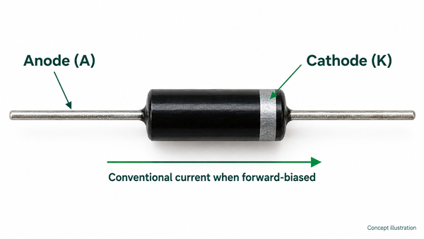
Rectifier diode diagram relating the axial cathode band to anode and cathode terminals

A rectifier diode number such as 1N4007 identifies an electrical device family, not a complete footprint specification. Supplier suffixes can change packaging and lead details. For SMD parts, confirm the manufacturer marking drawing rather than relying on a stripe convention alone. A readable polarity mark on the assembly drawing helps prevent a correct component being fitted backward.

How Do Half-Wave and Full-Wave Rectifier Circuits Differ?

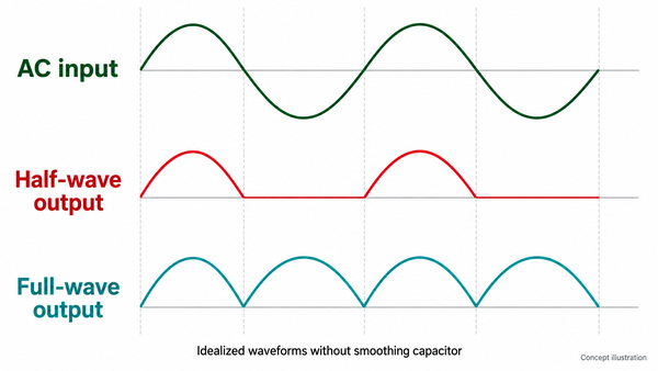
A half-wave circuit uses one input half-cycle; a full-wave circuit uses both. In a single-phase rectifier diode circuit, the common full-wave choices are a four-diode bridge or a two-diode circuit with a center-tapped transformer secondary.

CircuitDiodes and sourceEffect on the load
Half-waveOne diode with an AC sourceOne pulse per input cycle; larger gaps between charging pulses
Full-wave bridgeFour diodes; no center tap requiredTwo pulses per cycle; two diodes conduct in series in each current path
Center-tapped full-waveTwo diodes and a center-tapped secondaryTwo pulses per cycle; each half-secondary conducts on alternate half-cycles
Conceptual comparison of AC input, half-wave output and full-wave output without a smoothing capacitor

How Many Diodes Are Used in a Bridge Rectifier?

A single-phase diode bridge rectifier uses four diodes. Its two alternating current paths each contain two conducting devices. This full wave bridge rectifier arrangement is convenient, but its two forward drops can be significant on a low-voltage rail.

In half wave rectifier diode selection, account for the interval in which the load receives no input energy. In full wave rectifier diode selection, consider which winding and diode pair carry current at each instant. A bridge rectifier diode must handle the charging pulses as well as the reverse-blocking interval.

A smoothing capacitor changes the current waveform: the diodes recharge it in pulses near the AC peaks. Diode peak current can therefore be much higher than the average load current. Ripple and inrush must be considered together, not solved by choosing a larger capacitor alone.

Which Rectifier Diode Types Suit Your Circuit?

Rectifier diode types differ in switching behavior and losses. Start with the circuit frequency and reverse voltage, then compare forward loss, leakage and package cooling.

TechnologyTypical fitMain selection trade-off
Standard silicon PN rectifierLow-frequency AC rectificationLow cost, but recovery may be too slow for a switching stage
Fast or ultrafast PN rectifierSwitching power conversionRecovery charge and softness must be weighed against forward loss
Silicon Schottky rectifierLow-voltage rails and fast switchingLow forward loss can be useful; reverse leakage rises with temperature
SiC Schottky rectifierHigher-voltage, high-frequency conversionAssess switching loss, conduction loss, cost and thermal design together

Rectifier Diode vs Diode: What Is the Difference?

A rectifier is one use of a diode, not a separate opposite category. A small-signal switching diode is optimized for a different combination of current, capacitance and speed. A silicon rectifier diode cannot be replaced safely just because another diode has the same outline.

Rectifier Diode vs Schottky Diode

A Schottky rectifier diode is itself a rectifier. Compared with a conventional PN part, a silicon Schottky device often offers lower forward voltage and avoids minority-carrier storage recovery, but capacitive switching current still exists. Verify leakage at the expected temperature rather than assuming the lowest forward drop always produces the coolest design.

How Do You Distinguish Between Zener Diode and Rectifier Diode Functions?

A Zener diode is designed to operate in controlled reverse breakdown for voltage-reference or clamping tasks. A conventional rectifier normally works in forward conduction and reverse blocking. Swapping these roles without checking ratings can destroy the device or stop the circuit working.

Is 1N4007 a Rectifier Diode?

Yes. The 1N4007 rectifier diode is a common general-purpose silicon PN rectifier. A representative DO-41 version has a 1,000 V repetitive peak reverse-voltage rating and a 1 A average forward-current rating, with the current rating tied to specified mounting and temperature conditions.

For this DO-41 example, the 1 A condition uses 9.5 mm leads at 75°C ambient; maximum forward voltage is 1.1 V at 1 A under the stated electrical test conditions. These are device limits, not a promise that any small PCB can deliver a continuous 1 A DC output. Check the exact manufacturer’s datasheet, derating curve and rectifier circuit before substitution.

Its familiar part number does not make it the default for high-frequency rectification. Standard recovery, package dissipation and surge loading may matter more than its high reverse-voltage rating.

How Do You Select Rectifier Diode Ratings?

Select the device against the actual circuit waveform and temperature, not just the nominal supply voltage. The key ratings answer different questions.

ParameterWhat to check
VRRMWorst repetitive reverse voltage, including circuit topology and expected transients; do not compare only with AC RMS voltage
IF(AV)Average forward current under the specified cooling, waveform and temperature conditions
IFSMNon-repetitive surge capability for the stated waveform and duration; not a continuous operating rating
VFForward loss at operating current and junction temperature
IRReverse leakage at operating voltage and temperature
trr and QrrReverse recovery time and charge under comparable test conditions
Tj and thermal resistanceAllowable junction temperature and the actual path from device to board, enclosure or heatsink

For a simple conduction-loss estimate, average the instantaneous product of diode voltage and current over time. Using VF × average current can be a first approximation when VF is represented appropriately; it does not include recovery or reverse-leakage losses. High-frequency designs need those additional terms.

Rectifier diode price also depends on package, qualification, voltage class and order quantity. A lower component cost is not a saving if it requires more cooling, a larger board or a different assembly process.

How Should Rectifier Diodes Be Laid Out on a PCB?

Give the rectifier a short current path, adequate copper and an unambiguous footprint. The board must carry pulsed current and remove heat without compromising insulation spacing.

For many control and low-power supply designs, FR4 printed circuit boards provide the required routing and mechanical support. Size conductors for the actual current waveform, copper thickness, allowable temperature rise and surrounding layout. Minimum fabrication line width is not a power-trace recommendation.
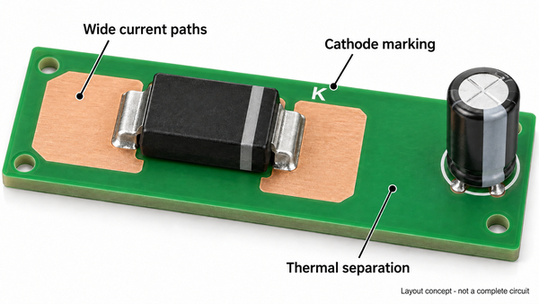
Conceptual PCB rectifier layout highlighting wide copper paths, polarity markings and separation from heat-sensitive capacitors
  • Keep the bridge-to-reservoir-capacitor charging loop compact, including its return path.
  • Use the specified land pattern and thermal-pad connection; do not add copper that bridges different electrical nodes.
  • Separate hot rectifiers from electrolytic capacitors and temperature-sensitive circuitry where practical.
  • Determine clearance and creepage from working voltage, environment and the applicable product requirements; do not use one spacing for every supply.
  • Make the cathode orientation consistent across schematic, silkscreen, assembly drawing and placement data.

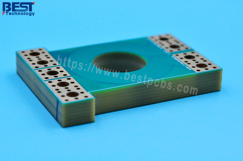
For higher-current paths, our heavy copper PCBs provide 4–10 oz copper options, subject to review of the complete design. Thicker copper can help current distribution and heat spreading, but it does not remove the diode’s junction-temperature limit. Wider conductors, pad geometry and soldering heat demand must be considered together.

How Do You Test a Rectifier Diode?

A multimeter’s diode mode can reveal a gross short or open circuit, but it does not prove the device will meet its high-voltage, current or switching ratings. Disconnect power, safely discharge stored energy and verify that no voltage remains before testing. Mains-connected supplies require qualified handling.

  1. With the isolated diode in forward bias, connect the red probe to the anode and the black probe to the cathode.
  2. Read the forward-voltage indication and compare it with the expected device technology and the meter’s test conditions.
  3. Reverse the probes. A normal reverse-blocking result usually appears as an over-range indication.
  4. If the result is ambiguous in circuit, isolate a terminal using an appropriate rework procedure; parallel paths can mislead the reading.

A near-zero reading both ways can indicate a short. Over-range both ways can indicate an open diode, but poor contact or insufficient meter test voltage can produce a similar result. Board-level diagnosis should also check solder joints, polarity and the surrounding circuit. A successful diode-mode reading does not replace a powered functional test under controlled conditions.

What Happens When a Diode Shorts in a Bridge Rectifier?

A shorted diode can create a heavy fault-current path during part of the AC cycle, potentially operating a fuse or damaging other components. Disconnect the supply and investigate the bridge and surrounding circuit before replacing parts; do not keep energizing the board to see whether the fault clears.

How Do We Build PCBs for Rectifier Circuits?

At EBest Circuit (Best Technology), we manufacture the PCB and assemble the specified components into your power-conversion circuit. Our PCB assembly services cover SMT, through-hole and mixed assembly, so an axial rectifier, an SMD diode and larger connectors can be incorporated into one board build.

We check incoming components against your BOM and support inspection and functional testing as part of the agreed assembly scope. Provide the exact diode part number, board files, polarity information and operating requirements so we can review the build consistently. Component selection remains tied to the approved design; we do not substitute a familiar diode number solely because the footprint fits.

For your next rectifier diode PCB project, send the fabrication files, BOM and assembly drawings to sales@bestpcbs.com. We can help connect the required copper construction, component mounting and assembly requirements in one manufacturing review.


You may also like

What is PCBA board for 12V adapter?
Friday, January 10th, 2025

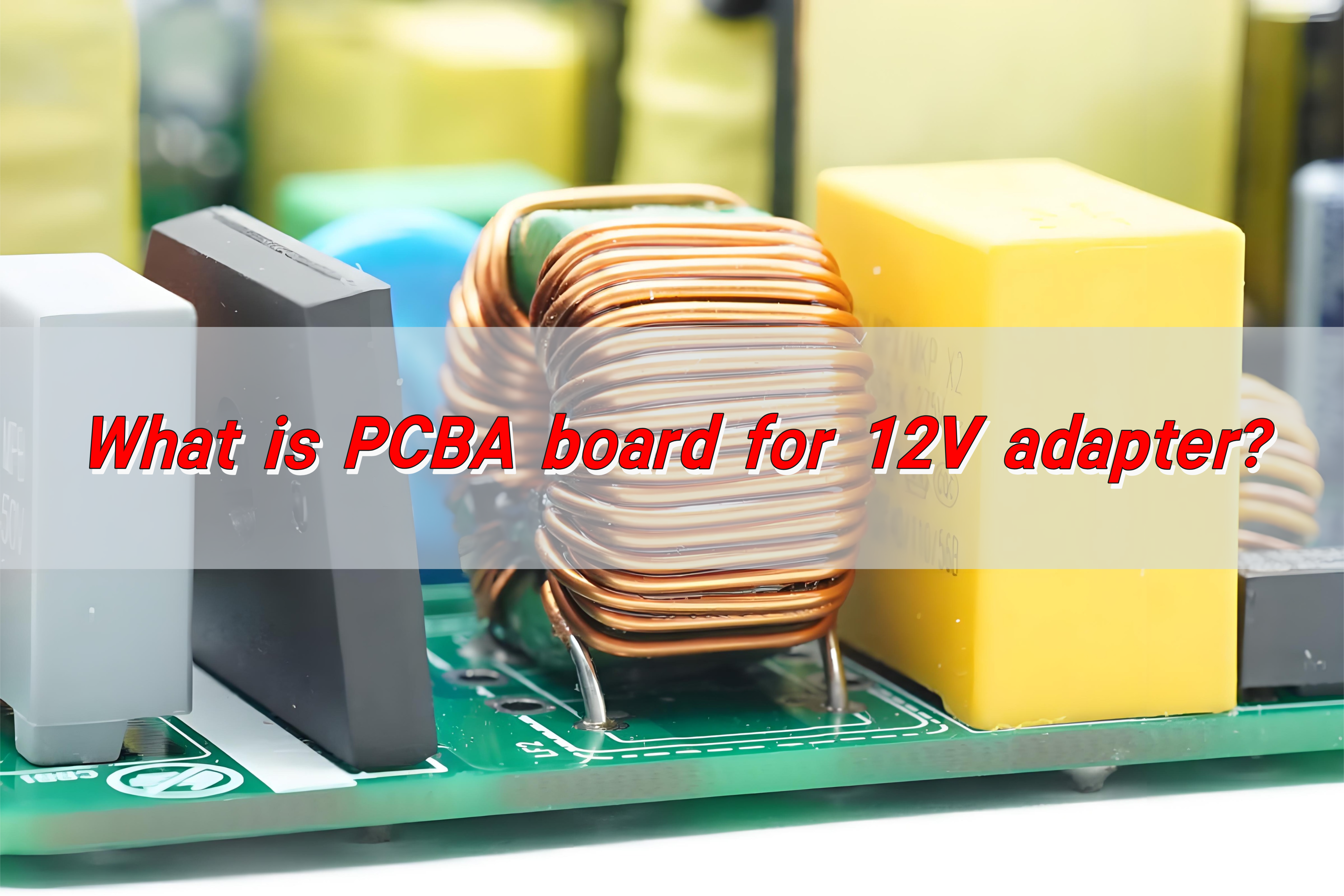
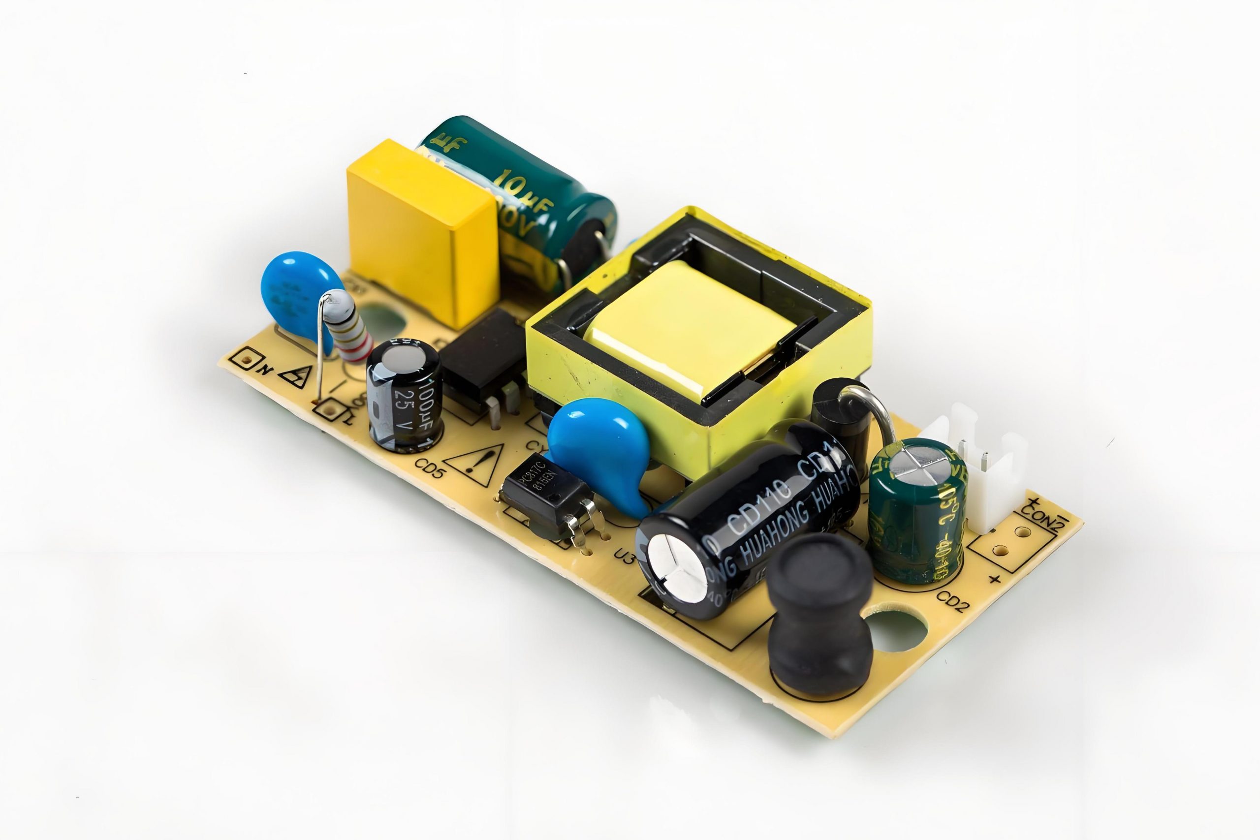
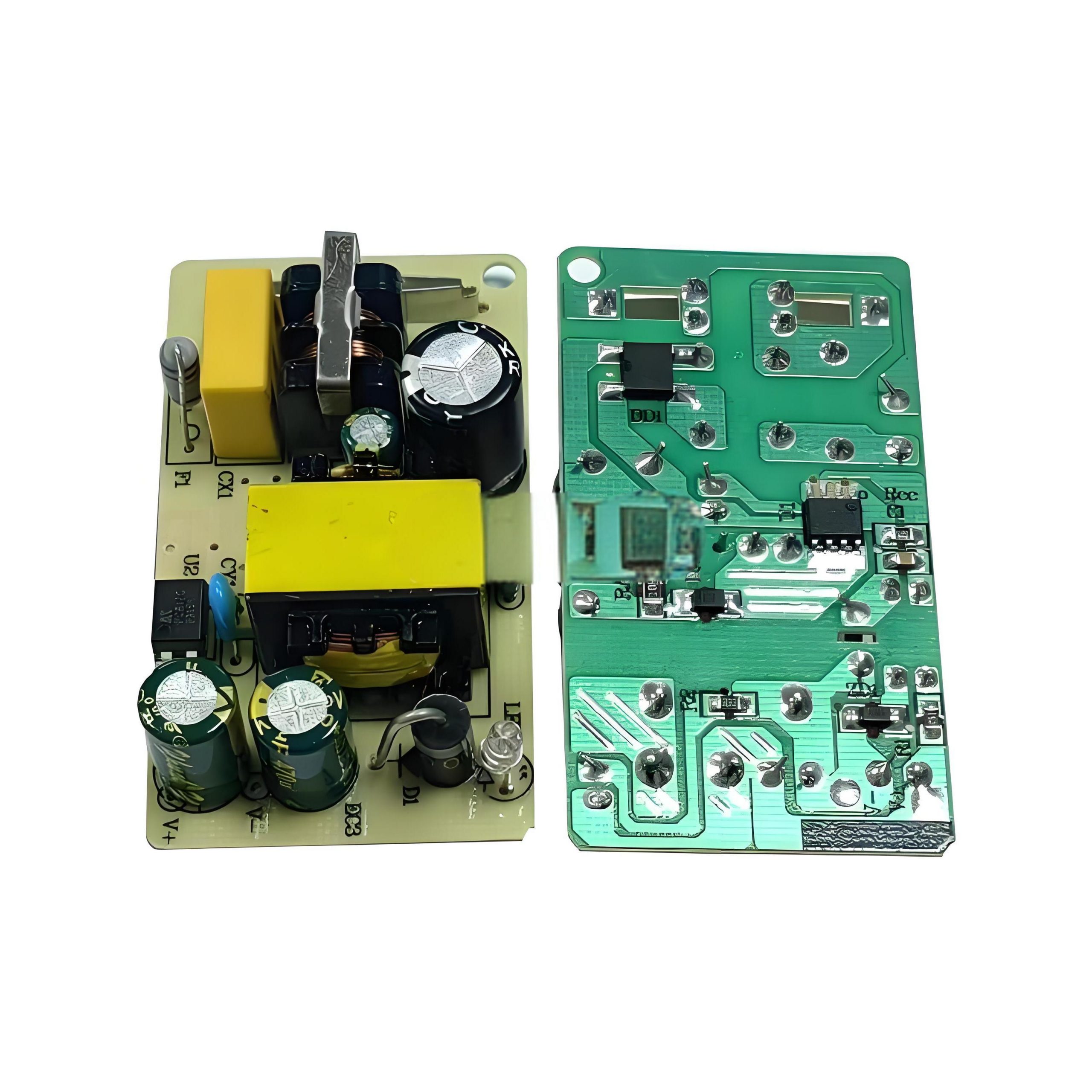
What is PCBA Board for 12V Adapter? The PCBA board of the 12V adapter is a circuit board assembly product that converts 220V AC power into 12V DC power. It is composed of PCB and various electronic components, including input terminals, transformers, rectifier bridges, filter capacitors, voltage regulator modules, output terminals, feedback circuits, and protection circuits. These components are connected to the PCB through solder to achieve stable voltage output and multiple protection functions.

What is a Power Supply PCB?

A power supply PCB is the heart of any electronic power system. It is the printed circuit board that manages the conversion of electrical energy from one form to another—usually from AC (Alternating Current) to DC (Direct Current). These boards are designed to handle specific power requirements, ensuring that voltage and current are regulated correctly for the devices they power.

For instance, a typical 12V adapter is designed to convert the electrical supply from a wall outlet (usually 110V or 220V AC) into a stable 12V DC that can safely power electronics such as routers, chargers, and small appliances. The power supply PCB in this adapter ensures the right voltage and current flow to the device, protecting both the adapter and the device being powered.

How to Design a Power PCB?

Designing a power PCB for an adapter, especially a 12V model, involves several considerations to ensure efficiency, safety, and durability.

  • Component layout: put related components together to reduce the length and interference of high-impedance lines; small signal lines are kept away from large current lines; heating components are kept away from temperature-sensitive components; the layout of adjustable components takes into account the requirements of the overall structure.
  • Unit circuit layout: arrange the positions of functional circuit units according to the circuit flow to ensure smooth signal flow; layout with core components as the center, and arrange components evenly, neatly and compactly; high-frequency circuits consider the distribution parameters of components, and general circuits arrange components in parallel.
  • Avoid interference: avoid adjacent parallel input and output wires, and add ground wires between wires to prevent feedback coupling.
  • Line width selection: determine the line width according to the current size, such as 50μm thick copper foil, 1mm wide can flow 1A current, and the temperature rise does not exceed 3℃; 2 ounces thick copper foil, 1mm wide can flow 1.5A current, and the temperature rise does not exceed 3℃.
  • Electrical clearance: The electrical clearance width between small current lines and output lines is generally 0.75mm – 1.0mm (minimum 0.3mm).
  • Cornering treatment: The routing corners are arc-shaped, avoiding right angles and sharp angles to avoid affecting the electrical performance of high-frequency circuits.
  • Power line treatment: According to the current size, the width of the power line is thickened to reduce the loop impedance, so that the direction of the power line and the ground line is consistent with the data transmission direction, the surrounding area is reduced, and the anti-noise ability is enhanced.

What is a PCB Adapter?

A PCB adapter refers to a circuit board that adapts one type of connection or interface to another. It is a crucial part of many electronic devices, especially when different voltage levels or types of connectors are involved.

What is PCBA board for 12V adapter?

In the context of a 12V adapter, the PCB serves as the central unit that converts the AC input (usually from the power outlet) into a regulated 12V DC output. This adapter PCB ensures that the power supplied to the device is stable and reliable, ensuring optimal performance.

What Does the PCBA Board for 12V Adapter Consist Of?

A typical PCBA board for a 12V adapter consists of several essential components. These components work together to ensure that the adapter provides stable, efficient, and safe power to connected devices. Here are the key elements:

  • Input Stage: This is where the AC voltage from the wall socket enters the adapter. It typically consists of a rectifier, which converts AC to DC. The rectifier often includes diodes that allow current to flow in only one direction, effectively converting the incoming AC into pulsed DC.
  • Filter Capacitors: After rectification, the DC signal can be uneven. To smooth out the waveform and make it stable, capacitors are used. These filter capacitors remove high-frequency noise and provide a smooth, steady DC voltage.
  • Voltage Regulator: A crucial component of the 12V adapter, the voltage regulator ensures that the output voltage remains constant at 12V, regardless of fluctuations in input voltage or changes in load. Linear regulators or switch-mode regulators may be used, depending on the efficiency required.
  • Inductors: Inductors help manage power flow by storing energy in a magnetic field. They play a role in smoothing the current flow and filtering high-frequency noise.
  • Output Stage: After the voltage is regulated, it passes through an output stage that provides the final output voltage. This stage may include protection features such as over-voltage and over-current protection to prevent damage to the adapter or the device it’s powering.
  • Heat Sink: To manage heat generated by the power conversion process, heat sinks are often attached to components that generate significant heat, such as voltage regulators. This helps to maintain safe operating temperatures.
  • Protection Circuits: To protect the adapter and the connected devices, protection circuits are included. These may consist of fuses, over-voltage, and over-current protection, ensuring the adapter doesn’t cause damage in case of electrical faults.

How to Manufacture PCBA Board for 12V Adapter?

Manufacturing a PCBA board for a 12V adapter is a multi-step process that requires precision and attention to detail. Here’s how it typically works:

  • Design and Prototyping: The first step is designing the PCB layout and schematic. This prototype is tested to ensure that the design works as expected.
  • PCB Fabrication: After finalizing the prototype, the design moves to the PCB fabrication stage. Here, the PCB material (usually fiberglass or epoxy resin) is used to create the physical board. The copper layers are etched to form the required circuit paths.
  • Component Sourcing: The next step is sourcing the components, including resistors, capacitors, voltage regulators, and diodes. Components are carefully chosen based on their specifications and compatibility with the design.
  • Soldering and Assembly: Once the components are sourced, they are placed on the PCB and soldered. This can be done manually or using automated machines in a process known as Surface Mount Technology (SMT).
What is PCBA board for 12V adapter?
  • Inspection and Testing: After assembly, the PCBA undergoes thorough testing to ensure it meets the required standards. This includes checking for shorts, open circuits, voltage stability, and functionality. Any defects are identified and corrected.
  • Final Assembly and Packaging: Once the PCBA passes all tests, it’s assembled into the final product. For a 12V adapter, this could mean placing the board into a casing and adding the necessary connectors for the input and output. The product is then packaged and ready for shipment.

How to Give Power Supply to PCB?

Providing power to a PCB is a straightforward process, but it requires care to ensure that the right voltage and current are supplied. Here’s how you typically provide power to a PCB:

  • Power Input: The power source, such as a wall outlet or battery, is connected to the PCB through the input pins. For a 12V adapter, the input will usually come from a 110V or 220V AC source.
  • Voltage Conversion: The power supply on the PCB will convert the incoming AC to DC and regulate it to the required 12V. This ensures that the PCB receives the correct power for its operation.
  • Connection to the Circuit: Once the power is converted and stabilized, it’s distributed to the various components of the PCB that need it, such as microcontrollers, sensors, or other parts of the electronic system.
  • Monitoring: The voltage and current should be monitored to ensure that the power supply is stable and within the required range. If any issues arise, protection circuits will activate to prevent damage.

How to Connect a PCB Board?

Connecting a PCB board to the rest of an electronic system is an essential part of the design process. Here’s a simplified guide:

  • Input Connections: The PCB will have input pins for power (such as 12V) and any other required signals. These are typically connected using wires or connectors to the power source or other components.
  • Output Connections: Similarly, the PCB will have output pins for delivering power or signals to other devices. For example, a 12V adapter PCB will have output pins that deliver the 12V DC to the device it’s powering.
  • Grounding: A proper ground connection is crucial for stable operation. The ground from the power source should be connected to the ground plane of the PCB. This ensures that the circuit is properly referenced and reduces the risk of noise or interference.
  • Connector Choices: Depending on the application, different types of connectors can be used. For example, screw terminals, pin headers, or USB connectors might be used to make these connections, depending on the adapter’s design.

How Do You Connect a Power Supply to a Board?

Connecting a power supply to a PCB board is a key step in ensuring that your device works correctly. Here’s how you can do it:

  • Identify the Power Inputs: The PCB will have designated pins or pads for power input. These must be connected to the output terminals of your power supply. In the case of a 12V adapter, these inputs will typically be labeled as 12V or Vcc.
What is PCBA board for 12V adapter?
  • Ensure Proper Polarity: Always ensure that the power supply’s positive and negative terminals are connected to the correct pins on the PCB. Incorrect polarity can lead to circuit failure or damage.
  • Secure the Connections: Use connectors or solder the wires to ensure a reliable, stable connection. Loose connections can cause intermittent power issues.
  • Test for Stability: Once connected, it’s important to check the output voltage using a multimeter to ensure that the voltage is stable and within the expected range.

Conclusion:

The 12V adapter’s PCBA board is a critical component in the electronics power ecosystem. By ensuring the PCB is well designed, connections are made correctly, and power is managed efficiently, you can ensure the 12V adapter operates safely and efficiently. BEST Technology specializes in designing different types of PCBs. If you have any PCB design needs, please feel free to contact us via sales@bestpcbs.com.

You may also like

Heavy Copper PCB for Industrial Power Supply
Saturday, July 29th, 2023

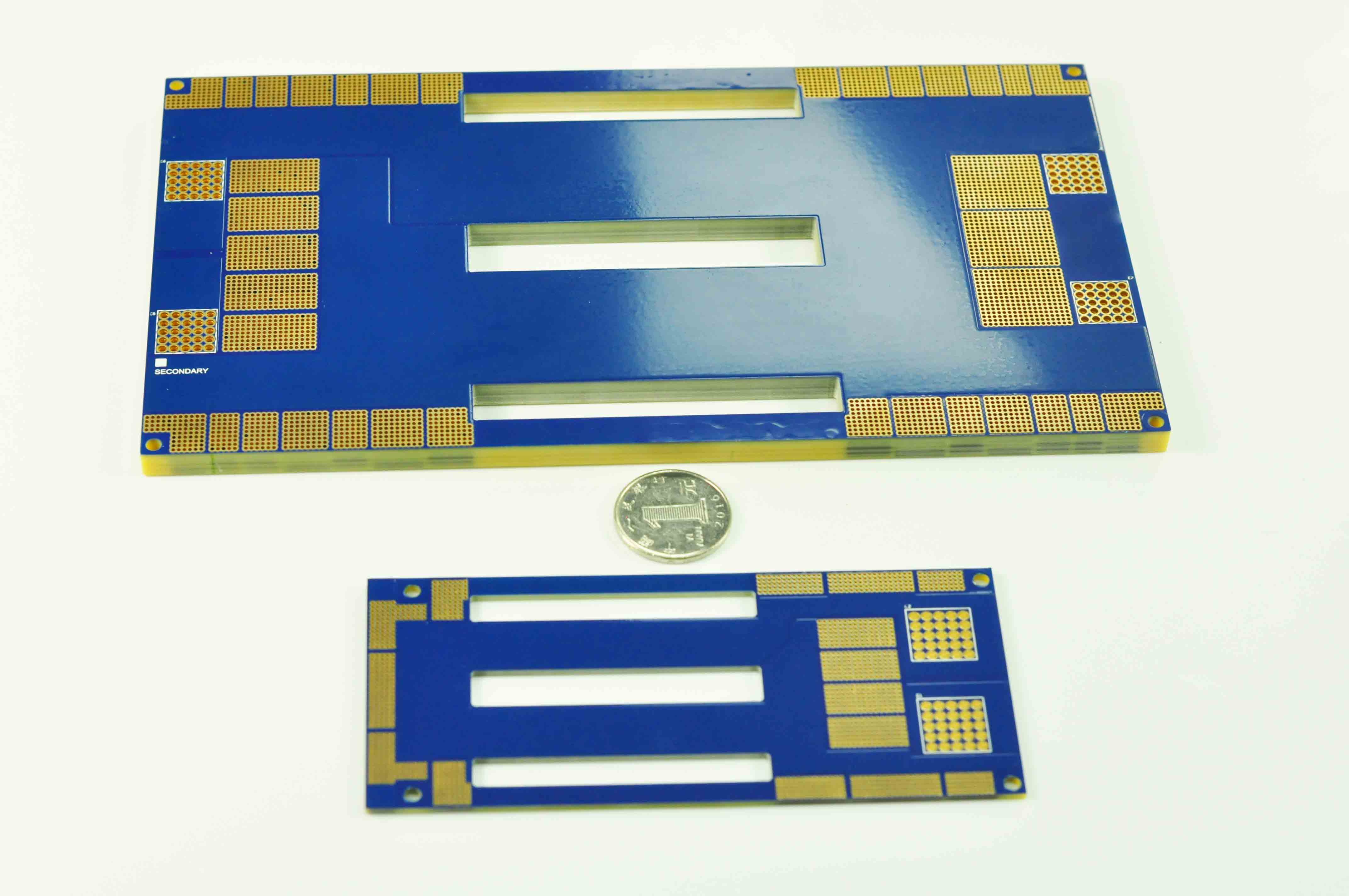
All of us know the printed circuit board, but do you know what is the heavy copper PCB? Best Tech is a very experienced heavy copper PCB fabricator since year 2006. Heavy Copper PCB is a type of printed circuit board that features with thicker copper layers than standard FR4 PCBs. While conventional PCBs typically have copper thicknesses ranging from 1 to 3 ounces (per square foot), heavy copper PCBs have copper thicknesses exceeding 3 ounces and can go up to 20 or more ounces. These copper layers are typically found in the inner and outer layers of the PCB, heavy copper providing enhanced current-carrying capacity and improved heat dissipation capabilities.

The increased copper thickness in heavy copper PCBs allows them to handle higher currents without experiencing excessive heat buildup or voltage drops. This makes them well-suited for applications that require high power handling, such as industrial power supplies, power converters, motor drives, and automotive electronics. Heavy copper PCBs are designed to withstand harsh operating conditions and provide robust performance and reliability.

Today, we would like to talk about the heavy copper PCB used in Industrial Power Supply. In this blog post, we will explore the realm of Industrial Power Supply, delving into the design considerations, material selection, production challenges, exceptional heat dissipation, and unrivaled conductivity of Heavy Copper PCBs. Join us on this enthralling journey as we uncover the secrets behind their application in Industrial Power Supply scenarios, including the testing of inductance, capacitance, and resistance. Get ready to witness the power of Heavy Copper PCBs in the realm of Industrial Power Supply!

Firstly, before you are moving start for the design, it need to get to understand the Design guideline rules of heavy copper PCB.

From the guidelines of heavy copper PCB, it could get to know it encompass considerations such as trace width, trace spacing, and thermal relief patterns. The increased copper thickness necessitates wider traces to accommodate higher currents, while proper spacing is crucial to avoid thermal hotspots and ensure reliable operation. Additionally, selecting suitable materials with excellent mechanical strength and thermal properties is vital to ensure the robustness and longevity of Heavy Copper PCBs. Hope this will bring some ideas to you during your design.

Secondly, as a heavy cooper PCB manufacturing vendor, Best Tech would like to advise the Production Challenges for the heavy copper PCB.

During producing Heavy Copper PCBs presents manufacturers with a set of intricate challenges. Achieving uniform copper thickness across the board’s surface demands advanced plating techniques and precise control over process parameters. Careful attention must be given to the etching process to prevent over-etching, which can compromise the integrity of the copper layers. Moreover, the additional weight of copper requires a sturdy substrate to support the board’s structure. Manufacturers must navigate these challenges with expertise and precision to deliver high-quality Heavy Copper PCBs.

You may have a question in mind, why we need to use the heavy copper PCB for the Industrial Power Supply, because the heavy copper PCB have Exceptional Heat Dissipation and Conductivity: One of the standout features of Heavy Copper PCBs is their unrivaled heat dissipation capabilities. The increased copper thickness acts as a robust conductor, efficiently channeling heat away from power components. This exceptional heat dissipation prevents thermal stress and ensures the longevity and reliability of Industrial Power Supply systems. Additionally, the high conductivity of Heavy Copper PCBs enables efficient power transmission, reducing losses and improving overall system efficiency.

Furthermore, Heavy Copper PCBs undergo rigorous testing to ensure optimal performance in Industrial Power Supply applications. Inductance testing verifies the effectiveness of copper layers in reducing magnetic interference. Capacitance testing evaluates the ability of the PCB to store electrical energy, while resistance testing determines the conductivity and resistance of copper traces. These tests play a crucial role in validating the quality and performance of Heavy Copper PCBs in demanding power supply scenarios.

Heavy Copper PCBs find widespread applications in the field of Industrial Power Supply, particularly in the production of robust and efficient power control products. They are integral components in industrial power converters, motor drives, uninterruptible power supplies (UPS), and various automation systems. The exceptional heat dissipation and high current-carrying capacity of Heavy Copper PCBs make them ideal for handling the power demands of these applications, ensuring reliable and efficient power delivery.

Finally, in the world of Industrial Power Supply, Heavy Copper PCBs emerge as true powerhouses, combining meticulous design, advanced manufacturing processes, and exceptional heat dissipation capabilities. By adhering to design guidelines, overcoming production challenges, and conducting thorough testing, Heavy Copper PCBs prove their mettle in demanding power supply scenarios. As they continue to evolve, these powerhouses will shape the future of Industrial Power Supply, empowering systems with reliability, efficiency, and unrivaled performance. Prepare to witness the electrifying impact of Heavy Copper PCBs in the realm of Industrial Power Supply!

If you have more question heavy copper PCB for Industrial Power Supply, warmly welcomed to contact Best Tech for more get more information of heavy copper PCB which used in Industrial Power Supply. You can visit www.bestpcbs.com to know more about us.

You may also like