PCB manufacturing PCB manufacturing
Home > Blog

Reflow Profiling

PCB Thermocouple Placement for Reflow Profiling and Temperature Measurement
Thursday, September 17th, 2026

A PCB thermocouple records how hot a specific point on an assembly gets during reflow and how long it stays there. Place sensors where a joint may heat too slowly or a component may get too hot, then secure them so the readings reflect the assembly rather than the attachment. The profile must show that critical joints receive enough heat without exceeding the monitored component limits.

PCB Thermocouple, instrumented circuit board connected to a reflow profiling data logger

What Is a PCB Thermocouple and What Does It Measure During Reflow?

A PCB thermocouple is a welded junction of two dissimilar conductors fixed to a defined point on a populated circuit board. It records local temperature versus time at the junction; it does not measure the oven setpoint or provide one temperature for the whole assembly.

The contact point determines what the curve represents. A junction attached to a lead heel or pad can track solder-joint heating. A package-top junction checks component-body temperature. A sensor suspended above the board measures local air and cannot prove that a hidden termination reached the required soldering window.

Keep the conductors insulated up to the welded bead. If the bare wires touch before that bead, the contact can become a second measuring junction and shift the apparent location. Record the component reference, exact contact point, attachment method, channel number, and measurement purpose before the run.

Why Does PCB Thermocouple Placement Affect Temperature Measurement Accuracy?

A temperature trace is useful only when its sensing point represents the joint or component being checked. Joints connected to large copper areas may heat slowly, while exposed edge components may reach a higher peak. A well-attached sensor at a convenient but unrelated spot can still give the wrong basis for setting the oven recipe.

  • Thermal mass: Large connectors, shields, transformers, and dense component groups usually heat more slowly than small exposed devices. Place the junction on the joint or body that could limit the process.
  • Copper connection: A pad tied to a plane or heavy copper can lag behind a nearby isolated pad. Check the actual copper path instead of assuming adjacent joints behave alike.
  • Airflow exposure: Board edges, leading corners, and unshielded parts may heat faster than central or shadowed areas. Add separate points when orientation or panel position changes airflow.
  • Attachment mass: Excess solder or thick adhesive slows sensor response. The bead should touch the target directly with only enough material to hold it.
  • Measurement target: Package temperature and joint temperature are different acceptance checks. Label every channel by both location and purpose.

Where Should Thermocouples Be Placed on a PCB for Reflow Profiling?

Place thermocouples at the points most likely to narrow the reflow process window. The minimum plan covers a suspected cold joint, a suspected hot point, and any component or termination with a critical temperature requirement. Add panel positions only when copper distribution, component loading, or airflow can make them thermally different.
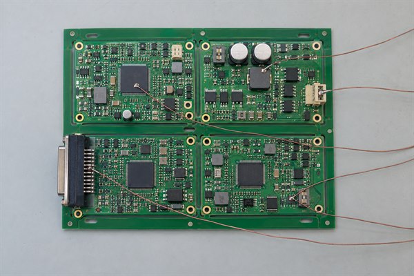
Multiple fine-wire thermocouples attached to different thermal-risk locations on a populated PCB panel

Choose candidate points from the assembly drawing, BOM, copper layout, panel orientation, and component limits. A cold-joint point matters when insufficient heat there could prevent an otherwise acceptable recipe; it need not be the lowest reading anywhere on the board.

Profile Point Recommended Location Verification Target
Cold joint Critical pad tied to a large plane, heavy copper, or high-mass component Peak and time above liquidus at the slowest relevant joint
Hot point Small exposed component or joint near a board edge Maximum temperature and available upper margin
Critical joint Exact lead heel, pad, or accessible hidden termination tied to reliability risk Solder-joint thermal exposure at the required connection
Sensitive part Specified package-body or lead location Component temperature limit
Panel variation Representative edge, center, leading, and trailing assemblies Temperature spread caused by panel position

Mark each location on an assembly drawing or photograph, including the exact contact point and why it is monitored. “TC4—U12 corner ball—cold-joint check” is more useful than “TC4” alone.

How Many Thermocouples Should Be Used for PCB Reflow Profiling?

Use enough channels to cover the thermal risks that could change the oven recipe. Roughly three to five points may cover a small, uniform assembly; a large panel or mixed-mass board may need six to twelve or more. The number depends on the actual risks, not a fixed profiling rule.

  • Cover both extremes: Include at least one predicted cold location and one predicted hot or temperature-sensitive location.
  • Add critical interfaces: Give separate channels to hidden terminations, high-reliability joints, or body limits that cannot be represented by the existing points.
  • Sample real panel differences: Add edge, center, leading, or trailing positions only where layout and airflow make a different result plausible.
  • Avoid measurement disturbance: Do not fill spare channels without a purpose. Dense wire bundles can alter airflow, pull on junctions, or interfere with the conveyor.

If the profiler lacks enough inputs, divide the plan into controlled repeat runs. Keep the oven recipe, conveyor direction, assembly state, and at least one reference channel unchanged so the groups can be compared.

Which Thermocouple Type and Wire Size Are Suitable for PCB Temperature Measurement?

Fine-wire Type K thermocouples are commonly suitable for electronics reflow profiling when they match the profiler input, connector polarity, temperature range, and insulation rating. A smaller conductor responds faster and disturbs a small joint less; a larger conductor is more durable but conducts more heat and needs more routing space.

About 0.2 mm wire is a practical choice for accessible joints; about 0.1 mm may help reach a BGA or fine-pitch target. These are examples, not required sizes. Choose a wire fine enough for the contact point but robust enough to stay attached through the planned runs.

  • Profiler match: Confirm thermocouple type, connector type, polarity, and channel configuration before installation.
  • Target access: Use finer wire when the junction must reach a hidden or closely spaced termination without bridging nearby conductors.
  • Thermal response: Keep the welded bead and exposed conductor length small enough to follow the target rather than surrounding air.
  • Mechanical life: Use insulation and strain relief that can survive the full oven cycle without softening, shorting, or contaminating the assembly.

How Should Thermocouples Be Attached and Routed on a PCB?

Fix the welded junction in direct, low-mass contact with the target and strain-relieve the wire before routing it toward the rear of conveyor travel. High-temperature solder is effective on accessible metal points; qualified high-temperature adhesive may suit package surfaces. Tape is better used for lead restraint than as the only precision contact at a solder joint.
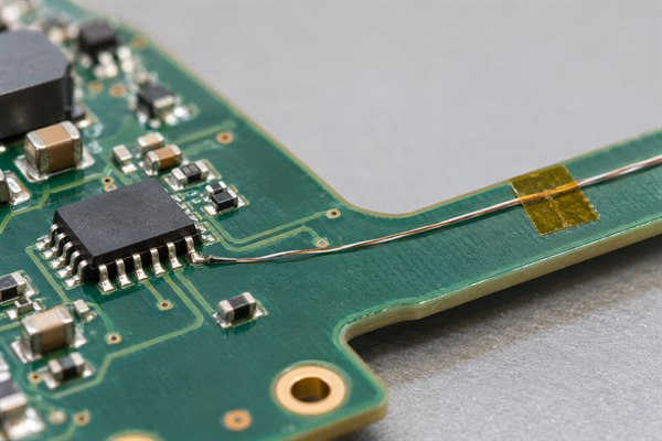
Fine-wire thermocouple junction attached to a component lead with flat routing and tape strain relief
  1. Prepare the point: Clean and identify the exact pad, lead, joint, or package location. Confirm that the selected point matches the channel plan.
  2. Attach the bead: Use the smallest secure amount of high-temperature solder or approved adhesive. Under magnification, the junction should touch the target directly.
  3. Add strain relief: Restrain the lead a short distance from the bead. A gentle pull on the cable should not move the sensing point.
  4. Route the wire: Keep it close to the board, away from moving hardware and hot oven surfaces, and clear of the local airflow being measured.
  5. Check the channel: Verify continuity, polarity, channel label, and room-temperature response before the board enters the oven.

When high-temperature solder is used, the attachment alloy must remain solid during the measured cycle. Remove incompatible low-melting solder from a sacrificial profile point where necessary, and avoid a large solder fillet that would add thermal mass.

What Thermocouple Placement Challenges Occur with BGAs, QFNs, Large Components, PCB Panels?

Hidden joints, component bodies, and panel positions cannot all be judged from the same sensing point. When a joint cannot be instrumented directly, a nearby reading can help investigate heating, but it must not be reported as that joint’s temperature.

  • BGA: A package-top sensor measures body temperature. It does not prove solder-ball temperature. Direct joint measurement may require a sacrificial assembly and controlled underside access to a selected ball.
  • QFN or LGA: An exposed perimeter pad may not represent the center thermal pad. Use underside access or a purpose-built profile sample when center-joint behavior controls the decision.
  • Large component: Connectors, transformers, and shields can create a slow joint while the component body has a separate maximum-temperature limit. Monitor both when either can restrict the recipe.
  • PCB panel: Measure representative edge, center, leading, and trailing positions when panel layout or airflow can create a meaningful thermal gradient. Compare those positions before assuming that one assembly’s profile represents every board in the panel.
  • Dense assembly: If simultaneous wiring would disturb airflow or prevent safe conveyor travel, use controlled repeat runs with a stable reference channel.

How Do You Evaluate Temperature Data from PCB Thermocouples During Reflow?

Compare each curve with the requirement for the point it actually measures. Joint traces use the selected solder-paste and alloy limits; component-body traces use the applicable component limit. Oven zone settings and conveyor speed are inputs, while the thermocouple curves show the temperature experienced by the assembly.

  • Ramp rate: Calculate the heating slope where required and check whether fast and slow locations remain within the applicable process limits.
  • Soak: Check the time and temperature range specified for the selected paste process, rather than applying a generic soak target.
  • Time above liquidus: For each critical joint, measure the interval between the trace rising above and falling below the alloy’s liquidus temperature. Compare that interval with the selected paste’s process window.
  • Peak temperature: Compare joint and package peaks with their own limits; one peak limit should not be applied to every channel.
  • Cooling rate: Review the cooling slope when it is part of the product or paste requirement.
  • Temperature spread: Compare decision-relevant channels in the same run. A cold joint and a hot package must both meet their respective limits; a small spread by itself does not prove either result.

Accept a recipe only when every critical joint and monitored package meets its own limit in the same run. If improving a cold joint pushes a component past its limit, change one controlled input—such as zone temperature, conveyor speed, or orientation—and profile again. Compare the new traces against the same channel locations and requirements.

What Causes Inaccurate PCB Thermocouple Temperature Measurements?

The most common causes are a moved junction, excessive attachment mass, damaged wiring, incorrect profiler setup, or a sensor placed on the wrong thermal object. Diagnose the trace together with the physical installation and channel record.

Trace Pattern Likely Cause Corrective Check
Abrupt step or drift Junction moved or lifted Inspect the bead and strain relief; repair and repeat
Intermittent spikes Loose connector, broken wire, or unintended conductor contact Check continuity, insulation, polarity, and connector seating
Unusually slow response Excess solder, thick adhesive, or heavy wire Compare with a lower-mass attachment at the same target
Smooth curve but poor soldering result Wrong target or surface proxy used as joint data Match the channel record and photographs to the physical contact point
Poor run-to-run agreement Attachment damage or changed loading, orientation, or board condition Repeat under controlled conditions with one stable reference channel
All channels shifted Wrong thermocouple type, logger setup, or cold-junction compensation Verify the profiler configuration and perform a known-temperature check

A smooth trace does not establish where the bead was attached. Reject a channel if its contact point cannot be confirmed after reflow, and repeat the measurement with a documented attachment.

How Can You Verify That PCB Thermocouple Measurements Are Reliable?

Check the sensor before and after reflow, confirm the profiler settings, and repeat the critical measurements. Compare runs only when the board revision, channel map, and oven recipe match.

  1. Inspect the installation: Verify bead contact, attachment size, insulation, strain relief, polarity, and connector seating. Save close-up photographs of every point.
  2. Test channel identity: At a stable room temperature, apply a controlled touch or heat stimulus to each junction. Only the expected channel should respond.
  3. Confirm the profiler: Check thermocouple type, sample interval, trigger, channel labels, and calibration status. Save the configuration with the run.
  4. Profile the real thermal load: Use the intended panel, component population, carrier, conveyor direction, and loading condition. Record any deviation.
  5. Inspect after reflow: Reject data from a junction that moved, lifted, shorted, or was damaged. Match accepted traces to the saved photographs.
  6. Repeat the run: Hold the recipe and assembly conditions constant, then compare peak, time above liquidus, ramp, and spread on the critical channels.

Reprofile when a change can alter heat transfer or the allowable window. Typical triggers include a new paste, a package or component-mass change, revised copper or stackup, a new panel layout, a different carrier, major oven maintenance, or transfer to another production line.

FAQs About PCB Thermocouple Placement and Reflow Profiling

Q1: Can a bare PCB be used for reflow profiling?

A1: A bare board cannot establish the final assembly profile. Components, solder deposits, shields, and connectors change thermal mass and airflow. Use a populated production-representative assembly or a documented equivalent profile vehicle for recipe approval.

Q2: Does changing solder paste require a new reflow profile?

A2: Reprofile if the required thermal window changes. Compare liquidus temperature, time above liquidus, soak guidance, peak range, and cooling requirements before using the existing recipe.

Q3: When does a design or BOM change require reprofiling?

A3: Reprofile when the change can affect heat transfer or a temperature limit. Large copper changes, board-thickness changes, added shields, heavier connectors, alternate packages, and revised sensitive components are common triggers.

Q4: Can a thermal camera replace attached thermocouples?

A4: A thermal camera can locate surface hot and cold regions, but it cannot automatically replace contact profiling. Emissivity, viewing angle, and line of sight limit the result, especially at hidden BGA and QFN joints.

Q5: Can the same profiling board be reused indefinitely?

A5: No. Set an inspection and retirement rule. Repeated heat cycles and handling can age the assembly, loosen attachments, and damage fine wires. Retire or rebuild the board when it no longer represents production.

Q6: What should be saved with a PCB reflow profile?

A6: Save enough data to reproduce the installation and oven run. Keep the raw traces, calculated metrics, channel map, attachment photographs, product and BOM revisions, paste identity, panel orientation, oven recipe, profiler settings, and calibration status.

For a PCBA quotation with reflow-profile or reporting requirements, send Gerber or ODB++, a BOM with exact part numbers, assembly and panel drawings, solder-paste requirements, quantity, target delivery date, and required profile or inspection records to sales@bestpcbs.com. Include any joints or component limits that need separate temperature measurements so the quotation can account for them.

You may also like

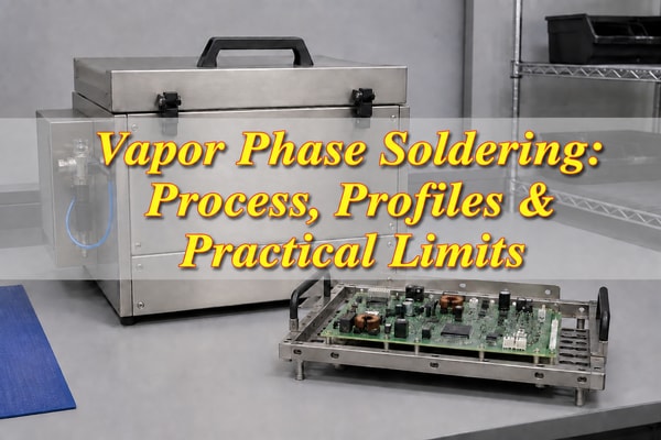
Vapor Phase Soldering: Process, Profiles & Practical Limits
Friday, September 4th, 2026

Vapor phase soldering heats a PCB assembly by condensing hot vapor on its cooler surfaces. The released heat melts the solder alloy in the paste and forms the joints. Also known as condensation soldering or vapor phase reflow, this method can help when large, slow-heating parts share a board with small, temperature-sensitive components.

Its main appeal is controlled heat transfer across that mixed assembly. The fluid limits the heating temperature; it does not guarantee a good solder joint. Fluid selection, the measured board profile and inspection results still determine whether the process suits the PCB.

Vapor phase soldering, illustrative laboratory reflow equipment and a populated PCB carrier with the article title

How Does Vapor Phase Soldering Work?

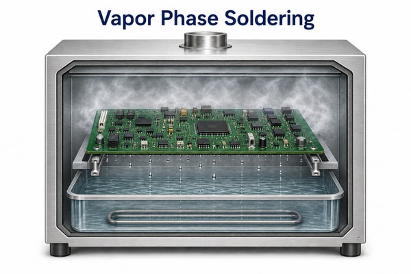
When vapor condenses on the PCB, it releases latent heat directly to the board and components. The vapor comes from a purpose-made heat-transfer fluid, not water. That fluid carries heat; the solder paste supplies the metal that joins each component termination to its pad.

In a conventional saturated-vapor machine, heaters boil the fluid beneath a controlled vapor zone. A carrier holds the assembly in that zone while condensate forms on its surfaces and drains back into the reservoir. Some machines instead meter fluid into a process chamber, so the loading and vapor-delivery sequence depends on the equipment.

Condensation heating falls as the board approaches the vapor temperature. At a given pressure, the fluid’s boiling point sets the temperature ceiling for this heating method. A component rated below that temperature can still be damaged, while a heavy copper area may take longer to reach soldering temperature.

Vapor phase soldering, conceptual chamber cutaway with a populated PCB on a carrier above heat-transfer fluid and condensate returning to the reservoir

What Are the Steps in Vapor Phase Soldering?

After solder paste printing and component placement, the board moves through loading, preheating, reflow and cooling. Vacuum may be added during the molten-solder stage when the process calls for it.

  • Prepare the board before heating. Verify the board revision, paste, component orientation and moisture-handling requirements. Inspect the deposits and placement: reflow cannot repair missing paste or a wrongly fitted part.
  • Load the board on a stable carrier. Allow for its outline, weight and underside components. Supports must hold the assembly through heating and cooling without pressing on parts.
  • Preheat at the required rate. Adjust preheat or vapor delivery to suit the paste and component limits. The measured ramp and soak should allow flux activation and volatile release without excessive thermal stress.
  • Bring the critical joints through reflow. Hold them within the required temperature and time limits. Check both the slowest-heating joints and the most heat-sensitive components.
  • Apply vacuum only when the process includes it. Coordinate pressure and timing with the molten-solder interval. Save the pressure cycle alongside the temperature trace so the result can be repeated.
  • Cool before unloading and inspection. Recover the working fluid and keep the board supported as the joints solidify. Inspect accessible and hidden joints using the specified methods, then complete the electrical tests.

Vapor phase reflow does not require vacuum. A non-vacuum machine can produce acceptable joints when the profile, materials and assembly meet the product’s requirements.

What Fluid Is Used in Vapor Phase Soldering?

Common vapor phase soldering fluids are perfluoropolyethers, or PFPEs. The selected grade sets the nominal vapor temperature at the operating pressure. Grades with similar names or boiling points are not necessarily interchangeable.

Galden LS/HS grades, for example, are designed for vapor phase soldering; general-purpose HT grades have different distillation-range and vapor-temperature controls. Choose a soldering fluid that matches the machine specification, solder paste and component limits.

A 230°C fluid will not become a 245°C heat source because the board stays in longer. In saturated vapor at the specified pressure, extra dwell gives colder joints more time to approach the vapor temperature. If the paste needs a peak the fluid cannot provide, change the fluid, paste or process.

Include fluid recovery, maintenance and consumption in the operating-cost estimate. Follow the current technical and safety data for machine compatibility, hot-fluid handling and disposal; chemical inertness does not remove those precautions.

How Do You Measure a Vapor Phase Soldering Profile?

Measure temperatures on the assembly, rather than judging the profile from the vapor reading alone. A vapor phase soldering temperature profile needs to show how the critical joints and components heat, dwell and cool.

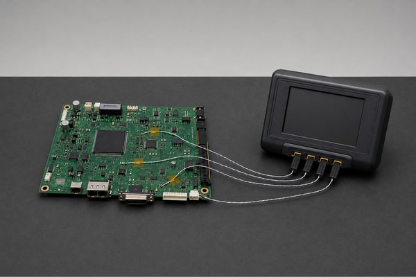
Place thermocouples at a large thermal pad or copper-rich area, a small fast-heating location and a temperature-sensitive component. Identify whether each sensor measures a joint or a package body—their limits may differ. Use the intended carrier and a representative production load.

Vapor phase soldering, illustrative PCB with thermocouple leads connected to a logger with a blank display
  • Heating rate and soak: look for uneven heating. If small parts heat much faster than a large pad, adjust preheat or vapor delivery and measure again. Keep the ramp and dwell within the paste and component limits.
  • Peak temperature: both hot and cold locations must pass. The coldest critical joint must reach the paste’s process window while the hottest monitored component stays within its limit.
  • Time above liquidus: measure each critical joint. Too little time above the alloy’s liquidus temperature can leave incomplete wetting. Extending that interval also affects flux behavior and intermetallic growth, so use the paste’s specified window.
  • Cooling: keep recording until the joints solidify. Check the specified cooling limits and keep the assembly supported. Stopping the trace at peak temperature leaves this part of the profile unverified.

There is no universal temperature recipe for VPS. Indium Corporation gives a preferred peak of 230–240°C for the SAC pastes in its vapor-phase application note, and 30–90 seconds above liquidus for the Pb-free no-clean pastes it describes. Those ranges apply to the materials discussed. Set your trial from the current paste data sheet and the most restrictive component limits.

What Causes Common Vapor Phase Soldering Defects?

Trace defects through paste printing, placement and the measured profile before changing the heat settings. Note which parts fail and when the problem first appeared. A lifted resistor and a solder bridge may need very different corrections.

  • Tombstoning: compare the two ends of the lifted part. Unequal wetting forces can pull a small resistor or capacitor upright. Check paste volume, placement and whether the copper connections make one pad heat sooner. If printing and placement are balanced, try a gentler ramp within the paste’s limits and recount defects at those locations.
  • Component shift: find out when the part moves. Check its position and paste alignment before reflow. Movement that begins only with vacuum calls for a pressure-trace review. Trial a less abrupt evacuation cycle without losing the required soldering conditions, then inspect for beads and bridges as well as alignment.
  • Excessive voiding: check the joint before increasing vacuum. Poor wetting or insufficient solder can leave unfilled areas as well as trapped gas. Compare X-ray patterns, deposit volume, paste condition and the joint profile. Once those are stable, assess a controlled vacuum trial using the same imaging method and acceptance limit.
  • Solder balls or spatter: review paste handling and the heating ramp. Rapid heating can contribute to volatile release and spatter; poor coalescence can leave separate particles. Check deposit shape and trial the recommended preheat conditions. If the defect begins with vacuum, review the evacuation rate too.
  • Incomplete wetting: separate a heat problem from a surface problem. Verify joint peak temperature and time above liquidus. If both meet the material requirements, investigate pad and termination solderability, contamination, paste condition and flux performance before adding heat.
  • Bridging: correct excess paste or placement offset first. Look for paste between adjacent pads and misaligned parts. If both printing and placement are sound, investigate slump or movement during heating and vacuum. Change one suspected cause at a time so the next build shows whether it helped.

Compare defect counts across similar batches, not just one clean board. Keep an unchanged reference build where practical and inspect the same locations after each adjustment. Repeat at representative production loads before treating the correction as stable.

How Does Vacuum Vapor Phase Soldering Reduce Voids?

Vacuum lowers the pressure around molten solder, helping trapped gas expand and escape before the joint solidifies. Paste control, pad design and wetting remain important because vacuum cannot correct every cause of an unfilled joint.

The pressure level, evacuation rate, dwell and solder temperature work together. An abrupt pressure change can disturb the solder or shift components. More aggressive vacuum is not automatically a better process.

Where practical, compare the existing process with VPS both with and without vacuum. Keep the board, paste, stencil and inspection method unchanged. Measure void area and location, then inspect for displaced parts, beads, bridges and insufficient solder.

Accept a low-void result only against a defined measurement method and limit. Agree which joint area is measured and how the percentage is calculated. Use suitable X-ray inspection of hidden solder joints to assess the trial boards; neither a machine’s advertised figure nor an X-ray result alone establishes lifetime reliability.

Vapor Phase vs Convection Reflow: What Is the Difference?

Vapor phase uses condensation to deliver heat; convection reflow uses circulating hot gas. Both reflow solder, so VPS is a type of reflow soldering rather than an alternative to reflow itself.

Process factor Vapor phase Convection reflow
Heat delivery Vapor condenses on cooler surfaces and releases latent heat. Circulating heated air or nitrogen transfers heat to the assembly.
Profile control Fluid grade, preheat, vapor delivery, exposure and pressure depend on the machine. Zone temperatures, gas flow and transport speed shape the profile.
Mixed thermal mass Strong condensation heat transfer can help heat large and small features within one process window. Zone and transport settings must bring cold joints into range without exceeding hot-part limits.
Process atmosphere The working-fluid vapor provides an inert environment in the soldering zone. Air and nitrogen configurations are available.
Void reduction A vacuum option can remove gas while solder is molten. Selected systems also include vacuum; it is not exclusive to vapor phase.

Compare joint quality, temperature spread and accepted boards per hour on the same assembly. Keep the board revision, paste, placement quality and inspection criteria consistent. Batch and inline handling are separate choices; commercial VPS equipment is available in both forms.

When Should You Use Vapor Phase Soldering?

Consider VPS when getting a cold joint hot enough pushes another component too close to its temperature limit. That conflict in the measured profile gives a clearer reason to try the process than board size, package name or order volume alone.

  • Large boards with uneven heating. Power planes, thick copper and large connectors heat differently from small chip components. A useful VPS trial should show a smaller temperature spread at the critical locations while all monitored parts stay within their limits.
  • BGA packages with difficult thermal profiles. Vapor phase soldering for BGA assemblies can help heat a large package and its underlying joints. Pad design, paste deposits, warpage and moisture still affect the result, so combine board profiling with hidden-joint inspection.
  • Power devices where voids affect the thermal path. A vacuum-capable process may help large soldered thermal pads. Define the X-ray method and joint-specific limit before the trial; void location and the largest void can matter alongside total void area.

Keep convection if it already delivers acceptable joints, a repeatable profile and the required output at a suitable cost. Rule out printing, placement and material problems before changing the heating method. If voiding is the only remaining issue, compare vacuum options in both types of equipment.

A difficult low-volume board may justify VPS for thermal control alone. In repeat production, weigh any quality improvement against loading, cooling, inspection and fluid costs. The trial needs to show an improvement worth the added cost or cycle time.

What Are the Disadvantages of Vapor Phase Soldering?

The main drawbacks are fluid costs, equipment costs, setup work and cycle time that varies with the load. Efficient heat transfer is useful only when its rate stays within the assembly’s limits.

  • The board can heat too quickly. Even a fluid with the right boiling point needs controlled preheating and exposure. Test the ramp and dwell at the intended load, where fast-heating parts may approach their limits sooner.
  • The fluid temperature may not suit every material. It may be too low for the paste or too high for a component. Resolve conflicting limits before production; a longer dwell cannot fix that mismatch.
  • Fluid recovery adds running costs. The initial charge, carry-out losses, filtration and maintenance all count. Compare consumption for the proposed load and handling method as well as the fluid purchase price.
  • Cooling and handling can limit output. Include loading, preheat, vacuum, cooling and unloading in the cycle estimate. A short reflow step alone does not tell you how many boards the machine can deliver.

Normal moisture-control requirements still apply. Staying below the fluid’s boiling point does not prevent damage from trapped moisture, excessive exposure or an unsuitable material.

How Do You Verify Vapor Phase Soldering Quality?

A good temperature trace must be backed by acceptable joints and the required test results. Set the acceptance limits before the trial, then keep the following information together so the approved build can be repeated.

  • Start with a defined board and material set. Keep the PCB and assembly revisions, construction, component list, paste product and lot, solder alloy and fluid grade together with their temperature, moisture and joint-acceptance limits. Resolve any conflict before running the trial.
  • Make the loading arrangement repeatable. Note the machine, carrier, supports, board orientation and batch size. Mark sensor positions on a drawing or photograph, including whether each measures a joint or package body. Later profiles can then be compared on the same basis.
  • Save the measured curves and their recipe. For each critical location, retain the ramp, peak, time above liquidus and cooling trace against its limits. A vacuum build also needs pressure, evacuation rate, dwell and timing relative to the molten-solder interval.
  • Keep inspection results tied to the boards inspected. Record the sample count and reference designators, visual or automated optical inspection findings, and required X-ray views. Void results need the measured area, calculation method and limit. Include bridges and shifted parts, even if voiding improves.
  • Test the assemblies and repeat the build. Retain the test procedure, limits and results for each board or batch. Repeat at representative loads using a sample plan matched to product risk. Functional testing alone does not qualify every joint; reliability or destructive tests may also be needed.
  • Define what requires another trial. Name the approver and any unresolved deviations. Changes to paste, fluid, major components, copper construction, loading or recipe may require a new profile or qualification review. Keep the approved settings and supporting results accessible to production.

A trial fails if fixing the cold joint overheats another component. Adjust the available controls, measure both locations again and repeat the affected inspection and tests. The accepted process must suit the whole assembly.

How Do You Choose a Vapor Phase Soldering Machine?

Choose a machine that fits the populated board, can achieve its profile and meets the required output. Compare price only after the quotations include the same necessary functions.

A compact batch vapor phase reflow oven may suit laboratory work or short runs, while an inline system may fit a continuous line. In either case, use the actual board and loading arrangement to judge handling, process control and cycle time.

  • Usable board space and support. Supply panel dimensions, assembly weight, component heights on both sides and support restrictions. The usable carrier area and clearances matter more than the chamber’s outside dimensions.
  • Temperature and vacuum controls. Compare supported fluid grades, heating adjustments, measurement features and pressure-cycle control. For a narrow process window, ask for a trial on a representative board.
  • Fit with the production line. Check loading, cooling, line interfaces, recipe access and process records. Estimate output from the full cycle and planned utilization.
  • Installed and operating costs. Include required options, fluid charge and losses, filtration, utilities, maintenance, labor, qualification and inspection. This makes the machine-price comparison meaningful.

When outsourcing PCB assembly, confirm access to VPS equipment before specifying the process in an order. Ask where the work will be done and which qualification records are included; general SMT capability does not establish VPS availability.

FAQ About Vapor Phase Soldering

Q1: Are vapor phase soldering and vapour phase soldering different?

A1: They are spelling variants. “Vapor” is American English and “vapour” is British English. VPS, vapor phase reflow and condensation soldering commonly refer to the same heating principle. Individual machines may use different vapor-delivery and profile-control methods.

Q2: Does the process need nitrogen?

A2: The basic condensation process does not need a separate nitrogen supply. The working vapor can provide the inert soldering atmosphere. Some machines still use nitrogen for chamber or cooling functions, so confirm the utilities for the model and configuration being considered.

Q3: Can double-sided PCBs use vapor phase reflow?

A3: Yes, with a suitable assembly sequence and carrier. Allow clearance for underside components and consider how they will stay in place during the second heating cycle. Heavy parts may need another sequence or retention method. Trial the populated board on its intended carrier and account for cumulative thermal exposure.

Q4: Does the working fluid remove the need to clean flux residue?

A4: No. Recovering the working fluid does not remove the need to assess flux residue. Cleaning depends on paste chemistry, residue behavior and later operations such as conformal coating. Check the assembled product against its cleanliness and material-compatibility requirements.

Q5: Can vapor phase equipment be used for rework?

A5: Some systems support desoldering and repair with suitable tools and a qualified process. Other components and underside joints also experience the additional thermal cycle. Check their limits and moisture history, then inspect and retest the repaired circuit. Identify the fault before deciding to reflow the board.

Conclusion

Choose vapor phase soldering when trials show a useful improvement in thermal control or joint quality at an acceptable production cost. Match the fluid to the paste and component limits, measure the board profile and evaluate vacuum if voiding remains a problem. A working convection process may already be the better fit.

For a free DFM review with BestPCBS, send your Gerber or ODB++ files, BOM with exact part numbers and allowed alternatives, assembly drawing, quantity, target delivery and inspection requirements to sales@bestpcbs.com.

Include the solder alloy, temperature-sensitive parts and any voiding limit. If VPS is required, ask the team to confirm the process and availability for your project before quotation.

You may also like