PCB manufacturing PCB manufacturing
Home > Blog

EBest Circuit: Your One-Stop PCB & PCBA Manufacturing Partner

August 24th, 2026

EBest Circuit is a one-stop PCB and PCBA manufacturing partner founded in 2006. We support bare PCB fabrication, component sourcing, SMT and through-hole assembly, testing, prototype builds, and volume production for global electronics projects.

If you are evaluating a PCB supplier for a new project, send us your Gerber files, BOM, stack-up, quantity, and testing requirements. Our engineering team can review the manufacturing package before quotation and help identify process risks early.

Item EBest Circuit Support
Core services PCB fabrication, component sourcing, PCBA assembly, testing, box-build support
Project stage Prototype, small-volume build, and volume production
Manufacturing support Shenzhen, China and Vietnam manufacturing support
Technical review DFM, stack-up, material, copper weight, impedance, assembly and test review
Typical files for review Gerber, drill, stack-up, BOM, pick-and-place, drawings and test requirements
EBest Circuit one-stop PCB and PCBA manufacturing partner hero image

Who Is EBest Circuit?

EBest Circuit is a PCB and PCBA manufacturing partner for electronics teams that need more than a bare-board supplier. We help customers move from early design review to PCB fabrication, component sourcing, assembly, inspection, and production planning.

Our work covers conventional rigid PCB projects as well as more specialized requirements such as HDI, RF/high-frequency materials, heavy copper, metal-core PCB, ceramic PCB, flexible PCB, rigid-flex PCB, and turnkey PCBA. For each project, we review the actual files instead of treating a single capability number as a universal answer.

What Can We Build?

We support both standard PCB technologies and project-specific builds that require engineering review. The best starting point is a complete manufacturing package, because layer count, material, copper weight, hole structure, board size, surface finish, assembly requirements, and testing all affect feasibility.

Product or Service Typical Support
Rigid PCB Single-sided, double-sided and multilayer rigid PCB fabrication
HDI PCB Fine features, laser blind/buried vias and high-density interconnect structures
RF / High-Frequency PCB Rogers, Taconic, PTFE, Isola, Nelco and other specified laminates
Heavy Copper PCB High-current and mixed-copper designs reviewed by stack-up and copper distribution
Metal-Core PCB Aluminum, copper and stainless-steel substrate options
Ceramic PCB Thin Film, DBC/DCB, DPC and AMB ceramic substrate technologies
Flexible PCB Single-, double- and multilayer FPC through our flexible PCB support path
Rigid-Flex PCB Combined rigid and flexible structures for compact electronic assemblies
PCB Assembly SMT, THT/DIP, mixed assembly, component sourcing and agreed testing
Box-Build Support PCB with cable, wire, enclosure or project-specific assembly requirements

For flexible PCB and rigid-flex projects, customers can also review our dedicated flexible PCB manufacturing resources at bestfpc.com. For ceramic substrate projects, our ceramic PCB information is available at bstceramicpcb.com.

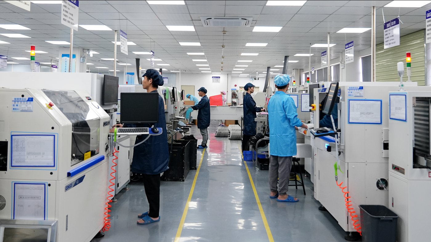
Wide view of PCB manufacturing workshop with operators and inspection benches

How Do We Review PCB Manufacturing Capability?

PCB capability depends on the full construction, not only on one headline parameter. A 32-layer rigid PCB, a 20 oz heavy copper board, a 0.10 mm laser via design, and a special laminate project may each require a different review path.

Our current FR-4 process specification separates standard process ranges from special-process review. The table below summarizes key items customers often ask about during supplier evaluation.

Capability Standard Process Special Process / Review
FR-4 layer count 1-10 layers 10-32 layers
Inner copper 0.5-5 oz 5-20 oz
Outer copper 1-5 oz 5-20 oz
Laser blind/buried via 0.10 mm Project construction must be reviewed
Minimum finished mechanical hole 0.20 mm 0.15 mm
Through-hole aspect ratio Up to 8:1 Up to 10:1
Inner trace/space 4/4 mil at suitable copper 3/3 mil at suitable copper
Outer trace/space 4/4 mil at suitable copper 3/3 mil at suitable copper
Surface finishes OSP, HASL, ENIG, ENEPIG, immersion silver, immersion tin, hard gold and others Project dependent

These values should be used as an early screening reference. Final manufacturability still depends on the complete stack-up, panel size, copper distribution, finished thickness, tolerance, surface finish, quantity, and inspection requirements.

Why Do Engineers Work With Us?

Engineering teams work with us because many PCB problems are easier to solve before production starts. We review the design package early so customers can correct unclear specifications, high-risk stack-ups, component sourcing gaps, or testing assumptions before they become schedule and reliability problems.

  • Gerber and drill-file completeness review.
  • Stack-up, material and finished thickness review.
  • Copper weight, spacing and impedance discussion.
  • Hole, via, blind/buried via and HDI structure review.
  • Surface finish and solderability review.
  • BOM sourcing and component availability checks.
  • SMT, THT/DIP and mixed-assembly process review.
  • Inspection and functional-test planning.
  • Prototype-to-production transition support.

This approach is especially useful for HDI, RF PCB, heavy copper PCB, metal-core PCB, ceramic PCB, rigid-flex PCB, dense PCBA, BGA assembly, fine-pitch components and projects with formal inspection documentation.

PCB engineers reviewing layout and stack-up files during DFM review

How Do We Support PCB Materials and Special Technologies?

Material selection affects thermal behavior, signal performance, dimensional stability, assembly reliability, and cost. We help customers match material choices to the electrical, mechanical, thermal, and supply-chain needs of the project.

  • Low-Tg, mid-Tg and high-Tg FR-4.
  • Halogen-free FR-4 and selected high-temperature material options.
  • Rogers 4003, Rogers 4350, Rogers 5880 and other RF laminate families.
  • Taconic, PTFE, Isola 370HR, Isola FR408HR and Nelco options.
  • Aluminum, copper and stainless-steel substrates for metal-core PCB.
  • Al2O3, AlN, ZrO2, Si3N4 and other ceramic substrate options by process type.
  • Flexible and rigid-flex materials for FPC and compact assemblies.

Material availability should be confirmed with the target thickness, copper type, layer structure, impedance target, quantity, and delivery requirement. For special laminates, we recommend confirming procurement before the layout is frozen.

How Do We Support Turnkey PCBA?

EBest Circuit can continue the project after bare-board fabrication, so customers do not need to coordinate separate PCB, component sourcing, and assembly suppliers for every build.

  • SMT assembly.
  • THT / DIP assembly.
  • Mixed SMT and through-hole assembly.
  • Component sourcing.
  • Customer-supplied components.
  • PCB with wire or cable assembly.
  • Box-build assembly.
  • Inspection and functional testing.

Customers can choose turnkey PCBA, consigned components, or hybrid sourcing. For turnkey projects, we handle PCB fabrication, component sourcing, assembly, and agreed testing. For consigned or hybrid builds, customers can supply controlled, programmed, allocated, or critical components while we support the remaining manufacturing scope.

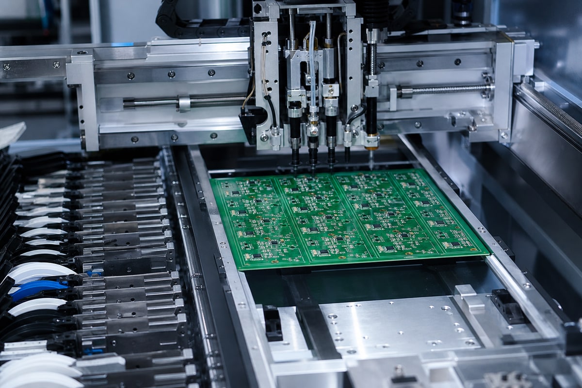
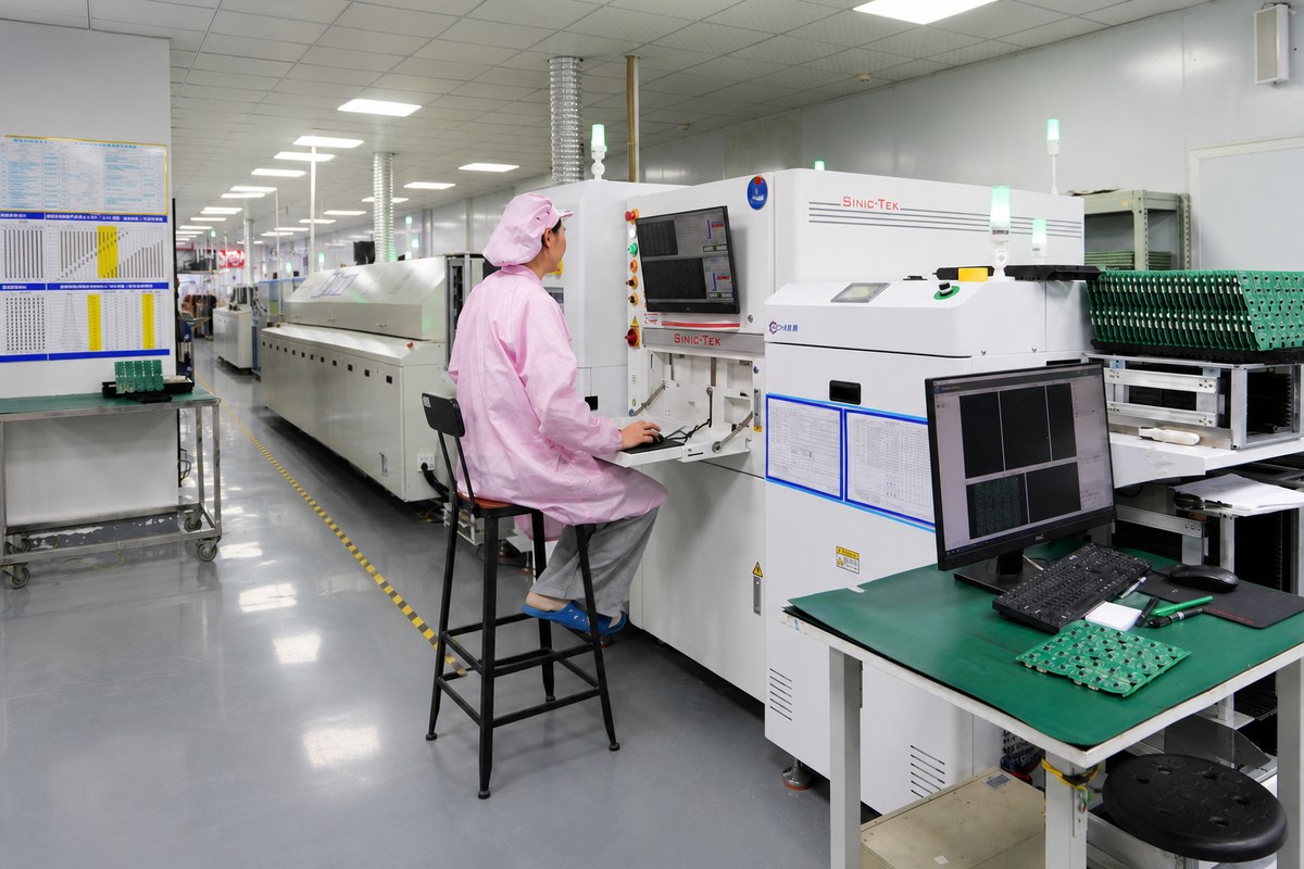
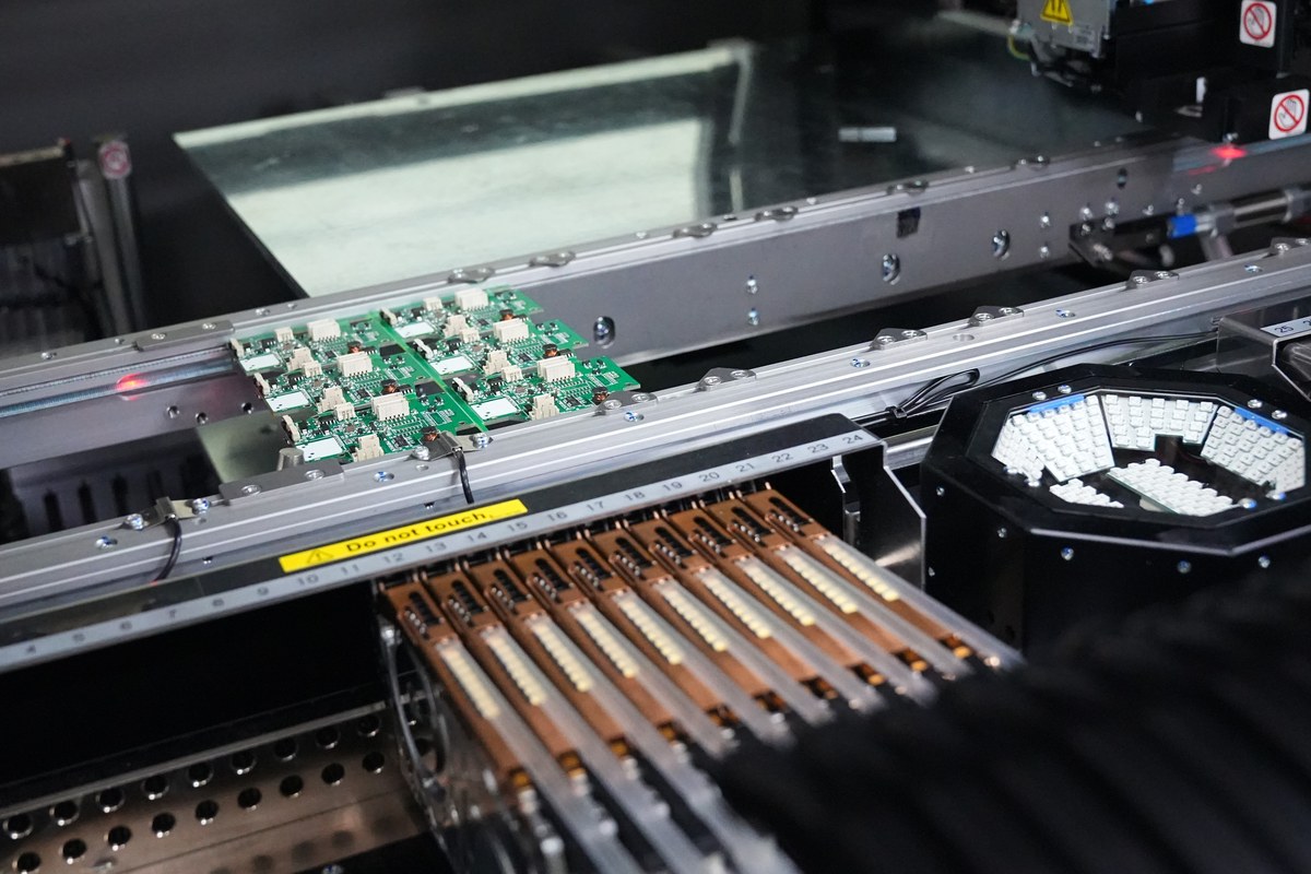
PCBA assembly line with populated circuit boards moving through production

What Quality Certifications and Standards Support Our Work?

Quality documentation matters when a PCB or PCBA supplier is part of a formal approval process. EBest Circuit company materials list ISO 9001:2015, ISO 13485:2016, IATF 16949, AS9100D, UL, RoHS, REACH and FPC SGS documentation.

Certification scope can vary by product, process, manufacturing route, and customer requirement. If your project requires a specific IPC class, certificate package, quality document, material record, inspection plan, or customer audit, include it in the RFQ so we can confirm the applicable path before production.

Certification or Compliance Item Typical Relevance
ISO 9001:2015 General quality management
ISO 13485:2016 Medical-device-related quality management
IATF 16949 Automotive quality management
AS9100D Aerospace-related quality system requirements
UL / UL E502832 UL recognition and product documentation
RoHS / REACH Environmental compliance support
FPC SGS documentation Supporting documentation for flexible PCB projects

How Do We Control PCB and PCBA Quality?

Quality control is built across incoming inspection, fabrication, assembly, final inspection, and shipment. The right inspection plan depends on the board type, component density, end application, and customer requirements.

For PCB fabrication, inspection and measurement may include:

  • AOI.
  • Electrical testing.
  • Flying probe testing.
  • Impedance testing.
  • Copper-thickness measurement.
  • Microsection inspection.
  • Hole-diameter measurement.
  • Dimensional measurement.

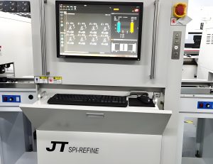
For PCBA production, inspection may include SPI, AOI, X-ray, first-article inspection, functional testing, and project-specific tests. A simple SMT assembly does not need the same test plan as a dense PCBA with BGA, fine-pitch ICs, programmed devices, firmware loading, or critical functional requirements.

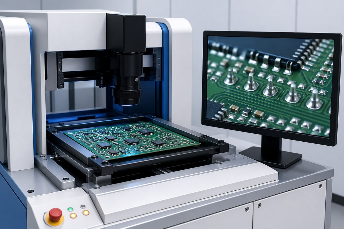
Engineer inspecting assembled printed circuit boards under microscope

What Testing and Inspection Methods Are Available?

Each test method is selected to control a specific manufacturing risk. Customers should specify required testing, fixtures, firmware, procedures, expected outputs, and pass/fail criteria where applicable.

Inspection / Test Main Purpose
AOI Checks visible PCB or assembly defects
Flying Probe / E-Test Detects opens and shorts
SPI Checks solder-paste deposition
X-Ray Inspects hidden solder joints such as BGA connections
Impedance Test Verifies controlled-impedance structures
Microsection Examines plated holes and internal construction
Copper Thickness Test Confirms copper thickness
Dimensional Measurement Checks mechanical dimensions
FAI / First Article Verifies the initial build before continuing
Functional Test Confirms agreed electrical or functional behavior
XJTAG Supports applicable boundary-scan or test requirements

Not every project needs every inspection method. The most efficient test plan is the one that matches the real product risk.

What Lead Time Should You Expect?

Lead time depends on layer count, material availability, copper thickness, board complexity, component sourcing, inspection requirements, testing scope, and production quantity. Prototype and volume production schedules should be reviewed separately.

Reference FR-4 prototype lead times in company materials include:

  • Single-layer PCB: 3-4 days.
  • 2-layer PCB: 4-6 days.
  • 4-6 layer PCB: 6-10 days.
  • 8-layer PCB: 10-14 days.
  • 10-layer PCB: 14-18 days.
  • 1+N+1 / 2+N+2 HDI: about 2.5-3.5 weeks.

For PCBA projects with customer-supplied components, reference prototype assembly lead times include about 1 week for components >=0402 without DIP, about 1-2 weeks for components >=0402 with DIP, about 1-2 weeks for components <=0201 without DIP, and about 1.5-2 weeks for components <=0201 with DIP. BOM purchasing can add time, especially when components are unavailable, allocated, obsolete, or long-lead.

What Should You Send for Engineering Review?

The fastest way to evaluate a PCB or PCBA project is to send the actual files and requirements. Partial files are useful at the early design stage, but a complete package gives a more reliable quotation and manufacturing plan.

For bare PCB review, send:

  • Gerber or ODB++ files.
  • NC drill files and drill table.
  • Stack-up and finished board thickness.
  • Material, copper weight and surface finish.
  • Impedance, via and tolerance requirements.
  • Quantity and target delivery date.
  • Required IPC class, certificates or inspection records.

For PCBA review, also send:

  • BOM.
  • Pick-and-place file.
  • Assembly drawing.
  • Component sourcing preference.
  • Programming requirements.
  • Functional-test requirements.
  • Expected prototype and production quantity.

If the design is still under development, send the files you already have. We can identify which specifications need to be confirmed before production.

Finished PCB and PCBA boards packed in anti-static bags for shipment

FAQ About Working With EBest Circuit

Can EBest Circuit support both PCB fabrication and PCBA assembly?

Yes. We support PCB fabrication, component sourcing, SMT assembly, THT/DIP assembly, mixed assembly, inspection, functional testing, and selected box-build requirements.

Can you review files before quotation?

Yes. Send Gerber files, drill files, stack-up, BOM, pick-and-place data, drawings, quantities, and test requirements. We can review manufacturability before quotation.

Can customers supply their own components?

Yes. Customers may choose turnkey PCBA, consigned components, or hybrid sourcing. Hybrid sourcing is useful when customers want to control critical ICs or programmed devices.

Can you support prototype builds before production?

Yes. We support prototypes, small-volume builds, and volume production. A project can move through prototype review, design updates, pilot production, and larger production batches.

Can customers arrange a factory audit?

Yes. Customers can arrange an audit as part of supplier qualification. Share the audit checklist, scope, preferred manufacturing site, and proposed date in advance.

What if a PCB is outside the standard process window?

Send the files for engineering review. Special-process items such as 3/3 mil features, 0.15 mm finished holes, high copper weight, more than 10 FR-4 layers, unusual thicknesses, or 10:1 aspect ratio need to be reviewed with the complete stack-up.

Start Your PCB or PCBA Project With EBest Circuit

If you are evaluating EBest Circuit as your PCB and PCBA manufacturing partner, send us the project data you already have. We can review the files, confirm the manufacturing path, raise technical questions, and prepare a quotation based on the actual build.

For bare PCB projects, send Gerber or ODB++ files, stack-up, material, copper weight, quantity, surface finish, and any inspection requirements. For PCBA projects, add the BOM, pick-and-place file, assembly drawing, sourcing preference, programming needs, and functional-test requirements.

Send your PCB or PCBA files to sales@bestpcbs.com for engineering review and quotation.


You may also like

Fiber Optic FPV Drones PCB Design and Manufacturing Guide

August 24th, 2026

A fiber optic fpv drones PCB connects the flight controller, camera or video processor, optical transceiver, power regulation, sensors, and motor-control interfaces in a compact airborne electronics system. The fiber carries optical data, but the PCB still has to manage high-speed electrical signals, switching noise, heat, vibration, connector stress, and strict weight limits.

The design should therefore be treated as a coordinated set of signal, power, mechanical, and manufacturing decisions. This guide focuses on the PCB and PCBA engineering needed for lawful industrial, inspection, research, and communications applications. Exact data rates, environmental limits, interfaces, and acceptance tests must be defined for each project.

Fiber Optic FPV Drones PCB with optical transceiver, flight controller, and fiber interface

What Is a Fiber Optic FPV Drones PCB?

A fiber optic FPV drones PCB is the board-level platform that routes control and video data between the drone electronics and an optical communication module. It may be one integrated assembly or several boards connected as a flight-control stack, camera board, optical-interface board, power board, and electronic speed controller system.

The optical fiber does not carry electrical power to the aircraft. A battery and local regulators still power the processor, sensors, camera, transceiver, and other loads. The PCB must keep those rails stable while motors and switching converters create rapid current changes. It must also preserve the electrical channel between the processor or video interface and the optical transceiver.

How Does a Fiber Optic FPV Drone Work?

A fiber-linked FPV platform converts electrical control and video data into optical signals, sends them through a lightweight fiber, and converts them back at the opposite end. The exact phrase fiber optic fpv drone how it works often leads readers to the link itself, but reliable operation also depends on the electronics around that link.

  1. The camera and sensors create video and flight data.
  2. The flight controller processes commands and sensor inputs.
  3. An electrical interface passes selected data to an optical transceiver or conversion module.
  4. The transceiver converts electrical data to light for transmission through the fiber.
  5. The ground-side unit performs the reverse conversion for the display and controller.

This arrangement can remove the primary control/video path from a conventional radio link, but it does not make the complete aircraft immune to every disturbance or failure. Power noise, damaged connectors, excessive fiber bending, processor faults, sensor errors, and mechanical stress can still interrupt the system.

Fiber optic FPV system architecture showing the drone PCB, optical link, and ground unit

Which Circuit Boards and Functional Blocks Make Up the System?

The system normally combines flight control, video, optical communication, power conversion, sensing, and motor interfaces. These functions can share one board, but separating them may simplify noise control, thermal management, service, and mechanical placement.

Board or Block Main Function PCB Design Focus
Flight controller Processes sensor data and generates control outputs Clean sensor power, stable clocks, short return paths, vibration-aware placement
Optical interface Converts electrical data to and from optical signals Differential routing, decoupling, connector retention, transceiver heat
Camera or video board Captures and conditions the FPV image stream High-speed interface integrity, low-noise power, compact interconnects
Power distribution and regulation Feeds logic, camera, optical module, and peripheral rails Current capacity, filtering, protection, thermal paths
ESC or motor interface Drives or commands the motors High-current loops, switching noise, MOSFET cooling, isolation from sensors

For a broader system comparison, our guide to the types of circuit boards used in drones explains how flight-control, power, camera, sensor, and communication boards divide the work.

What Makes an FPV Drone PCB Board Different?

An fpv drone pcb board must operate under tighter weight, space, vibration, and power-noise constraints than many stationary electronics. In a fiber-linked design, the optical interface adds another high-speed data path and a mechanically sensitive connection near a moving platform.

  • Mixed electrical environments: quiet sensors and high-speed data operate near motor switching and battery current.
  • Mass and balance: board dimensions, copper weight, connectors, shields, and the fiber assembly affect mechanical integration.
  • Limited cooling: airflow changes with enclosure, speed, board orientation, and nearby components.
  • Continuous movement: vibration can fatigue solder joints, connectors, cables, and unsupported components.
  • Service constraints: densely stacked boards need accessible test points and a clear replacement strategy.

These constraints should be set before schematic capture. Adding the optical module late can create blocked airflow, long data routes, poor connector access, or an unstable center of mass.

How Should an FPV Drone Controller PCB Handle the Optical Interface?

An fpv drone controller pcb should treat the optical transceiver as a high-speed electrical load with its own power, thermal, signal, and connector requirements. The fiber begins at the optical port; everything between the processor and that port is still an electrical PCB channel.

Start with the selected module datasheet and define its host interface, supply rails, peak current, reset behavior, clocking, connector, and thermal limits. Keep high-speed pairs short, maintain a continuous reference plane, and avoid stubs or unnecessary test pads. Place local decoupling close to supply pins and provide a low-inductance return path.

Connector orientation must be coordinated with the enclosure and fiber path. The optical connector or pigtail should not transfer repeated pull or twist directly into small solder joints. If the design uses a separate optical daughterboard, specify the board-to-board connector, retention method, mating cycle, and service access before layout.

Close view of an FPV drone optical interface PCB with transceiver and controlled routing

How Should Power Domains Be Separated from Motor Noise?

Power-domain planning should prevent motor and converter noise from disturbing the flight controller, camera, sensors, or optical interface. A single battery may feed every function, but that does not mean all loads should share the same unfiltered path.

  • Keep high-current battery and motor loops physically compact.
  • Separate sensitive regulators from switching nodes and hot power components.
  • Use the regulator vendor’s recommended input, output, and compensation layout.
  • Place high-frequency decoupling at the IC pins and bulk capacitance near load groups.
  • Do not split a reference plane beneath a high-speed signal simply to create visual separation.
  • Plan current return paths before routing signals between functional zones.

Power integrity should be checked during load transitions, not only at idle. The optical transceiver, processor, and camera may react differently to voltage droop or ripple. Test limits should come from the component datasheets and system specification rather than one generic ripple target.

Drone PCB power-domain layout separating motor current from flight-control and optical circuits

How Should High-Speed Video and Control Data Be Routed?

High-speed routes should be designed as transmission lines whose geometry, return path, vias, and connector launches are controlled from the processor to the optical module. The required impedance and matching tolerance depend on the actual electrical interface and component datasheets.

Practical layout checks include:

  • Define the stackup and target impedance with the PCB fabricator before final routing.
  • Keep differential-pair geometry consistent and avoid abrupt neck-downs.
  • Minimize stubs, layer changes, and unnecessary connector transitions.
  • Add nearby return vias when a high-speed pair changes reference layers.
  • Separate fast data from switching nodes, motor phases, and noisy clock sources.
  • Reserve test access that does not create an unacceptable discontinuity.

Our high-speed digital PCB design guide covers stackup, return paths, differential routing, vias, crosstalk, and power integrity in more detail. When waveform margin matters, an eye diagram can be combined with TDR, channel measurements, and functional testing under defined conditions.

What Does the Fiber Optic FPV Drone Cable Change Mechanically?

The fiber optic fpv drone cable adds bend-radius, strain-relief, routing, connector, and spool-integration requirements that must be resolved with the PCB and enclosure. The board should not become the mechanical anchor for an unsupported fiber path.

Define the minimum bend radius, connector or pigtail geometry, retention method, exit angle, and allowable movement from the chosen fiber and module documentation. Keep the path away from sharp board edges, propulsive components, hot surfaces, and service fasteners. If a separate spool or dispensing assembly is used, its loads should be carried by the mechanical structure rather than small PCB pads.

Mechanical review should also cover assembly sequence. A connector that is electrically correct may be unusable if it cannot be mated after the boards are stacked. A short flexible interconnect or daughterboard may improve serviceability, but it adds connectors and possible signal discontinuities that require validation.

Which PCB Stackup and Materials Fit the Design?

The stackup should be chosen from routing density, electrical interface speed, power-current needs, board thickness, weight, and manufacturing tolerance. There is no universal layer count or laminate for every fiber-linked drone controller.

Design Need Possible PCB Direction Decision Check
Compact controller with moderate routing density Multilayer FR-4 Reference planes, finished thickness, thermal margin, impedance feasibility
Fine-pitch processor or dense camera interface HDI construction when justified Escape routing, microvia structure, assembly yield, cost
Moving camera or constrained interconnect Flexible or rigid-flex circuit Bend zone, stiffener, dynamic-cycle requirement, connector reduction
Higher-current power section Localized heavier copper or separate power board Temperature rise, etching limits, weight, copper balance

Controlled impedance requires agreement on dielectric thickness, copper thickness, trace geometry, and material properties. Our impedance control PCB guide explains how design targets connect to fabrication and test coupons.

How Should Vibration, Heat, and Environmental Exposure Be Managed?

Reliability starts with the actual mounting, airflow, duty cycle, temperature, humidity, and vibration profile. A coating or stronger material cannot compensate for unsupported connectors, poor thermal paths, or components placed in high-strain areas.

  • Keep heavy components away from unsupported board edges where possible.
  • Use mounting-hole and keep-out geometry that avoids local copper or laminate stress.
  • Review connector retention and cable strain relief as part of the enclosure.
  • Provide copper area and thermal vias for regulators, processors, and power devices when the package guidance requires them.
  • Measure component temperatures in the real enclosure and operating airflow.
  • Select conformal coating or sealing only after checking connectors, sensors, optical surfaces, rework, and service requirements.

Board cleanliness matters if a coating will be applied. Flux residue or moisture trapped beneath a coating can create reliability problems instead of preventing them.

Which DFM and PCBA Checks Matter Before Production?

DFM and PCBA review should connect the schematic, layout, component data, mechanical model, and test plan before the first build. The review is most useful when it identifies risks that can still be changed.

  • Fabrication data: final Gerber or ODB++ data, drill files, stackup, controlled-impedance table, and board outline.
  • Assembly data: BOM with manufacturer part numbers, centroid file, polarity notes, approved substitutes, and special handling instructions.
  • Mechanical data: enclosure model, connector height, board stack spacing, mounting hardware, and fiber exit path.
  • Process checks: fine-pitch escape, solder-mask clearances, thermal-pad design, panelization, fiducials, and test-point access.
  • Supply checks: component lifecycle, optical-module availability, connector lead time, and traceable alternates.

If the design includes a dense image path, our camera PCB module guide provides related manufacturing and assembly considerations.

How Should the PCB Be Tested and Validated?

Validation should move from bare-board checks to assembled-board inspection and then to system testing under defined electrical and mechanical conditions. A board that powers on once has not yet demonstrated stable optical, control, sensor, and power performance.

Test Stage What It Checks Typical Evidence
Bare PCB Continuity, isolation, dimensions, holes, and controlled impedance when specified Electrical test record, dimensional inspection, impedance report or coupon data
PCBA inspection Placement, polarity, solder joints, bridges, voiding, and hidden connections AOI, X-ray where appropriate, visual inspection, reflow records
Power-up Rail sequence, current draw, ripple, reset, clocks, and thermal behavior Measured waveforms, current log, thermal measurements
Interface validation Camera, controller, sensor, and optical data paths Functional logs, error counters, waveform or channel measurements
System validation Operation in the intended enclosure, wiring, motion, and environment Approved test procedure and pass/fail report
Inspection and electrical testing of a fiber optic drone PCBA

FAQ About Fiber Optic FPV Drones PCB

  • Does the optical fiber replace every communication circuit?
    No. It can carry selected control and video data, but the system still needs processors, interfaces, sensors, local power, and possibly other links. The exact architecture depends on the product specification.
  • Does the PCB route optical signals as copper traces?
    No. Copper traces carry electrical signals to the optical transceiver. The transceiver converts those signals to light, which then travels through the fiber.
  • Is a high-frequency laminate always required?
    No. Material choice depends on the electrical interface, route length, loss budget, stackup, temperature, and fabrication tolerance. Multilayer FR-4 may be suitable for some designs, while others need a lower-loss construction.
  • Can the optical module share a regulator with the flight controller?
    Only if the load transients, ripple, sequencing, noise, and thermal limits remain within every component’s requirements. Separate filtering or regulation may be safer, but the decision should be verified by measurement.
  • What files are needed for PCB manufacturing and assembly review?
    Prepare fabrication data, drill files, stackup, impedance requirements, BOM, centroid file, assembly drawing, mechanical data, optical-module documentation, quantities, and the intended test plan.

How Can EBest Circuit Support Your Drone PCB Project?

A dependable fiber optic fpv drones PCB project needs the optical interface, flight-control electronics, power architecture, mechanics, and manufacturing data to agree before production. At EBest Circuit, we support PCB design review, PCB fabrication, component sourcing, PCBA assembly, impedance-related build requirements, and inspection for custom electronics projects.

Send your Gerber or ODB++ data, stackup, impedance table, BOM, centroid file, board dimensions, optical-module datasheet, quantities, mechanical constraints, and test requirements to sales@bestpcbs.com. We can review the manufacturing package and help prepare the board for prototype or production quotation.

You may also like

PCB Assembly France: Compare Suppliers and Get a Quote

August 24th, 2026

Choosing a supplier for PCB assembly France is not only a price decision. French engineers and buyers must protect design intent, component authenticity, build quality, delivery, and total landed cost—especially when comparing local, European, and overseas suppliers.

EBest Circuit (Best Technology) supports French PCB projects from its China-based PCB and PCBA factories. One commercial contact works with three engineers to coordinate DFM review, BOM optimization, PCB fabrication, component sourcing, assembly, inspection, and testing. The company supports prototypes and small batches as well as repeat production, including projects using heavy-copper, HDI, high-frequency, FPC, and rigid-flex PCB technologies.

Planning a PCB assembly project for France? Send your controlled PCB files, BOM, quantity, testing requirements, and delivery destination to sales@bestpcbs.com. EBest Circuit can review manufacturability and BOM risks before preparing an itemized quotation.

PCB assembly France
EBest Circuit’s SMT production environment supporting PCB assembly projects for French buyers.

What Should Buyers Expect from PCB Assembly France?

Expect a clearly defined manufacturing scope, named technical owners, controlled revisions, project-specific quality evidence, and a realistic landed delivery plan.

“PCB assembly France” can describe three sourcing models: production in France, production elsewhere in Europe, or an overseas supplier serving French customers. The best fit depends on the project—not the search phrase.

Before comparing prices, confirm who owns each part of the work:

  • Bare PCB fabrication and electrical testing.
  • Component procurement and approved substitutions.
  • SMT, through-hole, and manual assembly.
  • Programming, inspection, and functional testing.
  • Packaging, freight, customs, and import documentation.

For prototypes, fast engineering feedback and revision control often matter more than a small unit-price difference. For repeat orders, component continuity, process stability, traceability, and change control become more important.

EBest Circuit is an overseas option for French buyers, not a French factory or local legal entity. Buyers should therefore include international freight, customs, import responsibility, time-zone communication, and total landed lead time in the comparison.

PCB Assembly in Europe vs China: Which Model Fits French Buyers?

European production may fit projects that need frequent site access or very short transport. China-based production may fit projects that benefit from integrated PCB, component, assembly, and testing resources.

Buyer priorityEurope may fit whenChina may fit when
Engineering accessFrequent site visits are essentialOnline engineering reviews are sufficient
Supply scopeParts and processes are already localPCB, sourcing, PCBA, and test need coordination
CostProximity outweighs unit costRepeat-volume economics matter
Quality oversightOn-site review is preferredRemote records and traceability are accepted
DeliveryTransport time is the main constraintBuild time and sourcing efficiency matter more

Choose a nearby supplier when the design changes daily, physical collaboration is essential, or transport time dominates the schedule.

Consider a qualified China-based supplier when files are sufficiently mature, one team must coordinate several supply stages, or the project requires wider component-sourcing options. A hybrid model is also possible: keep unstable early builds close to the design team, then transfer a controlled package for repeat production.

In every model, compare the time from data release to usable boards at your facility—not only the factory build time.

PCB assembly France
Automated component placement on assembled PCBs during PCBA production.

What Files Are Needed for a PCB Assembly France Quote?

Send one revision-matched manufacturing package. Gerber files and a basic BOM are rarely enough for an accurate, production-ready quote.

Your package should include:

  • PCB data: Gerber or ODB++, drill files, board outline, stack-up, material, copper weight, finish, impedance, and special-process notes.
  • BOM: Manufacturer part numbers, quantities, reference designators, do-not-fit positions, approved alternates, and buyer-supplied parts.
  • Assembly data: Pick-and-place coordinates, rotations, board side, polarity, connector orientation, and assembly drawings.
  • Programming data: Firmware version, programming method, and verification instructions.
  • Quality requirements: IPC class if applicable, SPI, AOI, X-ray, electrical or functional test, report format, and acceptance limits.
  • Delivery requirements: Quantity, panelization preference, packaging, labeling, traceability, Incoterm, and destination.

Use the same revision identifier across every file. If the PCB data, BOM, centroid file, firmware, and drawings do not match, the supplier should issue an engineering query rather than guess.

EBest Circuit can provide a DFM pre-review and BOM risk or optimization list. The review may identify footprint conflicts, polarity questions, stencil risks, inaccessible test points, obsolete parts, long-lead components, and possible alternates. No substitute should be purchased without the buyer’s approval.

Before requesting a final price: Email the release package to sales@bestpcbs.com and ask EBest Circuit to separate confirmed parts, proposed alternates, unavailable items, tooling, testing, freight, and other one-time charges.

How Should French Buyers Compare PCB Assembly Quotes?

Compare equivalent scope and total landed project cost—not only the quoted price per assembled board.

Check these six areas in every quotation:

  • Bare PCB: Material, stack-up, finish, impedance, panelization, tooling, electrical test, and quantity.
  • Components: Exact part numbers, approved alternates, minimum purchasing quantities, excess material, and buyer-supplied parts.
  • Assembly: SMT sides, through-hole work, manual operations, stencil, setup, programming, and rework assumptions.
  • Quality: First-article approval, SPI, AOI, X-ray, functional testing, reports, and failure handling.
  • Delivery: Lead-time start point, production stages, freight method, customs, duties, VAT, and destination.
  • Records: Lot traceability, certificate of conformity, material records, and retention period.

Calculate the full project cost:

PCB + components + assembly + tooling + programming + testing + packaging + freight + import costs + expected delay or rework risk

Ask when the lead-time clock starts. It may begin after payment, after engineering questions close, or after all components arrive—not when the purchase order is sent.

Also evaluate the quality of the supplier’s response. A team that finds an incorrect footprint, unclear polarity, or risky substitute before production may save more than a small unit-price discount.

Which Quality Checks Matter for PCB Assembly France?

Use inspections that match the assembly risk, then request records that show what was checked, when it was checked, and how failures were handled.

Before production, confirm:

  • DFM and BOM review.
  • Incoming component and moisture-control procedures.
  • Stencil design and first-article approval.
  • Firmware, test limits, and fixture responsibility.

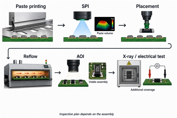
During SMT, 3D solder paste inspection can measure paste volume, area, and height before components are placed. At EBest Circuit, our 3D SPI capability supports 01005-class components. Our engineers confirm its suitability against the actual pad, stencil, package, and process design before production.

Placement controls should cover feeder setup, polarity, program approval, and first-piece verification. For reflow, EBest Circuit profiles new products using a physical board and retains process records. Buyers can request the project-specific thermal-profile evidence required by their quality plan.

After reflow, use the appropriate inspection method:

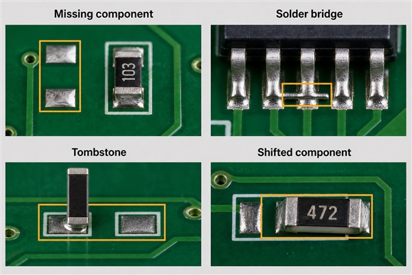
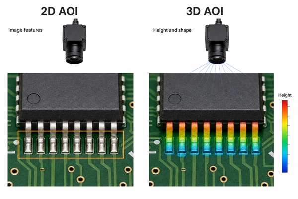
  • 3D AOI: Missing, wrong, rotated, reversed, lifted, bridged, tombstoned, or visibly under-soldered components.
  • X-ray: Hidden BGA, CSP, flip-chip, and similar joints.
  • Electrical or functional test: Circuit operation, firmware, interfaces, limits, and pass/fail results.

AOI and X-ray do not prove that a circuit functions. A complete test plan must define coverage, acceptance limits, records, and failed-unit disposition.

For medical, industrial-control, automotive-electronics, communications or 5G, and AI-hardware projects, verify that the factory, certification scope, inspection plan, and product controls match the actual application. Industry experience supports better engineering questions; it does not replace product-specific validation or the buyer’s regulatory responsibility.

PCB assembly France
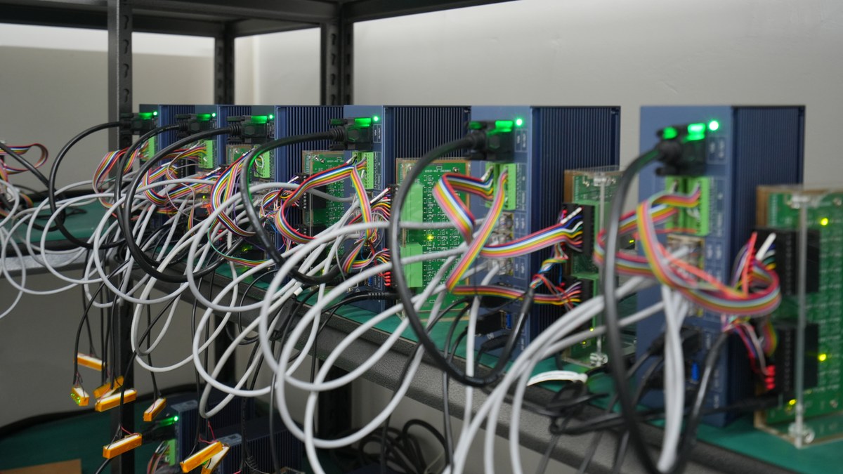
A powered multi-unit test setup used to support repeatable PCBA verification.

What Drives the Cost of Small Batch PCB Assembly in France?

Small-batch unit prices are driven by fixed engineering, setup, tooling, and test costs spread across fewer boards.

The largest cost drivers are:

  • PCB technology: Layers, material, copper weight, impedance, finish, vias, thickness, tolerances, and panel utilization.
  • Components: Price, shortages, minimum order quantities, lifecycle risk, alternates, and special handling.
  • Assembly: Placement count, package mix, board sides, fine-pitch devices, through-hole work, hand soldering, cleaning, coating, and mechanical assembly.
  • One-time work: DFM, stencil, programming, fixtures, first-article inspection, and test development.
  • Evidence: X-ray coverage, test time, serialization, traceability, and report requirements.
  • Schedule: Expedited material, priority production, express freight, customs, and delivery destination.

Buyers can reduce unnecessary cost by allowing the supplier to optimize panelization, resolving BOM risks before purchasing, approving alternates early, and reusing validated tooling when the revision permits. Do not remove an essential inspection or test simply to lower the quote.

EBest Circuit supports prototypes and small batches and offers an approximately 1.5-week rapid PCBA delivery target for suitable projects. This is a project-specific target, not a blanket guarantee. File readiness, component availability, PCB technology, test fixtures, factory capacity, freight, and customs all affect the actual delivery date.

How Should French Buyers Qualify an Overseas PCB Assembly Supplier?

Convert every important supplier claim into a document, record, sample, audit check, or pilot-build result.

Request the following evidence:

  • Legal company and manufacturing-site details.
  • Current certificates and their covered locations and scopes.
  • A sample DFM report and BOM risk or optimization list.
  • First-article, inspection, traceability, and nonconformance records.
  • Equipment capability matched to your board—not a generic machine list.
  • ESD, moisture, counterfeit-avoidance, calibration, and maintenance controls.
  • Named owners for engineering, sourcing, quality, and schedule escalation.

EBest Circuit holds ISO 9001, ISO 13485, IATF 16949, and AS9100D certifications. For a regulated project, ask us for the current certificate, covered manufacturing site, and applicable scope so your quality team can confirm that it matches the project requirements.

Our service model assigns one commercial contact supported by three engineers. DFM analysis, BOM optimization, and process recommendations are supported by team members with approximately 20 years of PCB, PCBA, and R&D experience. French buyers receive specific, documented engineering questions that are reviewed and closed before production.

EBest Circuit operates its own PCB and PCBA factories and works with more than 1,000 supply-chain partners. For each project, we can clarify which factory and approved supplier will handle every critical process or component, as well as how approved vendors and remaining materials are controlled.

For repeat production, test traceability during the pilot. Our digital workshop can retrieve material batch, product batch, production cycle, and progress information within five seconds. Select one serial or lot number, and our team can retrieve its related material, process, inspection, and shipment records for review.

PCB Assembly France Project Example: Prototype to Repeat Production

This anonymized example is based on a European customer project supported by EBest Circuit, showing how our engineering team clarified one unresolved requirement before material release and helped establish a controlled manufacturing package for repeat orders.

The project covered 30 assembled units using a three-layer flexible PCB. Recorded requirements included:

  • 12 µm base copper with additional plating.
  • Adhesive-free polyimide constructions.
  • Finished thickness of 0.20 mm ±0.03 mm.
  • ENIG and 50-ohm controlled impedance.
  • FR-4 stiffening below the component area.
  • Polyimide stiffening below the gold fingers.
  • EMI shielding film on both sides.
  • Components sourced by EBest Circuit.
  • Supplier-designed production panelization.

A 0.2–0.4 mm adhesive-tape requirement still needed clarification. The engineering query had to confirm its location, finished thickness, adhesive type, drawing reference, temperature exposure, and assembly sequence. Guessing could have affected fabrication, assembly, or the final mechanical fit.

Before moving from prototype to repeat production, the buyer and supplier should freeze:

  • PCB stack-up, impedance, finish, stiffeners, shielding, adhesive locations, and panel drawing.
  • BOM revision, purchased parts, approved alternates, and excess-material disposition.
  • Centroid data, orientations, stencil, work instructions, solder paste, reflow profile, and support tooling.
  • SPI, AOI, X-ray, dimensional, electrical, and functional-test requirements.
  • Engineering queries, deviations, repairs, and design corrections from the pilot.
  • Sample acceptance criteria and authorization to release the repeat order.

The customer benefit is controlled transfer. Repeat production uses one approved manufacturing package instead of relying on memory, email fragments, or an uncontrolled copy of the prototype files.

PCB assembly France
A repeat-unit validation setup illustrating the transition from prototypes to controlled production.

PCB Assembly France FAQs

Does EBest Circuit have a PCB assembly factory in France?

No. EBest Circuit (Best Technology) manufactures in China and serves French and other international customers. Buyers should include freight, customs, import responsibility, communication, and total landed lead time when comparing it with local or European suppliers.

What files should I send for a PCB assembly quote?

Send revision-matched PCB fabrication data, drill files, stack-up, BOM, centroid data, assembly drawings, programming files, test requirements, quantity, panelization instructions, packaging requirements, and delivery destination.

Can EBest Circuit support prototypes and small-batch PCBA?

Yes. EBest Circuit supports prototypes and small batches and can coordinate PCB fabrication, component sourcing, PCBA, inspection, and testing. Provide the expected repeat-production path so tooling, material, and quality controls can be planned from the start.

Can a PCBA order be delivered in 1.5 weeks?

Approximately 1.5 weeks is a rapid-delivery target for suitable projects, not a guaranteed lead time for every order. It depends on file readiness, component availability, PCB technology, engineering-query closure, testing, capacity, freight, and customs.

Which inspection reports should a French buyer request?

Request evidence matched to the project risk: DFM and BOM review records, first-article approval, SPI and AOI results, X-ray for hidden joints where applicable, reflow-profile evidence, functional-test results, lot traceability, and a certificate of conformity when contractually required.

Ready to review your PCB assembly project for France? Send your Gerber or ODB++ files, BOM, centroid data, assembly drawings, quantity, test requirements, and delivery destination to sales@bestpcbs.com. EBest Circuit (Best Technology) can provide a DFM pre-review, BOM risk and optimization list, recommended inspection plan, and an itemized PCB assembly quotation.

You may also like

Electronic Control Unit Board: From Design to Production

August 21st, 2026

An Electronic Control Unit board is the PCB or PCBA inside an automotive controller. It receives sensor data, runs control software, communicates with other vehicle modules, and drives loads such as motors, valves, relays, and solenoids. Unlike a general controller, an ECU board must remain stable under voltage transients, heat, vibration, moisture, and electromagnetic interference.

EBest Circuit supports ECU PCB design, fabrication, and assembly from engineering review and prototyping to volume production. For a project review, send the Gerber files, BOM, pick-and-place data, drawings, test requirements, quantity, and applicable automotive specifications to sales@bestpcbs.com.

Electronic Control Unit board installed in an automotive ECU enclosure

What Is an Electronic Control Unit Board?

An Electronic Control Unit board provides the electrical foundation of a vehicle control module. The bare PCB contains copper circuits, vias, component pads, and power and ground planes. After assembly, it becomes a PCBA containing processors, memory, communication interfaces, sensor inputs, protection devices, and output drivers.

Several related terms are often confused:

  • ECU: The complete control unit, including the PCBA, software, enclosure, connector, and thermal or sealing components.
  • ECM: An engine control module, which is one type of ECU.
  • ECU board: The bare PCB or assembled PCBA inside the unit.
  • Controller PCB: A broader category covering automotive and non-automotive control boards.

This distinction affects quotation scope. PCB fabrication, component sourcing, assembly, programming, coating, testing, and enclosure integration are separate deliverables unless the quotation states otherwise.

How Does an ECU Board Work?

An ECU board converts vehicle inputs into controlled outputs through several functional stages:

  • The power-input circuit filters the vehicle supply and protects the board from reverse polarity, overvoltage, ESD, and electrical transients.
  • Sensor-interface circuits condition signals from pressure, temperature, position, speed, current, and other sensors.
  • A microcontroller, processor, or system-on-chip compares the input data with programmed control logic.
  • Output drivers operate motors, injectors, pumps, valves, relays, lamps, or solenoids.
  • CAN, LIN, FlexRay, or Automotive Ethernet transceivers exchange data with other vehicle modules.
  • Diagnostic and watchdog circuits detect abnormal conditions and help the system enter a defined safe state.

The balance between these functions depends on the application. A body controller may contain many low- and medium-current outputs, while an ADAS controller places greater emphasis on processing speed, memory bandwidth, controlled impedance, and heat dissipation.

What Components Are Used on an Electronic Control Unit Board?

Most ECU boards contain the same functional blocks, although component count and performance vary.

Main functional components inside an automotive ECU board

Functional block Typical components Main concern
Power input TVS diode, filter, reverse-polarity protection Transients and voltage drop
Power conversion DC-DC converter, LDO, PMIC, inductors Efficiency, ripple, and heat
Processing MCU, MPU, SoC, FPGA Performance, safety, and lifecycle
Memory Flash, EEPROM, RAM Retention and programming
Sensor interface ADC, op-amp, filters, protection arrays Accuracy and noise
Communication CAN, LIN, FlexRay, Ethernet transceivers EMC and signal integrity
Output stage MOSFETs, relays, gate drivers, smart switches Current and junction temperature
Safety monitoring Watchdog and voltage supervisor Fault detection
Timing Crystal, oscillator, clock generator Stability and layout sensitivity

AEC-Q100, AEC-Q101, and AEC-Q200 may apply to ICs, discrete semiconductors, and passive components. These qualifications cover individual components rather than the complete ECU board, so PCB construction and assembly reliability still require separate controls.

Component selection should also consider operating temperature, package reliability, traceability, lifecycle, and approved alternatives. An electrically suitable component can still create production risk if it has limited availability or an unsuitable package.

Which Types of ECU Boards Are Used in Vehicles?

Different vehicle functions place different demands on the PCB.

  • Engine and transmission controllers: Accurate sensor measurement, fast processing, transient protection, and high-current outputs.
  • Body control modules: Multiple connectors and load drivers for lighting, doors, windows, seats, and comfort functions.
  • Chassis controllers: Fault detection and safety-related control for braking, steering, and suspension.
  • ADAS controllers: HDI routing, high-speed memory, controlled impedance, dense processors, and advanced cooling.
  • Battery management systems: Precise voltage measurement, isolation, creepage, clearance, and communication reliability.
  • Gateways and telematics units: Multiple vehicle networks, high-speed interfaces, security devices, and sometimes RF circuits.
  • Motor and inverter controllers: Strong immunity to high-current switching noise and high dv/dt environments.

An interior comfort controller does not need the same laminate, coating, thermal design, or validation plan as an engine-bay or battery-system controller. The mounting location, electrical load, and consequence of failure should guide the specification.

Which PCB Materials and Stackups Suit ECU Boards?

High-Tg FR-4 is commonly used because it supports multilayer construction and established automotive manufacturing processes. However, Tg alone does not determine suitability. The material review should also cover z-axis expansion, CAF resistance, moisture performance, copper adhesion, thermal decomposition, and compatibility with repeated assembly cycles.

Automotive ECU PCB materials and multilayer stackup cross-section

Requirement Suitable PCB construction
Standard body-control functions Multilayer high-Tg FR-4
Fine-pitch processors and memory HDI with microvias
High-current outputs Heavy copper or copper inlay
Automotive Ethernet Controlled-impedance multilayer PCB
RF or radar circuits High-frequency or hybrid laminate
Concentrated power-device heat Thermal vias, copper coins, or enclosure conduction

The approved stackup should define:

  • laminate grade;
  • core and prepreg thicknesses;
  • copper weight on each layer;
  • signal and reference-plane relationships;
  • controlled-impedance requirements;
  • via types and lamination cycles;
  • finished board thickness and tolerance.

Leaving these decisions open until production can change impedance, thermal performance, mechanical stability, and manufacturing yield.

How Should Power and Ground Be Designed on an ECU Board?

The power input must be designed for the vehicle supply rather than a stable bench source. Applicable transient conditions depend on the vehicle platform, voltage architecture, wiring harness, mounting location, and customer specification. Reverse polarity, cranking, overvoltage, and inductive-load disturbances should be translated into clear protection requirements before the schematic is released.

Automotive ECU PCB power input, grounding and high-current output layout

A typical power architecture includes:

  • input-current and reverse-polarity protection;
  • transient suppression and conducted-noise filtering;
  • regulated power rails and local decoupling;
  • controlled reset and power sequencing;
  • undervoltage and overvoltage monitoring;
  • clamping or freewheeling paths for inductive loads.

High-current returns should not share narrow copper paths with sensor grounds. However, splitting ground planes without analysing return currents can also increase noise and EMI. Power, digital, analogue, chassis, and load-return regions should therefore be connected through deliberate, low-impedance paths.

Copper sizing must account for current, pulse duration, voltage drop, temperature rise, vias, connectors, shunts, and neck-down areas. Widening one section of a trace does not solve a bottleneck elsewhere in the current path.

How Should Signal Integrity and EMC Be Controlled?

An ECU operates near motors, relays, switching converters, ignition circuits, wireless transmitters, and long wiring harnesses. EMC control must therefore begin at the connector and continue through placement, filtering, routing, grounding, shielding, and enclosure design.

Practical layout controls include:

  • place transient protection and filters close to external connectors;
  • route high-speed signals over continuous reference planes;
  • keep switching nodes compact and away from sensor and clock circuits;
  • control the geometry and return path of differential pairs;
  • minimise gate-drive and power-conversion loop areas;
  • place decoupling capacitors close to the relevant power pins;
  • avoid unnecessary stubs on communication buses;
  • provide test points for debugging and pre-compliance measurements.

CAN, LIN, and Automotive Ethernet have different termination, bandwidth, topology, and impedance requirements. They should not be treated as interchangeable two-wire connections.

Emission and immunity limits should be defined in the customer’s validation plan before the PCB layout is finalised. This allows the designer to reserve suitable filtering, shielding, grounding, component spacing, and test access instead of correcting EMC problems after the prototype has been assembled.

How Should Heat Be Managed on an ECU Board?

Thermal design should begin with the real power loss of regulators, processors, MOSFETs, smart switches, shunts, and relays. Average board temperature is not sufficient; each component must remain within its allowable junction temperature under the expected load and ambient conditions.

Common heat-control methods include:

  • wider copper areas around power devices;
  • thermal vias connected to useful internal or opposite-side copper;
  • heavier copper or copper inlays for high-current circuits;
  • exposed-pad packages with controlled solder-paste coverage;
  • thermal interface material between the PCBA and enclosure;
  • component spacing that avoids local hot spots.

Thermal vias provide limited benefit if they connect only to a small isolated copper area. Open vias beneath exposed pads may also draw solder away from the joint. Filled, capped, tented, or offset vias may be preferable depending on the package and assembly process.

Simulation should be followed by measurements on a representative assembly. Thermocouples, infrared imaging, and full-load operating tests help verify the complete heat path through the PCB, interface material, enclosure, and mounting structure.

How Is an Electronic Control Unit Board Manufactured?

An automotive PCB manufacturer should begin with a DFM review covering the stackup, copper balance, drill structure, impedance, panel design, assembly clearances, and test access. Conflicts between the Gerber files, BOM, drawings, and pick-and-place data should be resolved before materials are released.

Automotive ECU PCB assembly on an SMT production line

The main production stages are:

  • bare PCB fabrication and electrical testing;
  • solder-paste printing and SPI;
  • SMT placement and reflow;
  • AOI and X-ray inspection;
  • through-hole or selective soldering;
  • programming and serialisation;
  • ICT, boundary scan, or functional testing;
  • cleaning, conformal coating, or potting;
  • enclosure assembly and final inspection.

Large connectors, relays, transformers, and high-current terminals often require through-hole assembly. BGAs, QFNs, and bottom-terminated power packages generally require X-ray inspection because their solder joints cannot be fully evaluated by AOI.

If conformal coating is specified, the drawing should identify coating type, thickness, coverage, curing method, and keep-out areas. Connectors, programming contacts, grounding features, pressure ports, and selected test points may need to remain uncoated.

Which Tests and Standards Apply to ECU Boards?

No single standard covers the complete ECU board. The applicable combination depends on the vehicle manufacturer, mounting location, safety classification, electrical architecture, and product specification.

For a production-level overview, see our PCB assembly testing services guide.

Standard or control Application
ISO 26262 Functional safety of automotive electrical and electronic systems
ISO 16750 Electrical, mechanical, climatic, and chemical conditions
CISPR 25 Vehicle-component electromagnetic emissions
ISO 11452 Electromagnetic immunity
IPC-6012 Qualification and performance of rigid PCBs
IPC-A-600 Bare-board acceptability
IPC-A-610 Electronic assembly acceptability
IATF 16949 Automotive quality-management processes
AEC-Q100/101/200 Qualification of electronic components
PPAP Production-process and part approval

These documents serve different purposes. ISO 26262 addresses functional safety, while ISO 16750, CISPR 25, and ISO 11452 guide environmental and EMC validation. IPC standards cover PCB and assembly requirements. IATF 16949 applies to the manufacturing quality system, and AEC-Q specifications apply to individual components.

The customer should identify the applicable revisions, test severity, acceptance class, documentation requirements, and any OEM-specific additions before quotation. Without that information, two suppliers may quote very different inspection and validation scopes.

Automotive ECU board functional, thermal and CAN diagnostic validation

What Causes Electronic Control Unit Board Failures?

ECU failures often involve interactions between electrical stress, temperature, vibration, moisture, layout, materials, and manufacturing variation.

Failure symptom Possible cause Investigation or prevention
Intermittent reset Supply drop, ground bounce, cracked joint Review power integrity and solder joints
Communication loss Termination error, connector damage, EMI Test the bus, harness, and transceiver
Burned output stage Overcurrent, transient, inadequate cooling Check the load, clamping, copper, and heat path
Sensor drift Contamination, noise, unstable reference Inspect cleanliness, filtering, and grounding
BGA or QFN open Warpage, voiding, fatigue, board flex Use X-ray, cross-sectioning, or dye-and-pry
Internal PCB short CAF, moisture, contamination Review material, spacing, cleanliness, and humidity
Corrosion Residues, coating gaps, water ingress Improve cleaning, sealing, and coating control

Failure analysis should begin with operating history, fault codes, environmental exposure, and production-lot information. Electrical measurements can then be combined with X-ray, microscopy, cross-sectioning, thermal imaging, or material analysis.

Replacing the visibly damaged component may restore one board, but it does not prove that the underlying design, load, enclosure, or manufacturing issue has been corrected.

What Drives Electronic Control Unit Board Cost?

Cost is influenced by the complete manufacturing and validation package rather than PCB dimensions alone.

The main cost drivers are:

  • layer count and panel utilisation;
  • high-Tg, low-loss, CAF-resistant, or specialised laminates;
  • HDI, microvias, via filling, and sequential lamination;
  • controlled impedance and tighter tolerances;
  • heavy copper, copper inlays, and thermal structures;
  • automotive-qualified components;
  • X-ray, ICT, functional testing, and programming;
  • conformal coating, potting, and enclosure assembly;
  • PPAP documents and customer-specific reports;
  • prototype quantity and component availability.

Useful cost reductions include removing unnecessary HDI structures, improving panel utilisation, standardising material thicknesses, adding practical test access, and approving suitable component alternatives before shortages occur.

The lowest prototype price is not always the lowest production cost. Material substitutions, incomplete testing, poor component traceability, and repeated engineering changes can cost more than the initial saving.

What Should Buyers Check Before Ordering an ECU Board?

First confirm whether the quotation covers a bare PCB, assembled PCBA, programmed controller, or complete boxed unit. The scope should identify included materials, components, testing, documentation, fixtures, and engineering charges.

A complete quotation package should include:

  • Gerber or ODB++ data and drill files;
  • approved stackup and impedance requirements;
  • fabrication and assembly drawings;
  • BOM with manufacturer part numbers;
  • approved component alternatives;
  • pick-and-place data;
  • firmware and programming instructions;
  • test limits and expected outputs;
  • coating, potting, housing, and labelling requirements;
  • prototype and production quantities;
  • required standards, reports, and traceability.

Buyers should also review the supplier’s fabrication capability, SMT and through-hole processes, component controls, engineering response, inspection methods, change management, and automotive quality system.

IATF 16949 certification is relevant, but it should not be the only supplier-selection criterion. Confirm that the certification scope, production location, subcontracted processes, inspection equipment, and documentation system match the actual ECU project.

FAQs About Electronic Control Unit Boards

What does an Electronic Control Unit board do?

An ECU board receives sensor and network data, processes it through a microcontroller or processor, and controls vehicle loads. It also manages power conversion, communication, fault monitoring, diagnostics, and protection against electrical disturbances.

How many layers does an ECU PCB need?

There is no universal layer count. A simple controller may use four or six layers, while an ADAS, gateway, or processor-dense ECU may require additional layers or HDI. The decision should follow routing density, reference-plane needs, power distribution, EMC, and thermal requirements.

What PCB material is commonly used for ECU boards?

High-Tg FR-4 is widely used, but the exact grade depends on temperature, thermal cycling, humidity, CAF resistance, copper structure, and assembly conditions. Heavy-copper, HDI, low-loss, or hybrid constructions should be selected only when the project requirements justify them.

How are ECU boards tested after assembly?

Testing may include SPI, AOI, X-ray, programming verification, ICT, boundary scan, and functional testing. Automotive validation can add thermal cycling, vibration, humidity, electrical-transient, and EMC tests. The customer specification should define the conditions and pass limits.

What information is needed for an ECU board quotation?

For a bare PCB, provide fabrication data, stackup, drawings, material requirements, copper weights, impedance targets, quantities, and acceptance criteria. For PCBA, also provide the BOM, placement data, assembly drawings, programming files, test requirements, and coating or enclosure instructions.

An Electronic Control Unit board must combine protected power inputs, stable signal processing, reliable communication, thermal control, EMC performance, and traceable production. Material and process choices should follow the mounting environment, electrical loads, safety requirements, and validation plan rather than a generic automotive specification.

If you are looking for reliable OEM manufacturing, ODM production, prototype development, volume production, or a custom engineering solution, contact the EBest Circuit engineering team at sales@bestpcbs.com for technical support and a quotation.

You may also like

LED Symbol in Circuit: Polarity, Diagrams and PCB Design

August 17th, 2026

The led symbol identifies a light-emitting diode in a schematic, but reading it correctly requires more than recognizing the two outward arrows. A usable design must also preserve anode and cathode orientation, select a suitable current-control method, map the schematic pins to the correct PCB footprint, and communicate polarity clearly to assembly and inspection teams.

LED symbol in circuit with PCB and polarity design

What Is an LED Symbol?

An LED symbol is the schematic representation of a light-emitting diode. Its diode element indicates a polarized semiconductor junction, while two arrows pointing away from the device indicate emitted light. The bar side marks the cathode in the schematic; the opposite terminal is the anode. Designers commonly assign the reference designator D, such as D1 or D12, although some libraries use LED-specific prefixes.

The symbol is only one part of the component definition. A complete CAD record should also include the manufacturer part number, electrical model, package, pin numbers, PCB land pattern and assembly data. If the schematic symbol has anode on pin 1 but the footprint maps pin 1 to the physical cathode pad, the drawing can look correct while the assembled board is wrong.

What Do the Arrows on an LED Symbol Mean?

The two arrows show that the device converts electrical energy into emitted light. Their direction distinguishes the LED from a photodiode: LED arrows point outward, while photodiode arrows point toward the junction because a photodiode receives light. A standard rectifier or signal diode has no light arrows.

LED symbol compared with diode and photodiode symbols

Arrow direction describes optical function, not current direction. Conventional forward current enters the anode and leaves the cathode. The cathode bar remains the reliable schematic cue when the arrows are small or when a dense drawing is viewed at reduced scale.

How Does an LED Work in a Circuit?

An LED emits light when it is forward biased and current passes through its semiconductor junction. The supply must raise the anode above the cathode by approximately the device’s forward voltage, VF. Forward voltage varies with semiconductor material, color, current and junction temperature, so a nominal value from a generic chart is not a substitute for the selected LED datasheet.

A resistor, constant-current driver or regulated switching stage must control current. Connecting a bare LED directly across a stiff voltage source can produce thermal runaway or immediate overcurrent damage. For PWM dimming, verify peak current, duty cycle, driver timing and the LED’s pulsed-current limits rather than assuming that a low average current makes every pulse safe.

How Do You Identify LED Symbol Polarity?

In the schematic, the cathode is the terminal at the bar and the anode is the opposite terminal. On a common through-hole LED, the longer lead is often the anode and a flat on the body often indicates the cathode. These physical cues are useful during prototyping, but leads may be trimmed and package conventions can vary.

LED symbol polarity with anode cathode through-hole and SMD identification

SMD LED polarity marks are package-specific. A notch, chamfer, colored stripe, internal electrode shape or printed mark may identify one terminal, but the same-looking mark is not guaranteed to mean the same thing across suppliers. Confirm the polarity diagram and recommended land pattern in the exact manufacturer datasheet, then make the schematic pin numbers, footprint pad numbers, silkscreen and pick-and-place rotation agree.

How Is an LED Symbol Used in a Circuit Diagram?

The led symbol circuit connection should make four relationships unambiguous: the drive source, the current-control element, the return path and the polarity. A simple indicator may place the LED and resistor between a logic output and ground. A low-side transistor driver places the LED load toward the supply and switches the return path. A high-side driver reverses that arrangement. In each case, the symbol orientation must reflect the intended conventional current path.

Net labels should identify important rails and control signals, while reference designators allow the BOM, placement file and test procedure to refer to the same component. When several colors or status channels are present, include color or function in the schematic notes, such as STATUS_GREEN or FAULT_RED, rather than expecting assembly staff to infer function from the symbol.

What Is the Difference Between an LED, Diode and Photodiode Symbol?

Device Symbol cue Primary circuit role Design detail to verify
Standard diode Diode element without light arrows Rectification, clamping or switching Forward current, reverse voltage and recovery behavior
LED Two arrows pointing outward Light emission, indication or illumination Forward voltage, current, color, optical output and thermal limit
Photodiode Two arrows pointing inward Optical sensing Bias mode, dark current, spectral response and amplifier interface

A schematic library should not reuse one symbol interchangeably for all three devices. Even when the footprint is similar, their electrical limits, test conditions and functional intent differ. Clear symbols also reduce review errors when a design contains emitters and optical receivers in the same circuit.

What Do Single-Color, Bicolor and RGB LED Symbols Show?

A single-color LED normally has one junction and two pins. A two-lead bicolor LED can contain two dies connected in inverse parallel; reversing current changes the active color. A three-lead bicolor device may use a common anode or common cathode. RGB LEDs commonly have four leads for red, green and blue channels plus a shared terminal, although addressable RGB packages may integrate a controller and use power, ground and data pins instead.

The schematic must show the actual internal connection. A generic three-diode drawing cannot tell assembly or firmware teams whether the package is common-anode, common-cathode or independently connected. Use the selected part’s pin numbering, give each color channel its own current-control element when required, and verify that the PCB footprint orientation matches the datasheet top-view or bottom-view convention.

What Information Does the LED Symbol Not Show?

The graphic does not specify forward voltage, rated current, luminous intensity, wavelength, viewing angle, reverse-voltage limit, ESD sensitivity, package dimensions or thermal resistance. It also does not establish whether the component is suitable for reflow, wave soldering, hand soldering or a particular cleaning process.

The BOM and datasheet must carry those requirements. For color-critical products, define wavelength or chromaticity and binning rather than using only “red” or “white.” For brightness matching, state the relevant optical bin and test current. For power LEDs, include the thermal-pad connection and maximum junction-temperature calculation. The symbol communicates connectivity; it does not replace component qualification.

How Do You Calculate an LED Current-Limiting Resistor?

For a simple DC circuit, calculate the series resistor with R = (VS – VF) / IF. If a 5 V rail drives an LED with a 2.0 V forward voltage at 10 mA, the calculated resistance is 300 ohms. Selecting the next higher standard value, such as 330 ohms, reduces current slightly and provides margin for supply and forward-voltage tolerance.

LED symbol circuit with current limiting resistor formula

Check resistor dissipation with P = I2R and apply a sensible derating margin. Calculate worst cases using maximum supply voltage and minimum LED forward voltage for peak current, then minimum supply voltage and maximum forward voltage for minimum brightness. Separate current control is normally preferred for parallel LED branches because normal VF variation can make one branch take disproportionate current.

How Should an LED Footprint and Polarity Mark Be Designed on a PCB?

Start with the manufacturer-recommended land pattern, then check courtyard, solder-mask expansion, paste apertures and component-to-component spacing against the assembly process. Map anode and cathode pin numbers explicitly between the schematic and footprint. A pin-1 convention is useful only when it agrees with the package drawing and does not conceal the electrical polarity.

Place a visible cathode or anode cue on the silkscreen without printing over exposed copper or solderable pads. If board density removes the silkscreen mark, preserve polarity in the assembly drawing and fabrication documentation. The silkscreen PCB design guide explains practical text and clearance controls. For low-power indicators and control panels, a conventional FR4 printed circuit board is usually appropriate. The footprint still needs enough thermal relief for solderability and enough copper to support the expected current.

How Are SMD and Through-Hole LEDs Assembled?

SMD LEDs are placed from centroid data and package rotation, then reflowed according to the component’s moisture sensitivity, peak-temperature and time-above-liquidus limits. Through-hole LEDs require controlled insertion height, lead forming, polarity checks and either selective, wave or hand soldering. A spacer or mechanical fixture may be needed when optical alignment to a light pipe or panel opening matters.

AOI can verify component presence, orientation marks and visible solder joints, but optical inspection alone does not prove color, brightness or electrical function. Hidden thermal pads may justify X-ray, while a functional test should energize channels at controlled current and confirm the intended color and response. EBest Circuit (Best Technology) supports SMT, THT and mixed assembly, with components down to 01005 where the design and process allow; inspection can combine 3D SPI, AOI, X-ray and functional testing according to the actual risk.

For production that needs component sourcing, placement and test under one controlled workflow, the PCB assembly service covers both fabrication and assembly coordination. The BOM should identify the approved LED manufacturer part number, package, color/bin requirements and permitted substitutes so that a visually similar but electrically different LED is not installed.

What Causes an LED Circuit to Fail?

  • Reverse installation: schematic-to-footprint mapping, pick-and-place rotation or manual insertion places the cathode on the anode pad.
  • Excess current: the resistor or driver was selected from typical values without worst-case supply, temperature and forward-voltage limits.
  • Poor thermal path: a power LED’s thermal pad, copper area, dielectric and heat-sink interface cannot keep junction temperature within limit.
  • Inadequate ESD control: handling or test equipment damages the junction before final functional test.
  • Solder defects: insufficient paste, tombstoning, voiding, cold joints or excessive reflow exposure reduces electrical or thermal reliability.
  • Uncontrolled substitution: a replacement part has different polarity marking, pinout, optical bin or footprint dimensions.

Power LEDs need a board selected for the complete thermal path, not just the substrate name. A metal-core PCB can shorten the path from LED pad to heat sink; EBest Circuit (Best Technology) lists MCPCB thermal conductivity from 0.8 to 3.0 W/mK, subject to stack-up and engineering confirmation. For higher insulation or power-density requirements, a high-power LED ceramic PCB may provide a different thermal and dielectric balance.

LED PCB materials including FR4 metal core and ceramic boards

Where Are LEDs Used on PCBs?

Low-current LEDs provide power, status, fault and communication indicators. Backlight and user-interface boards distribute many LEDs behind light guides or diffusers. Industrial controls use optically visible state confirmation, while sensing systems combine emitters with photodiodes or phototransistors. Automotive, medical and instrumentation products may require controlled color, luminance uniformity, lifetime and environmental validation.

High-power lighting, UV curing, infrared illumination and machine vision place greater demands on current regulation and heat extraction. In these products, the led symbol remains simple, but the board may require an MCPCB, ceramic substrate, thermal vias, direct thermal pads or a mechanically controlled heat-sink interface. Material selection should follow the allowed junction temperature, dissipated power, electrical isolation and assembly process.

FAQ About LED Symbols

Which side of the LED symbol is positive?

The anode is the positive side during normal forward operation. The cathode is the side at the bar in the schematic. Always confirm the physical package mark and pin numbering in the selected component datasheet.

Does the LED symbol show the color?

No. Color may be added as a schematic note or component value, but the symbol itself does not guarantee wavelength or optical bin. Those details belong in the BOM and approved part specification.

Can an LED be connected without a resistor?

Only when another circuit element safely regulates current, such as a constant-current LED driver or a source with an intentionally limited output. A bare LED should not be connected directly across a low-impedance voltage rail.

Is an SMD LED polarity mark universal?

No. Package marks differ among manufacturers and package families. Use the exact datasheet polarity and land-pattern drawing rather than relying on a remembered stripe or notch convention.

Why does an LED work in the prototype but fail after assembly?

Common causes include reversed footprint mapping, pick-and-place rotation, substitute-part pinout differences, reflow damage, ESD, solder defects and insufficient thermal dissipation. Compare the schematic, footprint, BOM, placement file and assembly drawing as one linked data set.

Conclusion

Reading an LED schematic is straightforward once the outward light arrows and cathode bar are recognized, but a reliable board also needs correct pin mapping, controlled current, clear polarity marking, a validated footprint and suitable thermal construction. Treat the symbol, datasheet, BOM, placement data and PCB documentation as one consistent definition.

EBest Circuit (Best Technology) can support FR4, metal-core, ceramic PCB and complete PCBA requirements for LED products. For engineering review or a manufacturing assessment, contact sales@bestpcbs.com.

You may also like

Multi Chip Module: Packaging, Design and PCB Integration

August 17th, 2026

A multi chip module places two or more semiconductor dies on a shared substrate so that the completed package can operate as one component. The approach can shorten critical connections, combine dies made with different processes and reduce the area required on the system board. Those benefits are not automatic: substrate technology, die attachment, power delivery, heat flow, test coverage and the PCB interface must be designed as one system.

Multi Chip Module: Packaging, Design and PCB Integration

What Is a Multi Chip Module?

A multi chip module, or MCM, is an electronic package or module containing multiple interconnected semiconductor dies. Logic, memory, analog, RF, sensor or power functions can share one package substrate. The module presents an external interface such as BGA balls, LGA lands or leads, allowing the system to handle it as a single component.

The defining point is the packaging hierarchy. Bare dies and their internal connections belong to the MCM. The larger board that receives the completed module is the system PCB. A board carrying several conventionally packaged ICs is a PCB assembly, but it is not automatically an MCM. Modern terminology overlaps with system-in-package and chiplet packaging, so the physical implementation and functional partition matter more than the label alone.

How Does a Multi Chip Module Work?

Each die performs a defined function and communicates through conductors in or on the shared substrate. Wire bonds can connect die pads to substrate pads. Flip-chip bumps can connect a die face-down to fine-pitch routing. An interposer or redistribution layer can provide much denser die-to-die paths than a conventional system PCB.

Multi chip module structure with bare dies package substrate BGA and system PCB

The substrate redistributes thousands of fine die connections to an external pitch that assembly equipment and the system PCB can support. It also carries power and ground, supports decoupling, controls impedance and provides part of the thermal path. Encapsulation, a lid, underfill or a heat spreader may protect the dies and stabilize the structure. The finished module is then soldered or mechanically connected to the system board.

What Are the Main Multi Chip Module Packaging Types?

Traditional multi chip module packaging is classified by how the interconnect substrate is made. MCM-L uses laminate technology, MCM-C uses ceramic processing and MCM-D uses deposited thin-film conductors and dielectrics. Modern packages may add silicon or organic interposers, redistribution layers, embedded bridges, fan-out structures or vertical stacking.

The class name does not fully define performance. A fine-line build-up laminate can outperform an older laminate construction, while a ceramic substrate may be chosen for dimensional or thermal reasons rather than maximum routing density. Die I/O pitch, signal speed, power density, module size, production volume and test strategy must be evaluated together.

How Do MCM-L, MCM-C and MCM-D Compare?

The practical decision starts with routing density, thermal expansion, heat flow and process maturity. The table summarizes the main differences without treating one technology as universally superior.

Type Substrate and process Typical strengths Primary constraints
MCM-L Organic laminate fabricated with advanced PCB or build-up processes Established supply chain, larger formats, practical multilayer routing and cost scaling CTE, moisture behavior, warpage and fine-feature limits depend on material and buildup
MCM-C Multilayer ceramic, commonly co-fired or thick-film processed Dimensional stability, electrical insulation, temperature capability and controlled material properties Higher material/process cost, brittle handling and shrinkage control
MCM-D Deposited thin-film metal and dielectric layers on a rigid base Fine routing, small vias and short high-performance interconnects Process complexity, equipment cost, layer buildup time and yield sensitivity
Comparison of MCM-L MCM-C and MCM-D multi chip module types

An MCM-L may use a multilayer FR4 PCB-like process when its electrical and thermal limits are appropriate. MCM-C can use a ceramic PCB or ceramic circuit substrate when insulation, dimensional stability or heat transfer justifies it. MCM-D is closer to thin-film microfabrication than ordinary PCB manufacturing.

What Is a Wafer Level Multi Chip Module?

A wafer level multi chip module uses wafer-level redistribution, fan-out or stacking processes to integrate multiple dies before the final package is completed. In a fan-out flow, known-good dies can be placed in a reconstituted wafer or panel, embedded in molding compound and connected with redistribution layers. Wafer-level system-in-package processes can place dies, passives or sensors side by side and can also support stacked configurations.

WMCM is not one fixed construction. The term may describe different multi-die wafer-level implementations, so package drawings must define die placement, redistribution layers, vertical connections, external ball pattern and thermal structure. It should not be used as a synonym for every MCM. The important distinction is that wafer-level processes form much of the package interconnect before singulation, unlike a laminate module assembled as an individual substrate.

What Matters in Multi Chip Module Design?

Multi chip module design is a chip-package-board co-design problem. Optimizing only die placement can leave an unrouteable substrate, an unstable power network or a poor thermal path. Start with the complete connectivity, power map, heat sources, package outline, external I/O and assembly constraints.

  • Die placement: keep high-bandwidth die pairs close, but reserve room for escape routing, decoupling, keepouts, underfill flow and heat spreading.
  • Signal integrity: control impedance, return paths, crosstalk, discontinuities and skew across die bumps, substrate routing, package balls and PCB traces.
  • Power integrity: size power/ground planes, place decoupling by frequency and current demand, and model simultaneous switching noise and voltage drop.
  • Thermal design: calculate die-level power maps rather than using only package-average power. Local hotspots can dominate junction temperature.
  • Mechanical design: review die size, substrate thickness, CTE mismatch, lid stiffness, underfill, molding and board attachment for warpage and fatigue.
  • Test access: plan die screening, boundary scan, package test, thermal monitoring and system diagnostics before routing is fixed.
Multi chip module electrical routing power delivery and thermal design

Short internal connections can reduce parasitic resistance, inductance and capacitance, but density also makes coupling and current concentration harder to control. Package and PCB models should therefore be analyzed together for fast interfaces. The same return-path discipline described in high-speed digital PCB design remains relevant after the signals leave the package.

How Is a Multi Chip Module Connected to a PCB?

The finished MCM commonly uses a BGA or LGA interface. Its ball or land map fans out into the system PCB through dog-bone vias, via-in-pad structures or microvias. The correct escape pattern depends on pitch, ball diameter, pad design, layer count, signal class, power distribution and assembly process. High-I/O modules can require an HDI PCB with laser-drilled microvias and sequential buildup.

The PCB stack-up must preserve return paths under high-speed signals, provide low-impedance power delivery and conduct heat away from the package. Thermal vias, internal copper planes, local copper density and a chassis or heatsink interface may all contribute. The board should also account for package warpage, component keepouts, rework clearance and the soldering profile.

Assembly data must identify package outline, pin-one orientation, paste stencil design, moisture sensitivity, reflow limits and inspection requirements. Very dense BGA interfaces usually need X-ray because optical inspection cannot see the internal solder joints.

How Do MCM, Chiplet, SiP and Monolithic IC Differ?

These terms describe different levels of integration. A chiplet is a die intended to be combined with other dies. An MCM is the package or module that interconnects multiple dies. A system-in-package usually emphasizes a complete system function and may include dies, passives, sensors, filters or MEMS. A monolithic IC integrates its functions on one die.

Term Physical meaning Design implication
Monolithic IC Functions fabricated on one semiconductor die Very short on-die links, but die size, process compatibility and yield constrain integration
Chiplet A modular die designed for multi-die integration Requires a defined die-to-die interface and compatible package architecture
MCM Multiple dies interconnected on a shared substrate or interposer Package-level electrical, thermal, mechanical and test co-design is essential
SiP Multiple functional elements combined as a packaged system May include MCM structures plus passives, sensors, RF filters or other components

The phrases multi chip module vs MCM do not describe competing technologies; MCM is simply the abbreviation. Multi chip module vs chiplet is different: the chiplet is one building block, while the MCM is an integration vehicle that may contain several chiplets or conventional dies.

Why Do MCM GPUs Support Continued Performance Scalability?

GPU and accelerator designs use multiple compute dies or chiplets to increase compute resources without making one monolithic die continually larger. Specialized dies for compute, cache, memory interfaces and I/O can be manufactured with process technologies suited to each function, then connected in an advanced package. This can improve design reuse and can reduce the yield penalty associated with a very large die.

Scalability still depends on the interconnect. Bandwidth, latency, synchronization, cache coherence, memory placement, package power and cooling determine whether additional dies deliver useful performance. AMD, for example, describes current accelerator architectures that connect GPU chiplets, high-bandwidth memory, cache and I/O through on-package Infinity Fabric links. The package does not remove the need for efficient workload partitioning or software support.

MCM GPU designs create a system tradeoff rather than a guarantee that adding dies will scale performance linearly. More dies can increase communication traffic and hotspot interaction, so architecture, packaging and cooling must advance together.

Where Are Multi Chip Modules Used?

Multi chip modules are used when several functions need a compact, high-bandwidth or application-specific connection. The implementation varies widely by industry.

  • High-performance computing: processors, GPUs, accelerators, cache and high-bandwidth memory packages.
  • RF and wireless: power amplifiers, switches, filters, control ICs and passive networks in compact front-end modules.
  • Automotive and industrial electronics: sensing, control, radar, power management and computing modules that require defined thermal and mechanical performance.
  • Medical and sensor systems: mixed-signal processing, sensing and communications integrated within a small package.
  • Aerospace and defense: dense computing or RF functions where size, weight, interconnect length and environmental qualification matter.

An intelligent power module may also integrate control and power semiconductor functions, but IPM and MCM are not interchangeable labels. The package construction, insulation structure, current path and thermal interface must be examined rather than inferred from the name.

What Can Go Wrong in Multi Chip Module Packaging?

Adding dies and interfaces creates more points that must be controlled. A design can be electrically correct and still fail because heat, stress, materials or test coverage were incomplete.

  • Known-good-die risk: one defective die can reduce the yield and value of an otherwise completed module.
  • CTE mismatch: silicon, organic laminate, ceramic, copper, molding compound and the system PCB expand differently during processing and operation.
  • Warpage: uneven materials, copper distribution or cure shrinkage can distort the substrate and disturb bump or BGA coplanarity.
  • Interconnect defects: non-wet joints, voids, opens, shorts, bond lift, bump fatigue and underfill voids may be hidden from optical inspection.
  • Electrical coupling: dense signal, power and ground structures can create crosstalk, return-path breaks, resonances and simultaneous switching noise.
  • Thermal interaction: one die can heat neighboring dies, while a package-average temperature hides a local hotspot.

Reliability is therefore conditional. Shorter connections can reduce some parasitics and board-level joints, but an MCM does not automatically outlast a single-die package. Material characterization, simulation, controlled assembly and qualification determine the result.

How Are Multi Chip Modules Inspected and Tested?

Inspection should follow the structure from die to system board. Wafer probing and known-good-die screening reduce the chance of packaging defective silicon. During module assembly, optical inspection can verify placement and wire bonds, while X-ray can reveal hidden bumps, BGA joints, bridges, opens and void patterns. Scanning acoustic microscopy may be used to detect delamination or underfill defects.

X-ray inspection of a multi chip module mounted on a PCB

Electrical tests include continuity, shorts, parametric checks and functional operation. Boundary scan can improve access when physical probing is limited. Thermal cycling, temperature-humidity, high-temperature operating tests, mechanical stress and power cycling are selected according to the application and dominant failure mechanisms. At the system-board level, PCB assembly controls such as solder paste inspection, AOI, X-ray and functional testing verify the module-to-board interface. The existing guide to X-ray inspection in PCB assembly explains the value of hidden-joint imaging in more detail.

What Should Multi Chip Module Manufacturers Coordinate with PCB and PCBA Teams?

Multi chip module manufacturers and system-board teams must exchange interface data early. The package outline, ball map, pin functions, pitch, pad recommendation, allowed via structures, power map, thermal resistance model, warpage limit, moisture classification and reflow window affect PCB layout and assembly. Signal models and power-delivery models are needed when the module carries fast interfaces or high transient current.

The PCB team should return the proposed stack-up, fan-out geometry, impedance targets, plane assignment, thermal-via design and mechanical constraints. The assembly team should confirm stencil strategy, paste type, placement support, reflow profile, X-ray criteria, cleaning limits and rework access. Revision control is critical: a changed ball assignment or package drawing can invalidate both layout and test fixtures.

EBest Circuit (Best Technology) supports the PCB and PCBA side of this integration. Published capabilities include HDI line/space down to 2/2 mil, HDI holes down to 0.10 mm and BGA pitch down to 0.25 mm. Maximum capability depends on material, layer stack-up, board dimensions, design complexity, production quantity and engineering review. These capabilities do not mean EBest Circuit fabricates semiconductor dies or wafer-level MCM packages; the scope is the supporting PCB, ceramic circuit and board-level assembly work.

FAQ About Multi Chip Modules

Is a multi chip module the same as a chiplet?

No. A chiplet is a modular die. A multi chip module is the package or assembly that interconnects multiple dies; it may contain chiplets, conventional dies or both.

Is MCM the same as multi chip module?

Yes. MCM is the standard abbreviation for multi chip module. The exact physical construction still needs to be defined because MCM-L, MCM-C, MCM-D and wafer-level designs use different processes.

Can a multi chip module use both wire bonding and flip chip?

Yes. A heterogeneous module can use different attachment methods for different dies when the substrate layout, assembly sequence, wire clearance, underfill and thermal process are compatible.

What does “MCM GPU multi chip module GPUs for continued performance scalability” mean?

It refers to partitioning a GPU or accelerator across multiple compute, cache, memory or I/O dies and connecting them in one advanced package. Continued performance scaling depends on die-to-die bandwidth, latency, power, cooling and software efficiency, not only the number of dies.

Is wafer level multi chip module packaging the same as MCM-L?

No. MCM-L is based on a laminate substrate. Wafer-level multi-die packaging typically uses redistribution, fan-out, molding or stacking processes formed at wafer or panel scale before final singulation.

Can a finished MCM be assembled on a standard PCB?

Sometimes. The external pitch, I/O count, power, thermal load and signal speed determine whether a conventional multilayer board is sufficient or an HDI, high-frequency or ceramic solution is required.

Conclusion

A multi chip module can combine specialized dies, shorten internal connections and reduce system-board area, but its value depends on coordinated package, thermal, test and PCB design. MCM-L, MCM-C, MCM-D and wafer-level approaches solve different density, material and manufacturing problems. When a completed module needs an HDI, FR4 or ceramic system board and controlled PCBA integration, EBest Circuit (Best Technology) can review the PCB-side construction and assembly requirements. Contact sales@bestpcbs.com.

You may also like

Laser Diode Driver Board: Design, Layout, and Manufacturing

August 15th, 2026

A laser diode driver board converts a power supply and control command into accurately regulated diode current. A reliable board must do more than turn the laser on: it must limit current, control startup and shutdown, suppress electrical transients, manage heat, and provide testable interfaces. This guide connects those operating requirements to circuit design, PCB layout, prototyping, fabrication, assembly, inspection, and quotation preparation.

Assembled laser diode driver board on an electronics test bench

What Is a Laser Diode Driver Board and What Does It Do?

The board regulates laser-diode current and provides protection. It receives DC power and an enable or modulation command, then regulates the diode current within the limits defined by the application. Depending on the system, it may also monitor optical power, diode voltage, temperature, interlock status, or fault conditions.

The board normally includes a control stage, a current-sense element, a power stage, local energy storage, connectors, and protection circuitry. It may be a small embedded PCB inside an instrument or a larger assembly that interfaces with a separate laser head and temperature controller. The wavelength printed on a laser diode does not determine the driver by itself; the electrical and thermal operating envelope does.

How Does a Laser Diode Driver Circuit Board Work?

The circuit board converts a control command into regulated laser-diode current. A feedback loop measures the actual output, compares it with the target value, and adjusts the power stage until the error is reduced. This closed-loop action keeps the current or optical output within the operating range defined for the laser and application.

In constant-current operation, a sense resistor produces a voltage proportional to diode current. The controller compares this feedback voltage with the command reference, then drives a transistor, linear stage, or switching stage to correct the difference. The sense path, reference accuracy, power-stage response, and loop compensation determine regulation stability and transient behavior.

In constant-power operation, the laser package’s monitor photodiode provides feedback related to optical output. The controller adjusts diode current to maintain the commanded optical level. This method requires the correct photodiode polarity, a defined calibration range, stable compensation, and limits that prevent the control loop from increasing current beyond the diode’s safe boundary.

Protection functions operate around the main feedback loop. Soft-start controls the initial current rise; a hardware current clamp limits an excessive command; enable and shutdown logic define safe sequencing; and open-load, reverse-voltage, or interlock protection addresses abnormal conditions. These functions must be evaluated during startup, normal modulation, shutdown, and connector faults—not only under steady-state operation.

Which Laser Diode Driver Board Is Suitable for CW, Pulsed, or Modulated Operation?

Select the board from the required current waveform. Continuous-wave operation emphasizes low noise, drift, compliance voltage, and thermal stability. Pulsed operation adds peak current, pulse width, repetition rate, rise and fall time, duty cycle, energy storage, and overshoot limits. Analog modulation requires small-signal bandwidth and linearity, while TTL control requires defined logic thresholds and predictable enable timing.

Before selecting or designing the board, document normal current, absolute maximum current, forward-voltage range across temperature, grounded-anode or grounded-cathode configuration, modulation source, allowed optical response, and the maximum acceptable transient. A board described only as “high power” or “fast” is not sufficiently specified.

Operating Requirement Verify in the Driver Specification PCB and PCBA Design Focus
CW output Continuous current range, compliance voltage, current noise, drift, and worst-case dissipation Low-noise sensing and references, continuous heat removal, and adequate copper and connector current capacity
Pulsed or QCW output Peak current, pulse width, repetition rate, duty cycle, rise and fall time, and permitted overshoot Minimum high-di/dt loop area, local pulse-energy storage, controlled switching returns, and low-inductance measurement access
Analog modulation Input range, transfer function, bandwidth, linearity, bias point, and output-current limits Stable control and return paths, separation from switching nodes, and connectors and test access suitable for the required bandwidth
Digital enable or gating Logic thresholds, propagation delay, minimum on/off time, default state, and interlock behavior Defined logic reference, input protection, noise immunity, and safe power-up and power-down sequencing

Where Are Laser Diode Driver Boards Used in Optical and Laser Systems?

Laser diode driver boards are selected from the optical function and its required current waveform. The application determines whether the PCB must prioritize low noise, pulse integrity, synchronization, thermal stability, compact integration, or repeatable production testing.

  • Fiber-optic communication: The driver supplies a controlled bias current and, when required, a modulation current to an optical transmitter. Define the average and modulation current, compliance voltage, modulation bandwidth, connector or package interface, allowed noise, and temperature range. PCB review should focus on the signal return path, power-supply noise, impedance-controlled interfaces where required, and heat removal from the laser and driver stage.
  • LiDAR and time-of-flight sensing: The board generates repeatable current pulses used to illuminate a scene before the receiver measures return timing. Specify peak current, pulse width, repetition rate, duty cycle, rise and fall time, permitted overshoot, laser connection, and trigger timing. The PCB requires a compact high-di/dt loop, local pulse-energy storage, controlled switching return paths, and measurement access that does not add excessive inductance.
  • Machine-vision illumination: The driver synchronizes a laser line, spot, or structured-light source with a camera or motion event. Provide the trigger voltage, trigger polarity, delay, exposure window, pulse current, duty cycle, and maximum junction or case temperature. Manufacturing review should confirm connector polarity, logic-input protection, repetitive thermal load, and a production test that verifies trigger-to-output timing.
  • Spectroscopy and gas sensing: The board controls laser current while the instrument measures absorption or another wavelength-dependent response. Define the current scan or modulation waveform, bandwidth, noise limit, temperature-control interface, monitor-photodiode connection, and calibration points. Layout should separate quiet sensing and reference nodes from switching current, while the test plan should verify drift and waveform accuracy under the specified thermal conditions.
  • Interferometry and precision metrology: The driver supports a stable optical source for displacement, vibration, dimensional, or phase-sensitive measurement. Submit current-noise, drift, modulation, grounding, shielding, and warm-up requirements. PCB and PCBA review should protect low-level feedback paths from shared impedance and EMI, and production testing should use defined settling time and measurement bandwidth.
  • Medical and laboratory instruments: The driver provides controlled laser current inside diagnostic, analytical, therapeutic, or research equipment. The product owner must define the laser limits, interlock behavior, fault response, temperature monitoring, calibration responsibilities, and system-level safety requirements. The PCBA quotation should state which electrical protections and functional tests are included; optical alignment, laser classification, and finished-device compliance must not be assumed.
  • Barcode scanning, printing, and marking: The board repeatedly switches or modulates the laser according to scan, print, or marking commands. Define repetition rate, modulation depth, on/off timing, expected operating hours, connector life, and thermal duty. Manufacturing priorities include repeatable component placement, robust connectors, controlled heat transfer, and an end-of-line test covering output timing and current limits.
  • Industrial alignment and measurement: The driver operates a laser used for positioning, leveling, dimensional inspection, or process monitoring. Specify the input-voltage range, current setting, enable interface, cable length, ambient range, enclosure cooling, ESD exposure, and service procedure. The PCB design should provide protected external interfaces, mechanically supported connectors, accessible test points, and traceable configuration control for replacement assemblies.

For quotation, convert the application into measurable electrical, timing, thermal, mechanical, and test limits. This allows the PCB/PCBA manufacturer to review the actual current paths, stackup, component footprints, assembly risks, connectors, inspection coverage, and fixture requirements instead of pricing from an application name alone.

What Causes a Laser Diode Driver Board to Fail?

Uncontrolled current and stored energy cause the highest risks. Other causes include unstable feedback, heat, ESD, and incomplete interfaces. A laser diode can be damaged by a short transient even when the average current appears acceptable, so a bench supply setting alone is not a complete protection strategy.

  • Startup overshoot: The reference, enable signal, and supply rails can become valid in the wrong order, briefly commanding more current than the steady-state setting. A prototype may appear stable after startup while the first microseconds contain the damaging event. Capture output current and voltage from power application through the end of soft-start, including repeated cold and warm starts.
  • Loop instability: Compensation that ignores the power stage, diode model, cable, output capacitance, and PCB parasitics can produce oscillation or ringing. Symptoms include current ripple, inconsistent pulse shape, unexpected heating, or a waveform that changes when the cable or probe is moved. Evaluate stability with the intended load, connection length, operating points, and measurement method.
  • Open-load energy: If the laser is disconnected while energy remains in an inductor, capacitor, or cable, the output node can rise or ring beyond its intended range. Reconnection can then deliver a stored-energy pulse to the diode. Open-load behavior should be observed during enable, steady operation, shutdown, and connector interruption using a protected test setup.
  • Reverse electrical stress: Supply sequencing, cable inductance, charged capacitors, or an undefined discharge path can apply reverse voltage across the laser diode. This fault may occur during shutdown or cable removal rather than normal operation. Measure both diode polarities during power-up, power-down, fault clearing, and any permitted connection sequence.
  • Thermal drift and overstress: Power semiconductors, current-sense resistors, references, connectors, and copper paths change temperature during operation. Their electrical change can shift the regulated current or reduce component margin even when the board still functions. Test the defined current and duty cycle until temperature stabilizes, then compare current accuracy and component temperatures with the approved limits.
  • Assembly and component errors: Reversed components, incorrect resistor values, unapproved substitutions, insufficient thermal-pad solder, contamination, or damaged connectors can change the current path or feedback ratio. These faults may pass a basic power-on check. Inspection should combine revision and BOM verification with polarity checks, workmanship inspection, resistance checks, and functional testing at controlled current levels.
  • ESD and connector transients: Handling, mating, or a cable connected between different ground potentials can inject a fast transient into the diode or control interface. Damage may be immediate or appear later as unstable output. Review the complete handling and connection path—from receiving and assembly through test, installation, and service—rather than treating the bench as the only ESD-controlled point.
  • Misleading measurements: Long oscilloscope probe grounds, excessive probe capacitance, an unsuitable dummy load, or insufficient instrument bandwidth can create or hide ringing. Record the load model, probe, connection geometry, bandwidth limit, and test point used for acceptance. Production and engineering results are comparable only when the measurement setup is controlled.

How Should Current Regulation and Laser Diode Protection Be Designed?

Design current regulation and protection from one documented operating envelope. The circuit must control normal current accurately while remaining within the approved diode and component limits during startup, modulation, shutdown, open load, short circuit, connector interruption, and control faults.

  1. Define the safe operating envelope: Record the normal and absolute-maximum diode current, forward-voltage range across temperature, permitted reverse voltage, CW or pulse limits, duty cycle, modulation range, monitor-photodiode limits, and thermal conditions. These values become design limits; they must not be inferred from the driver rating alone.
  2. Select the regulation method: Choose constant-current or constant-power control and define how the command reference is generated. For constant current, establish the sense-resistor value, measurement range, accuracy, power rating, and Kelvin connection. For constant power, also define monitor-photodiode polarity, current range, calibration, and a separate maximum laser-current boundary.
  3. Design the feedback loop: Select the amplifier, power stage, compensation network, output capacitance, and operating bandwidth as one loop. Include the laser model, cable, connector, PCB parasitics, and operating-point range in the stability review. A loop that is stable with a resistor on the bench may behave differently with the final laser connection.
  4. Add an independent hardware current limit: Set a clamp that prevents the command path or firmware from requesting current beyond the approved boundary. Define threshold tolerance, response time, reset behavior, and what happens if the sense signal is missing or implausible. The limit circuit must be reviewed across component tolerance and temperature.
  5. Control startup and shutdown: Coordinate supply rails, reference generation, enable logic, soft-start, output discharge, and interlock status. The laser current should remain disabled until required rails and control signals are valid, then rise according to a defined ramp. Shutdown must remove stored energy without applying a reverse or reconnect pulse.
  6. Protect abnormal output conditions: Define the response to open load, short circuit, reverse connection, cable interruption, and connector mating. Depending on the circuit, protection can include voltage clamps, reverse-current paths, controlled discharge, output shorting while disabled, fault latching, or a requirement that connections be made only when de-energized.
  7. Separate hardware and firmware responsibilities: Use hardware for faults that can damage the diode faster than software can detect and respond. Firmware can supervise temperature and interlocks, manage sequencing, record faults, and require an operator reset, but its timing and failure modes must be documented if it participates in a protective action.
  8. Verify the complete fault matrix: Test minimum, nominal, and maximum input voltage; cold and hot startup; normal modulation; commanded shutdown; open load; short circuit; interrupted connection; and loss of control or feedback signals. Record current and voltage at the diode interface with a specified load and probe method, then compare every transient with the approved limits.

The released design package should state the protection thresholds, tolerances, timing requirements, reset behavior, test points, loads, instruments, and acceptance limits. This gives prototype and production teams one repeatable basis for functional testing instead of relying on a visual inspection or a steady-state current reading.

Which PCB Materials and Stackups Are Suitable for Laser Diode Driver Boards?

Use multilayer FR-4 when it meets the verified current, temperature-rise, signal-integrity, and assembly requirements. Move to high-Tg FR-4, an insulated metal substrate, metallized ceramic, or a low-loss hybrid only when the design has a specific limitation that standard FR-4 cannot meet. The limitation should be demonstrated by thermal analysis, electrical calculation, prototype measurement, assembly exposure, or a documented reliability requirement.

Release the stackup before final routing. The stackup should define each layer’s function, approved core and prepreg family, finished thickness, copper weight, dielectric spacing, reference planes, via structure, and any controlled-impedance requirement. For high-current paths, verify copper width, allowable temperature rise, via current sharing, connector capacity, and the complete path to the return. For heat-producing components, identify how heat moves from the component pad through copper and vias to the chassis or heatsink.

Material upgrades must solve the identified constraint without creating a new fabrication or assembly risk. High Tg does not by itself provide high thermal conductivity; an IMS may restrict routing and isolation options; ceramic changes mechanical and assembly requirements; and low-loss material should be limited to nets that need its dielectric performance. The quotation package should therefore include the proposed stackup, critical current paths, thermal interface, impedance table when applicable, and acceptable material alternatives.

Construction Option Use When Verify Before Release
Standard or multilayer FR-4 The control, regulation, routing density, electrical loss, and measured temperature rise remain within the design limits Approved laminate, finished thickness, copper weight, dielectric spacing, via current, plane continuity, and board-to-chassis thermal path
High-Tg FR-4 Assembly exposure or laminate reliability requires greater thermal robustness; high Tg alone is not evidence of better heat spreading Tg test method, decomposition temperature, Z-axis expansion, delamination resistance, applicable temperature rating, and thermal conductivity as separate properties
Insulated metal substrate Heat must conduct through an electrically isolating dielectric into a metal base and the required circuit structure is compatible with the selected IMS system Dielectric thermal impedance and isolation, copper and base thicknesses, supported layer structure, creepage and clearance, and mechanical contact to the final heatsink
Metallized ceramic substrate Power density, electrical isolation, thermal conductivity, or coefficient-of-expansion requirements justify DBC, AMB, or another qualified ceramic process Ceramic type, copper and ceramic thicknesses, conductor spacing, metallization process, assembly method, mechanical stress, reliability plan, and cost
Low-loss or hybrid laminate Identified high-frequency paths require controlled dielectric loss or phase behavior; a fast edge alone does not justify changing the whole board material Dk and Df at the relevant frequency, copper profile, impedance structure, hybrid-material transitions, fabrication controls, and material availability

How Should a Laser Diode Driver PCB Layout Reduce Overshoot, Noise, and EMI?

Lay out the board in current-flow order, starting with the fastest and highest-current loop. Each routing decision should reduce loop area, shared return impedance, unwanted coupling, or measurement uncertainty.

  • Place the pulsed power loop first: Put the local energy-storage capacitor, switching device, laser connector, and return close together. Route the outgoing and return paths as a compact pair instead of sending pulse current through general power or ground routing.
  • Connect local energy storage directly: Place the pulse or high-frequency bypass capacitor at the power-stage terminals it supports. Use short, wide connections and sufficient vias so transient current does not arrive through a long supply path.
  • Limit the switching-node area: Use only the copper required for current capacity, voltage spacing, and heat spreading. Keep this node away from the current-sense pair, reference, modulation input, interlock, and connector signals.
  • Route the current-sense pair as a Kelvin connection: Take both traces directly from the sense-resistor terminals, route them together, and connect them only to the feedback amplifier input. Do not share these traces or vias with load current.
  • Preserve the return path: Provide a continuous reference plane beneath fast control and modulation signals. Avoid plane splits, slots, antipads, and connector voids that force return current around a longer path.
  • Separate quiet and noisy circuits: Keep the reference, feedback amplifier, and low-level control circuitry away from the switch node and gate-drive loop. Join power and signal returns only at the points defined by the circuit architecture.
  • Include the laser connection in the loop review: Check connector pin order, cable length, polarity, shielding, and return conductors. A compact PCB loop can still ring when the external connection adds inductance or an undefined return path.
  • Add controlled measurement access: Provide signal-and-ground test points for current, output voltage, enable, and fault signals. Keep probe loops short and document the intended probe or fixture so engineering and production results are comparable.

Before release, mark the startup, CW, pulse, modulation, fault, and discharge current paths on the PCB. Confirm that each path has a defined source, return, protection element, and measurement point.

How Should Thermal Management Be Designed for a Laser Diode Driver Board?

Design a complete thermal path from every heat-generating component to the surrounding air, chassis, or heatsink. Base the design on worst-case electrical loss and operating conditions rather than copper area alone.

  • Calculate the heat at each source: Estimate conduction and switching loss in the power device, controller loss, and sense-resistor dissipation. Use maximum current, voltage drop, switching frequency, duty cycle, input voltage, and component tolerance for the intended operating mode.
  • Define the maximum operating temperature: Record the highest ambient and enclosure temperatures, airflow condition, operating duration, and allowable component junction or case temperature. Apply design margin instead of using the absolute maximum rating as the normal target.
  • Build the package-to-board thermal path: Connect exposed pads and power terminals to adequate copper with solder coverage appropriate to the package. Use thermal vias to transfer heat into internal or opposite-side copper when one surface cannot provide sufficient spreading area.
  • Size copper and thermal vias for the actual load: Review copper thickness, spreading area, via diameter, via count, plating, layer connection, and solder-wicking risk together. A large top-layer pour is not sufficient when heat cannot move through the package joint or into the rest of the board.
  • Protect temperature-sensitive circuitry: Keep the current-sense resistor, reference, feedback amplifier, and temperature-monitoring components away from hot power devices and concentrated airflow exhaust. Avoid shared copper paths that transfer both load current and heat into precision circuitry.
  • Coordinate the PCB with the enclosure: Define whether heat leaves through natural convection, forced air, a chassis contact, or a dedicated heatsink. Specify interface-material thickness, contact area, mounting pressure, fastener location, insulation, and flatness when the board transfers heat mechanically.
  • Verify the assembled board thermally: Test the prototype at worst-case current, duty cycle, ambient condition, and enclosure configuration. Measure the power device, sense resistor, nearby reference circuitry, connectors, and board hot spots after temperatures stabilize, then compare the results with the design limits.

Release the board only after the thermal test identifies the operating condition, measurement locations, stabilization criterion, acceptance limits, and any required derating.

How Is a Laser Diode Driver Board Prototyped and Validated?

Validate the prototype in controlled stages before connecting the production laser diode. The sequence should expose assembly errors, unsafe output states, unstable regulation, transient stress, and thermal limits without placing the laser at unnecessary risk.

  1. Confirm the prototype identity: Match the PCB revision, assembly drawing, BOM, firmware, jumper settings, and test procedure. Record any rework or substituted component before applying power.
  2. Inspect the assembled board: Check component polarity, laser-output connector orientation, solder joints, exposed-pad soldering, contamination, shorts, opens, and unintended resistance between power rails and ground.
  3. Power the board in a safe state: Use a current-limited laboratory supply with the driver disabled and the command set to zero. Verify rail voltages, reference voltages, quiescent current, enable logic, and output voltage before activating the power stage.
  4. Connect a representative dummy load: Use a protected load or diode emulator rated for the required current, pulse energy, and transient conditions. Document its forward-voltage behavior and connection inductance so results can be compared between tests.
  5. Increase output in controlled steps: Begin below the intended operating current, verify regulation accuracy and current-limit behavior, and then raise the command through defined checkpoints. Stop immediately if the waveform, supply current, or component temperature exceeds its test limit.
  6. Measure dynamic behavior correctly: Capture startup, shutdown, enable transitions, modulation edges, overshoot, ringing, and settling time with a low-inductance probing method. Test the actual connector and cable arrangement because they form part of the output loop.
  7. Exercise every protection state: Verify open-load, short-circuit, interlock, undervoltage, overtemperature, command-loss, and emergency-shutdown responses that apply to the design. Record the peak current or voltage, shutdown delay, latch behavior, and recovery method.
  8. Complete thermal and endurance checks: Operate at the worst-case verified current, duty cycle, ambient condition, and enclosure configuration until temperatures stabilize. Repeat critical electrical measurements after warm-up to identify thermal drift.
  9. Approve the revision from recorded evidence: Release the schematic, PCB data, BOM, firmware, test limits, results, and corrective actions as one controlled package. Record the test setup and revision status so production uses the validated configuration.

How Is a Laser Diode Driver Board Manufactured and Assembled?

Manufacturing should convert one approved design revision into a traceable bare PCB and assembled driver board. The production route must protect high-current paths, precision feedback circuitry, thermal connections, component identity, and laser-output polarity from data review through final release.

Generic laser diode driver PCBs moving through an electronics assembly line
  1. Release one controlled data package: Confirm the Gerber or ODB++ data, drill files, stackup, fabrication drawing, impedance notes, BOM, centroid data, assembly drawings, polarity markings, firmware requirements, and test specification all identify the same revision.
  2. Complete fabrication and assembly DFM: Review copper balance, annular rings, drill-to-copper spacing, solder-mask clearances, thermal vias, fine-pitch pads, stencil access, connector mechanics, panelization, tooling, fiducials, and test-point access. Resolve conflicts before material is issued.
  3. Fabricate the bare PCB: Process the specified laminate and copper construction through imaging, etching, drilling, plating, solder mask, legend, surface finish, profiling, and final cleaning. Maintain the approved stackup and finished copper requirements for power and return paths.
  4. Verify the bare boards: Perform electrical continuity and isolation testing against the released netlist. Check finished thickness, hole size, copper-related dimensions, solder-mask registration, surface finish, outline, and controlled-impedance coupons when the drawing requires them.
  5. Control components and substitutions: Verify manufacturer part numbers, ratings, package types, moisture sensitivity, polarity, date or lot requirements, and storage condition. Do not substitute the controller, power device, sense resistor, reference, protection parts, or laser connector without documented engineering approval.
  6. Print solder paste consistently: Use a stencil aperture design suited to fine-pitch components, exposed thermal pads, and the required solder volume. Inspect paste coverage and alignment before placement to reduce opens, bridges, voiding, and component float.
  7. Place and reflow SMT components: Load the verified program and feeders, confirm orientation of polarized and laser-interface parts, and run a profile compatible with the PCB finish and component limits. Control heating and cooling so thermal-pad joints form without damaging temperature-sensitive parts.
  8. Install connectors and through-hole parts: Use the specified hand-soldering, selective-soldering, or press-fit process. Support mechanically loaded connectors, control solder fill and heat exposure, and verify that the laser-output polarity remains unmistakable after assembly.
  9. Clean, inspect, and identify the assembly: Remove residues when the process specification requires cleaning, then perform the defined workmanship inspection and any necessary hidden-joint verification. Mark the PCB revision, assembly revision, lot or serial identity, and rework status so every released board can be traced to its materials and process records.

How Should a Laser Diode Driver Board Be Inspected and Tested?

Inspection and testing must verify assembly quality, regulated output, protection behavior, and traceable acceptance results. No single method is sufficient: optical inspection finds workmanship defects, while powered tests confirm current control and fault response.

Laser diode driver board undergoing oscilloscope and thermal inspection on an ESD-safe bench
  • Verify materials and traceability: Match critical component manufacturer part numbers, ratings, polarity, approved substitutions, PCB revision, assembly revision, and lot information to the production record. Quarantine any unapproved or unidentified deviation before testing.
  • Inspect soldering and placement: Use visual inspection and AOI to check missing, shifted, reversed, tombstoned, bridged, or poorly soldered components. Use X-ray when bottom-terminated packages, exposed thermal pads, or hidden joints cannot be judged from the surface.
  • Perform unpowered electrical checks: Measure resistance between supply rails and ground, confirm fuse or protection-path continuity, and check for unintended shorts at the laser output. Verify the connector pinout and disabled-state path before applying power.
  • Check controlled power-up: Start with a current-limited supply and a specified dummy load. Confirm quiescent current, internal rails, reference voltage, enable logic, interlock state, fault indication, and output behavior while the driver remains disabled.
  • Measure regulation performance: Test the commanded output at the required low, nominal, and high operating points. Record current accuracy, stability, ripple or noise where specified, compliance behavior, and channel-to-channel consistency for multi-channel boards.
  • Verify dynamic operation: Measure startup, shutdown, enable transitions, modulation response, pulse amplitude, rise and fall behavior, overshoot, ringing, and settling using the approved load, cable, fixture, bandwidth, and probe connection.
  • Test protection functions: Exercise the applicable open-load, short-circuit, reverse-polarity, interlock, undervoltage, overtemperature, and emergency-shutdown conditions. Confirm the trip threshold, peak stress, response time, latch state, and permitted recovery sequence.
  • Confirm thermal performance: Operate at the specified current, duty cycle, ambient condition, and enclosure or airflow arrangement until the defined stabilization point. Measure power devices, sense resistors, connectors, reference circuitry, and identified PCB hot spots against their acceptance limits.
  • Record and control test results: Tie the fixture, software, instrument identification, calibration status, limits, measurements, failures, rework, and retest result to the board lot or serial number. Define whether testing is 100 percent or sample-based and state the sampling rule in the quality plan.
  • Define optical and system-level scope separately: Optical-power calibration, beam alignment, laser classification, and finished-system safety verification require the laser, optics, enclosure, and agreed safety procedure. Include these tasks explicitly in the quotation and acceptance specification when the PCBA supplier is expected to support them.

What Files and Specifications Are Required for a Laser Diode Driver Board Quote?

One revision must define the board, assembly, and evidence. Gerber or ODB++ files alone may price a bare PCB, but they do not define component sourcing, assembly workmanship, firmware loading, transient testing, or optical-system responsibilities.

  • Fabrication data: Gerber or ODB++, NC drill files, stackup, fabrication drawing, dimensions, tolerances, finish, copper weights, and impedance notes.
  • Assembly data: BOM with manufacturer part numbers, centroid file, assembly drawings, polarity notes, approved alternatives, and do-not-fit positions.
  • Electrical requirements: input range, current range, compliance voltage, operating mode, modulation limits, polarity, connector pinout, and protection thresholds.
  • Test requirements: load model, setup, firmware, instruments or fixture interface, test points, limits, report format, and sample retention.
  • Commercial inputs: prototype and production quantities, delivery destination, packaging, traceability, and target schedule.

Send synchronized files with a revision index and identify which document controls when values conflict. This reduces quotation assumptions and gives the PCB/PCBA team enough information to return DFM questions before material procurement.

Why Choose EBest Circuit for Laser Diode Driver Board Manufacturing?

Choose EBest Circuit when the project needs coordinated PCB fabrication, component assembly, inspection, and documented test requirements under one approved manufacturing scope. The customer retains control of the product design and acceptance criteria, while the manufacturing package defines exactly what the supplier must build and verify.

  • Coordinate bare-board and assembly reviews: EBest Circuit can review the supplied stackup, fabrication data, BOM, placement files, assembly drawings, polarity notes, and test requirements together. This helps expose conflicts between PCB construction, component footprints, thermal pads, connectors, and test access before production starts.
  • Support prototype-to-production continuity: Keep the PCB revision, BOM, approved substitutions, assembly instructions, and inspection criteria aligned as quantities increase. Documented changes reduce the risk that a successful prototype is rebuilt with an uncontrolled material or process difference.
  • Protect critical electrical and thermal features: Identify high-current copper, Kelvin-sense connections, switching nodes, controlled returns, thermal vias, exposed pads, and laser-output polarity as controlled features. These requirements can then be carried into DFM, process planning, inspection, and test documentation.
  • Define inspection around actual risks: Specify visual inspection, AOI, X-ray, bare-board electrical test, powered functional checks, or fixture-based testing according to the board construction and acceptance plan. The quotation should state which checks are included, their coverage, and the required records.
  • Prepare an actionable manufacturing request: For a laser diode driver board quotation, provide the stackup, finished copper, operating current, duty cycle, thermal constraints, critical components, connector pinout, test points, load model, fixture interface, quantities, and acceptance limits.
  • Keep responsibility boundaries explicit: State whether firmware loading, functional fixtures, optical-power calibration, beam alignment, laser classification, regulatory certification, and final-system validation are customer-supplied, supplier-supported, or separately quoted. Clear ownership prevents missing work from being discovered after assembly.

FAQs About Laser Diode Driver Boards

Q1: How close should the driver board be to the laser diode?

A1: Keep the high-current connection as short as practical. Remote placement adds cable resistance and inductance, so define cable length, connector type, return path, shielding, and the load used for transient validation.

Q2: Which connector features reduce polarity and service errors?

A2: Use keyed and clearly identified connections. Pin sequencing, locking, touch protection, current rating, mating cycles, strain relief, and a documented de-energized service procedure should match the product risk.

Q3: Can conformal coating be applied to a laser driver PCBA?

A3: Yes, when coating is specified selectively. Keep coating away from connectors, test contacts, adjustment points, optical surfaces, and heat-transfer interfaces unless those parts and the validation plan explicitly permit it.

Q4: How should unassembled boards and components be handled for ESD control?

A4: Define an ESD-controlled handling and packaging plan. Cover receiving, storage, kitting, assembly, test, rework, and shipment, with moisture-sensitive components managed according to their approved handling requirements.

Q5: When should isolation be considered between control and power domains?

A5: Consider isolation when ground potential or fault energy cannot be shared safely. The decision should follow the system architecture, interface voltage, bandwidth, creepage and clearance needs, and the applicable product-safety assessment.

Q6: What should an approved component-substitution record contain?

A6: Record the exact part, reason, review, and affected limits. Include manufacturer part numbers, critical electrical and thermal differences, footprint compatibility, approval authority, applicable revisions, and any required retest.

Q7: How can test points be added without disturbing a fast pulse?

A7: Design the measurement interface with the circuit. Use compact signal-and-ground access, minimize added stubs and loop area, and document the specified probe or fixture so production measurements remain comparable.

Q8: When should burn-in or environmental screening be specified?

A8: Add screening only when the product risk and acceptance plan justify it. Define sample size, temperature, load, duration, monitored variables, failure limits, and disposition before quotation because screening changes equipment time and traceability.

Q9: What packaging protects assembled boards during shipment?

A9: Match packaging to ESD, moisture, shock, and connector risks. Specify protective bags, trays or partitions, desiccant and humidity indication where required, connector caps, labeling, and lot-level traceability.

Q10: Who should control the golden sample and production fixture?

A10: Assign ownership and revision control before repeat orders. The quotation or quality agreement should identify storage, calibration, maintenance, software version, acceptance limits, change approval, and replacement responsibility.

Conclusion

Carry one operating envelope through every production stage. Current regulation, protection, stackup, layout, thermal design, prototype validation, fabrication, assembly, and production testing must remain connected under revision control. This reduces quotation assumptions and prevents a manufacturing handoff from hiding unresolved electrical or optical risks.

If you are sourcing PCB fabrication and PCBA support for a laser diode driver project, send your design files, operating requirements, quantities, and test scope to sales@bestpcbs.com for an engineering review and quotation.

You may also like

Practical SMT Machine Guide for Reliable PCBA Production

August 4th, 2026

SMT machine is a common search term, but buyers are often looking for more than the machine itself. They want to understand whether a PCB assembly supplier can print solder paste cleanly, place components accurately, control reflow, inspect solder joints, and deliver usable PCBA boards without avoidable assembly risk.

For EBest Circuit (Best Technology), SMT machines are part of a complete PCBA workflow: PCB fabrication, BOM sourcing, stencil review, solder paste printing, SPI, pick and place, reflow, AOI, X-Ray when needed, testing, cleaning, packing, and delivery. If your project needs SMT assembly, BGA inspection, fine-pitch placement, or prototype-to-small-batch PCBA support, please send your Gerber files, BOM, CPL, assembly drawing, and test notes to sales@bestpcbs.com. Our engineering team can review the manufacturing path before production starts.

SMT machine
SMT machines place and process PCB panels through a controlled PCBA production line.

What Is an SMT Machine in PCB Assembly?

An SMT machine is equipment used in surface mount technology production. In PCB assembly, it helps mount electronic components directly onto PCB pads instead of using long through-hole leads.

In daily PCBA production, ?SMT machine? may refer to one machine or the whole SMT line. A buyer may use the term when asking about pick and place machines, solder paste printers, SPI, reflow ovens, AOI systems, X-Ray inspection, or the full production line.

For a PCBA buyer, the practical question is usually simple:

  • Can the supplier place the selected components accurately?
  • Can the process control solder paste, reflow, and inspection?
  • Can the supplier handle fine-pitch ICs, BGAs, connectors, and small components?
  • Can testing and packing requirements stay visible until shipment?

This is why an SMT machine article should not only explain equipment names. It should also explain how those machines affect PCBA quality.

SMT Machine Types in a PCBA Production Line

A complete SMT production line usually includes several machines. Each one controls a different risk in the assembly process.

SMT Machine Main Job
Solder paste printer Applies solder paste through stencil openings
SPI machine Checks paste height, area, and volume
Pick and place machine Places SMD components on PCB pads
Reflow oven Melts solder paste to form joints
AOI machine Checks visible placement and solder defects
X-Ray machine Checks hidden solder joints such as BGA

These machines work as one process. A good pick and place machine cannot fully compensate for poor solder paste printing. AOI cannot fix a wrong component package. X-Ray can find hidden defects, but the BGA process must already be controlled before inspection.

SMT machine
A real SMT line connects board handling, placement, reflow, and inspection steps.

SMT Pick and Place Machine for Component Placement

The SMT pick and place machine is often the most visible machine in the SMT line. It picks components from reels, trays, tubes, or cut tape and places them on the prepared PCB.

Placement quality depends on several details:

  • component package accuracy
  • feeder setup
  • nozzle selection
  • PCB panel support
  • fiducial recognition
  • CPL and centroid file accuracy
  • component polarity and pin 1 direction
  • placement pressure and speed

For buyers, the important point is not only whether the factory owns a pick and place machine. The stronger question is whether the supplier checks the BOM, footprint, CPL file, polarity marks, reference designators, and assembly drawing before production.

SMT machine
A pick and place SMT machine controls component placement accuracy before reflow.

SMT Machine Setup for Complex PCB Assembly

Complex PCBA projects need stronger SMT machine setup than simple LED or resistor-capacitor boards. Fine-pitch ICs, BGA packages, 01005 parts, small connectors, modules, and double-sided assembly all increase process risk.

EBest Circuit supports small SMD components down to 01005 and BGA pitch down to 0.25 mm based on project review. The production path may include solder paste printing, SPI, high-speed placement, nitrogen reflow, AOI, X-Ray inspection, and functional test coordination.

Before SMT starts, the useful checks include:

  • Are the BOM, Gerber, CPL, and assembly drawing consistent?
  • Are BGA, QFN, connector, and polarity areas clearly marked?
  • Does the panel design support stable machine handling?
  • Does the stencil opening match paste volume needs?
  • Are customer-supplied parts packaged in a production-friendly way?
  • Are test points, programming pads, and packing notes defined?

This kind of review is more useful than a simple equipment list because it shows how machine capability is connected to assembly risk.

Solder Paste Printing, SPI, and Reflow in SMT Assembly

Solder paste printing is one of the earliest quality gates in SMT assembly. If paste volume is unstable, later machines may only expose the problem instead of solving it.

SPI checks solder paste before component placement. It can help detect insufficient paste, excess paste, misalignment, bridging risk, and stencil-related problems. Reflow then turns solder paste into solder joints under a controlled temperature profile.

This stage matters most when the board includes:

  • fine-pitch ICs
  • QFN or DFN packages
  • BGA components
  • small passive parts
  • large thermal pads
  • mixed component sizes
  • double-sided SMT assembly

For readers who want a broader process view, this related SMT PCB assembly guide explains how the SMT workflow connects with PCB manufacturing and PCBA inspection.

SMT AOI Machine and X-Ray Inspection After Assembly

An SMT AOI machine checks visible assembly defects after placement and reflow. It can help detect missing parts, wrong polarity, component shift, tombstoning, solder bridging, insufficient solder, and visible solder joint problems.

X-Ray inspection is used when solder joints cannot be fully inspected from the surface. This is common for BGA, LGA, QFN, bottom-terminated components, and some hidden solder structures.

AOI and X-Ray are especially useful for:

  • BGA solder joint review
  • fine-pitch component inspection
  • connector soldering review
  • prototype failure analysis
  • high-density PCBA projects
  • customer inspection reports

For boards with BGA components, inspection planning should happen before SMT, not after defects appear. You may also refer to our guide on BGA soldering when reviewing BGA assembly risk.

SMT machine
AOI and X-Ray inspection help verify solder joints, BGA areas, and assembly quality.

SMT Machine Capabilities at EBest Circuit

EBest Circuit uses SMT equipment as part of a one-stop PCB and PCBA manufacturing workflow. The value is not only machine ownership, but the way file review, component preparation, assembly, inspection, and delivery are connected.

Area EBest Circuit Support
Small SMD parts Down to 01005, based on project review
BGA assembly Down to 0.25 mm pitch, with X-Ray when needed
Placement capacity High-volume placement capability up to 13.2M chips/day
Inspection SPI, AOI, X-Ray, visual inspection, and test support
Input files Gerber, BOM, CPL, drawing, test notes, packing notes
Service scope PCB fabrication, sourcing, SMT, THT, testing, packing

These details are most useful when a buyer needs more than bare PCB fabrication. A prototype or small-batch PCBA order may be small in quantity, but the risk can still be high if the BOM, placement file, inspection method, and test notes are not controlled together.

Small-Batch PCBA Case Study Using SMT Machines

A European customer needed a small-batch control board for an industrial monitoring device. The order quantity was not large, but the board included fine-pitch ICs, connectors, polarity-sensitive parts, and testing requirements before shipment.

Project snapshot

  • Customer region: Europe
  • Application: industrial monitoring control board
  • Build type: PCB fabrication plus SMT assembly
  • Quantity: 80 pcs small-batch PCBA
  • PCB type: 4-layer FR4
  • Assembly focus: fine-pitch ICs, connectors, polarity parts, test pads
  • Inspection: SPI, AOI, and selective X-Ray review
  • Delivery target: prototype-to-small-batch validation schedule

Manufacturing challenge

  • The CPL file had to match the final PCB panel direction.
  • Several polarized components needed clear orientation review.
  • Connectors had to remain clean and mechanically stable after assembly.
  • Test pads needed to remain accessible for functional checking.
  • The customer needed the boards packed as individual assembled units.

EBest Circuit solution

  • Reviewed Gerber, BOM, CPL, and assembly drawing before SMT.
  • Checked polarity marks and connector orientation before placement.
  • Used SPI to control solder paste before components were placed.
  • Used AOI after reflow and X-Ray review for hidden solder-risk areas.
  • Kept cleaning, test, and packing notes visible until shipment.

Result

The customer received assembled boards ready for engineering validation. The value was not only the SMT machine process itself. The value was keeping the file review, placement, inspection, testing, and packing details connected before the boards reached the customer?s bench.

How to Choose a PCBA Manufacturer With SMT Machine Capability

When comparing PCBA manufacturers, machine names alone are not enough. A factory may own SMT machines but still need strong engineering review, operator discipline, inspection planning, and component control.

A practical supplier review should include:

  • Can the supplier review Gerber, BOM, CPL, and drawings together?
  • Can they support the smallest parts and finest pitch in your project?
  • Do they use SPI, AOI, and X-Ray where the risk requires it?
  • Can they handle customer-supplied and manufacturer-sourced parts?
  • Can they support both prototype and small-batch PCBA?
  • Can they keep test, cleaning, packing, and report notes visible?

EBest Circuit has worked in PCB and PCBA manufacturing since 2006 and supports customers across more than 40 countries and regions. The team provides PCB fabrication, component sourcing, PCB assembly, inspection, testing coordination, and small-batch production support under one workflow.

If you are still comparing options, this older guide on what is SMT can help connect the basic meaning of SMT with real PCBA production decisions.

FAQs About SMT Machine and PCB Assembly

1. What is an SMT machine used for?

An SMT machine is used to support surface mount PCB assembly, including solder paste printing, component placement, reflow soldering, inspection, and testing-related production steps.

2. Is an SMT machine the same as a pick and place machine?

Not exactly. A pick and place machine is one important SMT machine, but a full SMT line may also include a printer, SPI, reflow oven, AOI, X-Ray, and conveyors.

3. What is an SMT pick and place machine?

It is the machine that picks SMD components from feeders or trays and places them onto solder-pasted PCB pads before reflow.

4. Why do SMT machines matter for PCBA quality?

They affect solder paste control, placement accuracy, reflow quality, inspection coverage, and final assembly reliability.

5. Can EBest Circuit support SMT assembly for prototypes and small batches?

Yes. EBest Circuit supports PCB fabrication, component sourcing, SMT assembly, inspection, testing coordination, and prototype-to-small-batch PCBA production.

All in all, an SMT machine is only one part of a reliable PCBA production path. If your project involves SMT assembly, fine-pitch components, BGA parts, connectors, customer-supplied materials, or testing requirements, please send your files and project notes to sales@bestpcbs.com. EBest Circuit can help review the assembly path before production starts, so your first build has fewer avoidable surprises.

You may also like

Custom Number Pad PCB Manufacturer for USB-C, Hot-Swap and Wireless Designs

July 28th, 2026

A custom number pad PCB combines the key-switch circuit, controller, interface and optional lighting or wireless functions in a board shaped for a specific keypad. Releasing it for production requires four matching elements: switch footprints aligned with the plate and enclosure, firmware mapped to the matrix, a verified USB or wireless interface, and repeatable functional-test criteria.

EBest Circuit supports custom number pad PCB prototyping, fabrication and assembly for projects that need USB-C, hot-swap sockets, programmable keys or wireless functions. Send your layout, Gerber files, BOM, firmware requirements, mechanical drawings and order quantity to sales@bestpcbs.com for a manufacturability review and quotation.

Custom number pad PCB with USB-C connector, hot-swap sockets and assembled components

What Is a Custom Number Pad PCB and How Does It Work?

A custom number pad PCB detects key presses through a switch matrix, converts them into commands and sends those commands to a computer or host system. The board can be a simple wired numeric keypad, a programmable macro pad, a wireless data-entry device or part of an industrial control panel.

Most designs arrange switches into rows and columns. When a key closes, the controller identifies the connected row and column. A diode at each switch controls current direction and reduces ghosting when several keys are pressed. Firmware then maps that switch position to a number, command, shortcut or macro.

The PCB locates switches, stabilizers, LEDs, encoders, displays, connectors and mounting holes. Electrical and mechanical design must therefore be checked together: a working circuit can still fail assembly if the USB connector misses the enclosure opening or a socket collides with a mounting boss.

During a key scan, the controller drives one matrix line at a time and reads the others. Firmware filters contact bounce, applies the selected key map and sends the resulting USB or wireless report. This signal path creates four separate verification points: switch continuity, diode direction, matrix coordinates and host output. Checking all four makes it possible to distinguish a soldering fault from a routing or firmware error.

Which Custom Number Pad PCB Type Fits Your Application?

Custom number pad PCBs are best classified by system architecture: wired fixed-function, wired programmable, wireless programmable or host-integrated industrial. Hot-swap sockets are a switch-mounting option that can be added to wired or wireless programmable designs, not a separate PCB class.

System Architecture Host Connection Control and Switch Options Best Fit Main Trade-Off
Wired fixed-function USB-C or fixed cable Preset key map; soldered switches are typical Stable numeric entry with no user remapping Simple to control, but later function changes require firmware or hardware revision
Wired programmable USB-C QMK, VIA or custom firmware; soldered or hot-swap switches Macros, layers, shortcuts and configurable input Requires controller compatibility, programming access and firmware control
Wireless programmable Bluetooth or other selected radio Programmable control; soldered or hot-swap switches Portable or cable-free products Adds antenna, battery, charging, sleep-current and regulatory requirements
Host-integrated industrial USB, serial or host-specific interface Fixed or programmable functions matched to the host system Equipment panels, terminals and access-control interfaces Connector retention, ESD strategy and acceptance tests are application-specific

Choose the architecture first, then specify soldered or hot-swap switches, lighting, encoders and displays as options within that architecture. This prevents overlapping features from being treated as incompatible PCB types.

What Should Be Defined Before Starting a Custom Numpad PCB Design?

Define the product requirements before drawing the schematic because key count, layout, connection, firmware and enclosure decisions control the entire board. A written input sheet prevents late changes that alter footprints, controller pins, board outline or assembly cost.

  1. Lock the key layout. Record the number of keys, key-unit spacing, rotated switches, stepped keys, 2U keys and any nonstandard left-hand arrangement.
  2. Select the switch system. Define soldered or hot-swap switches, switch family, plate-mounted or PCB-mounted construction and required stabilizers.
  3. Define user functions. List numeric input, shortcuts, layers, custom macros, rotary encoders, displays, RGB lighting and status indicators.
  4. Choose the connection. State whether the product uses USB-C, a fixed cable, Bluetooth or another host interface.
  5. Set the power architecture. Identify USB power, battery type, charging method, sleep behavior and the maximum expected LED load.
  6. Freeze the mechanical envelope. Provide the board outline, mounting points, connector opening, plate file, enclosure model and maximum component heights.
  7. Define firmware ownership. Confirm who supplies the source code, compiled firmware, key map, bootloader and programming instructions.
  8. Define production acceptance. Specify which electrical, programming, key, LED, wireless and current tests determine whether an assembled board passes.

How Should a Custom Number Pad PCB Switch Matrix Be Designed?

Design the switch matrix from the physical key map, required simultaneous-key behavior, available GPIO pins and firmware scan direction. A 4 × 5 matrix supports 20 positions with nine row-and-column signals, reducing pin use compared with direct wiring while keeping each key individually identifiable.

  1. Create a physical key map. Give every switch a reference designator and record its row, column, key size and firmware position. Include encoders, layer keys and any alternate-layout positions so no input is assigned only in firmware.
  2. Choose practical matrix dimensions. Select row and column counts that fit the controller’s available GPIO pins and produce clear routing. Compare candidate arrangements before fixing the schematic; a balanced matrix is not useful if it creates long crossings around the connector, LEDs or mounting holes.
  3. Confirm the scan direction. Decide whether firmware drives columns and reads rows or drives rows and reads columns. Use the same direction in the schematic net names, diode orientation and firmware configuration.
  4. Use one diode per key for multi-key operation. Per-key diodes prevent unintended current paths when several switches close at once. Match the diode footprint polarity mark, assembly drawing and firmware setting so correctly soldered parts cannot be installed in the wrong direction.
  5. Separate matrix and lighting circuits. Keep row and column routes away from LED power switching, high-current RGB paths and noisy regulators where practical. Provide stable return paths and follow the controller reference design for pull resistors, reset and interface protection.
  6. Provide diagnostic access. Add accessible row, column, power, reset and programming points when fixture testing or fault isolation is required. Test access allows an open switch, reversed diode or broken matrix trace to be located without probing under installed switches.
  7. Control debounce and scan behavior in firmware. Verify that the scan rate, debounce method, layer handling and simultaneous-key behavior match the intended use. Test normal typing, held keys, rapid repeated input and required key combinations on the assembled prototype.
  8. Cross-check all released files. Compare switch references, net names, matrix coordinates, diode direction and controller pins across the schematic, PCB and firmware definition. Generate a matrix verification sheet that states the expected host output for every physical key.

Typical failures include swapped key positions, a complete dead row or column, ghost inputs and keys that work only in one firmware build. Diagnose them in order: check switch continuity, diode polarity, row and column continuity, controller pin assignment and final key-map output. This sequence separates assembly defects from PCB routing and firmware errors.

How Should USB-C and Wireless Connectivity Be Designed for a Custom Numpad PCB?

USB-C and wireless designs require different power, protection, placement and test plans. USB-C prioritizes connector anchoring, correct USB-C pin configuration, ESD protection and data routing. Wireless designs add antenna clearance, battery safety, charging control and low-power firmware.

USB-C Numpad PCB Design

  • Define the USB-C device role. A typical wired numpad is a USB 2.0 peripheral that receives 5 V from the host, so configure it as an upstream-facing port and power sink. Unless a USB-C or power-delivery controller requires another implementation, connect separate 5.1 kΩ Rd pull-down resistors from CC1 and CC2 to ground so the numpad is detected in either plug orientation. Do not use Rp pull-ups, which advertise a power-source role.
  • Join the duplicated USB 2.0 contacts correctly. On a full USB-C receptacle, connect A6 and B6 to the same D+ net and A7 and B7 to the same D− net close to the connector, then route D+ and D− as one differential pair to the controller. Verify the exact receptacle pinout because connector symbols and reduced-pin USB 2.0 receptacles can differ.
  • Control the connector mechanically. Position the receptacle from the final enclosure datum. Verify shell tabs, locating posts, insertion direction, cable clearance, board-edge distance and support against repeated cable force.
  • Protect power and data lines. Place suitable ESD protection close to the receptacle, provide a defined shield connection and size the VBUS path for the intended current. Keep protection-device stubs and the D+/D− route short.
  • Route the data pair consistently. Keep D+ and D− together over a continuous reference path, minimize branch length where the duplicated contacts join, avoid unnecessary vias and do not cross plane gaps. Review the controller reference design, receptacle breakout and ESD-device layout before fixing the route.
  • Verify the assembled interface. Test enumeration, every key function, cable movement and connector alignment with the final firmware and representative enclosure. A continuity check alone cannot confirm stable host communication.

Wireless Numpad PCB Design

  • Select the radio architecture. Confirm the controller or module, supported firmware, antenna type, programming method and target-market requirements before layout. Module approval does not remove the need to review the final antenna implementation and product configuration.
  • Protect the antenna area. Follow the radio supplier’s keepout dimensions and placement guidance. Keep copper, batteries, displays, cables, metal fasteners and enclosure features out of restricted antenna regions.
  • Design the complete power path. Match battery chemistry, protection, charging circuit, connector and charge current. Calculate active, LED-on, sleep and charging current separately so firmware power states and expected operating time can be evaluated.
  • Plan battery and enclosure integration. Verify battery space, cable routing, service access, heat sources and mechanical retention in the 3D assembly. The enclosure material and nearby metal parts can change radio performance.
  • Test the finished wireless product. Check pairing, reconnection, input response, operating range, sleep current and charging behavior with the intended battery and enclosure. Open-board range is not representative of the final assembly.

How Can a Programmable Custom Number Pad PCB Support QMK, VIA and Custom Macros?

A programmable custom number pad PCB needs a supported controller, correct matrix definition, sufficient firmware resources and a controlled programming process. QMK can implement layers, tap functions, rotary encoders and custom key behavior. VIA can allow compatible key maps to be changed without rebuilding firmware, while application-specific macros can be implemented in firmware or host software.

  • Controller support: verify that the selected microcontroller, bootloader and available pins match the intended firmware before finalizing the PCB.
  • Matrix definition: keep row pins, column pins, diode direction and physical layout consistent across the schematic, PCB and firmware files.
  • Programming access: provide an accessible reset or boot method and the pads or connector required by the chosen programming process.
  • Version control: identify the firmware filename, version, checksum and approved key map on the production package.
  • Functional limits: confirm memory use, LED current, encoder behavior, sleep mode and wireless functions on the actual assembled prototype.

The production package should contain the approved compiled file, version, checksum, programming voltage, access location and readback method. Assign each key-map variant a distinct part number or configuration code. Test macros that depend on host software, operating-system permissions or timing in the target environment; continuity testing cannot detect an incorrect pin map or bootloader.

How Should Hot-Swap Socket, Switch and Stabilizer Clearances Be Set?

Clearances must be checked as a complete mechanical stack that includes the PCB, socket, switch, plate, stabilizer, enclosure and nearby components. A correct schematic symbol does not prove that a hot-swap socket can be soldered, that a switch will seat fully or that a stabilizer will move without interference.

  1. Use the approved socket footprint. Confirm pad shape, socket orientation, switch-pin holes and manufacturer drawing against the selected part number.
  2. Check the underside keepout. Prevent sockets from colliding with mounting posts, batteries, controller modules, connectors or enclosure ribs.
  3. Confirm stabilizer format. Match PCB-mounted or plate-mounted stabilizers to the plate cutout, switch position and large-key orientation.
  4. Verify plate-to-PCB spacing. Model the switch, plate, PCB and any foam or gasket that changes seating depth.
  5. Protect solder joints. Avoid flexing the PCB during switch insertion and removal, and review pad support around sockets near the board edge.
  6. Inspect with a 3D assembly. Overlay the PCB model, plate drawing and enclosure before prototype release, then physically test representative keys on the first assembly.

Use dimensions from the selected socket, switch and stabilizer drawings instead of a visually similar library footprint. The mechanical review should include solder-joint access, tool access for rework and the direction of force during switch replacement. On the first assembled unit, inspect representative center and edge sockets before installing all switches; edge locations often experience the greatest board flex.

Hot-swap custom number pad PCB showing switch socket, stabilizer and enclosure clearance

Which PCB Materials, Layer Counts and Surface Finishes Suit a Mechanical Numpad PCB?

FR-4 is the normal starting material, while layer count and surface finish should follow routing, wireless, connector and assembly needs. A simple wired matrix can often be routed on two layers. Four layers can provide cleaner power and ground distribution when the board adds dense lighting, a wireless module, a display or more demanding routing.

Construction Choice When It Fits Main Benefit Main Trade-Off What to Confirm
Two-layer FR-4 Basic wired matrix and moderate component count Simple, economical construction Less routing and plane flexibility Ground return paths and connector routing
Four-layer FR-4 Wireless, dense RGB, display or compact routing Dedicated plane options and easier routing control Higher fabrication cost than two layers Final stackup and antenna requirements
HASL finish General through-hole or larger-pitch assembly Common and practical Surface planarity is less uniform than ENIG Fine-pitch pads and socket assembly needs
ENIG finish Fine-pitch parts, flat pads and mixed assembly Flat solderable surface Higher cost than common HASL options Project storage and assembly requirements
OSP finish Flat copper pads with a defined assembly flow Flat surface with a thin coating Handling and storage controls matter Assembly timing and rework plan

EBest Circuit’s general PCB capability workbook lists standard FR-4 production from 1 to 10 layers, with 8-layer and higher standard builds requiring high-Tg material. It lists 10 to 32 layers as a special process range. For a number pad, extra layers should solve a real routing, plane or wireless requirement rather than serve as a generic quality upgrade.

Board thickness is also a mechanical input because it affects switch seating, USB connector alignment, stiffness and the available space below the plate. Copper weight should follow current and routing needs rather than be increased by default. Select the surface finish with the smallest assembled pads and planned storage interval in mind, then confirm solder-paste design and reflow compatibility for fine-pitch USB parts, LEDs and hot-swap sockets.

What Should Be Verified on a Custom Number Pad PCB Prototype?

A custom number pad PCB prototype must verify electrical operation, mechanical fit, firmware behavior and the proposed production test, not merely power on. Approval should use a written checklist so that a repaired sample does not become the undocumented reference for later production. This validation sequence complements the broader controls used for a fast-turn PCB prototype.

  1. Inspect the bare board. Confirm outline, slots, mounting holes, connector position, surface finish, solder mask openings and identification marks.
  2. Check assembly orientation. Verify diodes, controller, USB components, LEDs, sockets, encoders and polarized parts against the assembly drawing.
  3. Power the board safely. Check for shorts and abnormal current before connecting the complete product.
  4. Program the approved firmware. Record the build version and verify that the boot or reset method remains accessible.
  5. Test every input. Exercise all keys, layers, macros, encoders and special functions, including combinations that could reveal ghosting or mapping errors.
  6. Verify the interface. Test USB enumeration and cable movement, or wireless pairing, reconnect behavior and current consumption as applicable.
  7. Assemble the mechanics. Fit the PCB with the final plate, switches, stabilizers, keycaps, enclosure and battery to identify interference.
  8. Close all deviations. Update Gerber, BOM, drawings, firmware and revision records before approving low-volume production.

Record the result for every checklist item instead of using a single “prototype passed” decision. The approval record should identify the PCB revision, BOM revision, firmware checksum, enclosure revision and any rework performed. A repaired unit may prove the proposed correction, but repeat production should use updated source files and a clean build rather than rely on undocumented jumper wires or component changes.

How Are Custom Number Pad PCBs Manufactured and Assembled?

Production converts the released data package into bare boards, assembled PCBAs, programmed units and test records through a controlled sequence. The exact route depends on whether the design combines SMT electronics, through-hole switches, hot-swap sockets, controller modules, displays or manual hardware.

  1. Review the data package. Check Gerber or ODB++, drill files, stackup, BOM, centroid data, assembly drawings, firmware and acceptance criteria.
  2. Complete DFM and DFA review. Identify footprint, polarity, clearance, panelization, solder-mask, test-access and mixed-assembly risks before release.
  3. Prepare the production panel. Select panel rails, tooling holes, fiducials and routing or V-cut methods that support assembly and depanelization.
  4. Fabricate the bare PCB. Process imaging, etching, drilling, plating, solder mask, legend, surface finish, profiling and electrical testing under the approved construction.
  5. Source and verify components. Match manufacturer part numbers, packages and approved alternatives, with special attention to controllers, USB connectors, radio modules and hot-swap sockets.
  6. Assemble SMT components. Print solder paste, place components, reflow and inspect the board before operations that reduce access.
  7. Complete through-hole and manual assembly. Install switches, headers, encoders, modules or connectors according to the approved route.
  8. Program, clean and test. Load the approved firmware, inspect workmanship and run the specified electrical and functional tests before packing.

Sequence the operations around access and heat exposure. Fine-pitch USB parts, controllers and LEDs are normally inspected before large switches, sockets or modules restrict the view. Manual operations need defined orientation and solder criteria, while programming must use the released firmware identity. Final cleaning requirements depend on the flux and assembly route, and completed boards should be protected against connector or switch damage during packing.

Custom number pad PCBA assembly and functional key testing process

What Changes When a Custom Number Pad PCBA Moves to Low-Volume Production?

Low-volume production replaces prototype flexibility with documented materials, fixtures, test limits and revision control. The objective is to reproduce the approved behavior without relying on manual knowledge from the first build.

Control Point Prototype Build Low-Volume PCBA Reason for the Change
BOM Parts may be purchased in small quantities Manufacturer part numbers and approved alternates are frozen Prevents uncontrolled substitutions
Panelization Single boards may be acceptable Panel format supports placement, handling and depanelization Improves repeatability and throughput
Programming Manual loading may be used Firmware file, version and work instruction are controlled Prevents mixed firmware
Testing Bench checks may find obvious faults Fixtures or repeatable procedures apply defined pass limits Creates consistent acceptance
Change control Rework may be exploratory All changes update design files, BOM, firmware and revision marks Keeps repeat orders traceable

Approve a golden sample or equivalent reference, close every prototype deviation and verify the panel, assembly sequence, programming and test method in a short pilot batch. Track failures by cause. Any component alternate must be checked for footprint, pinout, firmware, electrical behavior and height, then recorded across the affected fabrication, BOM, placement, drawing, firmware and test files.

Which Tests Should a Custom Number Pad PCBA Pass?

A reliable test plan must prove board integrity, correct programming and the behavior of every user input and interface. Test coverage should reflect the actual product configuration rather than apply the same generic checklist to wired, wireless and RGB designs.

Test Stage What Is Checked Typical Failure Found Acceptance Evidence
Bare-board electrical test Continuity and isolation of PCB nets Open or short circuit Electrical test result for the fabricated board
Visual or automated inspection Polarity, placement and solder-joint condition Missing, shifted, reversed or poorly soldered part Inspection result under the agreed assembly criteria
Programming verification Firmware identity and successful loading Wrong build, failed programming or inaccessible boot mode Recorded firmware version or checksum
Matrix and full-key test Every switch position and key combination Open key, swapped position, wrong diode or ghosting Pass record for all defined inputs
Interface test USB enumeration or wireless pairing and reconnect Unstable connection or interface configuration error Functional connection result
Feature test LEDs, encoders, display, macros and layers Wrong mapping, color, direction or function Approved function checklist

For wireless designs, add operating, sleep and charging-current checks with the intended battery system. For USB-C designs, test enumeration and physical connector behavior with the representative enclosure. Environmental or lifecycle testing should be defined only when the final application’s risk and service conditions require it.

Each test needs a defined setup, expected result and disposition rule. “Key works” is insufficient when the required output, layer or macro is unclear. Map every physical position to its expected report and log failed coordinates. For hidden socket or connector joints, decide during DFM whether electrical coverage, X-ray inspection or a mechanical check is required.

What Determines Custom Number Pad PCB Cost and Lead Time?

Cost and lead time depend on board construction, component availability, assembly mix, firmware handling, test coverage and order quantity. A small PCB is not automatically a simple PCBA if it contains a scarce controller, fine-pitch USB components, hot-swap sockets, a display and manual through-hole work.

  • PCB construction: layer count, board thickness, copper weight, surface finish, outline complexity and panel utilization affect fabrication.
  • Component sourcing: controller, radio module, connector, hot-swap socket and display availability can control the schedule.
  • Assembly route: SMT, through-hole soldering, hand-installed modules and mechanical hardware require different operations.
  • Programming: custom firmware, bootloader handling, serialization or multiple variants add preparation and control work.
  • Testing: full-key fixtures, wireless checks, LED inspection and current measurements add coverage but reduce escaped defects.
  • Quantity and variants: several layouts, colors or firmware versions can split material and setup across smaller batches.
  • File readiness: unresolved footprints, missing centroid data or unclear substitutions delay review and quotation.

Compare quotations by separating bare PCB, components, assembly, programming, testing and one-time tooling. Cost can often be reduced by consolidating variants, using available packages, improving panel utilization and standardizing firmware and testing. Lead time is most exposed to controllers, radio modules, displays and special connectors, so approve suitable alternatives before sourcing begins.

What Files Are Needed for a Custom Number Pad PCB Quote?

A complete quote package should describe the bare PCB, every assembled part, mechanical interfaces, firmware and test expectations. Missing information forces assumptions that can change price, schedule or deliverable scope later.

  • PCB fabrication data: Gerber or ODB++ files, NC drill files, board outline, layer count, thickness, copper weight, solder-mask color, legend and surface finish.
  • Bill of materials: reference designators, quantity, manufacturer name, manufacturer part number, package and approved alternatives.
  • Placement data: centroid or pick-and-place file with side, X/Y position and rotation.
  • Assembly drawings: polarity, do-not-fit parts, socket orientation, connector details and manual assembly notes.
  • Mechanical files: plate drawing, enclosure model, mounting points, connector opening and height limits when fit is part of the review.
  • Firmware package: approved binary, version, programming method, boot instructions and required configuration data.
  • Test requirements: full-key map, USB or wireless behavior, LED and encoder functions, current limits and required records.
  • Commercial inputs: prototype quantity, low-volume quantity, target schedule, delivery location and required packaging.

All files should carry the same revision and use consistent reference designators. The BOM must distinguish customer-supplied, manufacturer-sourced and do-not-fit parts, while the placement file must match the assembly side and board origin used in the drawings. If the quotation includes programming or functional testing, provide executable files and expected outputs, not source code alone.

How Should You Compare Custom Keypad PCB Manufacturers and Suppliers?

Compare suppliers by the controls included in the quoted scope and the evidence they can return, not by the total price alone. Use the following checks to identify omitted work, uncontrolled substitutions and test gaps before selecting a source.

  • Review the DFM and DFA scope. Ask whether the review covers footprints, solder-mask openings, hot-swap socket orientation, stabilizer and enclosure clearances, connector access, panelization and test access. Strong evidence is a marked review tied to your submitted revision; a generic “files are manufacturable” response does not show which risks were checked.
  • Confirm component control. Require manufacturer part numbers for the controller, USB connector, radio module, LEDs, sockets and other function-critical parts. Proposed alternatives should need approval after pinout, package, electrical rating, height and firmware impact are checked.
  • Define every assembly operation. Identify which party handles SMT, through-hole soldering, hot-swap sockets, switches, encoders, displays, headers and mechanical parts. This prevents a low quotation from excluding manual operations that are essential to the finished unit.
  • Verify programming responsibility. State who supplies the binary, bootloader and configuration files; how the approved version is identified; and whether programming success is read back. Request a record containing the firmware version or checksum when traceability is required.
  • Specify functional-test coverage. Confirm whether testing covers every key position, layers, macros, encoders, LEDs, USB enumeration or wireless pairing, and current measurements. Agree on the fixture, pass limits and result format instead of accepting “functional test included” without a test definition.
  • Check prototype-to-production control. Ask how prototype rework, BOM changes and firmware corrections are transferred into repeat orders. Strong control keeps Gerber, BOM, placement, assembly drawing, firmware and test revisions aligned with the approved sample.
  • Separate one-time and recurring costs. Request individual lines for bare PCBs, components, assembly, programming, testing, fixtures, tooling and customer-supplied-part handling. Quotations are comparable only when they cover the same operations and deliverables.
  • Review sample evidence. Before ordering, request one representative DFM response and one test-record example with confidential details removed. The format should show that issues, revisions, pass limits and results can be recorded clearly.

Why Choose EBest Circuit as Your Custom Number Pad PCB Manufacturer?

EBest Circuit reviews the PCB data, BOM, mechanical constraints, firmware and test requirements together, helping prevent late footprint changes, unapproved substitutions and missing assembly operations. The quotation can then identify included fabrication, sourcing, programming, manual assembly and testing work before the order is released.

  • Reduce avoidable revisions: free DFM review can identify footprint, spacing, panelization, connector and assembly concerns before fabrication.
  • Simplify project coordination: PCB fabrication, component sourcing, SMT assembly, through-hole work, programming and functional testing can be evaluated within one project package.
  • Protect BOM intent: manufacturer part numbers and proposed alternatives can be reviewed before substitution, reducing pinout, package and firmware risks.
  • Improve prototype decisions: the review can connect design files, plate and enclosure constraints, firmware and test expectations instead of checking the bare board alone.
  • Prepare for repeat orders: controlled Gerber, BOM, assembly drawing, firmware and test revisions help keep later low-volume batches aligned with the approved design.
  • Match capability to the project: standard and special PCB processes are separated during review so nonstandard construction is confirmed rather than assumed.

Submit the fabrication package, BOM, placement data, mechanical constraints, firmware and acceptance checklist together. EBest Circuit can identify missing inputs and special-process requirements before prototype or low-volume release.

FAQs About Custom Number Pad PCBs

Q1: Are per-key RGB lighting and RGB underglow the same feature?

A1: No. Per-key RGB places an LED at each switch, while underglow places LEDs on the PCB underside to illuminate the case or desk surface. They use different footprints, optical paths and power budgets, so the required lighting effect must be stated before layout.

Q2: Can one numpad PCB support both 1U and 2U key positions?

A2: It can when alternate switch holes, hot-swap sockets and stabilizer locations do not conflict. Each supported arrangement needs a defined plate and assembly variant; otherwise an electrically valid option may be impossible to assemble.

Q3: Does a hot-swap PCB automatically support every alternate layout?

A3: No. A hot-swap socket fixes the switch position and orientation, so overlapping layouts may require separate PCB variants or soldered positions. Layout support must be confirmed from the exact footprint and plate combination, not from the term “hot-swap.”

Q4: Does a USB-C daughterboard make a numpad PCB compatible with any enclosure?

A4: No. A daughterboard separates the USB opening from the main PCB, but it does not make the main PCB universally enclosure-compatible. Compatibility still depends on the board outline, mounting pattern, internal height, cable path, daughterboard location and case fastening method.

Q5: Can soldered and hot-swap versions use the same firmware file?

A5: Sometimes, if both versions use the same controller pins, matrix coordinates, diode direction and optional-feature assignments. Firmware compatibility must be verified against both schematics; similar key layouts do not prove identical electrical mapping.

Q6: What keeps a hot-swap PCB and plate together when all switches are removed?

A6: The enclosure may use PCB screws, plate fasteners, standoffs or retention features independent of the switches. If switches provide most of the retention, removing them together can let the PCB separate or flex, so the mechanical design should support the PCB independently of the switches.

Q7: Can low-profile switches use a standard MX hot-swap footprint?

A7: Usually not. Low-profile and MX switch systems generally require different verified footprints because their pin positions, stabilizers, plate openings and sockets can differ. Select the exact switch and socket part numbers before creating the PCB and plate libraries.

Q8: Can a custom numpad support both wired and wireless operation?

A8: Yes, when the controller, power-path selection, battery charging, USB interface and firmware support both modes. The power path must prevent uncontrolled interaction between USB and battery power, and the design must define mode switching and operation while USB is connected.

Q9: Can a USB hub be added to a custom number pad PCB?

A9: Yes, but it requires a suitable hub controller, additional USB routing, ESD protection, connector space and a complete power budget. Every downstream port must be tested for enumeration and current behavior while the numpad operates at maximum lighting load.

Q10: Can the same numpad PCB be used for right-hand and southpaw layouts?

A10: It is possible with a reversible main PCB, separate left/right variants or a daughterboard architecture that preserves connector access. Both orientations need independent mechanical and electrical verification, including diode direction, component-side clearance, stabilizer positions, firmware mapping and enclosure mounting.

Ready to request a custom number pad PCB quotation? Send your Gerber or ODB++ data, BOM, placement file, assembly drawings, firmware requirements, test checklist, prototype quantity and low-volume forecast to EBest Circuit at sales@bestpcbs.com.

You may also like

Circuit Board Encapsulation: Materials, Potting Process, DFM, and Testing

July 28th, 2026

circuit board encapsulation protects a PCB or PCBA with epoxy, silicone, polyurethane, gel, or another protective compound. It helps resist moisture, chemicals, vibration, corrosion, and electrical leakage in automotive, industrial, outdoor, marine, and high-voltage electronics.

Reliable encapsulation depends on more than resin selection. Material viscosity, hardness, curing, heat transfer, masking, air release, test access, and repair requirements must be reviewed together. This guide covers the materials, methods, potting process, DFM rules, defects, and testing requirements. Have an encapsulation project? Send your Gerber files, BOM, enclosure drawing, and operating requirements to sales@bestpcbs.com for an engineering review and quotation.

circuit board encapsulation

What Is Circuit Board Encapsulation?

Circuit board encapsulation is the process of covering a printed circuit board, assembled PCBA, or selected component area with a protective material that cures into a solid, flexible, or gel-like layer.

An encapsulated circuit board may use:

  • Full enclosure filling
  • Partial or selective encapsulation
  • Dam-and-fill around a component group
  • Glob top protection over an IC
  • Gel filling for sensitive electronics
  • Low-pressure molding around the assembly

Encapsulation is the broad protective concept. Potting is a common method in which liquid compound is dispensed into a housing, mold, or cavity that contains the material while it cures.

The purpose is not always to make the PCB completely waterproof. The selected protection method must match the operating environment, electrical requirements, thermal load, expected service life, enclosure structure, and repair policy.

When Does a PCB or PCBA Need Encapsulation?

Encapsulation is normally considered when an enclosure or conformal coating cannot provide enough environmental, electrical, or mechanical protection.

Typical applications include:

  • Outdoor control modules
  • Automotive electronic assemblies
  • LED drivers and lighting controls
  • Industrial power supplies
  • Battery management systems
  • Marine electronics
  • High-voltage modules
  • Railway and transportation equipment
  • Sensors exposed to humidity or contamination

A PCBA may need encapsulation when it faces condensation, salt spray, chemicals, vibration, mechanical impact, wide temperature changes, or additional dielectric-isolation requirements.

Full potting is not automatically the best solution. It increases weight, material consumption, curing time, and repair difficulty. It can also change how heat moves from components to the enclosure.

A practical selection process is:

  • Identify the dominant environmental risk.
  • Determine whether the risk affects the full assembly or only one area.
  • Review voltage, heat, vibration, and mechanical requirements.
  • Decide whether the product must remain repairable.
  • Select the least complex protection method that meets the reliability target.

For light condensation, conformal coating may be sufficient. Selective encapsulation may protect only a high-voltage or moisture-sensitive section. Full potting is more appropriate when the entire assembly needs environmental sealing and mechanical support.

Potting vs Encapsulation vs Conformal Coating: What Changes in Production?

These terms are related, but they describe different protection structures and production controls.

Protection methodStructureMain advantageMain limitation
Conformal coatingThin film covering the PCB surfaceLow weight and easier inspectionLimited mechanical support
Full pottingCompound fills an enclosure or cavityStrong environmental and vibration protectionDifficult rework and higher material use
Selective encapsulationResin covers one defined areaProtects only the high-risk zoneRequires accurate masking and dispensing
Low-pressure moldingMolded material surrounds the assemblyRepeatable sealing and geometryRequires tooling and process validation

Conformal coating follows the contours of the PCB and components. Potting creates a much thicker protective mass around components, solder joints, and wires.

The manufacturing controls also differ. Conformal coating focuses on coverage, thickness, masking, curing, and coating inspection. PCB potting additionally requires:

  • Resin-to-hardener ratio control
  • Material temperature management
  • Vacuum degassing when required
  • Resin-flow planning
  • Fill-height control
  • Cure-exotherm management
  • Pre-potting functional testing
  • Post-cure electrical verification

The expected failure mode should determine the choice. Condensation may only require conformal coating. Heavy vibration, chemical exposure, or high-voltage isolation may justify full circuit board encapsulation.

Which Materials Are Used for Circuit Board Encapsulation?

The main circuit board potting materials are epoxy, silicone, and polyurethane. Silicone gel and specialty thermally conductive compounds are also used for specific electrical, mechanical, or thermal requirements.

circuit board encapsulation

Epoxy encapsulants

Epoxy normally cures into a hard, rigid structure. It offers strong adhesion, chemical resistance, dielectric performance, and mechanical support.

Typical applications include:

  • Industrial control modules
  • Transformers and coils
  • Relays
  • Power electronics
  • Permanently sealed assemblies

Its main limitation is rigidity. Cure shrinkage and thermal-expansion mismatch may transfer stress to solder joints, ceramic capacitors, connectors, or component bodies.

Silicone encapsulants

Silicone remains flexible across a broad temperature range. It is often selected for assemblies exposed to thermal cycling, vibration, or temperature extremes.

Common applications include:

  • Sensors
  • Outdoor electronics
  • Automotive modules
  • High-temperature assemblies
  • Delicate components and solder joints

Silicone generally places less mechanical stress on the assembly than rigid epoxy. However, its flow behavior and adhesion characteristics must be checked against the PCB, enclosure, and masking materials.

Polyurethane encapsulants

Polyurethane provides useful moisture resistance and greater flexibility than rigid epoxy. It is frequently used in outdoor controls and assemblies that need environmental protection without excessive stiffness.

Its properties vary by formulation. Engineers should verify hydrolysis resistance, operating temperature, hardness, chemical resistance, and cure behavior instead of selecting it by material name alone.

Specialty encapsulation materials

Other options include:

  • Silicone gel for low-stress protection
  • Thermally conductive potting compound
  • Flame-retardant encapsulant
  • Optically clear resin
  • Low-viscosity material for narrow gaps
  • Flexible encapsulant for vibration-sensitive assemblies

Epoxy vs Silicone vs Polyurethane: How Should Engineers Choose?

The best PCB encapsulant is the material that fits the assembly, operating environment, and production process.

FactorEpoxySiliconePolyurethane
Mechanical behaviorHard and rigidSoft to flexibleFlexible to semi-rigid
Thermal cyclingModerateExcellentGood
Moisture resistanceGoodExcellentVery good
Component stressHigherLowModerate to low
Chemical resistanceStrongGoodGood
ReworkabilityDifficultBetter with some gradesLimited
Typical useIndustrial and power modulesSensors and high-temperature electronicsOutdoor and mixed-environment controls

Engineers should compare the following properties:

  • Mixed viscosity
  • Pot life
  • Cure time and temperature
  • Cure exotherm
  • Hardness
  • Coefficient of thermal expansion
  • Dielectric strength
  • Volume resistivity
  • Thermal conductivity
  • Water absorption
  • Chemical resistance
  • Flame-retardant rating
  • Reworkability

Viscosity directly affects production yield. A low-viscosity circuit board potting compound can flow beneath dense components but may leak into connectors, screw holes, switches, or cable entries. A high-viscosity material is easier to contain but may leave voids beneath transformers, relays, shields, or tall capacitors.

Large resin volumes also require cure control. Excessive exotherm can deform plastic housings, damage temperature-sensitive parts, or create internal stress. Thick sections may require staged filling or a lower-exotherm formulation.

Thermal conductivity should be reviewed as part of the complete heat path. A thermally conductive resin only helps when it connects the heat-generating component to a suitable enclosure, heat spreader, or heat sink.

Which Circuit Board Encapsulation Method Fits the Assembly?

The encapsulation method should match the board layout, enclosure structure, production quantity, and required protection level.

Full potting

The compound fills most or all of the enclosure. This method provides strong environmental and mechanical protection but increases weight, material cost, and rework difficulty.

It is commonly used for:

  • Power modules
  • Outdoor controllers
  • Transformers
  • High-voltage assemblies
  • Non-serviceable industrial electronics

Partial encapsulation

Only selected areas are covered. Connectors, calibration points, heat sinks, switches, or repairable components remain accessible.

Partial encapsulation is useful when one section requires protection but the full board does not need to be permanently sealed.

Dam-and-fill

A higher-viscosity material forms a boundary, while a lower-viscosity compound fills the enclosed area. This method helps control resin flow around component groups or sensitive circuits.

The dam must remain stable during dispensing and curing. Its height, adhesion, spacing, and compatibility with the fill material should be validated during prototype production.

Glob top

A controlled amount of encapsulant is placed over a single component, chip, or die. It provides local environmental and mechanical protection without covering the entire PCBA.

Gel encapsulation

A soft gel protects delicate components while placing minimal mechanical stress on wire bonds, solder joints, or sensitive packages.

Low-pressure molding

Thermoplastic material is molded around the assembly at relatively low pressure. It can provide consistent geometry and sealing for higher-volume products but requires tooling and process validation.

For prototypes and small batches, conventional dispensing is often more practical because fill points, material volume, masking, and cure conditions can be adjusted without dedicated molding tools.

How Does the Circuit Board Encapsulation Process Work?

A reliable circuit board encapsulation process begins before the resin is mixed.

  • Inspect the PCBA: Check component orientation, soldering quality, connector placement, polarity, and visible contamination.
  • Program and test the assembly: Complete firmware programming, power-on checks, current measurement, communication testing, and functional verification.
  • Clean and dry the board: Remove flux, dust, oil, cleaning residue, and moisture that could weaken adhesion or become trapped beneath the compound.
  • Mask critical areas: Protect connectors, switches, screw holes, LEDs, test points, vents, adjustment devices, and heat-transfer surfaces.
  • Prepare the material: Confirm shelf life, storage conditions, material temperature, mixing ratio, and pot life.
  • Mix and degas: Mix the resin carefully to avoid introducing excessive air. Vacuum degassing may be used when required by the material, board geometry, or insulation specification.
  • Dispense the compound: Fill from a controlled location and provide an escape path for displaced air.
  • Allow settling and bubble release: The resin needs time to flow beneath components and into narrow spaces.
  • Cure to the specified profile: Follow the recommended time and temperature. A hard surface does not always mean the material is fully cured internally.
  • Inspect and retest: Verify fill height, masking, overflow, cure condition, appearance, and electrical operation.
circuit board encapsulation

Complex assemblies may require staged filling. This can reduce trapped air, control exotherm, and allow the resin to reach restricted spaces before additional material is added.

What PCB Design and DFM Rules Should Be Set Before Encapsulation?

Encapsulation should be reviewed during PCB and enclosure design rather than added after the assembly is complete.

Important DFM points include:

  • Keep connectors, test points, switches, and adjustment devices outside the fill area.
  • Leave enough clearance around tall components for resin flow.
  • Avoid closed air pockets under transformers, relays, shields, and capacitors.
  • Define the fill point, vent path, target fill height, and leakage barriers.
  • Review compatibility with solder mask, labels, wire insulation, gaskets, and enclosure plastics.
  • Confirm the cure-temperature limits of sensors, batteries, displays, and connectors.
  • Keep heat sinks and thermal-interface surfaces free from unwanted resin.
  • Review stress around BGAs, QFNs, ceramic capacitors, and large solder joints.
  • Define how failed units will be repaired, analyzed, or scrapped.
  • Complete programming and functional testing before critical areas become inaccessible.

The design package should clearly identify:

  • Potting area
  • Keep-out zones
  • Masking boundaries
  • Target fill height
  • Resin specification
  • Enclosure dimensions
  • Fill and vent locations
  • Test requirements
  • Acceptance criteria

Resin flow should be treated as a mechanical design issue. A narrow gap, tall component, shield can, or enclosed cavity can block flow and trap air. The enclosure drawing and PCB layout should therefore be reviewed together.

circuit board encapsulation

What Encapsulation Defects Occur, and How Are They Prevented?

Most PCB encapsulation defects are related to material handling, surface preparation, assembly geometry, dispensing control, or curing conditions.

DefectLikely causePrevention
Air bubblesFast mixing or dispensingSlow mixing, degassing, and controlled filling
Internal voidsPoor venting or blocked resin flowReview fill points, vents, and component spacing
Poor adhesionFlux, oil, dust, or moistureClean and dry the PCBA
Incomplete curingIncorrect ratio or low temperatureControl material ratio and cure profile
CrackingHigh shrinkage or CTE mismatchUse a more compliant material or staged cure
Resin overflowUnsealed gaps or excess materialSeal openings and control fill volume
Thermal hot spotsWeak heat-transfer pathValidate the resin, enclosure, and heat sink together
Component damageHigh exotherm or excessive rigiditySelect suitable chemistry and cure conditions
circuit board encapsulation

Defect acceptance should match the electrical and environmental risk. A small surface bubble may be cosmetic, while a void between high-voltage conductors can reduce dielectric reliability.

Prototype builds can reveal hidden flow problems before volume production. Depending on the project, validation may include:

  • X-ray inspection
  • Sample sectioning
  • Thermal cycling
  • Humidity testing
  • Vibration testing
  • Dielectric-strength testing
  • Destructive analysis

Case Study: FR-4 Potting Dam for Selective Circuit Board Encapsulation

A U.S. customer required a custom FR-4 potting dam to control resin flow during selective circuit board encapsulation.

circuit board encapsulation

Project requirements

Copper-free FR-4 structure

Board thickness: 3.175 mm

Stable resin boundary

Clean breakaway after potting

No damage to nearby components

The main challenge was balancing dam rigidity with controlled separation. Our engineering team prepared three V-score options with remaining thicknesses of:

  • 0.762 mm
  • 0.508 mm
  • 0.254 mm
  • The prototypes allowed the customer to evaluate:
  • Dam stability during resin dispensing
  • Breakaway force after curing
  • Resin overflow control
  • Fit with the PCB and enclosure

The project showed that circuit board encapsulation is not only a material-selection task. Potting dams, masking boundaries, fill direction, venting, resin height, and pre-potting testing must be reviewed together.

Best Technology supports encapsulation projects from DFM review and prototype validation through PCB assembly, controlled dispensing, testing, and volume production.

How Are Encapsulated PCBAs Tested, Inspected, and Quoted?

Testing should be divided into pre-potting and post-potting stages.

Before encapsulation

Complete inspections that will become difficult after curing:

  • AOI
  • X-ray for hidden solder joints when required
  • Firmware programming
  • Power-on testing
  • Current-consumption checks
  • Communication and I/O testing
  • Connector and polarity verification
  • Functional testing

After encapsulation

Final inspection may include:

  • Fill-level and coverage checks
  • Masking and keep-out verification
  • Cure-state inspection
  • Surface bubble and overflow review
  • Electrical insulation testing
  • Final functional testing
  • Thermal, humidity, vibration, or burn-in testing
  • Lot and material traceability
  • A complete RFQ for PCB encapsulation services should include:
  • Gerber files
  • BOM
  • CPL or pick-and-place file
  • Assembly drawing
  • Enclosure drawing
  • Potting area and target fill height
  • Masking requirements
  • Preferred material or required properties
  • Operating temperature
  • Moisture and chemical exposure
  • Voltage and thermal requirements
  • Test specification
  • Prototype and production quantity

When the resin has not yet been selected, provide the operating conditions and reliability requirements. The manufacturer can then compare epoxy, silicone, polyurethane, or gel options and validate the process through a pilot build.

FAQs About Circuit Board Encapsulation

Is circuit board encapsulation the same as PCB potting?

Not exactly. Encapsulation is the broader term for surrounding a PCB, PCBA, or component with protective material. Potting is a common encapsulation method in which the compound fills an enclosure or cavity.

Is an encapsulated circuit board waterproof?

It can provide strong moisture protection, but waterproof performance depends on complete coverage, connector sealing, cable entries, enclosure design, material selection, and cure quality.

Which material is best for circuit board encapsulation?

Epoxy is suitable when hardness, adhesion, and chemical resistance are priorities. Silicone performs well under thermal cycling and wide temperature ranges. Polyurethane provides a practical balance of moisture resistance and flexibility.

Can an encapsulated circuit board be repaired?

Some assemblies can be repaired when softer compounds or selective encapsulation are used. Full epoxy potting is usually difficult and time-consuming to remove.

How are bubbles prevented during PCB potting?

Manufacturers control material temperature, mixing speed, resin ratio, vacuum degassing, fill direction, dispensing rate, venting, and settling time.

Does potting compound improve heat dissipation?

A thermally conductive compound can improve heat transfer when it forms a continuous path to an enclosure or heat sink. It cannot compensate for an inadequate thermal design.

Finally, turn your encapsulation design into a production-ready PCBA. Best Technology supports PCB fabrication, component sourcing, PCBA assembly, programming, functional testing, conformal coating, and circuit board encapsulation for prototypes, small batches, and volume production. Send your Gerber files, BOM, assembly drawing, enclosure details, potting area, operating environment, and test requirements to sales@bestpcbs.com. Our engineering team will review the encapsulant options, masking boundaries, resin flow, thermal risks, DFM issues, and inspection plan before production-helping you reduce trial builds, avoid potting defects, and move into production with fewer revisions.

You may also like