Single sided PCB assembly can reduce production complexity when every component fits on one assembly side and the soldering process remains straightforward. The real advantage is not simply having fewer populated surfaces. It is avoiding unnecessary second-side placement, extra board handling, and additional process steps while still meeting the product’s electrical, mechanical, thermal, and inspection requirements.
EBest Circuit manufactures bare PCBs and assembles customer-designed boards with SMT, through-hole, or mixed component populations. By reviewing the approved PCB data, BOM, component packages, polarity information, and test requirements together, we help customers move from prototype quantities to repeat production with fewer avoidable process changes. For a quotation or DFM review, contact sales@bestpcbs.com.
What Is Single Sided PCB Assembly?
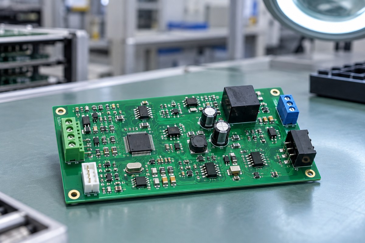
Single sided PCB assembly means that all mounted components are placed on one side of the finished circuit board. This describes the component population, not necessarily the number of copper layers inside the PCB. A board can have one copper layer and components on one side, but a multilayer PCB can also use single-sided assembly when all packages are mounted on the same surface.
That distinction matters because “single sided” can refer to three different features:
- A single sided PCB has one conductive copper layer.
- Single sided assembly places all components on one side of the board.
- Single-pass soldering describes a production route, but it does not automatically define the board’s copper-layer count or component layout.
Traditional single-layer boards often combine through-hole parts inserted from the component side with leads soldered on the copper side. An SMT design usually places both pads and components on the copper-patterned surface. Mixed technology can combine SMT and through-hole parts on one populated side, although the solder joints may be formed through different processes.
The practical benefit appears when the circuit is simple enough to remain accessible on one side. Fewer placement surfaces can simplify tooling, handling, visual inspection, repair, and process control. Once jumpers, awkward package orientations, thermal crowding, or excessive board area are needed to preserve that restriction, the single-sided format may no longer be the lower-cost solution.
How Are SMT and Through-Hole Components Placed on a Single Sided PCB?
SMT and through-hole components can share a single sided PCB, but their mounting and soldering paths are different. Surface-mount packages sit directly on pads. Through-hole parts pass through drilled holes, and their leads are soldered on the opposite surface. The placement plan must therefore consider component access, lead direction, solder contact, and the order of each operation.
For SMT-only assembly: solder paste is printed onto the pads, components are placed on the same surface, and the board passes through reflow. This is efficient for compact resistors, capacitors, ICs, and other packages that are suitable for automated placement.
For through-hole assembly: parts are inserted from the component side and soldered from the reverse side by wave soldering, selective soldering, or a controlled manual process. Connectors, transformers, relays, and mechanically loaded parts often use this method when their package or retention requirements make through-hole mounting appropriate.
For mixed assembly: SMT parts are usually placed and reflowed first. Through-hole parts are then inserted and soldered using a process compatible with the component bodies, spacing, and exposed SMT features. Pallets or selective soldering may be required when previously mounted parts must be protected from the solder wave.
Keeping all components on one side can make markings easier to read and service access more direct. However, the layout still needs adequate spacing around connectors, tall parts, polarized packages, test points, and soldering areas. A one-sided population only creates value if those features can be assembled without excessive manual correction or special handling.
How Does Single Sided PCB Assembly Move Through Production?
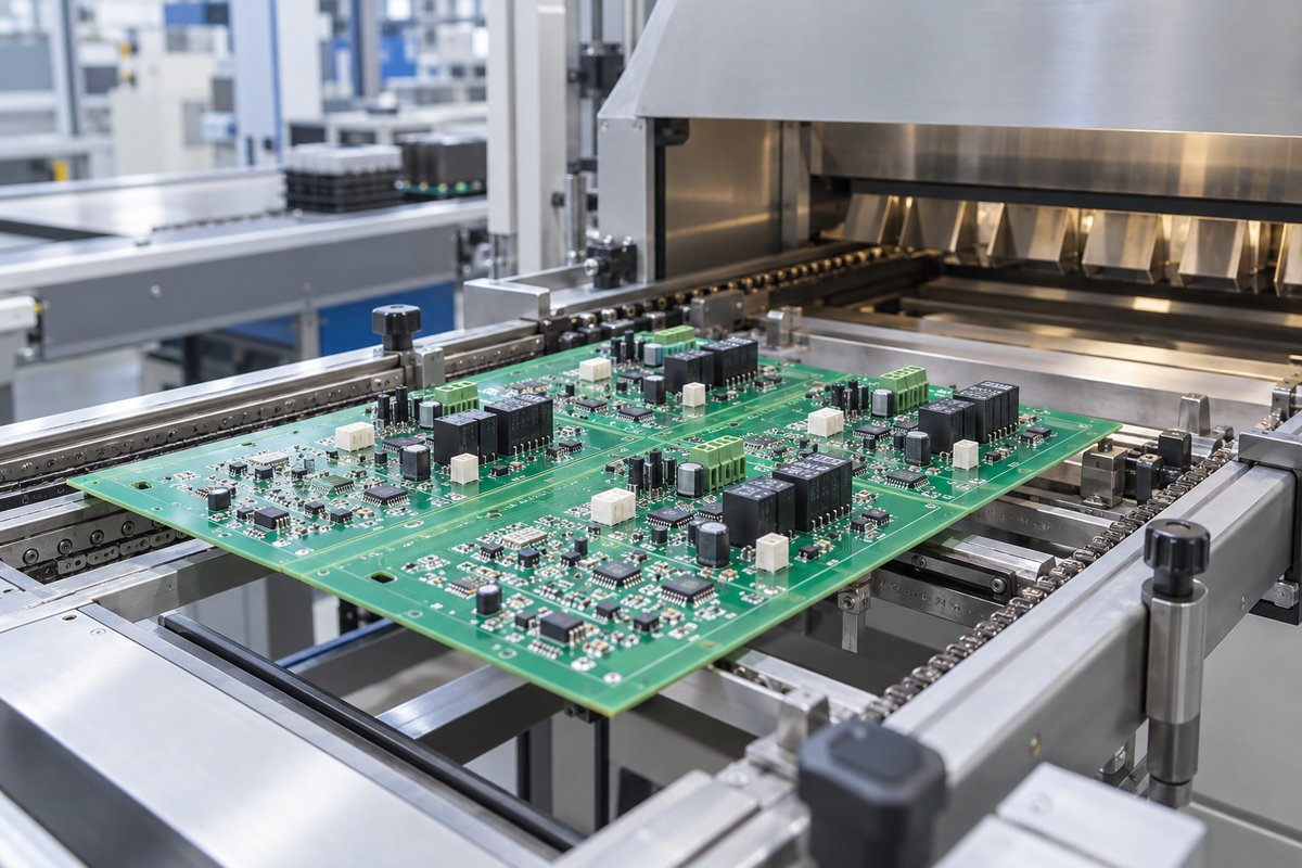
Single sided PCB assembly moves through production by matching the released board data and BOM to a controlled SMT, through-hole, or mixed-assembly route. A typical build follows this sequence:
- Data and BOM review: Gerber or ODB++ data, drill files, drawings, centroid data, BOM details, component orientations, and revision identifiers are checked for agreement.
- Bare-board fabrication and inspection: the PCB is built to the approved stackup, copper, solder-mask, surface-finish, outline, and hole requirements before assembly begins.
- Material preparation: component identity, package, value, quantity, moisture sensitivity, polarity, and approved substitutions are controlled against the released BOM.
- SMT processing where required: solder paste is printed, paste deposition is checked, components are placed, and the board is reflowed under an established thermal profile.
- Through-hole processing where required: leads are inserted, formed when permitted, and soldered by the selected wave, selective, or manual method.
- Cleaning, inspection, and testing: residues are managed according to the process specification, solder joints and component placement are inspected, and the agreed electrical tests are completed.
This route may be shorter than a two-sided assembly because the board does not require a second stencil print and placement cycle. It may also avoid the support, adhesive, or reflow considerations created by components on the underside. The actual saving depends on the component mix: a board dominated by manual through-hole work can still require substantial labor even though every part is on one side.
Stable repeat production depends on preserving the approved footprint geometry, solder volumes, component orientations, and process sequence. When a prototype uses hand-soldered substitutions or temporary jumpers, those exceptions should be resolved before the same board is treated as a production-ready single-sided assembly.
What Determines Single Sided PCB Assembly Cost?
Single sided PCB assembly cost is determined by the complete production route, not by component-side count alone. A one-sided population often costs less when it removes a second placement cycle, reduces fixtures and handling, and supports efficient panel processing. Those savings can disappear when the layout demands intensive manual insertion, unusual masking, selective soldering, rework, or a larger PCB.
The strongest cost drivers are:
- Component count and package mix: automated SMT placement is usually more scalable than repeated manual insertion, lead forming, or hand soldering.
- Board size and panel utilization: spreading a circuit over a larger one-sided board can reduce the number of units per panel and increase bare-board material cost.
- Assembly sequence: mixed SMT and through-hole builds require more operations than SMT-only boards, even when all components occupy one side.
- Tooling and soldering access: wave pallets, selective-solder fixtures, masking, or restricted nozzle access add setup and process time.
- Inspection and test coverage: AOI, X-ray where applicable, in-circuit testing, functional testing, programming, and custom fixtures affect non-recurring and per-unit cost.
- Volume and change frequency: prototypes absorb setup over few units, while stable repeat orders can distribute programming, stencil, tooling, and process-preparation costs more efficiently.
The lowest quoted board price is therefore not always the lowest finished PCBA cost. If a single-sided constraint increases board area, jumper count, hand work, or defect opportunities, a compact double-sided layout may produce a better total cost. Cost comparison should use the same quantity, test scope, sourcing responsibility, quality requirements, and delivery assumptions so that the two assembly options are evaluated on equal terms.
How Does Single Sided PCB Assembly Compare With Double Sided PCB Assembly?
Single sided PCB assembly usually offers a simpler production path, while double sided PCB assembly provides more placement area and routing freedom. The better option depends on whether the second populated surface removes more cost and risk than it adds.
| Production factor | Single sided assembly | Double sided assembly |
|---|---|---|
| Component placement | All components occupy one surface | Components are placed on both surfaces |
| Typical process flow | One SMT placement side, with optional THT operations | Two placement sequences may be required |
| Board area | May need more area for the same component count | Can reduce footprint by using both surfaces |
| Handling and tooling | Usually simpler | Requires control of the first-side components during second-side processing |
| Inspection and repair | Components are accessible from one side | Access and traceability must cover both sides |
| Best fit | Lower-density, cost-sensitive, serviceable products | Compact, dense, interface-rich, or space-constrained products |
A double-sided build does not automatically mean twice the assembly cost. Small passive components on the underside may allow a much smaller PCB, a shorter signal path, or a cleaner connector arrangement. Conversely, placing heavy or heat-sensitive parts on the second side can complicate reflow support and inspection.
The useful comparison is therefore process-specific. If all parts fit comfortably on one side with reliable solder access and acceptable board dimensions, single-sided assembly can keep production direct. If one-sided placement creates crowding, long routes, thermal concentration, too many jumpers, or difficult soldering, using both sides can make the finished PCBA easier to manufacture consistently.
Where Does Single Sided PCB Assembly Work Best—and Where Does It Fall Short?
Single sided PCB assembly works best in products with modest component density, uncomplicated interconnections, sufficient board area, and no strong need to minimize enclosure size. Common examples include simple power controls, indicator boards, appliance controls, relay boards, LED products, basic sensor interfaces, and low-complexity industrial electronics. The format is also useful when visible component identification and straightforward repair access matter.
Its limitations appear as the circuit becomes denser or more demanding. A one-sided component population can become restrictive when the product needs fine-pitch processors, large memory groups, many connectors, controlled-impedance interfaces, short high-current paths, extensive shielding, or concentrated thermal management. Forcing those functions onto one surface can enlarge the board or produce congested routing and uneven heat distribution.
Mechanical conditions matter as well. Tall components may conflict with the enclosure even if enough board area exists. Connectors may need fixed edge locations, displays or switches may have user-interface constraints, and heavy parts may require additional support. These factors can make a seemingly simple one-sided layout difficult to assemble or install.
The format is most successful when it follows the product’s real requirements rather than serving as an absolute design rule. Keeping one assembly side is worthwhile when it simplifies production without creating penalties elsewhere. When density, thermal performance, signal behavior, or enclosure limits become dominant, a double-sided or multilayer solution may deliver a more reliable and economical result.
How Are Single Sided PCB Assemblies Inspected and Tested?
Inspection and testing should verify both the general assembly quality and the features that are critical to the product’s function. Because components are concentrated on one side, visual access may be easier, but one-sided placement does not eliminate defects such as wrong parts, polarity errors, insufficient solder, bridging, lifted leads, contamination, or damaged through-hole barrels.
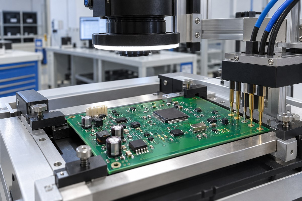
The inspection route can include:
- Incoming and bare-board checks for dimensions, finish, solder mask, markings, holes, and electrical continuity.
- Solder-paste inspection for SMT builds where paste volume and alignment influence joint formation.
- Automated optical inspection for component presence, orientation, polarity, placement, and visible solder conditions.
- Visual inspection for through-hole fill, lead protrusion, solder bridges, flux residues, mechanical damage, and workmanship details not fully covered by AOI.
- X-ray inspection when hidden joints or package geometry justify it; X-ray is not required merely because the assembly is single sided.
- Electrical testing such as continuity, shorts testing, in-circuit testing, programming, or functional testing according to the agreed product requirements.
Inspection must match the technology on the board. A through-hole connector needs different acceptance evidence from a small SMT resistor, while a programmed controller requires more than a visual solder-joint check. Clear test limits, fixtures, firmware versions, and pass/fail conditions allow the finished units to be evaluated consistently across production lots.
FAQs About Single Sided PCB Assembly
Is a single sided PCB the same as single sided PCB assembly?
No. A single sided PCB has one conductive copper layer, while single sided PCB assembly means all mounted components occupy one side. A multilayer board can still use a one-sided component population.
Can SMT and through-hole parts be assembled on the same side?
Yes. SMT and through-hole parts can share one component side, but they normally require different placement and soldering operations. Their spacing and process order must allow each operation to be completed without damaging previously mounted parts.
Is single sided PCB assembly always cheaper?
No. It is often economical when it eliminates second-side processing without increasing board area or manual work. A double-sided assembly may cost less overall if it reduces PCB size, jumpers, routing difficulty, special tooling, or rework.
Can a multilayer PCB use single-sided component assembly?
Yes. Copper-layer count and component-side count are separate choices. A multilayer PCB may keep every component on one surface to simplify assembly or meet mechanical requirements.
What files are needed to quote a single sided PCB assembly?
A usable quotation package normally includes PCB fabrication data, a fabrication drawing or stackup requirements, the BOM, centroid or pick-and-place data for SMT parts, assembly drawings, polarity and revision information, and the required inspection, programming, and test scope.
Single sided PCB assembly is most valuable when one populated surface simplifies production without forcing extra board area, jumpers, or manual operations. EBest Circuit can review customer-released PCB and assembly data, manufacture the bare boards, source approved components, complete SMT and through-hole assembly, and perform agreed inspection and testing. To discuss a prototype or repeat-production build, contact sales@bestpcbs.com.
You may also like
Tags: Single Sided PCB Assembly, SMT assembly, through-hole assembly