PCB manufacturing PCB manufacturing
Home > Blog

Schematic Symbols

How to Read a Circuit Diagram Schematic: Step-by-Step PCB Guide
Wednesday, July 29th, 2026

How to read a circuit diagram schematic begins with one principle: a schematic shows electrical relationships, not the physical positions of parts on a PCB. Start by identifying the power source and ground, divide the drawing into functional blocks, follow named nets and signal paths, and then verify component references, values, pin numbers, and page connections. This method works more reliably than trying to read every line from the upper-left corner to the lower-right corner.

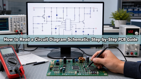
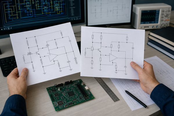
How to read a circuit diagram schematic on an electronics engineering workstation

What Does a Circuit Diagram Schematic Show?

A circuit diagram schematic shows which component pins are electrically connected and how power, signals, and control functions move through a design. Symbols stand for components, lines and labels identify electrical nets, and reference designators link each symbol to controlled design data.

The drawing is logical rather than physical. Two symbols placed next to each other may be far apart on the finished board. Two points on different pages may be electrically connected by the same net label. A schematic also does not define trace width, copper layer, via structure, component rotation, or exact placement unless that information is added separately.

This distinction prevents a common error: treating the schematic as a map of the PCB. The schematic explains what must connect and why. The PCB layout determines where components, pads, copper traces, planes, and vias are physically implemented.

How Do You Read Schematics Step by Step?

Read schematics by moving from overall purpose to individual connections. The following sequence keeps a complex page manageable:

  1. Confirm the drawing type. Determine whether the file is an electronic schematic, wiring diagram, block diagram, or PCB layout.
  2. Read the title block and notes. Check the sheet name, revision, page references, voltage domains, and drawing conventions.
  3. Locate power entry and ground. Identify input connectors, protection, regulation, power rails, and return references.
  4. Divide the design into functional blocks. Typical blocks include input protection, power conversion, sensors, analog conditioning, processing, communications, and output drivers.
  5. Choose one signal path. Follow it from its source through each stage to its destination rather than jumping between unrelated nets.
  6. Read symbols together with their fields. Check reference designators, values, part numbers, pin names, and polarity.
  7. Follow named nets and page links. A label can connect distant points without a continuous drawn wire.
  8. Cross-check supporting files. Compare the schematic with the BOM, datasheets, PCB layout, and assembly information.

Repeat the process for each power rail, interface, and functional signal. A first pass establishes structure; later passes resolve component-level behavior.

Which Circuit Symbols Should You Recognize First?

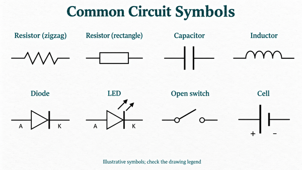
Begin with the symbols that appear in nearly every electronic schematic: power sources, ground, resistors, capacitors, inductors, diodes, transistors, integrated circuits, connectors, switches, and test points. You do not need to memorize every device variant before reading a basic circuit.

Symbol group What it tells you What still needs verification
Power and ground Supply rails, references, returns, chassis, or earth connections Voltage, current limit, sequencing, and whether grounds are intentionally separated
R, C, and L Resistance, capacitance, inductance, filtering, timing, biasing, or energy storage Value, tolerance, rating, package, and frequency behavior
Diodes and transistors Polarity, switching, rectification, clamping, amplification, or drive functions Exact device, pinout, voltage, current, and thermal limits
IC blocks Functional pins and logical relationships Datasheet pin functions, supply pins, package mapping, and unused-pin requirements
Connectors Signals entering or leaving the circuit Pin numbering, mating view, cable orientation, and external voltage levels

Symbol appearance can vary between IEC and ANSI/IEEE conventions. The existing electrical symbols and electronic symbols chart covers these variants in more detail. Always interpret a symbol with its designator and surrounding circuit rather than by shape alone.

How Do Reference Designators, Values, and Pin Numbers Work?

A reference designator identifies one specific component instance. The letter indicates the component class and the number distinguishes it from other parts of the same class. Common examples include R for resistor, C for capacitor, L for inductor, D for diode, Q for transistor, U for integrated circuit, J for connector, and TP for test point.

The nearby value field explains what that instance is. `R12 10 kΩ` identifies a particular 10-kilohm resistor; `C7 100 nF` identifies a particular capacitor. An IC may show a device name instead of a simple numeric value. Do not assume the field contains every required rating. Voltage rating, tolerance, dielectric, package, manufacturer part number, and approved alternatives may reside in the BOM or component database.

Pin names describe function, while pin numbers connect the logical symbol to the physical package. An IC symbol may group power pins, analog pins, and digital pins for readability, so the displayed order often differs from the package’s clockwise pin order. Verify the symbol-to-footprint pin mapping against the datasheet before using the schematic to diagnose or manufacture a board.

How Do Wires, Junctions, Nets, and Labels Work?

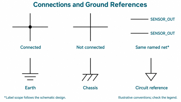
A net is a set of electrically connected pins and conductors. A drawn line normally indicates a connection, while a junction dot marks multiple lines that share the same node. Crossing lines without a dot usually do not connect, although older drawing conventions may use a bridge or other notation. Check the drawing legend when the convention is unclear.

Net labels connect points by name. Every point labeled `3V3` belongs to the same 3.3 V network unless the design tool or hierarchy defines a narrower scope. Labels such as `SCL`, `SDA`, `RESET`, `USB_D+`, or `MOTOR_EN` are often more useful than the visual line because they state the signal’s role.

Hierarchical labels and off-page connectors move signals between sheets. A continuation marker should provide a page, block, port, or net name that can be followed. When a line seems to end without explanation, look for a label before assuming the circuit is incomplete.

How Should You Find Power and Ground?

Start at the power connector, battery, USB input, or other supply source. Follow the path through fuses, reverse-polarity protection, transient suppressors, filters, regulators, and current-sense elements. Record each resulting rail, such as 12 V, 5 V, 3.3 V, 1.8 V, or an isolated supply.

Next, identify the ground references. A design may contain digital ground, analog ground, power ground, chassis ground, protective earth, or an isolated secondary return. They are not automatically interchangeable. Look for explicit connection points, net ties, ferrites, resistors, capacitors, or isolation barriers that define how the references relate.

Power symbols can hide long connections and may also hide IC supply pins in some libraries. Check the component unit and datasheet if an IC appears to have no power pins. A signal can only be interpreted correctly after its voltage domain and reference are known.

How Do You Trace Signal Flow Through a Schematic?

Choose one input and follow it through each functional stage. A sensor signal, for example, may pass through protection, filtering, biasing, amplification, analog-to-digital conversion, digital processing, and an output driver. Read one chain completely before moving to another.

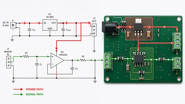
Power path and signal path traced from an electronic schematic to a PCB

Signal flow is not always left to right. Feedback paths return from an output to an earlier stage; bidirectional buses carry information both ways; differential pairs use two complementary nets; and power-control signals may cross several voltage domains. Arrows, pin names, datasheet block diagrams, and interface standards help determine direction.

At each stage, ask what changes: voltage level, current capability, frequency content, logic state, impedance, or isolation. This turns a line-following exercise into an explanation of circuit behavior.

How Do You Divide a Complex Schematic into Functional Blocks?

Functional blocks reduce a large schematic into smaller circuits with clear inputs and outputs. Begin with obvious anchors such as connectors, regulators, microcontrollers, communication transceivers, sensors, and power switches. Then group the surrounding passive components according to the device they support.

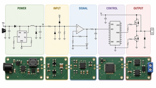
Electronic schematic divided into power input signal control and output blocks

A practical block sequence might be:

  • power entry, protection, conversion, and distribution;
  • external inputs and interface protection;
  • analog filtering, sensing, or amplification;
  • processor, memory, clock, and reset;
  • communications and level translation;
  • output drivers, loads, and connectors.

After identifying the blocks, trace the nets that cross their boundaries. These interfaces reveal the system architecture more quickly than reading every local bypass capacitor or pull resistor first.

How Do You Read Multi-Sheet and Hierarchical Schematics?

Multi-sheet designs use hierarchy to prevent one page from becoming unreadable. A top sheet may show major blocks as sheet symbols, while lower-level sheets contain their detailed circuits. Ports on the parent sheet must correspond to hierarchical labels on the child sheet.

Use the sheet index, page references, and net names as navigation tools. Global labels may connect all sheets, while local labels may apply only inside one sheet or hierarchy level. The exact scope depends on the EDA system and project settings.

Also check repeated channels. One amplifier or sensor block may be instantiated several times with different reference designators. Confirm which channel you are tracing and whether shared power, reference, or control nets affect every instance.

How Is a Schematic Different from a Wiring Diagram and PCB Layout?

A schematic emphasizes electrical function. A wiring diagram emphasizes physical terminals, wire colors, harness routes, and installation connections. A PCB layout implements the schematic as footprints, placement, copper, vias, planes, mechanical outlines, and fabrication layers.

Document Main question answered Typical information
Schematic What is electrically connected and how should the circuit work? Symbols, pins, nets, values, labels, and functional relationships
Wiring diagram How are physical devices or terminals wired together? Wire numbers, colors, connectors, terminal blocks, routes, and harness details
PCB layout How is the electronic circuit physically built on the board? Footprints, placement, traces, vias, planes, stack-up, and mechanical constraints

Use the correct document for the task. A schematic can reveal that two pins share a net, but it cannot show whether a copper trace is damaged. A PCB layout can show where the trace runs, but it may not explain the intended signal behavior as clearly as the schematic.

How Do You Read a Simple LED Circuit Step by Step?

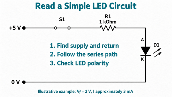
Consider a DC source connected to a current-limiting resistor, an LED, and ground. First identify the supply voltage and its return. Next check LED polarity: conventional current enters the anode and leaves the cathode. Then read the resistor value and verify that it limits current to an appropriate level for the selected LED and supply.

Trace the closed path: positive supply → resistor → LED → ground or negative return. If a transistor controls the LED, separate the load path from the control path. The transistor may switch LED current while a GPIO drives its base or gate through another resistor. A pull-down or pull-up sets a known state when the controller output is inactive.

This example demonstrates the full method on a small circuit: identify power, recognize symbols, read values and polarity, trace the active path, and distinguish control from load current.

Which Schematic Reading Mistakes Can Cause PCB Problems?

The most consequential errors are usually connection or mapping errors rather than unfamiliar symbols.

  • Missing a junction: a connected node is treated as two separate nets, or crossing lines are incorrectly joined.
  • Ignoring polarity: a diode, LED, electrolytic capacitor, or polarized connector is interpreted backward.
  • Confusing pin names and numbers: the logical function is assigned to the wrong package pad.
  • Overlooking global labels: distant points on the same rail are treated as unrelated.
  • Assuming ground symbols are identical: isolated, chassis, analog, and power returns are joined incorrectly.
  • Reading the symbol without the datasheet: device-specific pin behavior, ratings, or unused-pin rules are missed.
  • Assuming schematic position equals PCB position: troubleshooting begins in the wrong physical area.

Each interpretation should be checked against the design revision being used. A correct reading of an obsolete schematic can still lead to an incorrect conclusion about the current board.

How Do You Compare a Schematic with the BOM and PCB Layout?

Use the reference designator as the common key. The schematic identifies the function and connections of `U1`; the BOM identifies its approved part and package; the PCB layout identifies its physical footprint, orientation, and copper connections.

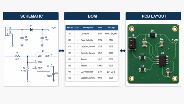
Cross-checking reference designators between schematic BOM and PCB layout

Check that every populated schematic reference has a corresponding BOM entry and footprint. Verify that symbol pin numbers match footprint pad numbers. Confirm polarized footprints, connector views, pin 1 markers, and multi-unit components. For net checks, select a schematic net and verify that the same net connects the intended pads in the layout.

This cross-check is especially important before PCB assembly, because the schematic, BOM, placement data, and board layout must describe the same revision. EBest Circuit (Best Technology) uses engineering review to identify inconsistent component references, polarity information, footprint assignments, and production data before assembly begins.

FAQ About Reading Circuit Diagram Schematics

Can ChatGPT read electrical schematics?

AI can help identify common symbols, summarize functional blocks, and explain likely signal paths when the schematic is clear. It can still misread small labels, junction dots, pin numbers, or device-specific behavior. Verify every conclusion against the original high-resolution drawing, datasheets, netlist, and controlled design files.

How hard is it to read schematics?

Basic schematics become manageable after learning common symbols, nets, designators, power references, and a consistent reading sequence. Complex mixed-signal, RF, power, or multi-sheet designs require more circuit knowledge and careful datasheet review.

Do you read every schematic from left to right?

No. Many schematics are arranged approximately from input to output, but feedback, power distribution, buses, and hierarchical connections break that pattern. Start with functional blocks and follow one named path at a time.

What does a dot on crossing schematic lines mean?

A dot normally indicates an electrical junction. Crossing lines without a dot normally do not connect, but older drawings may use different conventions. Check the legend and nearby examples before deciding.

Why do IC pins appear out of numerical order?

Schematic symbols often group pins by function to improve readability. The physical package still follows its numbered pad arrangement, so the symbol pin numbers must be checked against the datasheet and footprint.

What should you check first on an unfamiliar schematic?

Check the title, revision, sheet structure, power inputs, ground references, main connectors, and major ICs. These elements reveal the circuit’s purpose and provide stable starting points for tracing individual signals.

Conclusion

How to read a circuit diagram schematic becomes much easier when the drawing is treated as a network of functional blocks rather than a page of unrelated symbols. Find power and ground, follow one signal path at a time, use net labels and page references, and verify every designator, value, pin, and footprint against the supporting files.

EBest Circuit (Best Technology) supports PCB fabrication and PCBA assembly with engineering review of schematics, BOMs, Gerber or ODB++ data, component placement, polarity, footprints, and manufacturing consistency. For PCB or PCBA support, contact sales@bestpcbs.com.

You may also like

Electrical Symbols & Electronic Symbols: Complete Circuit Chart
Wednesday, July 22nd, 2026

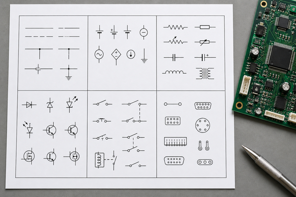
Electrical symbols & electronic symbols are the graphic language used to show components, connections, power rails, control functions, and signal flow in a schematic. This guide explains the most common electrical symbols and electronic symbols, how they are grouped, how IEC and ANSI/IEEE conventions can differ, and how a schematic symbol relates to a physical PCB footprint and board marking.

Electrical symbols and electronic symbols shown with a PCB schematic

What Are the Basic Electrical Symbols?

Basic electrical symbols represent conductors, connection points, power sources, grounds, switches, protective devices, loads, and measuring instruments. Basic electronic symbols extend that vocabulary to resistors, capacitors, inductors, diodes, transistors, integrated circuits, sensors, and signal-processing blocks.

A symbol communicates function, not physical appearance. A resistor may be drawn as a rectangle or a zigzag line, but neither shape predicts whether the installed part is an axial lead resistor, a 0402 chip, or a power resistor. The schematic must therefore be read together with its reference designators, values, net labels, and component library data.

  • Graphic symbol: identifies the electrical function of a component or connection.
  • Reference designator: gives each instance a unique identifier, such as R12, C7, D3, Q2, or U5.
  • Value or part field: states a resistance, capacitance, device type, or manufacturer part number.
  • Net label: names a connection such as 3V3, GND, USB_D+, or RESET.
  • Pin number: links each schematic terminal to a package pad or connector contact.

What Is the Difference Between Electrical Symbols and Electronic Symbols?

Electrical symbols often describe power distribution, electromechanical control, protection, wiring, motors, transformers, switches, and grounding. Electronic symbols more often describe low-voltage signal circuits, semiconductor devices, logic functions, sensors, and integrated circuits. The categories overlap because a PCB schematic can contain power inputs, fuses, relays, resistors, processors, and connectors on the same sheet.

The drawing type matters more than the label. A wiring diagram emphasizes physical terminals, harnesses, wire colors, and installation routes. A schematic emphasizes functional connectivity and signal flow. A PCB layout then converts that logical network into pads, copper traces, vias, planes, and component placement. Readers who need a broader method for following sheets and functional blocks can use this guide to understand circuit diagrams.

Electrical Symbols Chart: Common Circuit Symbols and Meanings

This electrical symbols chart groups common circuit diagram symbols and electrical diagram symbols by function. The table focuses on what each symbol tells the reader and what additional data must be checked before treating it as a physical component.

Common circuit symbol categories on an engineering schematic
Category Common examples Typical designators What the symbol does not define
Conductors Wire, bus, junction, no-connect Net names Trace width, layer, copper weight, or cable gauge
Power and reference Battery, DC source, AC source, earth, chassis, signal ground BT, V, GND, PE Current capacity, isolation, or return-path implementation
Passive components Resistor, capacitor, inductor, transformer R, C, L, T Package, tolerance, voltage rating, or power rating
Semiconductors Diode, LED, transistor, MOSFET, optocoupler D, LED, Q, U Pinout, package orientation, or thermal pad geometry
Control and protection Switch, relay, fuse, circuit breaker SW, K, F, CB Contact rating, actuation force, or fault interrupt rating
Integrated circuits Op-amp, logic gate, MCU, regulator, memory U, IC Exact package, exposed pad, or unused-pin treatment
Interfaces Connector, test point, terminal, antenna J, P, TP, AE Mating part, keying, contact plating, or mechanical keep-out
Measurement and output Ammeter, voltmeter, lamp, speaker, buzzer M, DS, LS, BZ Range, drive circuit, acoustic output, or mounting method

Reference-designator prefixes vary between companies and standards. The component library, project convention, and approved parts list remain authoritative for a specific design.

What Is the Symbol for Electric Wire?

An electric wire or schematic connection is normally shown as a line between terminals. A filled junction dot indicates that conductors are electrically connected. Crossing lines without a junction dot are commonly interpreted as not connected, although older drawings may use a small bridge or crossover. Because conventions vary, ambiguous crossings should be replaced with explicit junctions or net labels.

A schematic line does not automatically mean a single physical wire or one PCB trace. It may represent a copper trace, a plane connection, a harness conductor, a cable shield, a differential pair, or a named net repeated across several sheets. Bus lines collect related signals, while off-page connectors and hierarchical ports carry nets between sheets. Net names and pin numbers are therefore as important as the line itself.

What Do Power, Ground, and Source Symbols Mean?

Power-source symbols identify batteries, DC rails, AC sources, and controlled sources. A battery is conventionally represented by paired long and short plates, while a single-cell symbol uses one plate pair. In electronic schematics, named power ports such as VCC, VDD, 5V, or 3V3 often replace a drawn source on every sheet.

Ground symbols require careful interpretation. Protective earth is associated with safety bonding. Chassis ground refers to the equipment enclosure or shield structure. Signal ground is a circuit reference and may be separated into analog, digital, power, or isolated domains. Using one generic ground symbol everywhere can hide intentional isolation or create an unintended return path when the design is transferred to the PCB.

What Do Resistor, Capacitor, and Inductor Symbols Mean?

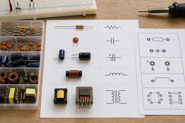
Resistors are shown with a rectangular or zigzag convention, and a diagonal arrow identifies an adjustable element such as a variable resistor or potentiometer. Capacitors use two electrodes; polarized versions include polarity information or a differentiated plate. Inductors use a coil convention, while coupled coils indicate a transformer or common-mode choke.

Passive component symbols compared with PCB components

The symbol alone is insufficient for component selection. R47 still needs a resistance, tolerance, power rating, voltage rating, temperature coefficient, and package. C18 may need capacitance, dielectric, working voltage, polarity, ESR, and bias behavior. L3 may require inductance, saturation current, DC resistance, shielding, and self-resonant frequency. For a focused explanation of coil notation and variants, see the inductor symbol guide.

What Do Diode, LED, Transistor, and IC Symbols Mean?

Semiconductor symbols communicate polarity, control terminals, or internal function. Diodes identify anode and cathode orientation; LED symbols add outward light arrows, while photodiodes reverse the arrow direction to indicate incident light. Zener, Schottky, TVS, and varactor symbols add distinguishing features that must match the intended device family.

Transistor symbols distinguish BJT, JFET, and MOSFET structures and show the terminals needed to interpret bias and current paths. Do not infer a package pinout from the symbol position. A gate drawn on the left does not guarantee that pad 1 is the gate, and two transistors with the same function may use different package pin numbering. The transistor symbol and pinout guide explains this distinction in more detail.

Integrated circuits are commonly drawn as functional blocks with named pins. A multi-unit op-amp may place amplifier sections and power pins in separate schematic units. Microcontrollers and FPGAs may split hundreds of pins across several blocks. Designers must confirm that every unit is present, power pins are connected, unused inputs have a defined state, and hidden pins have not created accidental nets.

For LED-specific polarity and board checks, use the LED symbol guide. These device-level pages carry details that would otherwise make a general symbol chart repetitive.

What Do Switch, Relay, Fuse, and Connector Symbols Mean?

Switch symbols show contact count, pole and throw arrangement, and normal state. SPST, SPDT, DPST, and DPDT describe how many circuits are controlled and how many output paths each pole can select. Momentary pushbuttons are also marked as normally open or normally closed. The schematic normal state is usually the unactuated, de-energized state unless the drawing states otherwise.

A relay symbol separates the coil from its contacts, and matching designators show that they belong to the same device. Fuse and circuit-breaker symbols indicate protection but not the current-time curve, breaking capacity, or voltage rating. Connector symbols show contacts and numbering; the mating face, cable side, board side, and view direction must be defined to prevent mirrored pin assignments.

How to Interpret Electrical Symbols?

Read a schematic in layers instead of decoding every mark in isolation. First identify the power inputs, ground domains, major functional blocks, and connectors. Then follow named nets from input to output. Within each block, combine the symbol, reference designator, value, pin names, and surrounding components to infer function.

  1. Read the title block, revision, sheet hierarchy, and symbol legend.
  2. Locate power rails, ground domains, isolation barriers, and protection devices.
  3. Identify functional blocks such as power conversion, sensing, processing, memory, and communication.
  4. Follow net labels and off-page references instead of relying only on line proximity.
  5. Check component values, polarity marks, pin names, and reference designators.
  6. Compare the symbol-to-footprint pin mapping before using the drawing for PCB layout or assembly review.
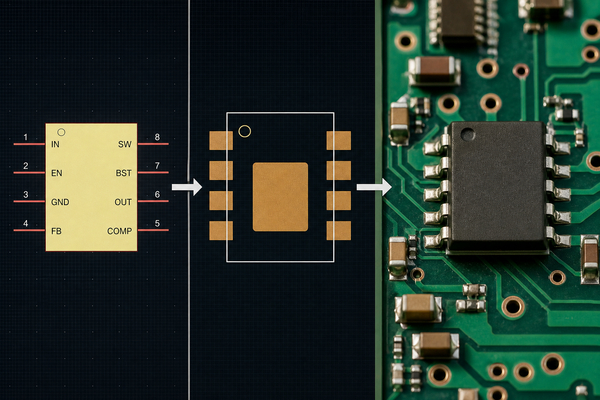
Do not assume signal direction solely from left-to-right placement. Bidirectional buses, feedback loops, power returns, and open-drain nets may flow differently. The symbol tells you the device type; the surrounding network tells you how it is being used.

How Do IEC and ANSI/IEEE Symbols Differ?

IEC 60617 is the international database for graphical symbols used in electrotechnical diagrams. It organizes symbols for conductors, passive components, semiconductors, power conversion, switchgear, measurement, telecommunications, logic, and related areas. The database is the appropriate reference when a project specifies IEC conventions.

Engineer comparing IEC and ANSI schematic symbol conventions

ANSI/IEEE drawings may use different graphical traditions, including the familiar zigzag resistor convention, while IEC drawings commonly use a rectangular resistor. IEEE/ANSI 315 is still encountered in legacy documentation, but IEEE marks the 1975 standard as inactive-reserved. A current project should state its governing standard and library convention rather than assuming every drawing uses one universal shape set.

Differences are not limited to appearance. Contact states, terminal markings, logic notation, ground types, and reference designations can also vary by industry or company practice. A legend is especially useful when a drawing combines imported libraries or older subsystems.

How Do Schematic Symbols Map to PCB Footprints and Board Markings?

A schematic symbol is a logical object. A PCB footprint is a physical land pattern with pads, courtyard, assembly outline, and often a 3D model. The symbol pins map to footprint pads by number or name. That mapping must match the component datasheet; otherwise a perfectly routed PCB can still connect the wrong physical leads.

Schematic symbol mapped to a PCB footprint and board markings

Reference designators such as R12 and U3 identify component instances. They are not symbols and do not specify values. PCB silkscreen markings may include the designator, pin-1 mark, polarity mark, connector orientation, or test label, but limited board space often means only a subset is printed. The circuit board markings guide explains how these physical markings differ from schematic notation.

Physical identification also depends on package codes and placement context. The PCB components identification guide and the overview of surface mount electronic components help connect schematic intent to real components on an assembled board.

What Symbol Errors Cause Schematic and PCB Problems?

The most damaging errors usually occur at the boundaries between the symbol, library data, and physical implementation.

  • Wrong pin-to-pad mapping: the symbol looks correct, but gate, source, drain, collector, emitter, or connector pins map to the wrong pads.
  • Polarity ambiguity: diode, LED, electrolytic capacitor, battery, or IC pin-1 orientation is not carried consistently into the footprint and silkscreen.
  • Incorrect normal state: relay or switch contacts are interpreted as energized instead of de-energized.
  • Hidden power pins: a library connects power pins implicitly to a global net that is inappropriate for the design.
  • Duplicate or missing designators: the BOM and placement data cannot uniquely identify every component.
  • Unit or prefix errors: 1 mF, 1 uF, and 1 nF are confused, or decimal separators are misread.
  • Ambiguous wire crossings: junction dots are missing or a bridge convention is interpreted incorrectly.
  • Outdated library revisions: the schematic symbol, footprint, and approved part no longer describe the same package revision.

A practical review checks the symbol and footprint as a pair, compares pad numbering against the component datasheet, runs electrical-rule and design-rule checks, and confirms critical polarity and connector orientation in the assembly drawing. EBest Circuit (Best Technology) can support PCB design, fabrication, component sourcing, and PCBA when a project needs the schematic, layout, and production data reviewed as one connected dataset.

FAQ About Electrical and Electronic Symbols

What Are the Main Circuit Symbols?

The main groups are wires and junctions, power and ground, resistors, capacitors, inductors, diodes, transistors, integrated circuits, switches, relays, protection devices, connectors, sensors, and output devices. The exact symbol set depends on the drawing standard and circuit type.

What Is the Electricity Symbol?

There is no single schematic symbol that represents all electricity. Voltage, current, AC, DC, power, earth, and electrical hazards use different notations or equipment symbols. The drawing context determines which one is correct.

What Is the Symbol of a Resistor?

A fixed resistor is commonly shown as a rectangle under IEC practice or as a zigzag line in many ANSI-style and legacy drawings. The reference designator is normally R followed by a number.

What Are the On and Off Symbols?

On and off contact states are shown by the switch or relay contact position in its defined normal state. Equipment controls may also use the IEC power symbols I for on and O for off, but those equipment markings are not substitutes for a full schematic contact symbol.

What Is a Circuit Diagram?

A circuit diagram is a graphical representation of components and their electrical connections. A schematic prioritizes logical function, while a wiring or layout diagram emphasizes physical implementation.

What Is Circuit Notation?

Circuit notation is the combined system of graphic symbols, reference designators, values, net names, pin labels, and annotations used to describe a circuit consistently.

Can One Schematic Symbol Use Different PCB Footprints?

Yes. The same logical device may be available in several packages, but each footprint must have the correct pad geometry and pin mapping for the selected manufacturer part number. Footprints are not interchangeable merely because the schematic symbol is the same.

Conclusion

Accurate use of electrical symbols & electronic symbols makes a schematic readable, but production accuracy depends on more than recognizing shapes. Reference designators, net names, pin numbers, footprint mapping, polarity, and library revisions must remain consistent from schematic capture through PCB layout and assembly.

For support with PCB design, fabrication, component sourcing, or PCBA, contact EBest Circuit (Best Technology) at sales@bestpcbs.com.

You may also like

Switch SPDT Symbol: Meaning, Diagram & How to Read It
Thursday, May 28th, 2026

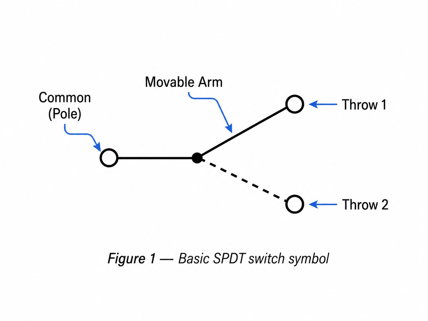
The switch SPDT symbol appears in almost every schematic that routes a signal between two destinations. It looks simple—one input arm pointing at two contacts—but reading it correctly tells you exactly how current flows through the circuit. This guide explains what the symbol means, how to read it, the IEC vs ANSI versions, and how to draw it yourself.

Figure 1: The basic Switch SPDT Symbol— one common (pole) terminal and two throw terminals.

What Is a SPDT Switch? (Single Pole, Double Throw Explained)

SPDT stands for Single Pole, Double Throw. In plain terms:

  • Single pole → one common input terminal (the “pole”).
  • Double throw → that input can connect to one of two output terminals.

So a SPDT switch has three terminals and acts as a changeover (or selector): it sends the common line to output A or output B, but never both at once. In British English, a SPDT used to control one light from two locations is called a two-way switch.

What Is the Symbol for a SPDT Switch?

The SPDT switch symbol is a single line (the moving contact) that pivots from one common terminal toward two separate contacts. The common terminal is the pole; the two contacts are the throws. The position of the arm shows which throw the pole is connected to.

You’ll also see it called a SPDT schematic symbol or SPDT circuit symbol—they all refer to the same thing.

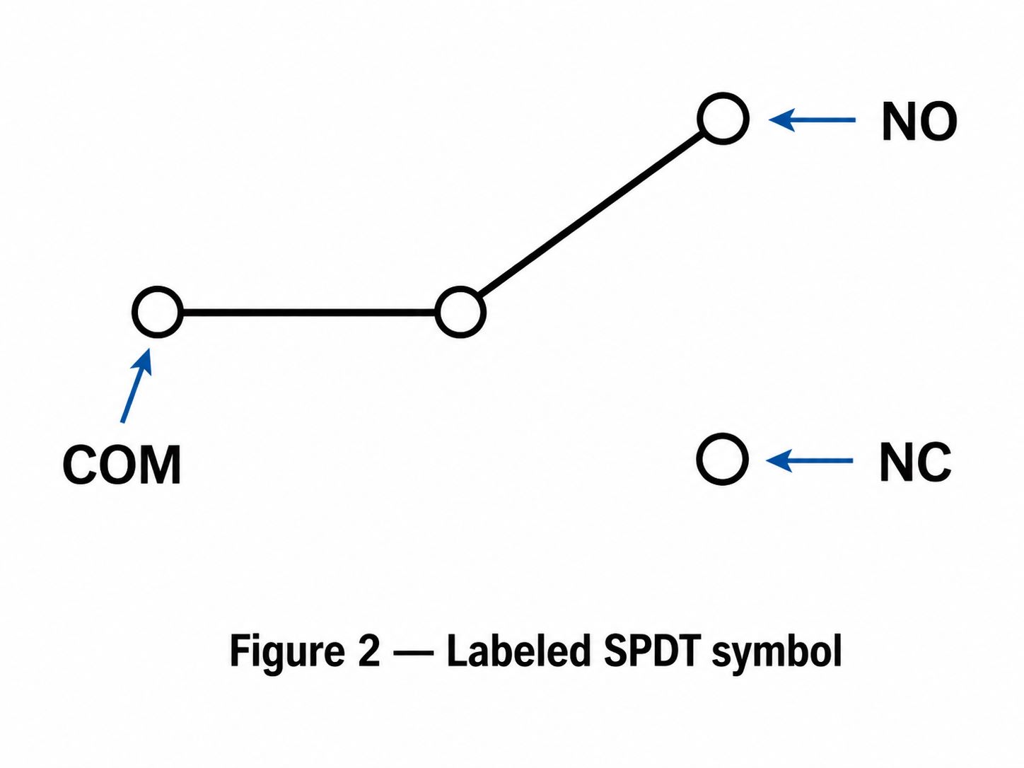
Figure 2: A labeled SPDT switch symbol showing the COM, NC, and NO terminals.

How to Read a SPDT Switch Symbol: The Pole and Two Throw Terminals

Read it in three steps:

  1. Find the common terminal (pole). It’s the single terminal the moving arm starts from—usually drawn as a dot or short line. This is your input.
  2. Find the two throw terminals. These are the two contacts the arm can reach. They’re your two possible outputs.
  3. Look at where the arm points. The arm shows the switch’s current state—connected to the upper throw or the lower throw.

The three terminals are commonly labeled:

  • COM — the common (pole)
  • NC — normally closed (connected to COM when the switch is at rest)
  • NO — normally open (connects to COM when the switch is actuated)

A SPDT is break-before-make by default: the arm leaves one throw before touching the other, so the two outputs are never shorted together.

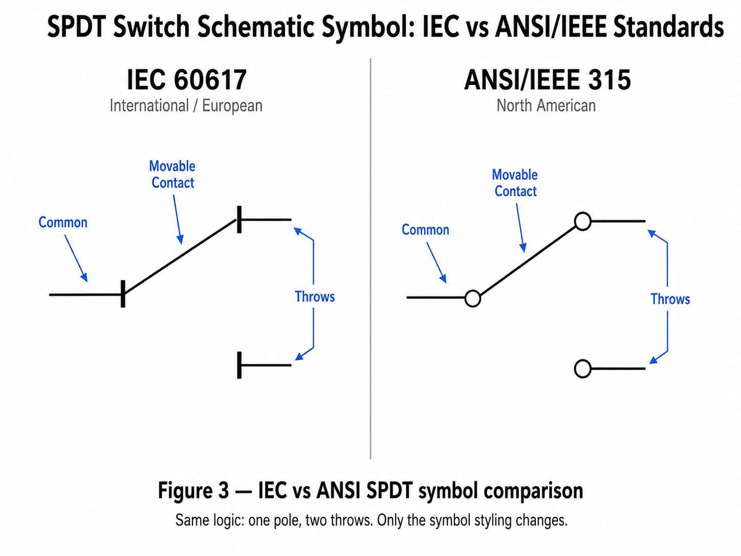
SPDT Switch Schematic Symbol: IEC vs ANSI/IEEE Standards

The SPDT symbol is nearly universal, but two standards govern the fine details:

  • IEC 60617 (international / European): draws the contacts as short bars or open marks, with a clean pivoting line for the moving contact.
  • ANSI/IEEE 315 (North American): very similar, typically with small open circles or dots for the contact points.

In both standards the logic is identical—one pole, two throws—so a schematic is readable either way. The differences are cosmetic: the shape of the contact points and the angle of the actuator line.

Figure 3: The SPDT switch symbol in IEC 60617 and ANSI/IEEE 315 styles.

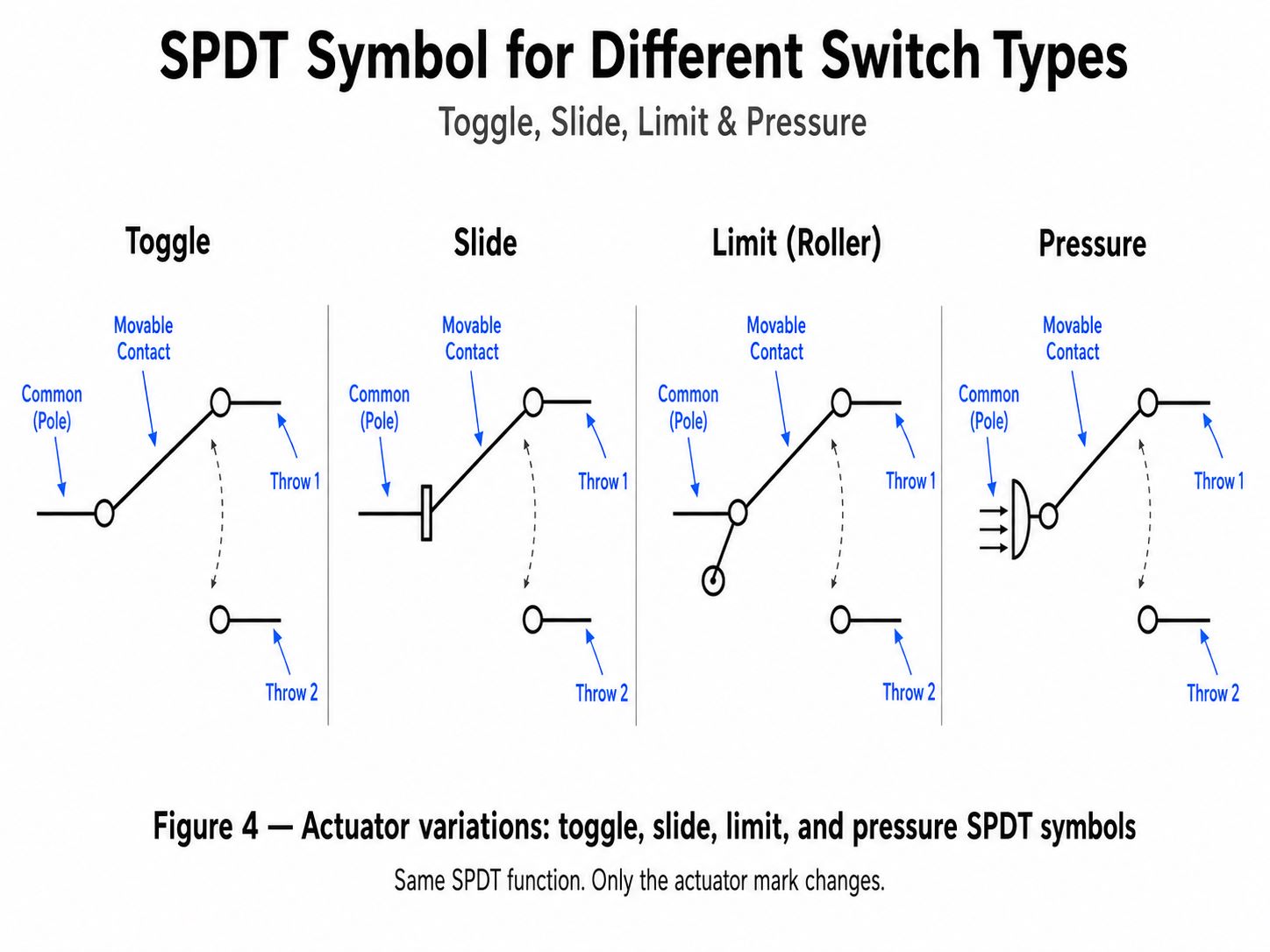
SPDT Symbol for Different Switch Types: Toggle, Slide, Limit & Pressure

The same SPDT symbol is used no matter the physical switch, because the symbol describes the function (one pole, two throws), not the actuator. The actuator may be shown with an extra mark:

  • SPDT toggle switch symbol — the standard pivoting-arm symbol; the most common form.
  • SPDT slide switch symbol — same contacts, sometimes drawn with a small slider mark.
  • SPDT limit switch symbol — the arm gains a small roller/lever or actuator flag to show it’s mechanically tripped.
  • SPDT pressure switch symbol — the actuator is drawn as a diaphragm or pressure symbol that moves the contact.

The takeaway: find the pole and the two throws first—the extra marks just tell you how the switch is operated.

Figure 4: SPDT symbol variations for toggle, slide, limit, and pressure switches.

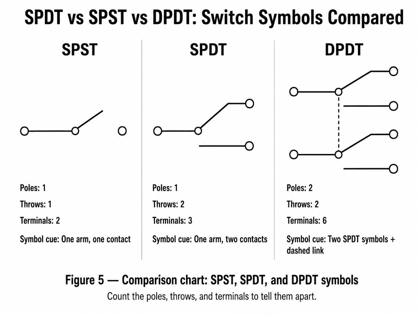
SPDT vs SPST vs DPDT: Switch Symbols Compared

These three are easy to tell apart once you count poles and throws:

  • SPST (Single Pole, Single Throw) — 1 pole, 1 throw, 2 terminals. A simple on/off switch; the symbol is one arm and one contact.
  • SPDT (Single Pole, Double Throw) — 1 pole, 2 throws, 3 terminals. One arm selecting between two contacts.
  • DPDT (Double Pole, Double Throw) — two SPDT switches operated together, 6 terminals. Drawn as two SPDT symbols joined by a dashed line showing the poles move as one.
Figure 5: SPST vs SPDT vs DPDT switch symbols compared, with terminal counts.

Comparison table:

Switch TypePolesThrowsTerminalsSymbol Cue
SPST112One arm, one contact
SPDT123One arm, two contacts
DPDT226Two SPDT symbols + dashed link

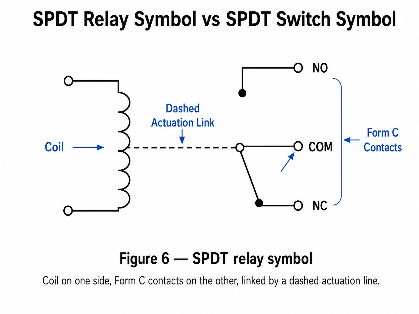
SPDT Relay Symbol vs SPDT Switch Symbol

A SPDT relay uses the same contact set as a manual SPDT switch—often called a Form C contact—but adds a coil. The symbol shows:

  • A coil (rectangle or loop) that, when energized, moves the contact.
  • The SPDT contact set: COM, NC, and NO.

When the coil is de-energized, COM connects to NC. Energize the coil, and COM switches to NO. So the difference between the switch and relay symbols is simply the added coil and the dashed line linking it to the moving contact.

Figure 6: The SPDT relay symbol — a coil plus Form C (COM/NC/NO) contacts.

How to Draw a SPDT Switch Symbol Step by Step

You can sketch a correct SPDT symbol in four steps:

  • Draw the common terminal (pole) as a dot or short line on the left—this is the input.
  • Draw two throw contacts on the right, one above the other—these are the two outputs.
  • Add the moving arm from the pole, angled so it touches one of the two throws.
  • Label the terminals: COM on the pole, NC and NO on the two throws.

For a DPDT, draw two of these stacked and connect the poles with a dashed line. For a relay, add a coil and link it to the arm with a dashed line.

FAQs About Switch SPDT Symbol

How many terminals does a SPDT switch have?
Three: one common (COM/pole) and two throws (often labeled NC and NO).

What do COM, NO, and NC mean on a SPDT symbol?
COM is the common pole (input). NC (normally closed) is connected to COM at rest. NO (normally open) connects to COM when the switch is actuated.

Is a SPDT switch the same as a changeover switch?
Yes. “Changeover” and “two-way switch” (British English) both describe a SPDT switch.

What’s the difference between the SPST and SPDT symbols?
SPST has one arm and one contact (2 terminals, on/off). SPDT has one arm and two contacts (3 terminals, selects between two outputs).

Can a SPDT switch be used as a SPST switch?
Yes—just use the common terminal and one throw, and leave the other throw unconnected.

Is a 2-way switch the same as SPDT?
Yes. “2-way switch” is the common British term for a SPDT switch, often used in staircase lighting.

Designing a electronic PCB board that uses SPDT switches, relays, or other components? EBest Circuit (Best Technology) is a one-stop PCB & PCBA contract manufacturer—send your Gerber files and BOM to sales@bestpcbs.com for a free DFM review.
You may also like