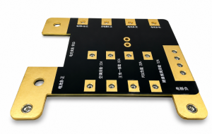
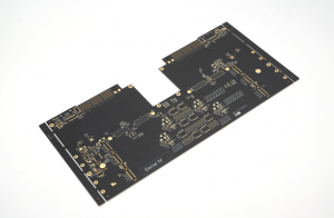
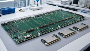
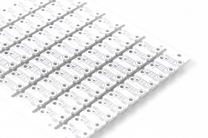
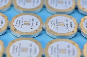
PCB manufacturing PCB manufacturing
Home > Blog

Top 10 Electronic Manufacturing Services UK Companies

August 25th, 2026

If you search for electronic manufacturing services UK, you are probably not looking for another simple definition of EMS. You may already have a product, a BOM, Gerber files, an urgent prototype, a cost target, or a production issue that needs a real manufacturing partner.

UK buyers often compare local EMS companies with overseas PCB and PCBA suppliers. Local support can be valuable for close communication, fast engineering meetings, and regulated product handover. A China-based PCB and PCBA partner can also be useful when the project needs competitive cost, special PCB manufacturing, component sourcing, small-batch PCBA, DFM review, or repeat production support.

EBest Circuit (Best Technology) is not a UK local factory. We are a China-based PCB and PCBA manufacturer serving global engineers and buyers, including UK customers who need practical support from PCB fabrication to component sourcing, SMT/THT assembly, inspection, testing support, and shipment. For RFQ review, send files to sales@bestpcbs.com.

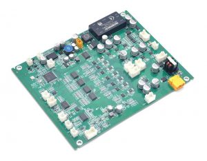
electronic manufacturing services UK
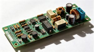
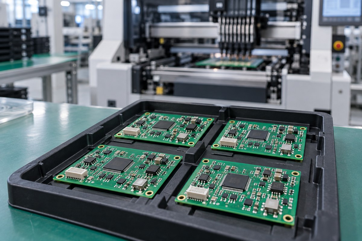
PCBA manufacturing support for UK buyers comparing EMS suppliers, cost, process capability, and delivery risk.

Top 10 Local Electronic Manufacturing Services UK Companies

A UK buyer may want a local EMS supplier for face-to-face engineering meetings, local logistics, product handover, repair support, or regulated industry communication. The companies below are useful examples to review when building a UK EMS shortlist. Always verify current capabilities, certifications, capacity, and quote scope directly before selecting a supplier.

UK EMS company Typical fit to check Buyer verification point
DSL Electronic Manufacture UK PCB assembly, box build, testing Warranty, AOI, design/manufacturing review
Protronix EMS PCB assembly, prototyping, cable assembly, turnkey EMS IPC-A-610, sourcing, traceability, production scale
Simtek EMS SMT, through-hole, full product build IPC training, AOI, industry fit
Arkle Electronics PCB assembly, cable harness, box build ISO, IPC standards, test scope
Jade Electronics High-reliability electronics manufacturing Traceability, ISO 9001, AS9100-oriented quality system
Jaltek Box build and complex electronic systems NPI, test, production transfer
EMS Technologies PCB assembly, wire harness, box build ISO 9001, AOI, production history
Active EMS Prototyping, DFM, purchasing, assembly, test Local support and supply-chain services
Active-PCB Solutions PCB assembly and EMS in Reading Conformal coating, inspection, box build
Microtech Electronics Turnkey EMS, prototypes, production, test Programming, logistics, quality control

This kind of list is only the first screen. The real decision starts when you compare quote details: what is included, what is excluded, what is tested, what is traceable, and what happens when a component or process detail changes.

UK vs China Electronic Manufacturing Services for PCBA Buyers

UK local EMS and China-based PCB/PCBA manufacturing solve different buyer problems. A local supplier may be the better choice when the project needs frequent in-person review, sensitive handover, local repair, or strict local production control. A China-based supplier can be attractive when the project needs special PCB processes, material options, component sourcing flexibility, lower unit cost, or scalable small-to-medium batch production.

A practical comparison for UK PCBA buyers:

Decision factor UK local EMS China PCB/PCBA partner
Engineering communication Easy local meetings and site visits Best when files, drawings, BOM, and test plan are clear
Prototype urgency Useful for local troubleshooting Useful when PCB, BOM, and assembly are coordinated together
Unit cost Often higher labor and overhead Often stronger for cost-sensitive repeat builds
PCB process options Depends on each local factory Strong when special PCB, MCPCB, ceramic, FPC, or rigid-flex is needed
Supply chain Local communication advantage Broad component sourcing and PCB supply-chain access
Risk control Local traceability and support Needs clear DFM, BOM review, inspection, and shipment plan

Many buyers do not choose only one model forever. They may use a UK EMS partner for early product handover and local builds, then use a China-based PCB/PCBA partner for cost-controlled prototype batches, special PCB fabrication, or repeat production. If you are comparing options, this related guide on PCB assembly UK can help you review supplier type and project fit.

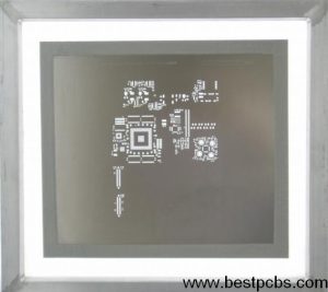
electronic manufacturing services UK
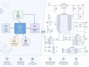
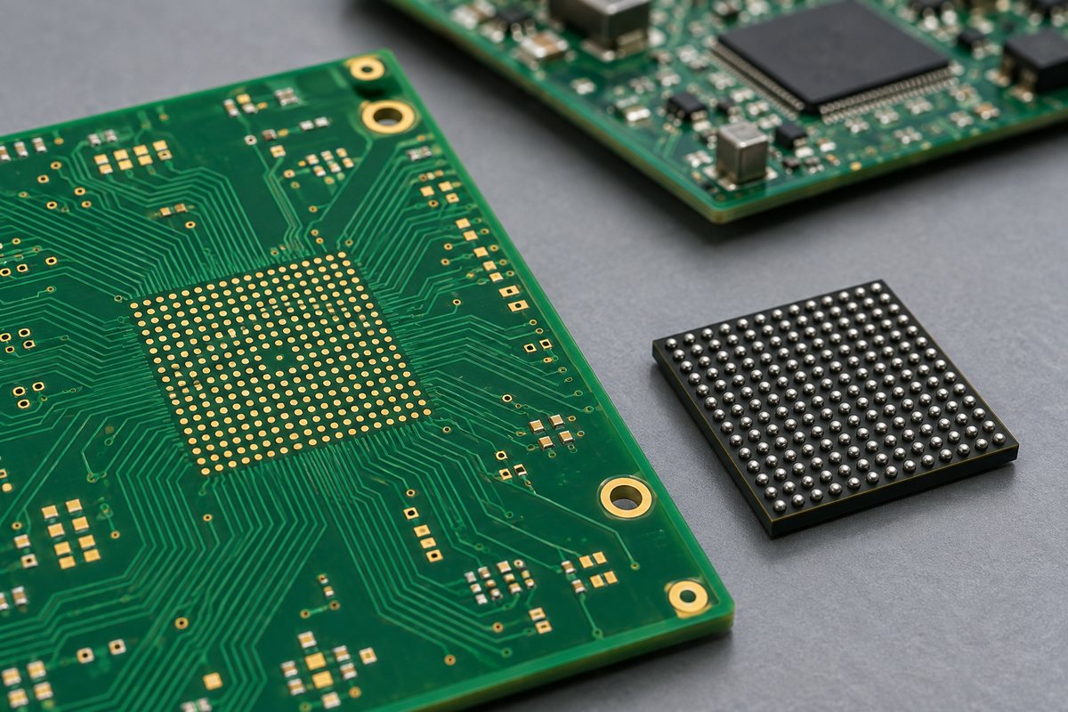
Before comparing EMS quotations, UK buyers should prepare the PCB files, BOM, drawings, quantity, test requirements, and delivery expectations.

Electronic Manufacturing Services UK Pricing: Local vs China Options

Pricing is not just the assembly unit price. A lower line-item quote can become expensive if it excludes sourcing work, test fixture preparation, engineering review, solder stencil, packaging, documentation, or failed-build risk. A higher quote may be reasonable if it includes better testing, traceability, production support, and fewer hidden handoffs.

For UK buyers, EMS pricing should be checked by total project cost:

  • PCB fabrication cost and special material cost
  • Stencil, tooling, fixture, and NPI charges
  • Component sourcing cost and shortage risk
  • SMT, THT, manual soldering, and mixed assembly labor
  • Inspection and test coverage
  • Engineering questions and DFM review time
  • Packaging, freight, customs, VAT, and landed cost
  • Cost of rework, delay, or production stoppage

A UK EMS quote may look more expensive at unit level but can reduce communication and handover risk for sensitive programs. A China PCB/PCBA quote may be more competitive for repeat builds, but it must include enough DFM review, BOM control, test support, and shipment planning to protect the project. The right comparison is not “UK price vs China price”; it is “which option gets usable assemblies into your schedule with acceptable risk?”

PCB and PCBA Process Support for UK EMS Orders from EBest Circuit

EBest Circuit supports UK EMS orders when the buyer needs a manufacturing partner that can review files, fabricate PCBs, source components, assemble boards, and support inspection or testing under one coordinated workflow. This is especially useful when the UK buyer has a clear design package but wants fewer supplier handoffs.

For a UK EMS order, EBest Circuit can support:

  • Gerber, ODB++, drill, stackup, and fabrication note review
  • DFM pre-review before production release
  • BOM review, availability check, and sourcing suggestions
  • PCB fabrication for FR4, multilayer, MCPCB, ceramic, FPC, rigid-flex, high-frequency, and special PCBs
  • SMT, through-hole, and mixed PCBA assembly
  • AOI, visual inspection, X-ray for suitable assemblies, and functional testing support
  • Prototype, small-batch, and repeat production support
  • Shipment planning for UK delivery requirements

The value is not only that one supplier can quote more items. The value is that the PCB process, BOM risk, assembly method, inspection plan, and delivery schedule can be reviewed together before the buyer places the order.

Certifications UK Buyers Can Verify Before Electronic Manufacturing Projects

Certifications do not replace project review, but they help UK buyers screen whether a supplier has a quality system suitable for the product risk. Before placing an electronic manufacturing project, buyers should ask which certifications apply to the actual factory, process, product type, and shipment documents.

EBest Circuit holds quality certifications including ISO 9001, ISO 13485, IATF 16949, AS9100D, REACH, RoHS, and UL-related support. For buyers in medical, automotive, aerospace, industrial, and controlled electronic assemblies, these certifications can help with supplier qualification before the RFQ moves into technical review.

Important certification checks include:

  • Does the certificate name match the supplier entity or factory being used?
  • Is the certificate valid during the planned production period?
  • Does the certification scope match PCB fabrication, PCBA assembly, or both?
  • Does the buyer need RoHS, REACH, UL material evidence, CoC, or test records?
  • Does the project require automotive, medical, aerospace, or other controlled documentation?

Certification is strongest when it is connected to the actual build plan: materials, approved suppliers, work instructions, inspection records, lot traceability, and final shipment documentation.

PCB and PCBA Process Capability for UK Production Builds

Production capability should be judged by what the supplier can manufacture repeatedly, not by a long capability list alone. For UK production builds, the buyer should confirm PCB type, layer count, copper requirement, board thickness, surface finish, component package, assembly method, inspection method, test plan, and order volume.

EBest Circuit provides customized PCB and PCBA support across standard and special technologies. Monthly PCB capacity is about 260,000 square feet, and more than 1,000 different board types can be completed. For assembly, the process can support SMT, through-hole, and mixed PCBA builds, including engineering review before production.

Item EBest Circuit support
PCB types FR4, multilayer, MCPCB, ceramic, FPC, rigid-flex, high-frequency, special PCB
SMT capability 01005 parts, 0.25mm BGA pitch, up to 13.2M chips/day placement capacity
Board size 0.2 x 0.2 in to 20 x 20 in; long panel support up to 22 x 47.5 in
Assembly methods SMT, THT, mixed assembly; reels, cut tape, tubes, trays, and loose parts
Engineering support DFM review, BOM sourcing, inspection, testing support, traceability

This type of capability is useful for UK buyers who do not want to split PCB fabrication, component sourcing, and PCBA across too many vendors. It also helps when the design includes special PCB materials, non-standard stackups, or mixed assembly requirements.

Lead Time Support for UK PCBA Prototype and Production Orders

Lead time is one of the main reasons UK buyers compare EMS suppliers. The schedule is not controlled only by assembly speed. It depends on file readiness, PCB technology, component availability, stencil preparation, DFM closure, engineering questions, test preparation, production capacity, packing, freight, and customs.

Lead time should be planned by the bottleneck, not by the fastest process step:

Build type Typical planning window Fastest support when suitable
Standard FR4 prototypes, 1-4 layers 7-10 days 24-48 hours
Higher-layer FR4, 6-8 layers 10-12 days About 72 hours
1-layer MCPCB prototypes About 4 days About 24 hours
Special PCB builds Usually planned by stackup and material Confirmed after engineering review
PCBA after materials are ready 1-5 days assembly window Urgent suitable builds can be faster

For suitable PCBA projects, EBest Circuit can support fast delivery, including around 1.5-week PCBA turnaround when project files, materials, engineering conditions, and production capacity are ready. This is useful for UK prototype validation, small-batch builds, and urgent production support. It should still be confirmed case by case before the buyer commits the customer delivery date.

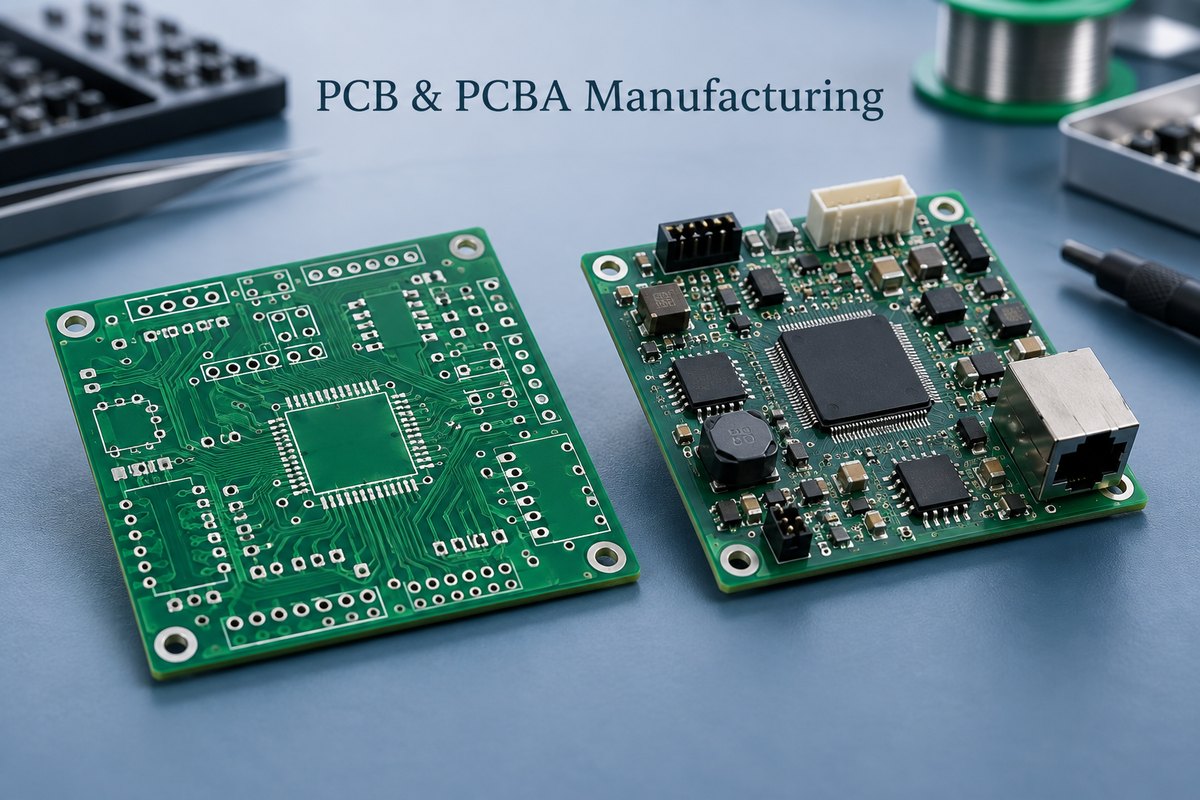
electronic manufacturing services UK
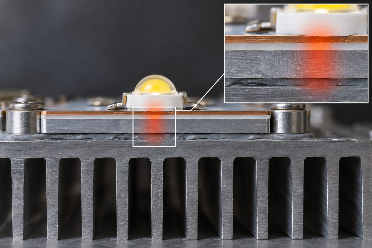
Inspection and functional testing preparation help protect UK PCBA prototype and production schedules.

UK PCBA Project Case Study with EBest Circuit Support

A UK industrial automation buyer contacted EBest Circuit for a small-batch PCBA project after the first local quotation exceeded the target budget. The product was a control module used inside an equipment cabinet. The buyer needed a repeatable build, not only a few prototype boards.

Project requirements:

  • Country: United Kingdom
  • Application: industrial control module for equipment monitoring
  • PCB type: 4-layer FR4 control board with mixed SMT and through-hole connectors
  • Quantity: 50 pcs prototype validation, then 300 pcs pilot order
  • Buyer concern: BOM risk, connector orientation, test access, and schedule control
  • Required support: PCB fabrication, component sourcing, SMT/THT assembly, inspection, and functional test preparation

Main challenges:

  • Two connector footprints had similar bodies but different pin directions.
  • Several ICs had alternative part numbers with different lead times.
  • The original test pads were too close to the enclosure edge.
  • The buyer wanted a pilot batch quickly, but the BOM was not fully locked.

EBest Circuit solution:

  • Our engineering team reviewed Gerber, BOM, centroid, and assembly drawings before quotation finalization.
  • The BOM sourcing team marked long-lead and alternative parts for buyer approval.
  • The DFM review flagged connector orientation and test-point access before PCB release.
  • SMT and THT assembly were planned in one sequence to reduce rework risk.
  • Inspection and functional test preparation were aligned before pilot production.

The result for the buyer was a clearer production path: one supplier managed PCB fabrication, component sourcing, PCBA assembly, and inspection communication. The project still required buyer approval for alternatives and test details, but the RFQ moved from a simple price comparison to a controlled build plan.

Why UK Buyers Choose EBest Circuit for PCB and PCBA Manufacturing

UK buyers choose EBest Circuit when they need more than a bare PCB quote. Many projects require a supplier that can review the manufacturing files, catch assembly risks, source components, support special PCB types, and help the project move from prototype to repeatable production.

EBest Circuit is a practical option when UK buyers need:

  • One-stop PCB fabrication, component sourcing, PCBA assembly, and testing support
  • DFM pre-review and BOM optimization before production
  • Support from 1 business representative and 3 engineers through the project flow
  • Manufacturing input from engineers with long PCB and PCBA experience
  • Prototype and small-batch support for design validation
  • ISO 9001, ISO 13485, IATF 16949, AS9100D, REACH, RoHS, and UL-related quality support
  • Own PCB and PCBA factory resources plus a 1,000+ supplier network
  • Digital workshop traceability for material, batch, production cycle, and production progress

For buyers who are still defining the service scope, this article on EMS manufacturing explains the wider manufacturing model. If the project includes UK-specific supplier comparison, related topics such as PCB manufacturer UK and flexible PCB manufacturer UK may also help buyers screen options before sending the RFQ.

FAQs About Electronic Manufacturing Services UK Companies

Should UK buyers always choose a local EMS company?

No. A local EMS company can be valuable for face-to-face communication, regulated product handover, or local service support. A China-based PCB/PCBA partner can be better when the buyer needs special PCB processes, competitive cost, sourcing flexibility, or small-batch manufacturing support.

What files should I send for an EMS quotation?

Send Gerber or ODB++ files, BOM, centroid or pick-and-place file, assembly drawings, quantity, surface finish, test requirements, delivery destination, and any special packaging or inspection requirements. Clear files reduce quote delay and engineering questions.

Can EBest Circuit support both PCB fabrication and PCBA assembly?

Yes. EBest Circuit supports PCB fabrication, component sourcing, SMT assembly, through-hole assembly, mixed assembly, inspection, and testing support. This is useful when UK buyers want fewer handoffs between PCB supplier, component supplier, and assembly supplier.

How should UK buyers compare EMS quotations?

Compare total delivered value, not only unit price. Check PCB cost, BOM sourcing, assembly labor, tooling, test fixture, inspection records, delivery schedule, freight, customs, and the cost of delay or rework.

What makes an EMS supplier reliable for repeat production?

A reliable supplier should control BOM sourcing, approved alternatives, DFM records, process flow, inspection method, test plan, lot traceability, packaging, and delivery communication. Repeatability matters more than a low first quote.

In Conclusion, electronic manufacturing services UK buyers should compare local EMS companies and China-based PCB/PCBA partners by cost, process capability, certifications, lead time, risk control, and production repeatability. If you need PCB fabrication, component sourcing, PCBA assembly, DFM review, inspection, or testing support for a UK project, contact EBest Circuit (Best Technology) at sales@bestpcbs.com.

You may also like

PCB Panelization Approval: Prevent Costly Production Changes

August 25th, 2026

A PCB panelization drawing is not just a convenient way to place several boards on one manufacturing panel. It defines how the boards will be fabricated, handled, assembled, separated, counted and delivered. If those decisions are left unclear, a technically correct PCB can still require a new quotation, a revised fixture, manual handling or a last-minute production change.

The practical goal is simple: approve the panel before it becomes a production constraint. This guide helps PCB engineers and buyers decide who should create the array, what the manufacturer needs to review, and which details must be frozen before fabrication and assembly begin.

panelization
Review the PCB panel, production drawing and delivery format before production approval.

What Should Be Confirmed Before PCB Panelization?

Panelization should begin with the required production and delivery flow—not with a target number of boards per panel. Before a panel drawing is created, confirm the following points.

  • Required delivery unit: Will the supplier deliver individual PCBs, complete panels or assembled boards separated after SMT?
  • Single-design or mixed panel: Will every position contain the same design, or must several part numbers share one panel?
  • Quantity basis: Is the order and quotation based on individual pieces or complete panels?
  • Downstream process: Will the panel pass through solder paste printing, pick-and-place, reflow, AOI, functional testing or another fixture-dependent process?
  • Allowed panel changes: May the fabricator rotate boards, change the up count or adjust the rails to improve manufacturability?
  • Depaneling responsibility: Will separation occur at the PCB factory, PCBA factory or customer site?
  • Quality rules: Are X-outs allowed? Are panel-level traceability, coupons, electrical testing or special packaging required?

These answers create the design boundary. Without them, two suppliers can interpret the same Gerber package differently and return quotations that do not cover the same deliverable.

The board construction also matters. A standard FR4 PCB may allow several practical layouts, while a thin flexible circuit, brittle ceramic substrate, heavy-copper board or impedance-controlled multilayer design can impose additional handling and process limits.

Who Should Control the Panelization Design?

Who should control the layout depends on the equipment and downstream processes the panel must fit.

Let the PCB manufacturer create the panel when:

  • You are supplying a single-board Gerber package.
  • The main objective is manufacturability and material utilization.
  • No customer-owned pallet, stencil or assembly fixture fixes the panel dimensions.
  • The manufacturer may adjust rails, spacing and orientation within agreed limits.

In this situation, send the finished board data and the required delivery conditions. The fabricator can propose a production panel based on its process and working-panel format. You should still review the production drawing before release.

Supply or control the array when:

  • A stencil, carrier, test fixture or automated line already depends on a fixed outline.
  • Several different boards must be delivered as one matched set.
  • Board orientation is controlled by a connector, sensor, coating or assembly requirement.
  • The panel must match an approved repeat-order configuration.
  • Traceability or packaging is managed at panel level.

The safest handoff is a documented division of responsibility. The customer defines the functional and downstream constraints, while the manufacturer confirms that the proposed panel can be fabricated, assembled and separated without creating avoidable risk.

Do not assume that an old panel should automatically be reused. A change in laminate, copper weight, board thickness, component placement, assembly site or delivery format can make the previous array unsuitable even when the circuit revision appears minor.

How Should PCB Panelization Methods Match the Board?

The best separation method is the one that fits the board outline, component layout, material and downstream handling—not simply the least expensive cutting process.

  • V-scoring is usually considered when boards have straight shared edges and can be arranged in rows. It can support efficient separation, but the score line and remaining web must be reviewed against board thickness, copper distribution and nearby components. Components, solder joints and brittle features should not be placed where bending during separation can transfer damaging stress.
  • Tab routing is useful for irregular outlines or layouts that cannot share continuous straight edges. Routed gaps define most of the finished profile, while tabs keep each board connected to the array. Tab position, width and removal method should be agreed before production. Poorly positioned tabs can leave difficult edge cleanup or transfer force toward sensitive areas.
  • Mouse-bite perforations can make manually removed tabs easier to break, but hole size, pitch and distance from the finished edge affect the remaining witness marks. If the enclosure requires a smooth edge, secondary finishing or a different tab strategy may be needed.
  • Mixed-design panels may reduce handling for matched products, but they require additional control. The designs must be compatible in material, thickness, copper build, surface finish, process route and delivery quantity. Combining unrelated boards only to fill open space can complicate fabrication, assembly and quality disposition.

Special constructions require more than a generic rectangular array:

  • A rigid flex PCB may need temporary support and careful control of the flexible areas.
  • A ceramic PCB is brittle, so separation force and edge damage need particular attention.
  • Heavy-copper and asymmetrical multilayer boards may require warpage review.
  • Thin boards and FPCs may depend on tooling or carriers for stable assembly handling.
  • Impedance-controlled boards require the approved stackup and coupon strategy to remain aligned with the production panel.

This is why PCB panelization methods should be selected after the manufacturer reviews the actual build—not copied from a visually similar board.

panelization
V-scoring and routed breakaway tabs must match the board outline, material and separation requirements.

How Do PCB Panel Size and Array Quantity Affect Cost?

More boards per panel do not automatically mean a lower total cost. The better question is whether the selected PCB panel size creates a stable, repeatable route through fabrication and assembly.

The real panel cost is influenced by:

  • The usable manufacturing area and required process margin.
  • Board outline, rotation and spacing.
  • Rail width and routing channels.
  • Tooling holes, fiducials, coupons and identification areas.
  • Material type, copper weight, layer count and stackup.
  • Fabrication yield and the policy for defective units within a panel.
  • SMT line limits, stencil dimensions and fixture size.
  • Whether the supplier ships by piece or by complete panel.

For example, increasing an array from four boards to six may improve laminate utilization, but it can also make the panel less rigid, exceed an assembly-line limit or increase the commercial impact of one rejected panel. Conversely, an array with generous unused space may be justified when it provides the rails, support and keep-outs required for stable processing.

Buyers should request a quotation that states:

  • Finished board size.
  • Proposed panel size.
  • Number of boards per panel.
  • Number of panels and total good-board quantity.
  • Whether X-outs are permitted.
  • Whether the price includes depaneling.
  • Whether assembly and final delivery are quoted per panel or per finished board.

This removes a common source of price confusion: two quotations may show the same piece quantity while assuming different panel counts, separation work or acceptable panel yield.

How Should Panel Design Support Assembly and Depaneling?

A fabrication-efficient array can still be inconvenient for PCBA. The panel should be reviewed as a temporary production tool that must remain stable from solder paste printing through final separation.

For automated assembly, check:

  • Rails provide sufficient support for conveyors and board handling.
  • Global fiducials and tooling holes match the assembler’s requirements.
  • Component orientation supports the intended process flow.
  • Edge components, connectors and overhanging parts have enough clearance.
  • The panel remains sufficiently rigid through printing, placement and reflow.
  • Barcode, serial-number and traceability locations remain accessible.
  • Test points and fixtures can reach the required locations.

For depaneling, check:

  • Score lines or tabs do not intersect copper, plated features or sensitive areas.
  • Tall, heavy, ceramic or brittle components are kept away from high-stress separation zones.
  • The selected tool can access every separation path.
  • Edge quality is suitable for the enclosure or mechanical interface.
  • The separated board can be handled and packaged without damaging protruding parts.

If one supplier handles both PCB fabrication and prototype PCB assembly, the panel can be reviewed against the real SMT flow before the first build. The customer retains final approval, while the combined review reduces handoff gaps between a fabrication-only drawing and the assembly process that follows.
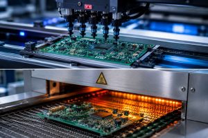
panelization
Tooling rails, fiducials and panel rigidity help the array move reliably through SMT assembly.

What Should Be Reviewed Before Production Approval?

The production panel drawing should turn assumptions into visible, reviewable requirements. Before approval, compare it with the released board files, assembly information and purchase requirements.

Review at least these items:

  • Revision identity: Board part number, revision and file date match the released package.
  • Finished outline: Board dimensions, slots, cutouts and critical tolerances are correct.
  • Array definition: Panel dimensions, up count, orientation and mixed-board arrangement are identified.
  • Separation features: V-scores, routed gaps, tabs and mouse bites are dimensioned and correctly located.
  • Manufacturing rails: Rail width, tooling holes, fiducials, coupons and markings are included where required.
  • Component clearance: Assembly keep-outs and edge-component risks have been checked.
  • Stackup and material: Thickness, laminate, copper build and impedance requirements match the approved construction.
  • Quality disposition: X-out rules, test requirements and acceptance criteria are recorded.
  • Delivery format: Panel delivery, individual-board delivery or post-assembly separation is stated.
  • Packaging and traceability: Panel quantity per package, labels, date codes and protective packaging are defined.

Record technical questions and answers in a controlled engineering-query log. If the fabricator changes the up count, orientation, score position, tooling rail or stackup, the revised drawing should be approved before production rather than accepted through an informal message.

For repeat orders, confirm that the approved panel revision still matches the current PCB, BOM, assembly drawing and delivery requirement. A previously manufactured panel is useful evidence, but it is not a substitute for revision control.

PCB Panelization Case Study: From Panel Approval to Assembly

A two-layer PCB project shows why panel approval must cover fabrication, assembly and final delivery—not just the number of boards in an array.

The project used a two-layer PCB with 370HR material, 1.5 oz copper, a finished thickness of 1.57 mm with tolerance, ENIG and IPC Class 3 requirements. The fabrication record also specified plugged vias, identification markings and electrical testing.

The important panelization decision was not simply how many boards could fit on a working panel. The documented production flow required:

  • The blank-board manufacturer to create the production panel.
  • The production panel drawing and stackup to be sent for customer confirmation.
  • Bare PCBs to be electrically tested before assembly.
  • Bare boards to be delivered in panel form for lead-free SMT.
  • Finished assemblies to be separated and delivered as individual boards.
  • Final assembled boards to use antistatic packaging.

This sequence created three different definitions that had to remain consistent: the individual PCB design, the fabrication panel and the post-SMT delivery unit. If the quotation had stated only the number of individual boards, it would not have fully described the required work.

The approval review therefore needed to verify the panel outline, rails, fiducials, tooling provisions, up count, stackup, assembly handling and final separation responsibility. The value came from connecting fabrication data with assembly and delivery requirements before production began, instead of treating panelization as an isolated CAM step.

For buyers, the practical lesson is to approve the full route—not only the Gerber image. A panel is temporary, but the decisions built into it affect every board passing through the line.

panelization
Panel approval connects bare-board fabrication, assembly handling and individual-board delivery.

FAQs About PCB Panelization

Should I include a panelized Gerber file when requesting a quotation?

You may provide one when a fixed array is required, but also include the single-board Gerber data and clearly identify which file controls production. If no fixture or downstream constraint fixes the array, sending the single-board data plus your delivery requirements allows the manufacturer to propose a manufacturable panel.

Can a PCB manufacturer change my panelization design?

The manufacturer may recommend changes to spacing, rails, tooling features, orientation or separation details. No production-affecting change should be assumed automatically. The proposed production drawing and any engineering questions should be reviewed and approved through revision control.

Is V-scoring always cheaper than tab routing?

Not in every project. V-scoring can be efficient for boards with compatible straight edges, while routed tabs suit many irregular outlines. The total cost also depends on material utilization, routing time, assembly handling, edge-quality requirements and the selected depaneling process.

Can different PCB designs be placed on the same panel?

Yes, when the designs and manufacturing routes are compatible. Material, thickness, copper build, surface finish, process steps, assembly requirements and quantities must be reviewed together. A mixed panel should solve a production or delivery need, not merely fill unused space.

What files are needed for a panelization review?

Send the released single-board Gerber or ODB++ package, NC drill data, fabrication drawing, stackup and impedance requirements. For assembled products, also send the BOM, centroid or pick-and-place file, assembly drawings, component height information, required delivery format and any stencil, pallet, fixture or test constraints.

Before approving your next panel, send EBest Circuit (Best Technology) the released PCB files, assembly requirements and intended delivery format. You work with one dedicated sales contact backed by three engineers, giving you one communication channel for manufacturability review, PCB fabrication, component sourcing and PCBA assembly. For a panelization and DFM review, contact sales@bestpcbs.com.

Confirm the PCB panelization route before production so the quotation, fabrication panel, SMT process and final delivery unit describe the same product.

You may also like

Electronics NPI Services in China for a Smoother Launch

August 25th, 2026

Electronics NPI services help new products reach production without avoidable late-stage surprises. Delays often begin when stack-up issues, unavailable components, assembly constraints, or test requirements are discovered only after production has been scheduled.

EBest Circuit provides electronics NPI services in China covering PCB manufacturability review, PCB fabrication, BOM sourcing, SMT and through-hole assembly, inspection, programming, and customer-defined testing assistance. Send your project package to sales@bestpcbs.com to identify manufacturing and sourcing risks before placing the order.

electronics NPI services
Electronics NPI manufacturing review connects PCB files, BOM sourcing, assembly, and inspection before production.

Why Buy Electronics NPI Services in China?

The commercial value is not simply access to lower manufacturing costs. The larger benefit is having PCB fabrication, component sourcing, assembly, inspection, and shipment planning reviewed as one connected order.

When those activities are divided among unrelated suppliers, each handoff creates another place for assumptions to change. The PCB fabricator may approve a stack-up that the assembly supplier has not reviewed. The sourcing company may propose a component substitution without checking package, lifecycle, or assembly constraints. Test requirements may arrive only after the first boards have been assembled.

A coordinated NPI scope can reduce these avoidable handoffs:

  • one controlled PCB and PCBA revision for quotation and production;
  • earlier confirmation of board materials, stack-up, surface finish, and special processes;
  • BOM availability and substitution questions raised before purchasing;
  • assembly and inspection requirements reviewed before the pilot build;
  • one documented route for engineering questions and customer approvals;
  • clearer responsibility for packaging, shipment, and production records.

For overseas customers, this coordination can also reduce repeated communication, separate shipments, and duplicated logistics work. It does not remove the customer’s responsibility for product design, certification, firmware, or final product validation. It gives the released design a clearer path through PCB and PCBA manufacturing.

What Should NPI Contract Manufacturing Include?

A useful NPI quotation should show exactly what the supplier will deliver. Two prices cannot be compared fairly if one covers only bare PCB fabrication while the other includes sourcing, assembly, X-ray inspection, and testing assistance.

Define the manufacturing scope before comparing prices:

  • PCB layout manufacturability review against the released data;
  • bare PCB fabrication and the agreed material or stack-up;
  • BOM sourcing responsibility and approved substitution rules;
  • customer-supplied component handling, when applicable;
  • SMT and through-hole assembly;
  • cleaning, conformal coating, depaneling, or other specified processes;
  • AOI, X-ray, electrical inspection, and workmanship acceptance requirements;
  • programming or customer-defined functional testing assistance;
  • reports, traceability, packaging, and shipment requirements.

EBest Circuit focuses on PCB and PCBA manufacturing execution. Your product-development team can continue managing circuit design, firmware, RF architecture, certification, and final product compliance with its chosen specialists. This division gives each team a clear role while keeping manufacturing questions connected to the actual files and order requirements.

Can Your Supplier Handle the PCB Technologies in Your NPI Builds?

An NPI supplier should be selected for the actual board, not for a general claim such as “we manufacture multilayer PCBs.” A prototype can stall after quotation if the supplier later discovers that the requested bend area, ceramic construction, copper weight, impedance geometry, or material combination does not fit its process.

Confirm technology fit while changes are still manageable:

  • FPC and rigid-flex PCB: review bend regions, stiffeners, coverlay openings, flex-to-rigid transitions, and assembly handling;
  • HDI PCB: confirm microvia structure, sequential lamination, via filling, registration, and stack-up feasibility;
  • high-frequency PCB: confirm the specified laminate, copper profile, stack-up, impedance requirements, and material availability;
  • thick-copper PCB: review copper weight, spacing, thermal balance, finished thickness, and assembly implications;
  • ceramic PCB: confirm substrate type, metallization, dimensional requirements, and process availability;
  • MCPCB: review dielectric construction, copper thickness, thermal path, board flatness, and assembly requirements;
  • extra-thin PCB: confirm handling, panelization, warpage control, and thickness tolerance;
  • PCBA: review component packages, polarity, clearances, soldering process, inspection access, and test points.

Keep fine-pitch and mixed-technology assembly within one reviewed workflow:

Assembly item Capability
Minimum SMD component 01005
Minimum BGA pitch 0.25 mm
Assembly types SMT, THT, and mixed assembly
Component packaging Reels, cut tape, tubes, trays, and approved loose parts

These figures are useful starting points, but each project still needs a file review. Pad geometry, stencil design, moisture sensitivity, reflow compatibility, board warpage, and inspection access may affect the final process.

Your product team defines the electrical, thermal, mechanical, and compliance requirements. EBest Circuit reviews whether the proposed construction can be manufactured, identifies conflicts, and requests confirmation before a material or process change is made.

This early check is especially valuable for medical, industrial-control, automotive, communications, AI-hardware, semiconductor, sensor, and LED projects, where a late material or process change can affect more than the PCB price. It may force another assembly trial, another approval cycle, or a revised delivery commitment.

electronics NPI services
Fine-pitch SMT capability should be confirmed against the actual PCB and component package.

How Will Your Supplier Control the NPI Supply Chain Process?

A buildable PCB does not guarantee a buildable PCBA. Component availability, package compatibility, moisture sensitivity, lifecycle status, and approved-alternative rules can stop the order after PCB production has already started.

A controlled NPI supply chain process should make these risks visible before purchasing:

  • manufacturer name and exact manufacturer part number for each BOM line;
  • quantities, reference designators, and do-not-install items;
  • lifecycle, availability, and lead-time review for critical parts;
  • package, value, tolerance, voltage, and temperature-rating checks;
  • approved alternates and the person authorized to approve deviations;
  • customer-supplied parts, expected arrival date, and incoming condition;
  • moisture-sensitive and special-storage requirements;
  • traceability or date-code requirements;
  • shortage, minimum-order, and excess-material assumptions.

A low unit price is not helpful if it depends on an unapproved substitute or an unrealistic component lead time. Ask the supplier to separate confirmed material, proposed alternatives, and unresolved lines in the quotation.

For a pilot order, it is also useful to identify which components may limit repeat production. If a prototype depends on obsolete, broker-sourced, or allocation-controlled parts, your team should know that before approving the production plan.

electronics NPI services
Early BOM and component review makes sourcing risks visible before purchasing.

What Must NPI Prototyping Prove Before Production?

The purpose of NPI prototyping is not merely to produce a small quantity of working boards. It should provide evidence that the released PCB and PCBA package can be manufactured, inspected, and repeated under the agreed conditions.

Use the prototype or pilot build to close practical manufacturing questions:

  • Does the fabricated PCB match the approved material, stack-up, thickness, finish, and impedance requirements?
  • Do components fit the footprints, polarity markings, and mechanical clearances?
  • Can the assembly be soldered without unacceptable bridging, voiding, opens, or thermal damage?
  • Are fine-pitch, BGA, QFN, connector, and through-hole areas accessible to the required process and inspection methods?
  • Is the panelization suitable for assembly, depaneling, and handling?
  • Can the agreed inspection and test steps be completed with the available files, fixtures, firmware, and limits?
  • Are deviations, rework, and customer approvals recorded against the correct revision?

The result should be a decision package, not only a box of boards. Depending on the order, this may include first-article measurements, AOI records, X-ray images, electrical-test results, workmanship findings, functional-test results supplied under the customer’s procedure, and a list of open issues.

Before placing a volume order, confirm which issues are closed, which changes were approved, and which risks remain customer-owned. This makes the production release easier to approve and reduces the chance that an undocumented prototype exception becomes the next lot’s standard process.

electronics NPI services
X-ray and inspection evidence helps the customer approve the NPI build for the next stage.

How Should You Compare an NPI Manufacturing Service Quote?

The lowest quoted price can become the most expensive option if it excludes material control, engineering review, inspection, or the work needed to make the second build repeatable. Compare the assumptions behind the price, not only the total.

Check these items side by side:

  • exact PCB material and construction;
  • quoted PCB technology and special-process limits;
  • component sourcing scope and substitution policy;
  • prototype, pilot, and expected production quantities;
  • tooling, stencils, fixtures, programming, and test charges;
  • engineering questions and customer-approval route;
  • inspection, X-ray, test, and report deliverables;
  • certification or qualification documents that can actually be supplied;
  • lead time for material, fabrication, assembly, and shipment;
  • packaging, freight, duties, and other commercial assumptions;
  • control of approved revisions for the next order.

Price pressure is real, but a usable quotation should tell you what will happen after the purchase order is issued. A supplier that identifies an unavailable construction, a risky BOM line, or a missing test fixture before order placement may protect the launch better than a supplier that returns a fast price with silent assumptions.

For complex or high-reliability projects, ask which evidence will support acceptance. Certification claims should be specific and relevant to the ordered scope; they should not replace project-specific manufacturing and inspection records.

What Lead Time Can You Expect for NPI Builds?

An attractive quotation is not useful if the production window misses your launch date. Ask the supplier to separate material availability, PCB fabrication, assembly, inspection, testing, and shipping instead of providing one unexplained delivery estimate.

Use these indicative production times to evaluate whether EBest Circuit may fit your NPI schedule.

PCB fabrication for qualified standard prototypes below 1 m²

Prototype type Normal production Expedited production
1–2 layer standard FR-4 7–8 days As fast as 24 hours
4-layer standard FR-4 10 days As fast as 48 hours
6-layer standard FR-4 10 days As fast as 72 hours
8-layer standard FR-4 12 days As fast as 72 hours
Single-layer standard MCPCB 4 days As fast as 24 hours

PCBA production after PCBs, components, and assembly files are ready

Assembly service Normal production Expedited production
PCBA Approximately 1 week As fast as 2 days

These figures refer to production time, not delivery to your facility. The confirmed schedule depends on the files, material and component availability, quantity, process complexity, inspection, testing, and current production capacity.

Put the required arrival date in your RFQ.

Also include the shipping destination and preferred shipping method. EBest Circuit can then separate production time from transit time and check whether normal or expedited service can support your schedule. Expedited production requires confirmation and may involve an additional fee.

Why Use EBest Circuit for PCB Assembly NPI?

EBest Circuit is positioned for customers who already have a released or near-released design and need a manufacturing partner to turn it into a controlled PCB and PCBA order. Our role is to connect manufacturability review, PCB production, sourcing, assembly, and agreed verification activities without claiming ownership of the customer’s complete product design.

Your team can use one manufacturing contact for:

  • PCB file and manufacturability review;
  • FPC, rigid-flex, HDI, high-frequency, thick-copper, ceramic, MCPCB, extra-thin, and conventional multilayer PCB requirements;
  • BOM review and component sourcing;
  • SMT and through-hole assembly;
  • AOI, X-ray, workmanship inspection, and agreed testing assistance;
  • prototype, pilot, and repeat-production quotation support;
  • documented engineering questions and customer-approved changes.

This combination is useful when the main commercial risk is not one isolated manufacturing step, but the handoff between steps. One team reviewing the PCB, BOM, assembly, and inspection package can identify mismatched revisions and missing information earlier.

Your specialists can continue managing electrical, mechanical, thermal, RF, firmware, regulatory, and final product-reliability decisions. EBest Circuit reviews the manufacturing package, raises producibility questions, builds to the agreed scope, and supports the inspection and testing activities defined for the order.

What Files Should You Send for an Electronics NPI Services Quote?

A complete RFQ helps the supplier identify process conflicts, material risks, and missing deliverables before pricing. It also makes competing quotations easier to compare because each supplier is reviewing the same released package.

Send the files and commercial details that define the order:

  • Gerber or ODB++ fabrication data;
  • NC drill files and fabrication drawing;
  • approved or reference stack-up;
  • controlled-impedance requirements, if applicable;
  • BOM with manufacturer part numbers;
  • centroid or placement data;
  • assembly drawings and polarity references;
  • panelization requirements, if already defined;
  • prototype quantity and expected production quantities;
  • customer-supplied component list and arrival timing;
  • approved-alternative and deviation rules;
  • workmanship, inspection, X-ray, programming, and test requirements;
  • required reports, traceability, packaging, and delivery date.

If a requirement is not yet final, mark it as pending instead of allowing each supplier to make a different assumption. For complex PCBs, identify the features that drive the project, such as flex construction, microvias, ceramic substrate, high-frequency material, thick copper, thermal requirements, or extra-thin finished thickness.

Email the released package to sales@bestpcbs.com. EBest Circuit can review the PCB/PCBA manufacturing scope, identify information needed for quotation, and clarify which fabrication, sourcing, assembly, inspection, and testing activities can be included.

FAQs About New Product Introduction Services

Can EBest Circuit quote bare PCBs without assembly?

Yes. The RFQ can cover bare PCB fabrication only, PCB plus customer-supplied component assembly, or a broader package including BOM sourcing and PCBA. State the required outcome so the quotation matches your purchasing plan.

Can we supply some or all components?

Yes, subject to agreement. Provide the customer-supplied part list, quantities, expected delivery date, packaging condition, moisture-sensitivity information, and rules for shortages or damaged parts.

Can you support a small prototype before production?

Prototype and pilot quantities can be reviewed as part of the quotation. Include the expected follow-on quantity because material purchasing, tooling, panelization, and test planning may differ between a few prototypes and repeat production.

Will EBest Circuit approve component substitutions?

No supplier should approve a design substitution on the customer’s behalf unless that authority is explicitly granted. We can identify sourcing risks and propose alternatives for customer review. The customer or its authorized design owner approves the final substitution.

What inspection and testing can be included?

The available scope depends on the product and the released requirements. It may include PCB electrical testing, AOI, X-ray, workmanship inspection, dimensional checks, programming assistance, and customer-defined functional testing assistance. The quotation should state what is included and what fixtures, firmware, procedures, and acceptance limits the customer must provide.

Do you provide complete product design and certification?

EBest Circuit supports the PCB and PCBA manufacturing portion of NPI. Your chosen specialists can continue handling complete product design, firmware development, certification, and final product approval.

What usually delays an electronics NPI services quote?

Common causes include an incomplete BOM, missing fabrication drawing, unclear PCB revision, no approved stack-up, unspecified substitutions, missing placement data, undefined test scope, and no target quantities. Sending these items together reduces assumptions and shortens the clarification cycle.

Choosing an electronics NPI services partner is ultimately a decision about controllability. A clear scope, confirmed PCB capability, visible supply-chain risks, documented prototype evidence, and a complete RFQ give your team a stronger basis for approving the next build. Send your manufacturing package to sales@bestpcbs.com to discuss the PCB and PCBA scope for your project.

You may also like

Reliable Consigned PCB Assembly USA for Customer-Supplied Parts

August 25th, 2026

Consigned PCB assembly USA is usually searched by buyers who already have PCB files, approved components, or a prepared kit, and now need a PCBA partner to assemble the boards without losing control of customer-supplied parts. The real concern is not only whether the factory can place components. It is whether the assembler can receive, check, store, track, assemble, inspect, test, pack, and return materials clearly.

EBest Circuit works with U.S. customers that need PCB fabrication, customer-supplied component assembly, partial sourcing support, SMT, THT, inspection, testing, and small-batch delivery under one workflow. If your kit is ready or partly ready, you can first send the BOM and component list to sales@bestpcbs.com. Our team can help check whether the supplied parts are ready for production before you ship everything.

consigned PCB assembly USA
Customer-supplied PCB assemblies prepared for consigned PCBA review.

What Consigned PCB Assembly USA Means for Customer-Supplied Parts

Consigned PCB assembly means the customer supplies some or all components, while the assembly factory builds the PCB assembly according to approved files and production notes. For a U.S. customer, this model is common when key ICs, connectors, sensors, modules, or long-lead components have already been purchased.

This model is useful when the customer wants to:

  • keep control of expensive or approved components
  • use parts already held in inventory
  • avoid replacing validated components
  • combine customer-supplied critical parts with supplier-sourced passives
  • move a prototype or pilot build into assembly faster

The main risk is also clear: once customer-owned materials leave the customer’s site, quantity, labeling, storage, and traceability must be controlled. A good consigned assembly workflow should make the material status visible before SMT starts, not after a shortage stops the line.

Consigned PCB Assembly vs Turnkey PCB Assembly

Consigned PCB assembly and turnkey assembly solve different sourcing problems. Turnkey assembly is usually easier when the assembler purchases all components. Consigned assembly is better when the customer must supply approved or sensitive components.

Model Best Fit
Consigned assembly Customer supplies key parts
Turnkey assembly Factory sources the full BOM
Partial turnkey Customer supplies critical parts; factory sources the rest
Kitted assembly Customer ships a prepared production kit

Many real projects are not purely consigned or purely turnkey. A customer may supply microcontrollers, RF modules, special connectors, or programmed ICs, while EBest Circuit helps with component sourcing for resistors, capacitors, common ICs, hardware, and packaging materials. This reduces sourcing pressure without changing the customer’s approved critical parts.

Can EBest Circuit Assemble Your Consigned PCBA Project?

For customers with a live PCBA order, the first question is simple: can this supplier handle my board and my supplied materials? The answer depends on board size, package type, assembly method, inspection needs, test requirements, and material readiness.

Need EBest Circuit Capability
Small SMD parts 01005 supported
BGA assembly 0.25 mm BGA pitch supported
Daily placement capacity 13,200,000 chips/day
Board size 0.2 x 0.2 inch to 20 x 20 inch; special long boards up to 22 x 47.5 inch
Assembly method SMT, THT, and mixed assembly
Component packaging Reel, cut tape, tube, tray, and loose parts
Inspection support SPI, AOI, X-Ray when needed, manual inspection, and test coordination

These numbers help U.S. buyers screen project fit quickly. A simple passive-heavy board, a connector-heavy control board, and a BGA assembly do not create the same production risk. The earlier those details are checked, the easier it is to protect the schedule.

consigned PCB assembly USA
PCB manufacturing process support before customer-supplied assembly.

Component Receiving and Shortage Control Before SMT

For consigned assembly, the receiving step is where many later problems can be prevented. The factory should not wait until the SMT line is ready to discover that a reel is missing, a label is unclear, or a connector package is damaged.

Before production, EBest Circuit checks:

  • BOM, MPN, quantity, and reference designator consistency
  • component package type, such as reel, cut tape, tray, tube, or loose parts
  • visible packaging damage or unclear labels
  • polarity, pin 1, connector direction, and special assembly notes
  • shortage risk before SMT scheduling
  • parts that require customer approval before substitution

If a shortage, mixed label, or damaged package is found, the project should pause for confirmation instead of moving forward with assumptions. This is especially important when the supplied parts include expensive ICs, programmed chips, sensors, RF parts, or connectors that cannot be replaced freely.

Kitted PCB Assembly for Prototype and Small-Batch Orders

Kitted PCB assembly works best when the customer ships components in a clear, production-ready format. The goal is not to make the customer do extra paperwork. The goal is to prevent a small missing part from delaying the whole build.

A practical kit should include:

  • approved BOM with MPNs and quantities
  • extra quantity for setup loss, especially for small parts
  • clear labels matching the BOM line item
  • moisture-sensitive parts packed correctly
  • orientation notes for polarized or connector parts
  • approved alternate parts, if substitutions are allowed
  • return instructions for unused components

For prototype and small-batch PCBA, extra components matter. A build of 10 or 20 boards may still need feeder setup, machine calibration, first article inspection, and possible rework. If the exact component count is shipped with no spare quantity, one lost 0402 resistor or one damaged connector can stop the job.

Consigned PCB Assembly USA Lead Time After Your Parts Arrive

Lead time for a consigned PCBA order starts with material readiness. If the PCB files, BOM, CPL, drawings, and supplied parts are clear, assembly can move faster. If parts are missing, unmarked, damaged, or waiting for substitution approval, SMT scheduling must wait.

Project Status Typical Assembly Timing
Ready for assembly About 1 week
Urgent, ready project Fastest about 2 days
Missing or unclear parts Paused for confirmation
Testing or programming required Extra setup time

The cleanest way to protect lead time is to review the BOM and kit before shipping all parts. When the customer confirms acceptable alternates, shortage rules, test requirements, and packing notes early, the assembly path is easier to control.

SMT, THT, AOI, X-Ray, and Testing for Consigned PCBA

Customer-supplied parts still need a controlled assembly process. Consigned materials do not reduce the need for solder paste control, placement accuracy, reflow profile review, inspection, and packing protection.

A practical PCBA flow may include:

  • incoming PCB and component check
  • PCB baking when required
  • solder paste printing and SPI
  • SMT placement and reflow soldering
  • AOI after reflow
  • X-Ray for BGA, QFN, or hidden solder joints when required
  • through-hole assembly, DIP, connector, or manual soldering
  • cleaning, programming, functional testing, labeling, depaneling, and packing

For the customer, the key value is not just that the assembly line exists. The value is that BOM notes, customer-owned components, placement data, inspection needs, and packing requirements stay connected until shipment.

consigned PCB assembly USA
SMT production line used for PCBA assembly after kit verification.

Consigned PCB Assembly Case Study for a USA Project

A U.S. customer needed a small-batch PCBA build for an industrial control module. The customer supplied several critical ICs and connectors, while EBest Circuit supported PCB fabrication, common component sourcing, SMT assembly, inspection, and single-board packing.

Project snapshot:

  • Customer region: USA
  • Application: industrial control module
  • Quantity: 10 pcs prototype build
  • Assembly model: customer-supplied critical parts + EBest-sourced common parts
  • PCB: FR4 board with SMT and connector assembly
  • Delivery: assembly completed within the agreed prototype PCB assembly schedule after material confirmation
  • Result: all remaining customer-supplied parts counted and packed back with the finished boards

Main risks before production:

  • one connector label did not fully match the BOM description
  • passive component quantity needed confirmation before SMT setup
  • the customer wanted each assembled board packed individually
  • critical ICs could not be substituted without written approval

EBest Circuit action:

  • checked received components against the BOM before SMT scheduling
  • confirmed the connector datasheet and assembly direction with the customer
  • prepared the shortage and material confirmation points before production
  • used AOI and manual inspection after assembly
  • packed finished boards individually and kept unused parts separated

The useful result was not only 10 assembled boards. The customer received a controlled build: supplied components were checked before SMT, unclear items were confirmed before placement, and remaining parts were handled with quantity awareness after production. For consigned assembly, that kind of material control is often what protects the next engineering validation step.

consigned PCB assembly USA
Finished PCBA boards packed and controlled after assembly.

Why U.S. Buyers Choose EBest Circuit for Consigned PCB Assembly

U.S. buyers often compare local EMS suppliers with overseas PCB and PCBA manufacturers. A local supplier may be convenient for communication and domestic logistics. EBest Circuit is useful when the customer wants one partner to coordinate PCB fabrication, customer-supplied components, partial sourcing, SMT assembly, inspection, testing, and small-batch production.

What reduces decision risk for the buyer:

  • PCB and PCBA support under one workflow
  • DFM review before production
  • BOM and component status review before SMT
  • support for customer-supplied and partially sourced parts
  • SMT, THT, mixed assembly, AOI, X-Ray, and test coordination
  • ISO9001, ISO13485, IATF16949, AS9100D, RoHS, REACH, and UL-related quality support
  • experience serving customers across more than 40 countries and regions

Consigned assembly is a trust-based service. The customer is not only buying assembly labor. The customer is asking the manufacturer to protect supplied materials, assembly details, test notes, and delivery requirements at the same time. For urgent but ready-to-build projects, the same planning discipline also supports quick turn PCB assembly without losing material control.

FAQs About Consigned PCB Assembly USA

1. What is consigned PCB assembly?
Consigned PCB assembly means the customer supplies some or all components, and the PCBA manufacturer assembles the boards using those customer-supplied parts.

2. Is consigned PCB assembly the same as kitted PCB assembly?
They are closely related. Kitted PCB assembly usually means the customer sends a prepared kit for production. Consigned assembly may include a full kit or only selected customer-supplied components.

3. Can EBest Circuit source missing parts for a consigned PCBA order?
Yes, when approved by the customer. Many projects use a partial turnkey model: the customer supplies critical parts, while EBest Circuit helps source approved common components.

4. What should I send before shipping customer-supplied components?
Start with the BOM, component list, quantities, MPNs, PCB files, CPL, assembly drawing, and any special notes for polarity, connectors, testing, packing, or unused parts return.

5. How are unused customer-supplied parts handled?
Unused parts should be counted, separated, packed, and returned or stored according to the customer’s instruction. This point should be confirmed before production starts.

All in all, a consigned PCB assembly USA project becomes easier to control when the BOM, supplied parts, assembly files, inspection plan, and packing notes are reviewed before production. If you want a lower-friction first step, send your BOM and component list to sales@bestpcbs.com. EBest Circuit can help check whether your consigned parts are ready for SMT, what may be missing, and what should be confirmed before you ship the full kit.

You may also like

PCB Testing Services USA | Request a PCB & PCBA Quote

August 24th, 2026

When evaluating PCB testing services USA buyers can rely on, the key question is whether the supplier can prove that your bare boards and PCBAs meet the released electrical, mechanical, and functional requirements before shipment. The right partner should match each inspection and test to your board type, production stage, revision, and failure risks—then provide results your engineering and quality teams can review.

EBest Circuit (Best Technology) provides one coordinated handoff for PCB manufacturing, component sourcing, PCBA assembly, inspection, programming, and project-specific testing. One sales contact works with three technical engineers to review DFM, BOM, test access, firmware, fixtures, and required records. Send your released files, quantity, and test requirements to sales@bestpcbs.com for a practical testability and quotation review.

PCB testing services USA
PCBA electrical and functional verification before shipment.

What PCB Testing Services USA Buyers Actually Need?

Start with what a passing board must prove. The answer normally falls into one of three paths:

  • Bare PCB: Verify the copper network, isolation, dimensions, holes, surface finish, impedance, and specified construction requirements.
  • PCBA: Add solder-paste, placement, hidden-joint, component, programming, power-up, and functional checks.
  • Box build: Add cables, connectors, controls, enclosure fit, sealing, labeling, and complete-unit operation.

For an EBest Circuit quotation, the proposed scope can combine bare-board electrical testing, SPI, AOI, X-ray, flying probe, ICT support, firmware programming, functional testing, and final inspection according to the project. The quotation should identify the applicable checks, customer inputs, fixture needs, and requested reports.

Buyer takeaway: “100% tested” is useful only when you know what was tested, against which revision and limits, and what evidence will be delivered.

PCB Testing Services for Bare Boards vs Assemblies

Bare boards and assembled boards require different acceptance evidence.

Order type What the test should prove
Bare PCB The manufactured copper network and board construction match the released data
PCBA Components, soldering, power, programming, and defined functions are correct
Box build The PCBA also works with its cables, enclosure, controls, and final interfaces

A bare-board electrical test can be generated from controlled fabrication data and a netlist. Functional PCBA testing usually also needs a schematic, connector pinouts, firmware, safe power limits, loads, expected readings, and sometimes a golden sample.

When EBest Circuit quotes fabrication and assembly together, ask the team to show the bare-board test and PCBA test as separate lines of evidence. This prevents a bare-board PASS from being mistaken for proof that the completed assembly works.

What Does PCB Bare Board Testing Verify Before Assembly?

Bare-board testing should catch manufacturing defects before valuable components and assembly time are added.

Electrical testing checks continuity within intended nets and isolation between unrelated nets. Flying probe is flexible for prototypes and changing revisions, while fixture-based testing can support faster repeated production. The test data must match the released Gerber, ODB++, IPC-2581, CAD data, or netlist.

For your order, confirm four items:

  • Electrical result: Opens, shorts, continuity, isolation, and specified limits
  • Physical checks: Dimensions, holes, routing, V-score, bow, and twist
  • Construction evidence: Copper, plated holes, surface finish, impedance, or microsections when required
  • Traceability: Part number, revision, lot, tested quantity, result, and exceptions

EBest Circuit can combine production inspection and electrical verification with the PCB manufacturing flow. If your purchase specification requires impedance data, microsections, certificates, or a custom report, identify these items during quotation so they are included in the release package.

Which PCB Testing Methods Fit Each Production Stage?

Each testing method sees a different type of defect. A practical plan uses only the layers needed for your board.

Method Best use
Bare-board electrical test Opens, shorts, connectivity, and isolation before assembly
SPI Solder-paste volume, area, height, and alignment
AOI Visible placement, polarity, and solder defects
X-ray Hidden BGA, QFN, thermal-pad, and through-hole solder features
Flying probe or ICT Accessible network and component-level checks after assembly
Functional test Startup, rails, interfaces, loads, controls, and final behavior
PCB testing services USA
Optical, X-ray, and electrical testing address different PCB assembly risks.

For example, an AOI result cannot prove firmware operation, and a functional PASS does not show whether every hidden joint meets the required workmanship criteria. EBest Circuit engineers can review the package and help select a combination that fits the design, quantity, and risk instead of automatically adding every available method.

Specialized reliability, EMC, safety, or certification testing can be coordinated separately when the product requires it.

PCB Functional Testing vs In-Circuit Testing: What Does Each Catch?

ICT helps locate component and network faults. Functional testing proves that the board performs the operations defined by the customer.

Choose When it fits
ICT Stable production needs fast checks for opens, shorts, values, polarity, or power-rail faults
Functional testing The buyer needs proof of startup, outputs, communication, controls, or firmware behavior
Both Component-level diagnosis and final operating proof are both important

For prototypes, a connector-based functional jig or flying probe program may avoid the cost of a complex ICT fixture. For repeat production, EBest Circuit can support customer-provided fixtures or develop project-specific internal jigs, depending on the test requirements.

To obtain a useful FCT quotation, provide the applied voltage, current limit, loads, connector sequence, firmware, expected outputs, tolerances, and failure response. The clearer the limits, the more repeatable the result.

How Should Buyers Define PCB Assembly Testing Coverage?

You do not need the longest possible test list. You need coverage for the failures that could delay validation, damage an expensive part, create a safety concern, or reach your customer.

Use four questions:

  1. Workmanship: Which paste, placement, visible-joint, hidden-joint, cleanliness, or mechanical defects must be found?
  2. Electrical integrity: Which opens, shorts, component values, polarity conditions, or power rails must be checked?
  3. Product operation: Which inputs, outputs, loads, interfaces, firmware functions, and tolerances must be demonstrated?
  4. Evidence: Which images, measurements, serial numbers, failure codes, repair records, or reports must be retained?

EBest Circuit can review these requirements before production and flag missing test access, mating hardware, firmware, limits, or golden samples. The agreed coverage can then be linked to the correct PCB files, BOM, substitutions, firmware, fixture, and test-program revision.

How Do You Build a Reliable PCB Testing Plan?

A reliable plan should be clear enough for a trained operator to repeat without making informal engineering decisions.

  1. Release the inputs. Provide the fabrication package, BOM, centroid data, schematic, pinouts, firmware, limits, and golden sample with revision identifiers.
  2. Define the sequence. State the pre-power checks, voltage, current limit, loads, connection order, commands, expected readings, timing, and shutdown.
  3. Control the tools. Identify the fixture, program, calibration, wear parts, safety controls, and change-approval method.
  4. Record useful evidence. Store measured values where they help diagnosis; 5.01 V against a 4.90–5.10 V limit is more useful than PASS alone.
  5. Define failure handling. Preserve the original failure, repair action, retest result, and customer disposition when applicable.

With EBest Circuit, the same project team can coordinate DFM, BOM questions, PCB fabrication, assembly, and testing. This reduces the chance that the latest board is built with one revision while being inspected or tested against another.

PCB Testing Services USA Cost: What Affects Your Quote?

Testing cost comes from engineering, tooling, cycle time, and reporting—not simply the name of the test.

Cost driver Typical impact
Board complexity More programming, inspection, or difficult test access
Fixture development One-time mechanical, wiring, software, and validation work
Quantity and stability Stable volume can justify faster dedicated tooling
Test coverage More nodes, functions, loads, and measurements increase test time
Required evidence Images, serial traceability, and custom reports add work
Revision changes Programs, limits, and fixtures may require updates

Ask suppliers to separate fixture or NRE charges, per-board testing, programming, report requirements, failure diagnosis, and any external laboratory work.

For a faster EBest Circuit quotation, send the released revision, quantity, required tests, limits, firmware needs, available fixture or golden sample, and required records. Better information at quotation reduces later engineering changes and unexpected cost.

Project Example: How EBest Circuit Helped Validate a PCBA Revision Before Production Release

An industrial equipment customer in the USA worked with EBest Circuit to validate a revised PCBA design before moving into production. The project involved upgrading the board from revision A0 to B0, with changes to the BOM, component configuration, and assembly requirements while maintaining the same electrical input and output specifications.

Instead of applying the previous test procedure directly, EBest Circuit reviewed the updated PCB files, BOM, assembly documents, and testing requirements to identify potential risks caused by the revision change.

The validation process included:

  • AOI inspection to verify component placement, polarity, solder quality, and SMT assembly consistency.
  • Electrical testing to confirm power input, output voltage, and critical circuit parameters.
  • Functional testing to verify that the PCBA operated correctly under actual working conditions.
  • Mechanical fit verification to confirm the revised assembly matched the customer’s enclosure requirements.
PCB testing services USA
Electrical and enclosure-fit validation for a revised PCBA before production release.

Through this controlled testing approach, EBest Circuit helped ensure that the updated PCBA met the customer’s electrical, functional, and production requirements before release.

For PCB revisions, a reliable testing partner should evaluate more than whether a board can power on. The testing plan should match the latest PCB revision, assembly process, test fixture, acceptance limits, and final application requirements.

Buyer takeaway: EBest Circuit’s PCB testing services help customers reduce production risks by combining inspection, electrical verification, and functional validation into a controlled quality process before mass production.

PCB Testing Services Companies for USA Buyers: What Are Your Options?

USA buyers can choose a domestic manufacturer, a North American manufacturing platform, an independent laboratory, or an overseas PCB/PCBA manufacturer serving US customers.

Provider Best-fit model
Sierra Circuits US quick-turn PCB, assembly, and production testing
MacroFab Digitally managed North American manufacturing and testing
Epec PCB product sourcing, engineering, and electrical-test support
Element Independent IPC, reliability, and failure-analysis laboratory
EBest Circuit Integrated PCB, sourcing, PCBA, and testing for USA orders

Compare providers on six points: coverage, revision control, engineering access, test evidence, traceability, and the ability to support both prototypes and repeat production.

EBest Circuit is a practical option when you want one supplier to coordinate PCB manufacturing, more than 1,000 component supply-chain partners, PCBA assembly, inspection, programming, and testing. Its one-sales-plus-three-engineer support model helps resolve DFM, BOM, and test questions before shipment, reducing local rework and multi-supplier handoff risk for USA teams.

The company supports prototype and small-batch projects and reports ISO 9001, ISO 13485, IATF 16949, and AS9100D certifications. Relevant certificates and project records can be reviewed during supplier qualification.

FAQs About PCB Testing Services for USA Orders

How much do PCB testing services cost?

Cost depends on complexity, quantity, coverage, fixture development, programming, cycle time, and required reports. Separate one-time tooling or NRE from the per-board test cost.

What files are needed for PCBA functional testing?

Provide the schematic, BOM, assembly data, connector pinouts, firmware, programming instructions, safe power limits, test steps, expected measurements, tolerances, loads, and a golden sample when available.

Should prototypes use flying probe testing or an ICT fixture?

Flying probe is usually more flexible for small quantities and changing revisions. ICT becomes more attractive when the design is stable and volume justifies a dedicated fixture.

Can a test program be reused after a PCB revision?

Only after reviewing changes to the layout, BOM, substitutions, firmware, connectors, limits, enclosure, and test access. The program, fixture, instructions, or golden sample may need an update.

What testing evidence can buyers request?

Depending on the project, the package can include first-article records, measured results and limits, AOI or X-ray evidence, unit or lot identification, failures, repairs, retests, and approved exceptions.

Can EBest Circuit support specialized qualification testing?

Production inspection and functional testing can be included according to the project. Specialized environmental, EMC, safety, certification, or failure-analysis work can be coordinated with an appropriate laboratory when required.

Choosing among PCB testing services USA buyers can use comes down to coverage, engineering support, revision control, evidence, and traceability. Send your released PCB files, BOM, quantity, firmware information, and test requirements to sales@bestpcbs.com. EBest Circuit can review the package, recommend a practical test scope, identify fixture or programming needs, and prepare a quotation for your prototype or production order.

You may also like

Trimmer Potentiometer: PCB Selection and Assembly Guide

August 24th, 2026

A trimmer potentiometer is a compact adjustable resistor used to fine-tune a circuit after the main component values have been selected. It is commonly found in power supplies, sensor circuits, amplifiers, measurement equipment, and other products that need an occasional manual adjustment for calibration.

This guide explains how a trimmer potentiometer works, how its three pins are used, which types are available, and how to choose a suitable part. It also covers PCB mounting, adjustment access, assembly inspection, and practical calibration so that you can understand the component before adding it to a design or purchasing it for production.

trimmer potentiometer
Board-mounted trimmer potentiometer used for circuit adjustment and calibration.

What Is a Trimmer Potentiometer and Where Is It Used?

A trimmer potentiometer, also called a trimpot or trim pot, is a miniature variable resistor. Like a standard potentiometer, it contains a resistive track and a movable contact called a wiper. Turning the adjustment screw or rotor moves the wiper along the track and changes the resistance between the wiper and each end terminal.

Most trimmer potentiometers have three terminals:

  • Two end terminals connect to the ends of the resistive track.
  • The wiper terminal moves electrically between those two ends.

When all three terminals are used, the trimmer normally works as an adjustable voltage divider. When the wiper and one end terminal are used, it works as a variable resistor. The circuit designer chooses the connection according to the function required.

Trimmers are usually adjusted with a small screwdriver or dedicated tool. Unlike a panel-mounted potentiometer, they are not normally intended for continuous user operation. The setting may be adjusted during prototype evaluation, factory calibration, installation, servicing, or periodic maintenance and then left unchanged.

Typical applications include:

  • Setting the output voltage of an adjustable power supply.
  • Calibrating sensor offset, gain, or threshold.

  • Balancing an amplifier or bridge circuit.
  • Adjusting display brightness or contrast inside equipment.
  • Setting timing, bias, current limit, or reference levels.
  • Compensating for normal tolerances in surrounding components.

A trimmer is useful when a circuit needs a small amount of manual correction but does not require software control or an external user knob.

Trimmer Potentiometer vs Potentiometer: Which Fits Your PCB?

A trimmer potentiometer and a standard potentiometer use the same basic principle, but they are designed for different patterns of use.

A trimmer potentiometer is usually better when:

  • The adjustment is made only during calibration or servicing.
  • The control should remain inside the product.
  • PCB space is limited.
  • A screwdriver adjustment is acceptable.

  • The final setting should not be changed casually by the user.

A standard potentiometer is usually better when:

  • The user needs to adjust the setting frequently.
  • A shaft, knob, or slider must extend through the enclosure.
  • The control is part of the normal product interface.
  • Mechanical operating life and user feel are important.

For example, a front-panel volume control is normally a standard potentiometer, while an internal amplifier-bias adjustment is more likely to use a trimmer. A power-supply output that is set once at the factory may use a multiturn trimmer, while a product setting that changes every day needs a user-operated control.

For more detail on the shared three-terminal principle, see this potentiometer wiring guide.

A mechanical trimmer is also different from a digital potentiometer. A digital potentiometer changes its wiper position through an electronic interface and may require firmware, logic-voltage compatibility, and power-up behavior checks. A mechanical trimmer is adjusted directly with a tool and retains its physical position without a control command.

How to Read a Trimmer Potentiometer Pinout Before PCB Layout?

A typical trimmer potentiometer pinout contains two fixed end terminals and one wiper terminal. The resistance between the two end terminals stays close to the rated total resistance. The resistance from the wiper to either end changes as the adjuster turns.

For a three-terminal voltage divider, one end terminal connects to the higher reference, the other connects to the lower reference or ground, and the wiper provides the adjustable output. Reversing the two end terminals normally reverses the direction in which the output changes.

For a two-terminal variable-resistor connection, the circuit uses the wiper and one end terminal. Some designs connect the unused end terminal to the wiper so that a momentary wiper interruption does not leave the circuit completely open. Whether that connection is appropriate depends on the circuit and must be shown in the schematic.

Do not assume that the center physical pin is always the wiper. Different trimmer packages can arrange their terminals differently, and datasheet drawings may use a top, bottom, or terminal-side view. Before creating the PCB footprint, check:

  • Which numbered terminal is the wiper.
  • Whether the drawing is viewed from the top or bottom.
  • Which direction is clockwise adjustment.
  • How the terminal numbers map to the schematic symbol.
  • Whether the footprint view mirrors the component drawing.

A multimeter provides a simple confirmation. First measure between the two suspected end terminals; the reading should remain nearly constant while the screw turns. Then measure between the suspected wiper and each end. One value should increase while the other decreases.

This quick check is especially valuable when using an unfamiliar package or creating a new CAD library part. It can prevent a footprint that fits mechanically but produces a reversed or non-adjustable circuit.

Which Trimmer Potentiometer Types Fit SMD and Through-Hole Assembly?

Trimmer potentiometers can be classified by mounting method, number of turns, adjustment direction, construction, and resistive material. Understanding these categories makes it easier to narrow a large product list to a part that suits the PCB and the way the circuit will be calibrated.

SMD trimmer potentiometers mount directly on PCB pads and are suitable for automated pick-and-place assembly. They save space and are available in very small packages, but the PCB land pattern, reel orientation, component height, and adjustment access must all match the exact part.

Through-hole trimmers use leads inserted through plated holes. They are often larger and may provide stronger mechanical retention or easier manual handling during prototypes and low-volume assembly. They require suitable finished-hole dimensions and a compatible soldering process.

Single-turn trimmers cover their adjustment range in approximately one rotation or less. They are fast to set but can feel sensitive when the acceptable calibration window is narrow.

Multiturn trimmers spread the adjustment across several turns. This gives the operator finer control and can make an exact target easier to reach, although calibration takes longer. The best choice depends on the required precision and production setting time.

Top-adjust trimmers are accessed from above the PCB. Side-adjust trimmers are accessed parallel to the board surface. Bottom-adjust trimmers may require access through the PCB or from the opposite side. This direction often matters as much as the electrical value.

Sealed trimmers offer more protection from flux, dust, and compatible cleaning processes. Open-frame trimmers can be lower in cost but expose more of the resistive mechanism. If the board will be washed, coated, or used in a dusty or humid environment, check the exact manufacturer processing and environmental specifications.

Trimmers may use cermet, carbon, or wirewound resistive elements. Cermet is common in precision board-level applications, carbon can suit cost-sensitive uses, and wirewound construction can offer different power or resistance characteristics. The datasheet, rather than the material name alone, should determine whether a part meets the application.

trimmer potentiometer
Top-adjust and side-adjust trimmer potentiometers require different tool-access clearances.

How to Choose a Trimmer Potentiometer for Resistance and Tolerance?

Start with the resistance range the circuit must cover. The nominal value printed on the trimmer is the total resistance between its two end terminals, not necessarily the resistance that will appear between the wiper and an end terminal after adjustment.

Common values include hundreds of ohms, kilohms, and megohms, but the correct value comes from the circuit. A 10 kΩ trimmer is not automatically interchangeable with a 100 kΩ trimmer simply because both can produce the same output voltage in one unloaded test. The different resistance changes current, loading, noise behavior, and interaction with surrounding components.

The main specifications to compare are:

  • Total resistance: the nominal end-to-end resistance.
  • Resistance tolerance: the allowed variation in total resistance.
  • Power rating: the heat the resistive element can safely dissipate under stated conditions.
  • Temperature coefficient: how resistance changes with temperature.
  • Adjustment range and number of turns: how finely the setting can be controlled.
  • Contact resistance variation: short-term change associated with movement of the wiper.
  • End resistance: the residual resistance near the ends of travel.
  • Operating temperature: the permitted environmental range.
  • Rotational or adjustment life: the number of adjustments the mechanism is designed to withstand.

Resistance tolerance may be less critical than it first appears because the component is adjustable. However, the complete tolerance range must still allow the circuit to reach its target. A wide-tolerance part is unsuitable if some production units cannot cover the required minimum or maximum setting.

Power rating must be checked at the actual operating temperature and wiper position. A rating printed at one temperature may be reduced at higher temperatures. The circuit designer should also check the voltage and current applied to the track rather than treating the trimmer as an ideal adjustment device.

When comparing alternatives, match the electrical specifications and the physical package together. Two trimmers with the same resistance may have different pinouts, turn counts, body heights, adjustment directions, and soldering limits.

Which Trimmer Potentiometer Datasheet Fields Belong in the BOM?

The datasheet explains whether a trimmer is electrically and mechanically suitable. The BOM ensures that purchasing orders the exact version selected by the designer. Both should identify more than a generic description such as “10K trim pot.”

Key datasheet fields include:

  • Complete series and manufacturer part number.
  • Total resistance and resistance code.
  • Resistance tolerance and power rating.
  • Number of turns and adjustment direction.
  • SMD or through-hole mounting style.
  • Top-, side-, or bottom-adjust configuration.
  • Terminal numbering and circuit diagram.
  • Body dimensions, terminal pitch, and PCB layout.
  • Packaging type, such as tape-and-reel, tube, or bulk.
  • Operating temperature and environmental sealing.
  • Recommended soldering and cleaning conditions.

The BOM should carry the full orderable manufacturer part number, quantity, and reference designators. Suffixes may identify resistance value, lead-free termination, packaging, adjustment style, or other options. Omitting a suffix can result in a part that belongs to the same family but does not fit the intended assembly process.

If alternative parts are permitted, list them separately rather than replacing the approved part with a generic purchasing note. Compare each alternate for:

  • Pin-to-pin electrical compatibility.
  • PCB footprint and body-height compatibility.
  • Adjustment direction and tool access.
  • Number of turns and calibration behavior.
  • Power, temperature, and environmental ratings.
  • Packaging and soldering-process compatibility.

The purpose is not to make the BOM longer. It is to prevent a visually similar trimmer from changing how the circuit is assembled or adjusted.

How Do Trimmer Potentiometer Knob Access and PCB Clearance Affect Assembly?

Electrical selection alone does not guarantee that a trimmer will be usable. The adjustment screw, rotor, or small knob must remain accessible after nearby components, cables, heat sinks, shields, and the enclosure are installed.

Top-adjust and side-adjust parts create different layout needs. A top-adjust trimmer needs vertical tool clearance. A side-adjust trimmer needs an open path parallel to the PCB. If the tool enters through an enclosure opening, the trimmer must align with that opening across normal PCB, enclosure, and assembly tolerances.

Check the following clearances in the final assembled state:

  • Space for the screwdriver or adjustment tool.
  • Safe distance from energized or high-voltage conductors.
  • Clearance from tall capacitors, connectors, and cable assemblies.
  • Clearance from heat sinks and other hot components.
  • Maximum component height below the enclosure.
  • Space for the operator or calibration fixture to approach the adjuster.

Also consider what happens after calibration. Conformal coating, adhesive, staking material, or potting compound can block the mechanism. If the trimmer must remain adjustable, the assembly drawing should identify a keepout or masking requirement. If it is adjusted once and then locked, the approved locking material and application point should not damage the mechanism.

Silkscreen can help by showing the reference designator and, when useful, the direction that increases the controlled value. However, the direction should be confirmed by circuit behavior because reversing the two end terminals reverses the electrical response.

The potentiometer PCB layout guide provides more information about placement and routing. For mechanical access, a simple 3D model or enclosure overlay often reveals problems that are not obvious in a two-dimensional PCB view.

How Can PCBA Inspection Catch Trimmer Potentiometer Placement and Soldering Errors?

PCBA inspection should confirm that the installed trimmer matches the BOM, sits correctly on the PCB, and remains adjustable. The most common problems are usually easy to understand once the package and pinout are known.

Common placement and assembly errors include:

  • Installing a part with the correct resistance but the wrong adjustment direction.
  • Rotating an asymmetric SMD package.
  • Using a mirrored or incorrect footprint.
  • Fitting a substitute whose body interferes with nearby components.
  • Blocking the adjustment screw with a connector, cable, or coating.
  • Leaving an open-frame mechanism contaminated with flux or debris.
  • Creating weak, bridged, or insufficient solder joints.

For an SMD trimmer, AOI may confirm presence, alignment, orientation features, and visible solder joints. Very small terminals or joints under the body may require a process-specific inspection method. Through-hole trimmers should be checked for correct seating, lead protrusion, solder wetting, and mechanical stability.

Electrical checks add information that visual inspection cannot provide. Measuring between the two end terminals can confirm the expected total resistance. Measuring from the wiper while turning the adjustment can confirm that the mechanism changes smoothly. A powered functional test is still needed to prove that the circuit output moves in the correct direction and reaches the intended range.

If a trimmer appears damaged after soldering, check the component’s approved temperature profile and cleaning limits. Excessive heat, unsuitable cleaning, or mechanical force from the adjustment tool can affect the housing or internal contact.

EBest Circuit (Best Technology) can support component sourcing, SMD and through-hole assembly, and inspection through its circuit board assembly services. The useful customer requirement is a clear part number and a measurable output range, not a long internal inspection procedure.

How to Use a Trim Pot in Functional Test and Calibration?

Before powering the circuit, check the trimmer datasheet, pinout, and starting position. Some circuits can produce an unsafe output if the wiper begins near one end of travel. When the design is sensitive to the initial setting, the test instruction should specify a preset resistance or a safe startup method.

A practical adjustment sequence is:

  1. Use the correct insulated or manufacturer-recommended adjustment tool.
  2. Connect the power supply, load, signal source, and measuring instrument required by the circuit.
  3. Power the board under the specified test conditions.
  4. Measure the controlled voltage, current, frequency, gain, or threshold.
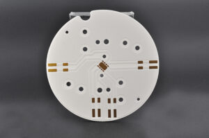
  5. Turn the trimmer slowly while watching the measurement.
  6. Stop when the reading enters the target range.
  7. Allow the circuit to stabilize and check the value again.
  8. Record or mark the setting when traceability is required.

If the reading moves in the wrong direction, first check the end-terminal connections and the test instruction. If the reading does not change, check whether the wiper is connected, whether the footprint matches the pinout, and whether the trimmer has reached an end stop.

Do not force the screw after the mechanism reaches the end of travel. If the target cannot be reached within the normal range, the problem may be the wrong resistance value, an incorrect surrounding component, excessive circuit tolerance, a wiring error, or a damaged trimmer.

Multiturn trimmers are useful when the final value is sensitive to small movement. Single-turn parts are faster when the acceptable range is broad. The correct choice makes calibration both repeatable and practical rather than merely possible.

trimmer potentiometer
A trimmer potentiometer is adjusted while the required circuit output is monitored.

Engineering Example: Verifying a Board-Mounted Trimmer Potentiometer Before PCBA Assembly

A low-volume LED tester project handled by EBest Circuit used a display connector close to a board-mounted trimmer potentiometer. Before assembling the five-board pilot lot, our engineering team needed to confirm that the trimmer would fit the PCB and remain accessible after assembly.

A BOM entry such as “10 kΩ trimmer” was not specific enough. Parts with the same resistance may have different pinouts, body sizes, and adjustment directions. A side-adjust trimmer, for example, could fit the PCB footprint but become blocked by the nearby display connector.

EBest Circuit compared the trimmer potentiometer datasheet with the PCB design and checked:

  • Pinout and lead spacing.
  • Body position and seated height.
  • Adjustment direction.
  • Connector clearance.
  • Screwdriver access.
  • Soldering compatibility.

The confirmed part number, orientation, and adjustment keepout could then be added to the assembly drawing. During functional testing, each board could be adjusted while the specified output was monitored.

This verification helped prevent footprint mismatches and inaccessible adjustment points before PCBA assembly. It also confirmed that the trimmer potentiometer would work as both an electrical component and an accessible calibration control.

FAQs About Trimmer Potentiometers

What does a trimmer potentiometer do?

It provides a small manual adjustment for resistance, voltage division, calibration, or threshold setting. The exact function depends on how the three terminals are connected in the circuit.

What is the difference between a trimmer potentiometer and a variable resistor?

A trimmer potentiometer is a physical component with three terminals. It can operate as a voltage divider using all three terminals or as a variable resistor using the wiper and one end terminal.

Which pin is the wiper on a trimmer potentiometer?

The wiper is often shown as terminal 2, but physical arrangements vary. Always confirm the exact datasheet drawing instead of assuming that the center physical pin is the wiper.

Is a multiturn trimmer better than a single-turn trimmer?

Not always. A multiturn trimmer provides finer adjustment but takes longer to set. A single-turn trimmer is faster but may be more sensitive. The better choice depends on the calibration tolerance and process.

Can a trimmer potentiometer be adjusted after conformal coating?

Only if the adjuster remains accessible and the coating process is compatible with the component. Specify a coating keepout or temporary mask when post-coating adjustment is required.

A suitable trimmer potentiometer should provide the required electrical range, fit the PCB footprint, remain accessible, and allow the circuit to be calibrated without excessive sensitivity. Check the exact datasheet, pinout, mounting style, adjustment direction, and operating limits before finalizing the part.

For PCB fabrication, component sourcing, PCBA, inspection, or customer-defined test support, send your files and requirements to EBest Circuit (Best Technology) at sales@bestpcbs.com.

You may also like

Resistor Tolerance: A PCB Buyer’s Guide to BOM Accuracy

August 24th, 2026

Resistor tolerance can determine whether a voltage divider, current-sense channel, or other precision circuit remains within its intended operating range. For PCB and PCBA buyers, the real risk is not only receiving the wrong nominal resistance; it is approving a component whose permitted variation, temperature behavior, or substitute specification exceeds the circuit’s error budget.

This guide helps you calculate the allowed resistance range, verify color bands and SMD ordering codes, review BOM and datasheet requirements, control substitutions, and define the inspection or test evidence needed before production. If you need support with BOM review, approved component sourcing, PCBA, inspection, or test coordination, contact EBest Circuit (Best Technology) at sales@bestpcbs.com.

resistor tolerance
Precision resistance measurement helps verify component identity and production requirements.

What Does Tolerance in Resistance Mean for PCB Buyers?

Tolerance in resistance is the permitted difference between a resistor’s nominal value and its actual resistance at the stated reference conditions. A 10 kOhm resistor with a tolerance of +/-1% is permitted to measure from 9.9 kOhm to 10.1 kOhm before other effects are considered.

That percentage is a manufacturing limit, not a promise that every part will be offset by the same amount. One production lot may cluster close to nominal, while another approved lot can sit elsewhere inside the specified band. A prototype measurement that happens to be near nominal does not justify replacing a 1% part with a 5% part.

For a buyer, tolerance should be treated as a controlled BOM characteristic alongside:

  • nominal resistance;
  • package and termination style;
  • rated power and working voltage;
  • temperature coefficient of resistance, usually stated in ppm/degree C;
  • pulse or overload capability;
  • technology, such as thick film, thin film, metal film, or wirewound;
  • qualification, environmental, and traceability requirements.

The percentage matters most when the circuit depends on the absolute resistance or on the ratio between multiple resistors. Examples include feedback networks, current sensing, gain setting, voltage dividers, reference paths, filters, timing networks, and bias circuits. It may matter less in a pull-up whose acceptable range is broad, but that conclusion must come from the circuit requirements rather than from a generic purchasing rule.

The useful procurement outcome is a BOM line that identifies the required tolerance unambiguously and an approved manufacturer part number whose datasheet confirms it.

How to Calculate Resistance Tolerance and Its Allowed Range

The basic calculation converts the tolerance percentage into an absolute deviation:

Allowed deviation = Nominal resistance x Tolerance percentage / 100

Minimum resistance = Nominal resistance – Allowed deviation

Maximum resistance = Nominal resistance + Allowed deviation

For a 4.7 kOhm resistor with +/-5% tolerance:

  • Allowed deviation = 4,700 Ohm x 5 / 100 = 235 Ohm
  • Minimum resistance = 4,700 Ohm – 235 Ohm = 4,465 Ohm
  • Maximum resistance = 4,700 Ohm + 235 Ohm = 4,935 Ohm

For the same nominal value at +/-1%, the permitted range becomes 4,653 Ohm to 4,747 Ohm. That narrower band may protect circuit performance, but it can also affect component cost, availability, technology choice, and the number of qualified substitutes.

Buyers should avoid using the nominal tolerance range as the entire error analysis. The delivered resistance can also shift with temperature, self-heating, aging, mounting stress, humidity, and measurement conditions. Contact resistance and fixture accuracy can distort low-ohmic measurements, while ordinary handheld instruments may not provide enough accuracy to accept or reject a tight-tolerance part.

Before turning the formula into an incoming-inspection limit, confirm:

  • the datasheet conditions under which initial tolerance is specified;
  • the measurement temperature and stabilization time;
  • whether lead or contact resistance must be compensated;
  • the required instrument accuracy and calibration status;
  • whether the customer’s acceptance limit includes guard banding;
  • whether the check is intended to verify identity, screen a lot, or prove circuit performance.

A calculated range is valuable because it exposes ambiguity early. It should not be mistaken for a complete reliability or functional-test specification.

resistor tolerance
A 100 Ohm resistor has a much narrower permitted range at ±1% than at ±5%.

Tolerance on Resistors: Color Bands and Letter Codes

Tolerance on resistors can be shown by color bands, printed letters, part-number suffixes, packaging labels, or manufacturer-specific ordering codes. The correct reading method depends on the resistor construction and the manufacturer’s documentation.

For common axial resistors, the separated tolerance band is often read after the significant-digit and multiplier bands. Frequently encountered colors include:

  • brown: +/-1%;
  • red: +/-2%;
  • green: +/-0.5%;
  • blue: +/-0.25%;
  • violet: +/-0.1%;
  • gray: +/-0.05%;
  • gold: +/-5%;
  • silver: +/-10%;
  • no tolerance band on some older three-band parts: typically +/-20%.

Letter codes are also common in ordering systems. Typical IEC-style tolerance letters include F for +/-1%, G for +/-2%, J for +/-5%, K for +/-10%, and M for +/-20%. Tighter classes can use letters such as B, C, or D, but the manufacturer’s datasheet and part-number structure remain the controlling evidence.

Color alone is not enough for production purchasing. Lighting, contamination, body color, band spacing, and human color perception can cause mistakes. A photograph of a loose component is weaker evidence than the original reel label, supplier certificate, manufacturer part number, and current datasheet revision.

Use markings as an identification check, then reconcile them with the controlled BOM and receiving records. If the marking conflicts with the label or datasheet, quarantine the material until the discrepancy is resolved. Do not instruct the assembly line to “use it because the measured value looks close.”

What Does 5% Tolerance on a Resistor Mean?

A 5% tolerance means the initial resistance may be as much as 5% above or below the nominal resistance at the specified reference conditions. It does not mean the resistor will drift by 5% during use, and it does not automatically mean the part has lower power capability or poorer reliability than a 1% resistor.

For example, a nominal 100 Ohm, +/-5% resistor can initially measure from 95 Ohm to 105 Ohm. A nominal 100 Ohm, +/-1% resistor has an initial range of 99 Ohm to 101 Ohm.

Whether 5% is acceptable depends on the circuit consequence at both limits. The engineering review should examine the worst-case output, not just the resistance difference. A wider tolerance can change:

  • divider voltage and threshold margin;
  • amplifier gain or filter response;
  • LED or bias current;
  • current-sense accuracy;
  • timing or oscillator behavior;
  • power dissipation in the resistor and connected parts;
  • production-test limits and false-failure rates.

A 1% part is not automatically sufficient for a precision function. Two nominally 1% resistors used as a ratio can create a larger worst-case ratio error if their deviations move in opposite directions. Matched networks or ratio-tolerance specifications may be more appropriate when tracking matters. Temperature coefficient and long-term stability can also dominate after the initial tolerance requirement is met.

The buyer’s decision should therefore be tied to the approved part number and circuit requirement. If a distributor proposes a 5% substitute for a 1% BOM line, similarity in nominal resistance and package does not make the substitution acceptable. Engineering approval is required before purchasing or assembly.

SMD Resistor Tolerance: What to Verify Beyond the Printed Code

SMD resistor tolerance is often difficult or impossible to confirm from the component body alone. Many chip resistors are too small to carry a complete marking, and some approved series are supplied unmarked. A three- or four-digit code usually identifies nominal resistance, not every electrical characteristic.

This makes reel-level and document-level control essential. Before releasing SMD resistors to a feeder, verify:

  • manufacturer name and complete manufacturer part number;
  • nominal resistance, tolerance, package, power rating, and series;
  • lot or date code and quantity;
  • supplier identity and traceability documents;
  • moisture or storage controls when applicable;
  • label consistency between outer packaging, reel, and receiving record;
  • current datasheet revision and ordering-code interpretation;
  • approved-source and approved-substitute status.

Do not infer tolerance solely from the number of printed digits. A four-digit marking is often associated with a more precise nominal value, but markings vary by manufacturer and package size. The complete ordering code is the safer control point.

Package selection also creates assembly risk. A replacement may share nominal resistance and tolerance yet have different rated power, working voltage, terminal material, thickness, land-pattern recommendation, pulse behavior, or anti-sulfur performance. These differences can affect solder-joint geometry, placement, inspection, field reliability, and compliance with the customer’s environment.

BestPCBS already provides separate guidance on SMD resistor package sizes. Use that dimensional information together with the selected manufacturer’s datasheet; do not treat the package code as a complete electrical specification.

How Resistor Tolerances Change Worst-Case Circuit Performance

Resistor tolerances change circuit results through both absolute-value error and ratio error. The relevant mechanism depends on the topology. Purchasing teams do not need to redesign the circuit, but they do need to recognize when a substitution requires engineering review.

Consider a simple divider with two equal nominal resistors. If the upper resistor moves to its maximum allowed value while the lower resistor moves to its minimum, the output ratio shifts in one direction. Reversing those deviations shifts it in the other direction. An analysis that assumes both resistors drift together can understate the worst case.

Similar interactions appear in:

  • operational-amplifier feedback networks, where resistor ratio sets gain;
  • shunt current measurement, where resistance error directly affects calculated current;
  • pull-up networks, where resistance interacts with leakage and capacitance;
  • RC timing and filtering, where both resistance and capacitance tolerances contribute;
  • bias networks, where current or operating point can move;
  • protection and threshold circuits, where margin may already be narrow.

Initial tolerance is only one contributor. A defensible review may also need temperature coefficient, ambient range, self-heating, long-term drift, voltage coefficient, board contamination, leakage, and the tolerances of other components. For low-resistance shunts, PCB copper and sensing geometry can be part of the measurement error. For high-resistance networks, surface leakage can become important.

The manufacturing handoff should translate the engineering conclusion into controlled fields: exact approved part numbers, explicit tolerance, no-substitute or approval rules, and any test limits. Without that translation, the error analysis can remain correct in the design file while procurement unintentionally releases a wider-tolerance part.

BOM and Datasheet Checks for the Correct Resistor Tolerance Value

The correct resistor tolerance value should appear consistently across the schematic, BOM, approved vendor list, purchase order, supplier quotation, and inspection plan. A mismatch between those files is a revision-control problem even if the material has not yet reached production.

Before requesting a PCBA quotation, provide a BOM that includes, at minimum:

  • unique item or reference designation;
  • nominal resistance with an unambiguous unit;
  • tolerance;
  • package or case size;
  • rated power and other critical ratings;
  • manufacturer and complete manufacturer part number;
  • approved alternatives or a clear no-substitution instruction;
  • applicable notes, standards, or traceability requirements;
  • BOM revision aligned with the released Gerber or ODB++ data, pick-and-place file, and assembly drawing.

Then review the datasheet for the exact ordering code. Family-level tables can contain multiple tolerance options, temperature coefficients, terminal finishes, and package ratings. A distributor title such as “10 kOhm chip resistor” is not enough to confirm the ordered variant.

Approved-substitute review should compare more than nominal value. Ask engineering to confirm tolerance, temperature coefficient, technology, rated power, working voltage, overload behavior, environmental options, dimensions, land pattern, availability, and any application-specific qualification. Record the approval against the exact substitute part number and applicable product revision.

EBest Circuit can flag BOM ambiguity, reconcile purchasing data with released files, and coordinate approved component sourcing. The customer should resolve circuit-performance questions and approve deviations before material is purchased or loaded for assembly.

How to Control Resistance Tolerance During Sourcing and PCBA

Resistance tolerance control begins before the purchase order. Inspection cannot recover a missing requirement that was never defined, and a functional test cannot always identify which BOM parameter caused a failure.

A practical control sequence is:

  1. Freeze the released BOM and identify tolerance-critical references.
  2. Confirm exact manufacturer part numbers and approved sources.
  3. Require documented approval before any substitution.
  4. Match purchase-order descriptions to the controlled BOM.
  5. Verify supplier, packaging, labels, lot information, and quantity at receiving.
  6. Perform risk-based identity or resistance checks with suitable calibrated equipment.
  7. Maintain reel-to-feeder and lot-to-build traceability where required.
  8. Verify first-article placement and polarity-independent component identity against the assembly data.
  9. Run the customer’s approved ICT, flying-probe, functional, or other test plan.
  10. Preserve inspection and test records with the production lot.

Measurement strategy should match the risk. Sampling resistance may help detect a wrong value or mixed lot, but it may not prove every part meets a tight tolerance. In-circuit measurements can be influenced by parallel paths. Functional testing can confirm product behavior at test conditions but may not demonstrate performance across temperature, input range, aging, or every component corner.

For a critical function, the customer may request additional evidence such as supplier certificates, incoming-inspection data, first-article records, AOI images, test logs, or serial/lot traceability. Each document answers a different question. A certificate supports identity or conformance; AOI supports placement and solder-joint inspection; resistance measurement supports the sampled electrical value; functional testing supports defined board behavior.

Agree on the evidence before production. Retrofitting traceability or reconstructing feeder history after a field complaint is slower, more expensive, and sometimes impossible.

Project Example: Controlling ±1% Printed Resistor Tolerance on a Ceramic PCB

In one anonymized EBest Circuit project, the resistors were printed directly onto a single-sided thick-film ceramic PCB.

Project specifications

  • 0.635 mm 96% alumina substrate
  • AgPd conductor with 20% palladium
  • Green solder mask with no legend
  • 12 boards per panel
  • Resistance values defined in the customer’s controlled table
  • COC and resistance test report required

Revision change

The A0 order included 24 boards plus five spares.

For B0, the board construction remained unchanged. However, the printed resistor tolerance was revised to +/-1%, and the order increased to 1,020 boards plus 12 spares.

The two versions looked similar, but their electrical acceptance limits were different.

Production control

EBest Circuit treated B0 as a new controlled revision. Each printed resistor had to remain within +/-1% of its specified nominal value.

Unlike an SMD resistor, a printed resistor has no reel label or separate manufacturer part number. Its resistance is a finished-board characteristic and must be measured.

Verification evidence

  • Visual inspection checked contamination, damaged edges, and printing defects.
  • Resistance measurement verified each printed resistor against its allowed range.
  • The resistance test report recorded the electrical results.
  • The COC confirmed overall order conformity.

Visual inspection could not replace resistance testing, and the COC could not replace measured data.

Project outcome

The B0 revision, +/-1% tolerance, 12-up panel format, and test documentation remained aligned as production increased from a small batch to more than 1,000 boards.

Buyer takeaway

When printed resistor tolerance changes, release a new drawing or product revision. Clearly define:

  • each nominal resistance;
  • its allowed tolerance;
  • measurement conditions;
  • inspection coverage;
  • test-report requirements.

A ceramic PCB can look identical to an earlier version and still be electrically nonconforming.

resistor tolerance
Printed resistors on a ceramic PCB require measured resistance evidence because they are finished-board characteristics.

FAQs About Resistor Tolerance

Is a 1% resistor always better than a 5% resistor?

No. A 1% resistor has a narrower initial resistance range, but the correct choice depends on circuit requirements, temperature behavior, rated power, pulse capability, cost, availability, and other specifications. Use the approved engineering requirement rather than a universal preference.

Does resistor tolerance include temperature drift?

Usually not. Initial tolerance and temperature coefficient are separate specifications. Temperature coefficient describes how resistance changes with temperature, while initial tolerance describes the permitted value at defined reference conditions. Check the exact datasheet.

Can incoming inspection prove that every resistor meets its tolerance?

Not automatically. The conclusion depends on sampling plan, instrument accuracy, measurement method, environmental conditions, and whether every part or only a sample is tested. Incoming inspection is often most useful for identity and gross-error detection unless a specific acceptance plan is defined.

Can a 5% resistor replace a 1% resistor if the measured sample is within 1%?

No automatic substitution should be made. A sample reading near nominal does not change the manufacturer’s tolerance specification for the lot. Obtain engineering approval for the exact proposed part before purchase or assembly.

What should I send for a resistor-critical PCBA quotation?

Send the released BOM with exact manufacturer part numbers, nominal values, resistor tolerance requirements, packages, ratings, approved alternatives, and revision status. Include assembly data, drawings, test requirements, and any traceability or inspection expectations. For BOM review, component sourcing, PCBA, and test coordination, contact EBest Circuit (Best Technology) at sales@bestpcbs.com.

You may also like

PCB Assembly France: Compare Suppliers and Get a Quote

August 24th, 2026

Choosing a supplier for PCB assembly France is not only a price decision. French engineers and buyers must protect design intent, component authenticity, build quality, delivery, and total landed cost—especially when comparing local, European, and overseas suppliers.

EBest Circuit (Best Technology) supports French PCB projects from its China-based PCB and PCBA factories. One commercial contact works with three engineers to coordinate DFM review, BOM optimization, PCB fabrication, component sourcing, assembly, inspection, and testing. The company supports prototypes and small batches as well as repeat production, including projects using heavy-copper, HDI, high-frequency, FPC, and rigid-flex PCB technologies.

Planning a PCB assembly project for France? Send your controlled PCB files, BOM, quantity, testing requirements, and delivery destination to sales@bestpcbs.com. EBest Circuit can review manufacturability and BOM risks before preparing an itemized quotation.

PCB assembly France
EBest Circuit’s SMT production environment supporting PCB assembly projects for French buyers.

What Should Buyers Expect from PCB Assembly France?

Expect a clearly defined manufacturing scope, named technical owners, controlled revisions, project-specific quality evidence, and a realistic landed delivery plan.

PCB assembly France” can describe three sourcing models: production in France, production elsewhere in Europe, or an overseas supplier serving French customers. The best fit depends on the project—not the search phrase.

Before comparing prices, confirm who owns each part of the work:

  • Bare PCB fabrication and electrical testing.
  • Component procurement and approved substitutions.
  • SMT, through-hole, and manual assembly.
  • Programming, inspection, and functional testing.
  • Packaging, freight, customs, and import documentation.

For prototypes, fast engineering feedback and revision control often matter more than a small unit-price difference. For repeat orders, component continuity, process stability, traceability, and change control become more important.

EBest Circuit is an overseas option for French buyers, not a French factory or local legal entity. Buyers should therefore include international freight, customs, import responsibility, time-zone communication, and total landed lead time in the comparison.

PCB Assembly in Europe vs China: Which Model Fits French Buyers?

European production may fit projects that need frequent site access or very short transport. China-based production may fit projects that benefit from integrated PCB, component, assembly, and testing resources.

Buyer priorityEurope may fit whenChina may fit when
Engineering accessFrequent site visits are essentialOnline engineering reviews are sufficient
Supply scopeParts and processes are already localPCB, sourcing, PCBA, and test need coordination
CostProximity outweighs unit costRepeat-volume economics matter
Quality oversightOn-site review is preferredRemote records and traceability are accepted
DeliveryTransport time is the main constraintBuild time and sourcing efficiency matter more

Choose a nearby supplier when the design changes daily, physical collaboration is essential, or transport time dominates the schedule.

Consider a qualified China-based supplier when files are sufficiently mature, one team must coordinate several supply stages, or the project requires wider component-sourcing options. A hybrid model is also possible: keep unstable early builds close to the design team, then transfer a controlled package for repeat production.

In every model, compare the time from data release to usable boards at your facility—not only the factory build time.

PCB assembly France
Automated component placement on assembled PCBs during PCBA production.

What Files Are Needed for a PCB Assembly France Quote?

Send one revision-matched manufacturing package. Gerber files and a basic BOM are rarely enough for an accurate, production-ready quote.

Your package should include:

  • PCB data: Gerber or ODB++, drill files, board outline, stack-up, material, copper weight, finish, impedance, and special-process notes.
  • BOM: Manufacturer part numbers, quantities, reference designators, do-not-fit positions, approved alternates, and buyer-supplied parts.
  • Assembly data: Pick-and-place coordinates, rotations, board side, polarity, connector orientation, and assembly drawings.
  • Programming data: Firmware version, programming method, and verification instructions.
  • Quality requirements: IPC class if applicable, SPI, AOI, X-ray, electrical or functional test, report format, and acceptance limits.
  • Delivery requirements: Quantity, panelization preference, packaging, labeling, traceability, Incoterm, and destination.

Use the same revision identifier across every file. If the PCB data, BOM, centroid file, firmware, and drawings do not match, the supplier should issue an engineering query rather than guess.

EBest Circuit can provide a DFM pre-review and BOM risk or optimization list. The review may identify footprint conflicts, polarity questions, stencil risks, inaccessible test points, obsolete parts, long-lead components, and possible alternates. No substitute should be purchased without the buyer’s approval.

Before requesting a final price: Email the release package to sales@bestpcbs.com and ask EBest Circuit to separate confirmed parts, proposed alternates, unavailable items, tooling, testing, freight, and other one-time charges.

How Should French Buyers Compare PCB Assembly Quotes?

Compare equivalent scope and total landed project cost—not only the quoted price per assembled board.

Check these six areas in every quotation:

  • Bare PCB: Material, stack-up, finish, impedance, panelization, tooling, electrical test, and quantity.
  • Components: Exact part numbers, approved alternates, minimum purchasing quantities, excess material, and buyer-supplied parts.
  • Assembly: SMT sides, through-hole work, manual operations, stencil, setup, programming, and rework assumptions.
  • Quality: First-article approval, SPI, AOI, X-ray, functional testing, reports, and failure handling.
  • Delivery: Lead-time start point, production stages, freight method, customs, duties, VAT, and destination.
  • Records: Lot traceability, certificate of conformity, material records, and retention period.

Calculate the full project cost:

PCB + components + assembly + tooling + programming + testing + packaging + freight + import costs + expected delay or rework risk

Ask when the lead-time clock starts. It may begin after payment, after engineering questions close, or after all components arrive—not when the purchase order is sent.

Also evaluate the quality of the supplier’s response. A team that finds an incorrect footprint, unclear polarity, or risky substitute before production may save more than a small unit-price discount.

Which Quality Checks Matter for PCB Assembly France?

Use inspections that match the assembly risk, then request records that show what was checked, when it was checked, and how failures were handled.

Before production, confirm:

  • DFM and BOM review.
  • Incoming component and moisture-control procedures.
  • Stencil design and first-article approval.
  • Firmware, test limits, and fixture responsibility.

During SMT, 3D solder paste inspection can measure paste volume, area, and height before components are placed. At EBest Circuit, our 3D SPI capability supports 01005-class components. Our engineers confirm its suitability against the actual pad, stencil, package, and process design before production.

Placement controls should cover feeder setup, polarity, program approval, and first-piece verification. For reflow, EBest Circuit profiles new products using a physical board and retains process records. Buyers can request the project-specific thermal-profile evidence required by their quality plan.

After reflow, use the appropriate inspection method:

  • 3D AOI: Missing, wrong, rotated, reversed, lifted, bridged, tombstoned, or visibly under-soldered components.
  • X-ray: Hidden BGA, CSP, flip-chip, and similar joints.
  • Electrical or functional test: Circuit operation, firmware, interfaces, limits, and pass/fail results.

AOI and X-ray do not prove that a circuit functions. A complete test plan must define coverage, acceptance limits, records, and failed-unit disposition.

For medical, industrial-control, automotive-electronics, communications or 5G, and AI-hardware projects, verify that the factory, certification scope, inspection plan, and product controls match the actual application. Industry experience supports better engineering questions; it does not replace product-specific validation or the buyer’s regulatory responsibility.

PCB assembly France
A powered multi-unit test setup used to support repeatable PCBA verification.

What Drives the Cost of Small Batch PCB Assembly in France?

Small-batch unit prices are driven by fixed engineering, setup, tooling, and test costs spread across fewer boards.

The largest cost drivers are:

  • PCB technology: Layers, material, copper weight, impedance, finish, vias, thickness, tolerances, and panel utilization.
  • Components: Price, shortages, minimum order quantities, lifecycle risk, alternates, and special handling.
  • Assembly: Placement count, package mix, board sides, fine-pitch devices, through-hole work, hand soldering, cleaning, coating, and mechanical assembly.
  • One-time work: DFM, stencil, programming, fixtures, first-article inspection, and test development.
  • Evidence: X-ray coverage, test time, serialization, traceability, and report requirements.
  • Schedule: Expedited material, priority production, express freight, customs, and delivery destination.

Buyers can reduce unnecessary cost by allowing the supplier to optimize panelization, resolving BOM risks before purchasing, approving alternates early, and reusing validated tooling when the revision permits. Do not remove an essential inspection or test simply to lower the quote.

EBest Circuit supports prototypes and small batches and offers an approximately 1.5-week rapid PCBA delivery target for suitable projects. This is a project-specific target, not a blanket guarantee. File readiness, component availability, PCB technology, test fixtures, factory capacity, freight, and customs all affect the actual delivery date.

How Should French Buyers Qualify an Overseas PCB Assembly Supplier?

Convert every important supplier claim into a document, record, sample, audit check, or pilot-build result.

Request the following evidence:

  • Legal company and manufacturing-site details.
  • Current certificates and their covered locations and scopes.
  • A sample DFM report and BOM risk or optimization list.
  • First-article, inspection, traceability, and nonconformance records.
  • Equipment capability matched to your board—not a generic machine list.
  • ESD, moisture, counterfeit-avoidance, calibration, and maintenance controls.
  • Named owners for engineering, sourcing, quality, and schedule escalation.

EBest Circuit holds ISO 9001, ISO 13485, IATF 16949, and AS9100D certifications. For a regulated project, ask us for the current certificate, covered manufacturing site, and applicable scope so your quality team can confirm that it matches the project requirements.

Our service model assigns one commercial contact supported by three engineers. DFM analysis, BOM optimization, and process recommendations are supported by team members with approximately 20 years of PCB, PCBA, and R&D experience. French buyers receive specific, documented engineering questions that are reviewed and closed before production.

EBest Circuit operates its own PCB and PCBA factories and works with more than 1,000 supply-chain partners. For each project, we can clarify which factory and approved supplier will handle every critical process or component, as well as how approved vendors and remaining materials are controlled.

For repeat production, test traceability during the pilot. Our digital workshop can retrieve material batch, product batch, production cycle, and progress information within five seconds. Select one serial or lot number, and our team can retrieve its related material, process, inspection, and shipment records for review.

PCB Assembly France Project Example: Prototype to Repeat Production

This anonymized example is based on a European customer project supported by EBest Circuit, showing how our engineering team clarified one unresolved requirement before material release and helped establish a controlled manufacturing package for repeat orders.

The project covered 30 assembled units using a three-layer flexible PCB. Recorded requirements included:

  • 12 µm base copper with additional plating.
  • Adhesive-free polyimide constructions.
  • Finished thickness of 0.20 mm ±0.03 mm.
  • ENIG and 50-ohm controlled impedance.
  • FR-4 stiffening below the component area.
  • Polyimide stiffening below the gold fingers.
  • EMI shielding film on both sides.
  • Components sourced by EBest Circuit.
  • Supplier-designed production panelization.

A 0.2–0.4 mm adhesive-tape requirement still needed clarification. The engineering query had to confirm its location, finished thickness, adhesive type, drawing reference, temperature exposure, and assembly sequence. Guessing could have affected fabrication, assembly, or the final mechanical fit.

Before moving from prototype to repeat production, the buyer and supplier should freeze:

  • PCB stack-up, impedance, finish, stiffeners, shielding, adhesive locations, and panel drawing.
  • BOM revision, purchased parts, approved alternates, and excess-material disposition.
  • Centroid data, orientations, stencil, work instructions, solder paste, reflow profile, and support tooling.
  • SPI, AOI, X-ray, dimensional, electrical, and functional-test requirements.
  • Engineering queries, deviations, repairs, and design corrections from the pilot.
  • Sample acceptance criteria and authorization to release the repeat order.

The customer benefit is controlled transfer. Repeat production uses one approved manufacturing package instead of relying on memory, email fragments, or an uncontrolled copy of the prototype files.

PCB assembly France
A repeat-unit validation setup illustrating the transition from prototypes to controlled production.

PCB Assembly France FAQs

Does EBest Circuit have a PCB assembly factory in France?

No. EBest Circuit (Best Technology) manufactures in China and serves French and other international customers. Buyers should include freight, customs, import responsibility, communication, and total landed lead time when comparing it with local or European suppliers.

What files should I send for a PCB assembly quote?

Send revision-matched PCB fabrication data, drill files, stack-up, BOM, centroid data, assembly drawings, programming files, test requirements, quantity, panelization instructions, packaging requirements, and delivery destination.

Can EBest Circuit support prototypes and small-batch PCBA?

Yes. EBest Circuit supports prototypes and small batches and can coordinate PCB fabrication, component sourcing, PCBA, inspection, and testing. Provide the expected repeat-production path so tooling, material, and quality controls can be planned from the start.

Can a PCBA order be delivered in 1.5 weeks?

Approximately 1.5 weeks is a rapid-delivery target for suitable projects, not a guaranteed lead time for every order. It depends on file readiness, component availability, PCB technology, engineering-query closure, testing, capacity, freight, and customs.

Which inspection reports should a French buyer request?

Request evidence matched to the project risk: DFM and BOM review records, first-article approval, SPI and AOI results, X-ray for hidden joints where applicable, reflow-profile evidence, functional-test results, lot traceability, and a certificate of conformity when contractually required.

Ready to review your PCB assembly project for France? Send your Gerber or ODB++ files, BOM, centroid data, assembly drawings, quantity, test requirements, and delivery destination to sales@bestpcbs.com. EBest Circuit (Best Technology) can provide a DFM pre-review, BOM risk and optimization list, recommended inspection plan, and an itemized PCB assembly quotation.

You may also like

PCB Microsection Analysis: How Cross-Section Testing Finds Hidden Defects

August 21st, 2026
PCB microsection analysis laboratory with microscope and plated through-hole cross section
PCB microsection analysis exposes internal structures that external inspection cannot see.

PCB microsection analysis is a destructive inspection method that cuts through a board or test coupon, mounts the sample, grinds and polishes it, then examines the exposed structure under a microscope. It can show plating distribution, via-wall cracks, inner-layer connections, registration, laminate condition and other internal features that remain hidden during ordinary visual inspection.

The method is powerful, but a polished image alone is not a verdict. A useful result depends on representative sampling, correct preparation, a known inspection plane and acceptance criteria tied to the applicable drawing, procurement specification and product class. This guide explains how to plan the analysis, read the evidence and turn the report into a manufacturing decision.

What PCB Microsection Analysis Actually Shows

A microsection provides a direct two-dimensional view through selected internal PCB features. It is commonly used to evaluate plated through-holes, blind or buried vias, copper interfaces, laminate layers and selected solder joints. Because the sample is physically cut, the analyst can inspect material boundaries rather than infer them from an external image.

The method is especially useful when the question is structural: Is the hole wall continuous? Does the plated copper connect cleanly to the inner layer? Is there evidence of resin recession, separation, cracking or voiding? Are layers aligned around the inspected feature? These questions are different from verifying the electrical netlist, so microsection results should complement—not replace—appropriate electrical and functional tests.

Feature What the section can reveal Decision supported
Plated hole or via barrel Continuity, local thin areas, cracks, nodules or voids Plating-process and thermal-reliability review
Inner-layer connection Land contact, resin smear evidence, separation or breakout Drilling, desmear and registration review
Multilayer stack Layer position, dielectric condition and local registration Lamination and imaging-process review
Surface and hole finish Local layer interfaces and coating condition Finish-process investigation
Solder joint Internal wetting profile, voids, cracks and interface condition Assembly failure analysis

When a Microsection Is Worth the Destructive Sample

Use microsectioning when direct internal evidence is more valuable than preserving the selected sample. Good triggers include process qualification, lot acceptance required by contract, investigation of a suspected via or interconnect failure, validation after thermal stress, and confirmation that a corrective action changed the internal result.

Do not order a section merely because it appears thorough. Start with the failure question. If the issue is an open circuit, an electrical test can locate the affected net before cutting. If the concern is a hidden BGA solder joint, X-ray may narrow the location. If the concern is hole-wall plating or an inner-layer interface, cross-sectioning may provide the decisive evidence.

For an overview of where microsection preparation sits among other procedures, review the IPC-TM-650 PCB test methods guide. The applicable test method defines preparation or measurement practice; the purchase drawing and product specification still need to define what is acceptable for the actual board.

Coupon or Production Board: Choose the Sample Before Cutting

The sample must represent the process and the feature under investigation, or the microscope image can answer the wrong question with great precision. A production coupon avoids sacrificing a sellable board and can be designed around representative holes, traces and layer relationships. A failed production board may be necessary when the investigation concerns one specific field failure or localized anomaly.

Record the panel position, lot, board revision, coupon identity, target hole or via, prior thermal exposure and cutting orientation before preparation. For intermittent failures, first preserve photographs and electrical evidence. Once the sample is cut and polished, the original condition cannot be reconstructed.

  • Use a defined coupon when the goal is routine process monitoring or contractual conformance.
  • Use the affected board when location-specific evidence is essential and the sample can be sacrificed.
  • Use more than one location when the suspected problem could vary across a panel or stackup.
  • Keep an unsectioned control sample when comparison may be needed later.

How the Microsection Preparation Process Works

The usual sequence is target selection, sample removal, mounting, controlled grinding, fine polishing, optional micro-etching and microscopic examination. Each step can change the surface, which is why preparation quality must be checked before interpreting a defect.

  1. Define the target plane. Mark the exact hole, via, interface or joint and the direction of the intended cut.
  2. Remove the specimen. Leave enough material around the target to avoid mechanical damage at the feature of interest.
  3. Mount the sample. Encapsulate and support the specimen so dissimilar materials remain stable during grinding.
  4. Approach the target gradually. Coarse removal gets near the inspection plane; finer abrasives reduce deformation and deep scratches.
  5. Polish the exposed face. The final surface must be clear enough to distinguish copper, resin, glass reinforcement and interfaces.
  6. Apply micro-etch only when justified. Etching can improve contrast, but excessive etching may alter the apparent boundary.
  7. Capture calibrated images. Record magnification, scale, target identity and measurement locations.

IPC-9241 discusses variables and problems across this preparation chain. It is a valuable process reference, but it does not eliminate the need for a product-specific acceptance plan.

What to Measure Around Plated Through-Holes and Vias

Measure the features that connect directly to the suspected risk, not every visible dimension by habit. For plated holes and vias, the inspection plan may include local copper distribution, barrel condition, the inner-layer connection, annular relationship, dielectric separation and evidence of cracking or voiding.

Measurements must identify where they were taken. A single favorable point can hide a local thin area, while an off-center section can make the geometry look misleading. The report should show the complete inspected feature plus higher-magnification images of relevant interfaces.

Annular geometry is easier to interpret when the design intent is already understood. The related guide on annular rings in PCB design explains the relationship between the finished hole, pad and registration allowance.

How Microsections Reveal Lamination and Registration Problems

A well-targeted section can show whether internal layers and dielectric interfaces are positioned and bonded as expected at that location. The analyst may see local layer shift, uneven dielectric spacing, separation, resin-rich or resin-starved areas, disturbed glass bundles or damage near drilled features.

Interpret these observations in context. A cross-section is a narrow plane through a three-dimensional product. One local observation does not automatically describe the entire panel, and a visual difference is not automatically a reject. Correlate the image with panel position, stackup, drilling route, lamination history and the specified acceptance criteria.

HDI constructions deserve special attention because sequential lamination and microvia structures create multiple interfaces. For a wider process view, see the HDI PCB manufacturing process guide.

Which Defects Are Real and Which Are Preparation Artifacts

Scratches, edge rounding, copper smearing, pull-out, excessive etch and a section that misses the target center can imitate or conceal real defects. Before declaring a crack or void, check whether the feature continues consistently, whether adjacent material is distorted and whether a second preparation or viewing condition confirms it.

Illustrative PCB cross section showing a barrel crack and plating void for microsection defect review
Illustrative cross-section: suspicious features should be confirmed against preparation quality and the applicable acceptance criteria.

A disciplined report separates three statements: what is visibly observed, what criterion applies and what root-cause hypothesis remains to be tested. For example, “a discontinuity is visible at the knee” is an observation. “The feature does not meet drawing requirement X” is an acceptance conclusion. “Thermal stress caused the discontinuity” is a causal hypothesis that may require history, replication or additional analysis.

Microsection vs X-Ray, AOI and Electrical Test

No single inspection method covers all PCB risks; choose the method according to the physical question. Cross-sectioning gives direct material and interface evidence at one destroyed location. X-ray shows density and geometry without cutting. AOI evaluates visible surfaces. Electrical test verifies connectivity and isolation but does not explain every structural cause.

Method Best question Main limitation
Microsection What is happening inside this material interface? Destructive and highly location-dependent
X-ray Is hidden geometry, voiding or alignment suspicious? Overlapping features and material density can limit interpretation
AOI / visual inspection Are visible surfaces, patterns or components acceptable? Cannot directly see most internal interfaces
Electrical test Are intended connections present and unintended connections absent? May not reveal a structurally weak connection that still conducts
Functional test Does the assembled product perform its intended function? May locate the symptom without isolating the physical cause

A broader method-selection comparison is available in the PCB testing methods and equipment guide.

How to Read a PCB Microsection Report

A decision-ready report must connect every image and measurement to a traceable sample, target feature and acceptance requirement. Attractive microscope photographs without identification, scale or disposition are not enough for lot release or corrective action.

  • Confirm the purchase order, board number, revision, lot and sample identity.
  • Verify whether the sample is a coupon or production board and where it came from on the panel.
  • Check preparation orientation and whether the inspected plane passes through the intended feature.
  • Require a scale bar or calibrated measurement reference on measurement images.
  • Match each reported value to a clearly marked location.
  • Separate observations from acceptance decisions and root-cause hypotheses.
  • Identify the drawing, specification revision and product class used for disposition.
  • Record whether thermal conditioning or other preconditioning occurred before sectioning.
  • Ask for a clear Pass, Fail or Engineering Review disposition with the reason.

How to Write Acceptance Criteria Into the PO and Quality Plan

Specify the governing documents, product class, coupon plan, sampling trigger, inspected features and required report content before fabrication starts. A late request for “a microsection report” can produce images that do not answer the buyer’s actual reliability concern.

Do not copy a generic numerical limit into every project. Acceptance depends on board technology, applicable IPC performance specification, customer drawing, qualification status and contract. State which document controls if requirements conflict. Also define whether a failed coupon stops the lot, triggers additional samples or requires an engineering review.

A practical PO note can request: board and lot traceability; coupon identity and panel location; specified preconditioning; defined inspection features; calibrated images; the applicable requirement beside each result; and retention of the report for an agreed period.

What to Send for a Failure-Analysis Review

Send enough evidence to preserve the failure context before anyone chooses the cut location. The most useful package includes the board revision, Gerber or ODB++ data, stackup, fabrication notes, drill information, affected net or component, symptoms, electrical measurements, thermal history, lot data and marked photographs of the suspect location.

If assembly is involved, add the BOM, CPL, assembly drawing, reflow history when available and the exact point at which the failure appeared. State whether the goal is conformance verification, root-cause investigation or process comparison; each goal may require a different sample plan.

Never cut the only failed sample before documenting it. When the defect may be intermittent, preserve electrical behavior and external condition first. The sectioning plan should be approved by the person responsible for the investigation.

How Microsection Findings Should Change Production Controls

The value of microsection analysis comes from the control change it supports, not from the microscope image itself. A confirmed issue should be traced to the relevant process window—such as drilling, desmear, plating, lamination, imaging, thermal exposure or assembly—and linked to containment, root-cause verification and corrective action.

For recurring production, compare like-for-like evidence: the same coupon design, target feature, preparation orientation, measurement definition and acceptance rule. Otherwise, apparent improvement may be caused by a changed inspection method rather than a changed process.

  1. Contain suspect lots and protect traceability.
  2. Confirm the observation with suitable repeat evidence.
  3. Identify the process variable capable of producing that structure.
  4. Change and document the control or process window.
  5. Verify effectiveness with new representative samples.
  6. Update the control plan, work instruction or supplier requirement.

FAQ About PCB Microsection Analysis

Is PCB microsection analysis destructive?

Yes. The selected coupon or board area is cut, mounted, ground and polished. Use a production coupon when possible, and document any unique failed sample before sectioning because the original condition cannot be restored.

Is microsectioning the same as cross-section analysis?

In PCB work, the terms are commonly used for the same preparation-and-inspection approach. “Microsectioning” emphasizes specimen preparation, while “cross-section analysis” emphasizes examination and measurement of the exposed plane.

Can a microsection prove that the whole PCB lot is good?

Not by itself. It directly represents the inspected sample and plane. Lot conclusions require an agreed coupon design, sampling plan, panel-location logic and acceptance rule that make the evidence representative.

Can X-ray replace PCB microsection analysis?

Not for every question. X-ray is non-destructive and useful for hidden geometry and density differences, while a microsection directly exposes material interfaces. The two methods often complement each other during failure analysis.

What standards are commonly associated with PCB microsections?

IPC-9241 addresses microsection preparation guidance, and IPC-TM-650 includes relevant preparation and dimensional inspection methods. Product acceptance normally comes from the applicable performance specification, acceptability standard, drawing and purchase requirements.

Should a coupon be thermally stressed before sectioning?

Only when the qualification or investigation plan requires it. Preconditioning can expose weaknesses that are not visible in an as-received sample, but the condition, cycle and sequence must be recorded so results remain interpretable.

What makes a microsection report traceable?

It should identify the board, revision, lot, coupon or sample, panel location when relevant, target feature, preparation orientation, image scale, measurement locations, governing requirements and final disposition.

Why can two laboratories report different measurements?

Differences may come from sample position, section plane, edge preparation, calibration, measurement definition or interpretation. A shared method, marked measurement locations and retained images make comparisons more reliable.

How do I avoid confusing an artifact with a real crack?

Check preparation quality, nearby material deformation and whether the feature persists under another viewing condition or repeat section. A real defect conclusion should not rely on one ambiguous image.

What files should accompany an RFQ that needs microsection evidence?

Send Gerber or ODB++, stackup, drill data, fabrication drawing, board class or performance requirement, coupon or sampling expectations, required preconditioning, inspection features, report format, quantity and target schedule.

Turn the Cross-Section Into a Clear Manufacturing Decision

A good microsection plan starts before cutting: define the risk, choose a representative target, control preparation and connect every observation to an agreed acceptance rule. That discipline prevents both false rejects and false confidence.

Need a PCB or PCBA quotation with defined cross-section evidence? Send EBest Circuit your Gerber or ODB++ files, stackup, drill data, quantities, product class, coupon or sampling expectation, preconditioning requirement and target delivery date. Our engineering team can review the manufacturing package and clarify which inspection evidence should be included before production. Email sales@bestpcbs.com to request a DFM and quality-plan review.

You may also like

Enclosure Case Aluminum PCB: Design, Thermal and Assembly Guide

August 21st, 2026

An enclosure case aluminum pcb project combines a printed circuit board or PCBA with an aluminum housing that provides mechanical protection, connector access, heat spreading and electromagnetic shielding. Reliable integration depends on more than selecting a box that appears large enough. The PCB outline, mounting system, component height, panel cutouts, grounding points, thermal interfaces and manufacturing tolerances must be developed as one assembly.

Enclosure case aluminum PCB assembly in an extruded aluminum electronics housing

What Does Enclosure Case Aluminum PCB Mean?

The phrase normally describes a PCB installed in an aluminum electronics enclosure. The enclosure may be an extruded profile with internal card guides, a two-piece die-cast box, a folded sheet-metal housing or a machined aluminum body. The circuit board can be standard FR4, high-Tg FR4, an RF laminate, a metal-core board or another construction selected for the electrical and thermal load.

The enclosure and PCB have separate manufacturing data. PCB files define copper, drill, solder mask, board outline and assembly details. Enclosure drawings define cavity dimensions, wall thickness, rails, bosses, threaded holes, panel cutouts, surface finish and sealing features. A single mechanical datum scheme must relate the two data sets so that a connector, switch or indicator lands in the intended panel opening after all tolerances are applied.

How Is an Aluminum Enclosure Different from an Aluminum PCB?

An aluminum enclosure is a mechanical housing. An aluminum PCB is a circuit substrate, usually an insulated metal substrate with a copper circuit layer, dielectric layer and aluminum base. Either one can exist without the other: a conventional FR4 control board can sit inside an aluminum case, while an aluminum PCB can be mounted in a polymer housing.

Item Primary function Design-controlled features
Aluminum enclosure Protection, structure, shielding and possible heat spreading Internal cavity, rails, bosses, panel openings, seals and finish
Aluminum PCB or MCPCB Electrical interconnection with a thermally conductive metal base Circuit pattern, dielectric, metal base, board thickness and surface finish
FR4 PCB in an aluminum case General signal, control and power circuitry inside a conductive housing Stack-up, mounting, clearance, grounding and connector alignment

When heat must pass from components through the circuit board to the housing, a metal-core PCB can reduce part of the thermal path. It does not eliminate the need to calculate interface resistance, contact pressure and the enclosure-to-ambient path.

Which Aluminum Enclosure Type Fits a PCB Assembly?

The enclosure type should follow the required production volume, environmental protection, machining burden, thermal path and service method. An extruded aluminum case is practical for rectangular electronics because the profile can include PCB rails and only the end plates require most connector openings. Die-cast cases provide robust walls and sealing options, but their draft angles and internal radii reduce usable cavity space. Sheet-metal housings are efficient for larger or lower-profile equipment and permit formed brackets, although bend tolerances must be included in the stack-up.

Extruded die-cast and sheet aluminum enclosure types for PCB assemblies
Enclosure type Best fit PCB integration concern
Extruded profile Controllers, instruments and power modules with a consistent cross-section Rail width, board insertion path and end-panel connector alignment
Die-cast box Rugged or sealed assemblies with moderate production volume Boss locations, corner radii, draft and conductive finish at grounding points
Sheet aluminum Larger chassis, rack equipment and low-profile electronics Bend tolerance, PEM hardware, panel flex and cable routing
Machined enclosure Low-volume precision, RF or specialized thermal assemblies Cost, datum control and avoidance of unnecessary machining detail

A sealed housing also needs a pressure and moisture strategy. Gaskets, cable glands and vents affect available panel space, while trapped heat can make an enclosure with a high IP rating run hotter than an open laboratory prototype.

How Should the PCB Outline and Internal Rails Be Matched?

For a rail-mounted board, specify the finished PCB thickness together with the rail slot width and positional tolerance. Nominal 1.6 mm FR4 is not an exact dimension; copper, laminate, solder mask and fabrication tolerance influence the finished thickness. The rail must provide insertion clearance without allowing enough lateral movement to misalign connectors or create vibration wear.

The enclosure drawing should state the usable rail depth, entry chamfer, internal corner radius and obstruction-free insertion path. The PCB drawing should state the finished outline tolerance, board thickness tolerance and any edge bevel. Keep copper, plated features and fragile components away from sliding edges. If the board enters at an angle before seating, model the swept volume rather than checking only the final position.

Card-edge grounding requires a separate decision. A bare copper or plated edge contact can provide controlled chassis connection, while solder mask on the rail edge prevents an unintended electrical path. Anodized aluminum is electrically insulating at the surface, so apparent metal-to-metal contact should never be assumed to be a reliable ground.

How Should Mounting Holes, Standoffs and Keepouts Be Designed?

Standoff locations should restrain the PCB without bending it during screw installation, connector mating or cable handling. Place support near high insertion-force connectors and heavy components, but maintain access for drivers and inspection. Three well-positioned supports define a plane; additional standoffs require tighter coplanarity control to avoid forcing a warped board against the enclosure.

PCB rails standoffs mounting holes keepouts and panel cutout alignment
  • Size non-plated mounting holes for screw clearance plus PCB and enclosure positional tolerance.
  • Use plated mounting holes only when the electrical connection is intentional and the current path is defined.
  • Keep copper, vias and components outside washer, screw-head and standoff contact zones.
  • Check underside lead protrusion against the standoff height and enclosure floor.
  • Define whether insulating washers, shoulder bushings or nylon hardware are required.
  • Reserve tool access so the assembly sequence does not depend on an angled or partially engaged screw.

A mounting-hole keepout is not only a circle around the drill. It must cover screw-head sweep, washer diameter, driver access, possible standoff misalignment and any conductive debris created during service.

How Do Connectors and Panel Cutouts Affect PCB Layout?

Panel-mounted connectors establish some of the most important PCB datums. Define the connector mating face, centerline and height from the same enclosure reference used for the cutout. The footprint courtyard alone may not include shell tabs, latch motion, cable overmold or the hand clearance needed to mate the connector.

Allow for PCB positional tolerance, connector placement tolerance, reflow movement and panel machining tolerance. A cutout should clear the connector body without becoming so large that it weakens the panel, exposes internal circuitry or defeats an EMI gasket. For USB, RJ45, D-sub, circular and terminal-block interfaces, check the actual production part rather than relying on a generic model.

Front-panel LEDs and light pipes require optical alignment as well as mechanical clearance. Switches need travel clearance and force transfer without flexing the PCB. If a connector is mechanically fixed to the panel and soldered to the board, avoid a fully constrained geometry that transfers panel tolerance directly into solder joints.

How Does an Aluminum Case Change PCB Thermal Design?

Aluminum spreads heat well, but the housing becomes useful only when a controlled path connects the heat source to it. The complete path may include the component junction, package, solder joint, PCB copper, thermal vias or metal core, thermal interface material, enclosure wall and external convection. The largest temperature drop can occur across a thin-looking interface if contact area or pressure is poor.

Thermal path from power component through PCB and interface pad to aluminum enclosure

Begin with the allowable component junction temperature and ambient range, then allocate thermal resistance across the path. Use interface pads only where compression is controlled; an excessively thick pad accommodates tolerance but increases thermal resistance. Avoid routing high-current or temperature-sensitive circuits through a clamping zone without evaluating mechanical stress.

For a standard FR4 PCB, copper planes and thermal vias can move heat toward a chassis contact area. Higher heat flux may justify MCPCB, a local copper coin, a bonded heat spreader or direct component-to-housing contact. The correct choice follows heat density and electrical isolation requirements, not the presence of an aluminum case alone.

How Should Grounding and EMI Shielding Be Planned?

A conductive enclosure can reduce radiated emissions and improve immunity, but seams, apertures, cable shields and poorly controlled contacts can dominate performance. Decide where circuit ground connects to chassis, whether the connection is direct or capacitive, and whether one point or multiple low-inductance points are required by the frequency range.

Remove or mask anodizing at designated bonding locations, then use compatible hardware and controlled contact pressure. Star washers can penetrate surface films but may damage finishes and create debris; conductive gaskets or plated bonding pads provide more repeatable high-frequency contact when designed correctly. Keep the chassis connection short and wide because a long trace or wire adds inductance.

Connector shields should usually meet the enclosure at the entry point rather than carrying high-frequency current across the PCB before reaching chassis. Panel gaps, ventilation slots and display windows must be evaluated against the relevant wavelength and immunity environment. Verify the completed assembly, because a bare-board EMC test cannot represent enclosure seams and cable exits.

How Can Galvanic Corrosion and Electrical Shorts Be Prevented?

Aluminum, copper, nickel-plated parts and steel fasteners can form galvanic couples when moisture and an electrical path are present. Material pairing, surface finish, sealing and drainage should be chosen for the expected environment. Do not remove anodizing over a broad area merely to obtain ground; create small, controlled bonding points and protect the surrounding surface.

Electrical insulation needs positive dimensions. Maintain clearance between exposed conductors and the enclosure under the worst PCB position, board bow and hardware tolerance. Add insulating films, shoulder washers or barriers where a single shifted board could contact metal. Confirm that solder tails, clipped leads and through-hole pins cannot reach the enclosure floor after assembly.

Service operations also matter. Loose screws, metal chips from field drilling and damaged insulating pads can create faults after the product passed factory test. Captive hardware, deburring, cleaning and clear replacement-part control reduce these risks.

Which Tolerances Must Be Controlled Between PCB and Enclosure?

PCB-to-enclosure fit is a tolerance-chain problem. Choose a primary datum, usually a mounting feature or panel reference, and calculate the extreme position of each critical feature from that datum. Do not independently dimension every feature from different enclosure edges; accumulated ambiguity makes inspection and troubleshooting difficult.

Critical relationship Contributors to the tolerance chain Practical control
Connector to panel opening PCB outline, hole position, standoff, connector placement and cutout position Common datum plus verified production connector model
PCB edge to rail Finished board width, thickness, rail width, extrusion straightness and finish Rail-fit coupon or first-article insertion test
Component to lid Component height, solder stand-off, board bow, standoff height and lid flatness Worst-case height stack with defined compression allowance
Thermal pad compression Package height, PCB position, pad thickness and enclosure flatness Compression range and contact-area inspection

Use nominal dimensions for CAD assembly and worst-case dimensions for clearance validation. A prototype that happens to fit at nominal conditions does not prove production compatibility. First-article measurements should be compared with the controlled tolerance model, not just judged by whether the lid closes.

How Should an Enclosure PCB Assembly Be Prototyped and Tested?

Prototype validation should start before the final aluminum tooling is frozen. A rapid-machined panel, representative extrusion section or 3D-printed fit model can expose connector, cable and assembly-sequence problems. Thermal and EMC tests, however, require materials and conductive interfaces representative of production.

  1. Mechanical fit: verify insertion, fastener access, connector mating, cable bend radius, lid clearance and service removal.
  2. Electrical safety: measure clearance to the chassis and confirm intentional grounding points.
  3. Thermal operation: test at worst-case power, ambient and orientation after temperatures stabilize.
  4. EMI behavior: test with production-equivalent seams, cables, panel hardware and bonding surfaces.
  5. Vibration and handling: inspect board movement, connector loading, heavy-component support and fastener retention.
  6. Functional verification: repeat operation after enclosure assembly because clamping, grounding and heat can change behavior.

Photographs, measured gaps, torque values, temperatures and test conditions should be recorded against the same hardware revision. This turns prototype findings into manufacturing controls instead of informal observations.

Which PCB Technologies Suit Aluminum Enclosures?

Most control, communication and interface assemblies use rigid FR4 because it offers broad material, layer-count and impedance options. Metal-core boards suit concentrated LED or power heat sources when the circuit can use a metal-backed thermal path. Rigid-flex can reduce cable connectors in compact housings, while heavy-copper constructions support high current when conductor temperature rise is the dominant constraint.

EBest Circuit (Best Technology) supports PCB fabrication and PCB assembly for enclosure-integrated electronics rather than manufacturing the aluminum housing itself. Relevant programs can use SMT, through-hole or mixed assembly with 3D SPI, AOI, X-ray and functional testing selected for the package and failure risks. Website capability data lists standard PCB dimensions up to 610 x 610 mm and MCPCB dimensions up to 100 x 1,300 mm; extreme sizes remain subject to stack-up, material, panel utilization and engineering review.

For an enclosure project, the useful manufacturing package aligns the PCB outline and drill data with the controlled mechanical model, connector part numbers, component-height limits and grounding features. That alignment permits fabrication and assembly checks to catch mechanical risks before the completed PCBA reaches final housing integration.

FAQ About Enclosure Case Aluminum PCB

Can a PCB Touch an Aluminum Enclosure?

Only at intentionally designed mounting or grounding points. Exposed conductors, solder joints and lead ends need worst-case clearance from the housing. Use standoffs, insulating films or bushings where movement or tolerance could create unintended contact.

Does an Aluminum Enclosure Automatically Ground the PCB?

No. Anodized surfaces are electrically insulating, and painted or oxidized contact areas can be unstable. Define the chassis connection, surface preparation, hardware, torque and verification method.

Can an Aluminum Case Be Used as a Heat Sink?

Yes, when a calculated thermal path and controlled interface connect the heat source to the case. The enclosure surface area and airflow must then reject that heat to ambient without exceeding component or touch-temperature limits.

How Much Clearance Should a PCB Have Inside an Aluminum Case?

There is no universal value. Clearance must cover PCB outline tolerance, enclosure tolerance, board bow, component and hardware protrusion, assembly movement, electrical spacing and service access. Critical gaps should be calculated as a tolerance chain.

Are Extruded Aluminum Rails Suitable for Every PCB?

No. Rail-mounted boards need compatible finished thickness, edge keepouts and an unobstructed insertion path. Heavy components, tall connectors or vibration loads may require additional standoffs or brackets.

Conclusion

A successful enclosure case aluminum pcb design treats the board, components, connectors, aluminum housing and assembly process as one tolerance-controlled system. Select the enclosure form from environmental and production needs, then coordinate rails, mounting, panel openings, grounding, thermal interfaces and inspection datums before either design is frozen.

For PCB fabrication, MCPCB and PCBA support aligned with an aluminum enclosure design, contact EBest Circuit (Best Technology) at sales@bestpcbs.com.

You may also like