PCB manufacturing PCB manufacturing
Home > Blog

FPC Manufacturer UK: Which Supplier Fits Your Project?

September 10th, 2026

FPC manufacturer UK searches lead to companies with very different strengths. Some operate PCB factories in the UK, some specialise in flexible circuits for demanding applications, and others combine local customer support with offshore production. The most useful comparison is therefore not a long directory. It is a clear view of what each manufacturer actually produces and which type of project it suits.

This guide compares five UK manufacturers, shows published FPC process capabilities, and explains where an offshore option may fit. EBest Circuit (Best Technology) manufactures flexible and rigid-flex PCBs for UK customers that need engineering communication, scalable production, and optional assembly through one technical contact. To discuss a released design, email sales@bestpcbs.com with your Gerber or ODB++ data, stack-up, quantity, and application details.
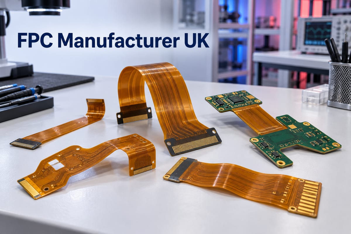
FPC manufacturer UK
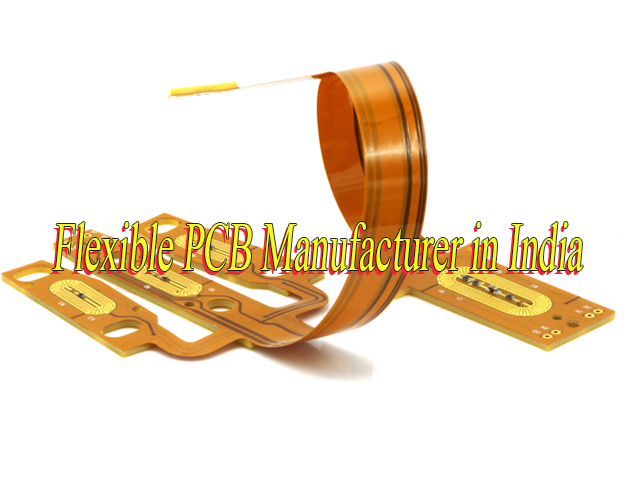
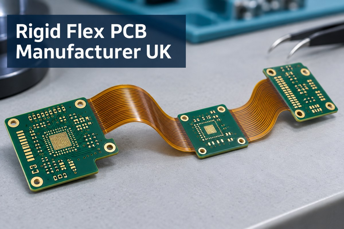
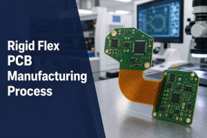
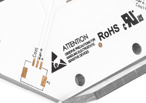
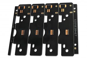
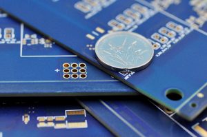
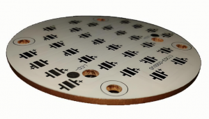
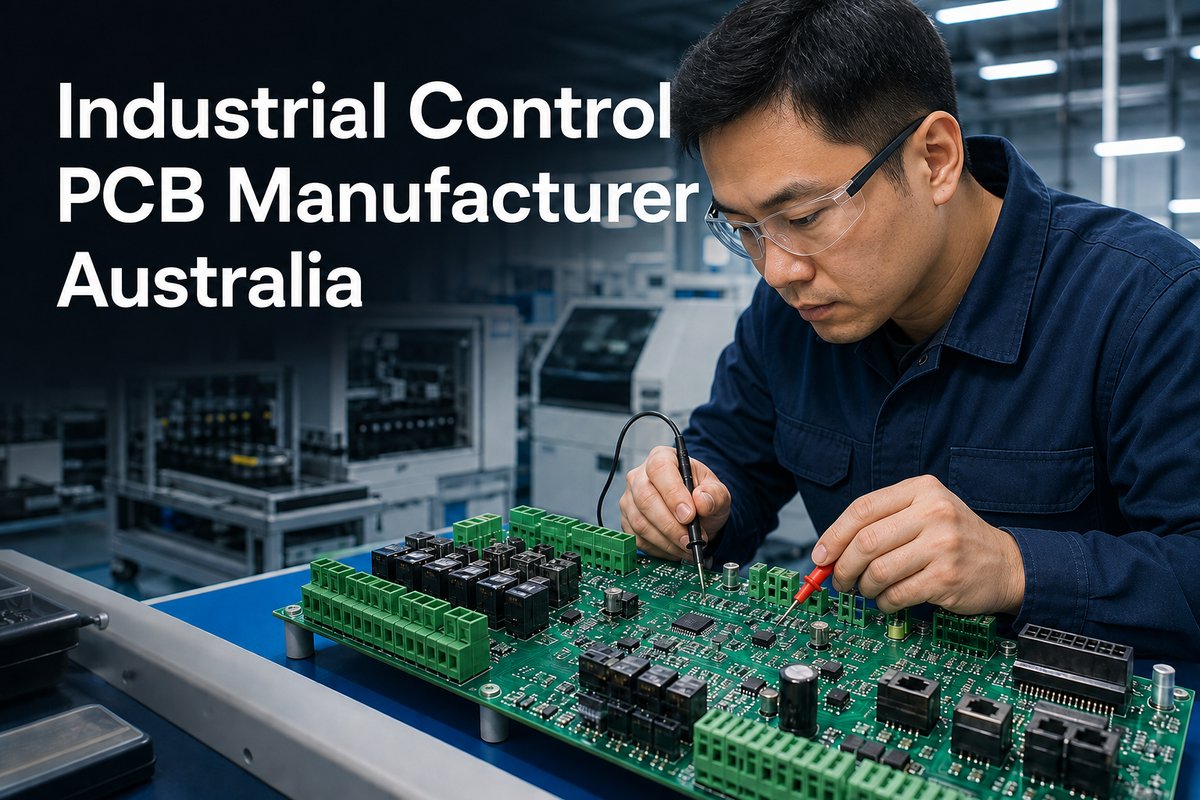
Flexible and rigid-flex PCB examples for UK manufacturing projects.

Which FPC Manufacturers Serve UK Projects?

The five companies below have identifiable UK manufacturing operations and publicly describe flexible or rigid-flex PCB capability. They are not ranked because their strongest applications are different.

Manufacturer UK operation Best suited to
GSPK Circuits North Yorkshire General flex, rigid-flex, and specialist PCB projects
Exception PCB Tewkesbury Complex multilayer, HDI, and advanced rigid-flex builds
Merlin Flex Hartlepool Dedicated flex manufacturing and added-value assembly
Amphenol Trackwise Stonehouse Long-length FPCs for aerospace, EV, medical, and industrial systems
Cambridge Circuit Company Cambridge In-house prototypes and fast-turn flex or flex-rigid boards

GSPK Circuits is a broad UK PCB manufacturer rather than a flex-only company. Its North Yorkshire facility produces flex and rigid-flex boards alongside HDI, RF, IMS, and other specialist constructions. GSPK is relevant when a project needs conventional or complex flexible circuitry from a manufacturer with a published process table and UK production.

Exception PCB manufactures flex and rigid-flex PCBs at its Tewkesbury facility. Its published capability extends to high-layer-count rigid-flex, fine features, laser microvias, and filled vias. It is a stronger candidate when the flex construction is part of a dense multilayer or HDI design rather than a simple flexible interconnect.

Merlin Flex is the dedicated flexible-circuit business within Merlin PCB Group. It manufactures flexible and flex-rigid PCBs in Hartlepool and also provides component assembly. Its specialist focus makes it relevant to customers who want a UK source centred on flex technology rather than a general PCB supplier that also offers flex.

Amphenol Trackwise occupies a distinct position. Its continuous roll-to-roll process produces multilayer flexible circuits that can extend far beyond conventional panel lengths. It is particularly relevant when an FPC replaces a large wiring harness in aerospace, electric-vehicle battery systems, medical equipment, or industrial machinery.

Cambridge Circuit Company offers in-house UK production of multilayer, flex, flex-rigid, plated-through-hole, and single-sided boards. The company emphasises prototype and fast-turn manufacturing, making it a practical option for development teams that prioritise short feedback loops and local production.
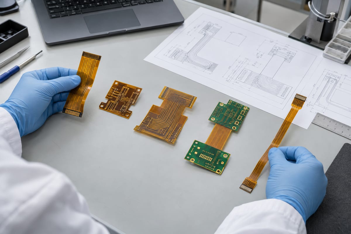
FPC manufacturer UK
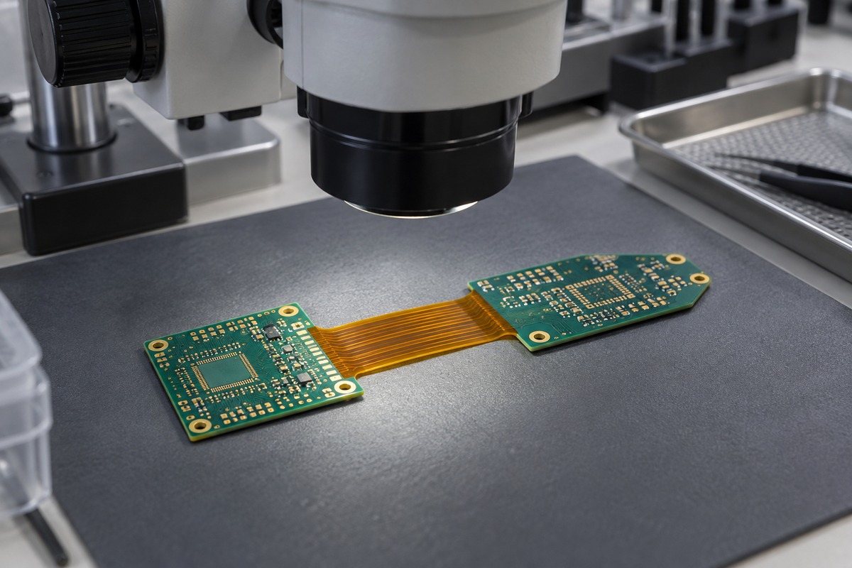
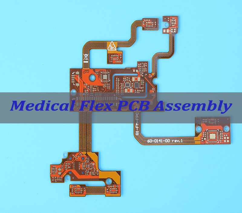
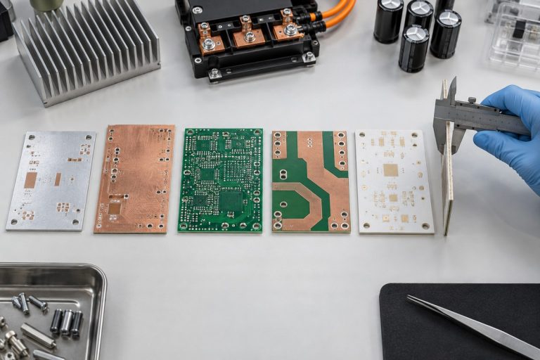
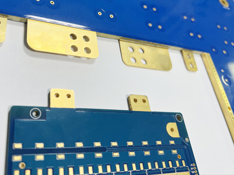
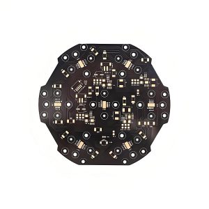
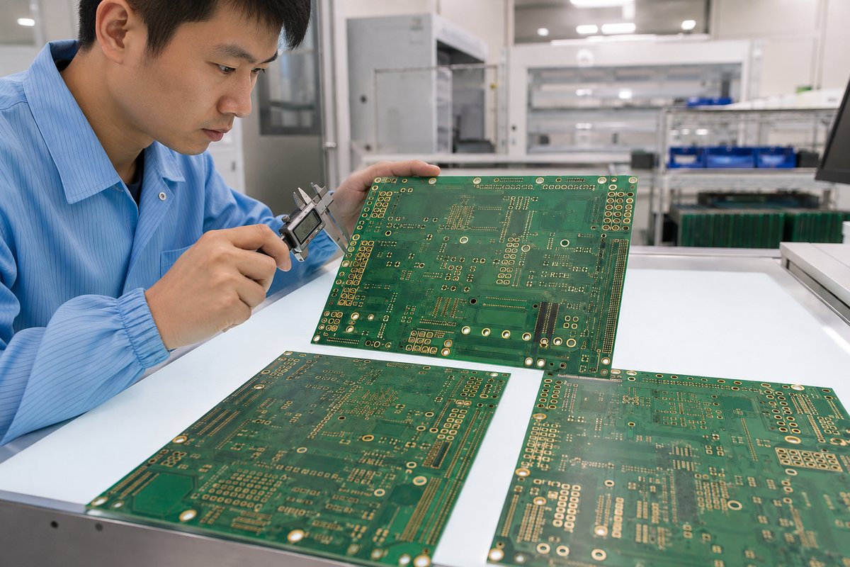
Comparing different flexible and rigid-flex constructions before selecting a manufacturing source.

How Do UK FPC Suppliers Differ by Application?

The best supplier depends on where the FPC will operate and what the finished product demands from it. UK manufacturers position their capabilities around different application markets.

Supplier strengths by application:

Application Relevant UK suppliers Best match
Aerospace and defence Trackwise, Exception PCB, Graphic PLC Long harness replacement or complex rigid-flex avionics
Automotive and EV Trackwise Battery-pack and cell-control interconnects
Medical equipment Trackwise, Graphic PLC Miniature interconnects and high-reliability flex-rigid
Industrial and scientific GSPK, Trackwise Conventional flex or extended power and signal routing
Consumer and wearable Merlin Flex, Cambridge Circuit General flex production and fast prototypes

Trackwise is most distinctive when circuit length or harness replacement drives the design. Exception PCB and Graphic PLC better match dense, high-reliability rigid-flex assemblies. GSPK covers a broader range of conventional and specialist flex builds, while Merlin Flex and Cambridge Circuit Company provide more general flex manufacturing or prototype routes. The last two matches are based on published manufacturing scope rather than a stated specialisation in consumer or wearable products.

Application is the first filter, not the final decision. After identifying suppliers active in the relevant market, compare the actual circuit construction with their published process capabilities.

Which Flex and Rigid-Flex PCBs Can UK Suppliers Produce?

UK manufacturers cover more than one type of flexible circuit. The construction should be matched to the product rather than selected from the name alone.

  • Single-sided FPCs: Suit simple connections, sensors, membrane-style interfaces, and low-density routing.
  • Double-sided FPCs: Provide more routing space and plated interconnection while remaining thinner and simpler than most multilayer constructions.
  • Multilayer FPCs: Support higher connection density, shielding, controlled routing, or a larger number of conductors in limited space.
  • Rigid-flex PCBs: Integrate rigid component areas and flexible interconnects into a single manufactured structure. They can remove separate cables and connectors, but the transition between rigid and flexible areas adds manufacturing complexity. Exception PCB, GSPK, Merlin Flex, and Cambridge Circuit Company all publicly present rigid-flex or flex-rigid capability.
  • Dynamic-flex circuits: Are designed for repeated movement rather than a single installation bend. They require greater attention to copper type, grain direction, bend radius, layer balance, conductor routing, and the position of coverlay or stiffener transitions. A supplier that can manufacture an FPC is not automatically the right source for a circuit expected to complete thousands or millions of bending cycles.
  • Long-length FPCs: Form a more specialised category. Trackwise uses a continuous manufacturing process for circuits that exceed standard panel dimensions. This construction is relevant when a product designer wants to replace a long cable harness with a thin, repeatable printed interconnect.

What Manufacturing Capabilities Do UK FPC Suppliers Offer?

GSPK publishes standard and advanced flex and rigid-flex manufacturing values. The figures below show what one established UK manufacturer states it can support; they should not be treated as universal limits for every UK supplier.

Capability Standard Advanced
Flex layers 2 8
Rigid layers 10 14
Overall thickness 0.20–3.20 mm 0.06–5.00 mm
Maximum board size 266.7 × 430 mm 350 × 500 mm
Inner track/gap, 17 µm copper 90 µm 50 µm
Outer track/gap, 17 µm base copper 100 µm 75 µm
Copper options 0.5 oz and 1 oz Up to 2 oz
Stiffener options Coverlay, FR-4, prepreg Aluminium also available

GSPK also lists HASL, lead-free HASL for single-sided FPCs, ENIG, and OSP for constructions without stiffeners. Larger board sizes and higher flex-layer counts may be available after review.

Three practical conclusions can be drawn from this table. First, UK manufacturing is not limited to simple one- or two-layer flexible circuits; GSPK publishes an advanced flex capability of eight layers and rigid sections up to fourteen layers. Second, fine-line capability changes with copper thickness and whether the conductor is on an inner or external layer, so a single “minimum track” number can be misleading. Third, layer count, thickness, board size, copper, finish, and stiffener requirements must be evaluated as one construction. A design cannot assume that every advanced limit can be combined simultaneously.
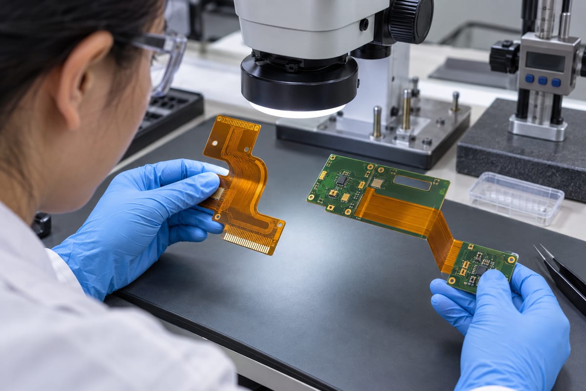
FPC manufacturer UK
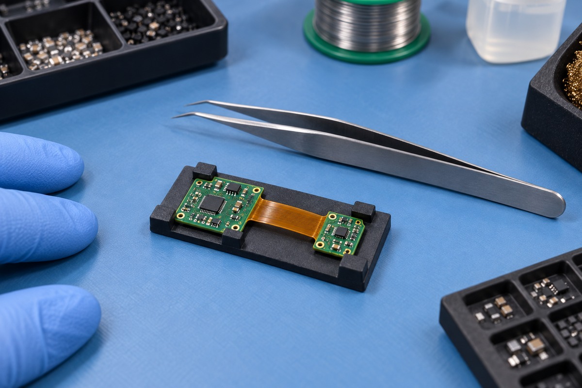
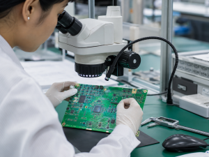
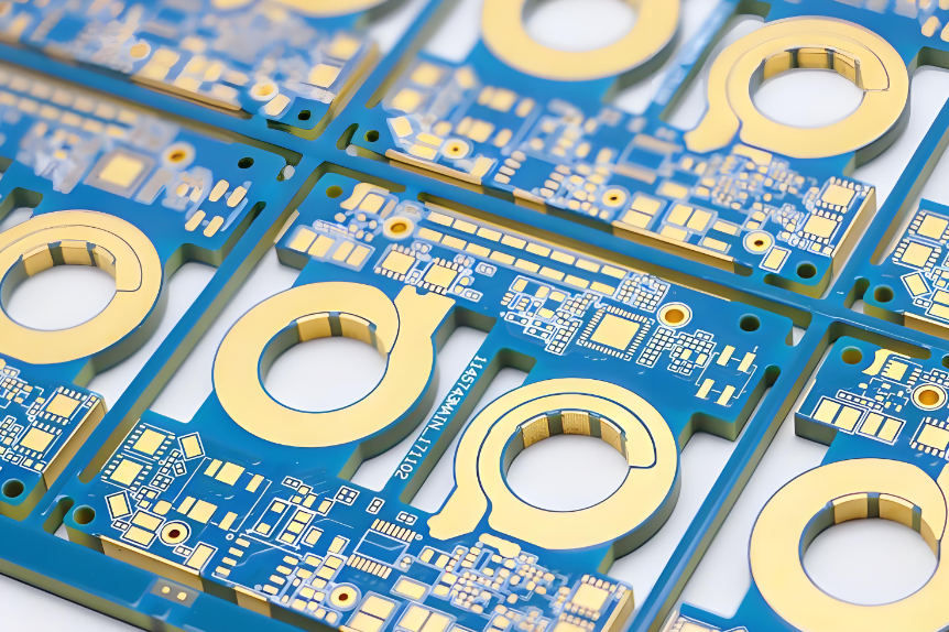
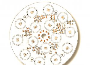
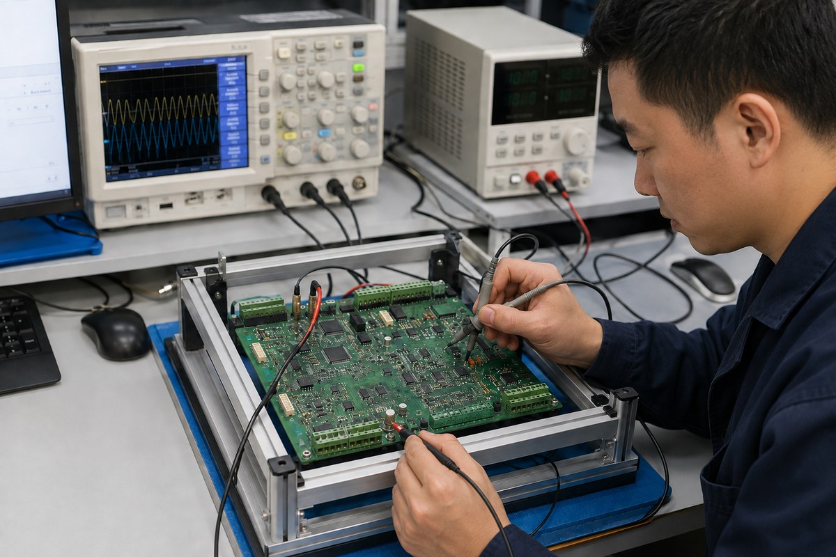
Inspecting flexible circuitry, coverlay features, connector areas, and rigid-flex transitions.

Which UK FPC Suppliers Support Aerospace and High-Reliability Applications?

For aerospace and high-reliability work, supplier fit becomes clearer when companies are compared by the manufacturing capability they publicly associate with demanding applications. The five examples below offer different strengths; they should not be treated as interchangeable.

UK manufacturer Relevant strength Projects it may suit
Amphenol Trackwise Roll-to-roll long FPC Aircraft harness replacement
Exception PCB 24-layer rigid-flex and HDI Dense avionics and defence boards
Graphic PLC Flex-rigid and advanced vias Avionics, space, and medical
GSPK Circuits UK specialist flex production Defence and controlled UK supply
PW Circuits Flex-rigid and Class 3 High-reliability, mid-volume builds

Amphenol Trackwise is the most distinctive choice when circuit length is the central problem. Its continuous roll-to-roll process supports working panels up to 100 metres long and 630 mm wide, with up to eight copper layers for prototypes and four for production, subject to construction. Trackwise states that it has manufactured a flexible multilayer circuit longer than 72 metres. This capability is relevant when a printed circuit replaces wiring across an aircraft wing, vehicle battery system, or other large structure; it adds little value to an ordinary short FPC.

Exception PCB is more relevant when high reliability is combined with dense rigid-flex construction. Its published capability includes up to 24 rigid-flex layers, up to 12 flex layers, track and gap down to 60 µm on its advanced process, laser microvias down to 75 µm, and copper or resin via filling. These features make it a stronger candidate for compact assemblies in which the rigid section carries HDI components while the flex section replaces separate interconnects.

Graphic PLC positions its UK manufacturing around high-technology PCBs for avionics, space, security, medical, and other high-reliability sectors. Its stated strengths include flex-rigid construction, HDI, blind and buried vias, filled and stacked vias, and sequential build-up. It may therefore be relevant when the project needs both flex-rigid integration and advanced via structures.

GSPK Circuits offers a broader specialist-PCB route from its North Yorkshire facility. Its published material identifies defence as a sector that can benefit from controlling processes such as ENEPIG internally rather than sending boards to an external subcontractor. This may matter when the customer values UK production and a shorter, more visible manufacturing chain alongside flex or rigid-flex capability.

PW Circuits publicly lists single- and double-sided flex, multilayer flex-rigid, specialist material experience, and IPC 6013 Class 3 among its capabilities and approvals. It may suit customers that need UK prototype-to-mid-volume production and requirements associated with more demanding flexible-circuit acceptance.

The useful distinction is not that all five companies serve “high reliability.” Trackwise solves unusual circuit-length problems; Exception PCB and Graphic address complex constructions; GSPK offers broad specialist production with UK process control; and PW Circuits combines flex capability with demanding-board approvals. The application and released construction determine which strength is relevant.
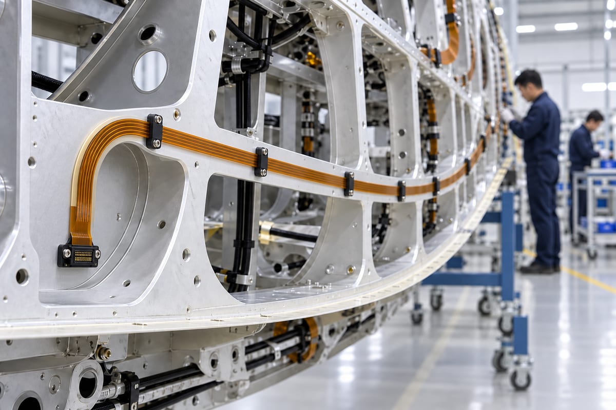
FPC manufacturer UK
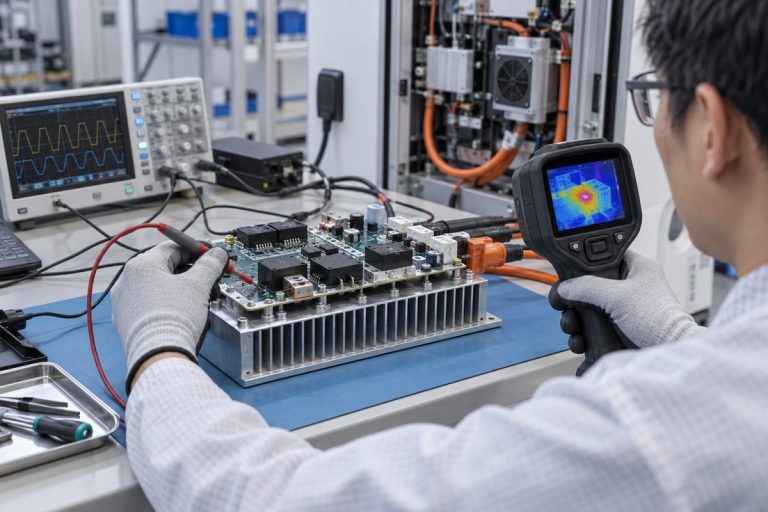
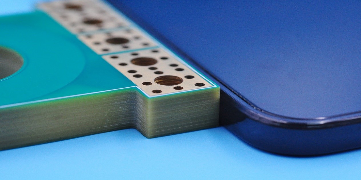
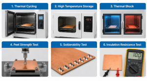
An illustrative long flexible circuit routed through a large high-reliability equipment structure.

UK Manufacturing or Offshore Production: Which Model Fits?

The right model depends on what the project needs at its current stage.

UK manufacturing is a stronger fit when:

  • local production or supply-chain visibility is required;
  • early revisions need rapid engineering feedback;
  • an unusual construction benefits from close technical discussion;
  • low-volume or urgent prototypes are the immediate priority.

Offshore production is a stronger fit when:

  • the design is stable and volumes are expected to grow;
  • production cost is important;
  • multilayer flex, rigid-flex, sourcing, and PCBA need one supply route;
  • international logistics can be planned into the schedule.

A hybrid route can fit when:

  • a UK factory supports development or urgent prototypes; and
  • a qualified offshore factory handles repeat production.

The choice is not “UK quality” versus “offshore cost.” Whichever model is used, materials, stack-up, copper type, coverlay openings, stiffeners, bend regions, finish, and testing must remain controlled. Otherwise, the prototype and production board may look similar while behaving differently.

How Can EBest Circuit Support UK FPC Projects?

EBest Circuit (Best Technology) is an offshore option for UK customers that need flexible or rigid-flex PCB production beyond a local prototype order. Its role is to give the customer one technical route from a released design to repeat manufacturing, while keeping the construction agreed during quotation visible throughout the project.

Support for UK projects centres on four practical outcomes:

  • Direct technical communication: Questions about the stack-up, polyimide, copper, coverlay, stiffeners, bend areas, and finish are resolved with the manufacturing team before production. This reduces the risk of commercial messages being passed between the customer, a broker, and an unidentified factory.
  • A controlled move from prototype to production: The agreed materials, layer structure, flex thickness, openings, and test requirements can remain part of the same manufacturing definition as quantities increase. The customer does not need to restart the technical discussion simply because the project moves beyond its first build.
  • Offshore production with a defined scope: UK customers can use EBest Circuit when local production does not provide the required commercial fit, production capacity, or flex and rigid-flex process range. The value comes from matching the released construction to an established process, not from choosing an offshore quotation on price alone.
  • Optional fabrication-to-assembly continuity: When the project includes connectors or mounted components, sourcing and PCBA can follow the same technical handoff. When only bare FPCs are required, the project can remain fabrication-only without an unnecessary assembly package.

The manufacturing capabilities discussed earlier in this article provide the technical basis for this support. EBest Circuit confirms the usable combination for each design rather than assuming that separate maximum values for layers, copper, thickness, and fine features can all be applied at once.

Send your Gerber or ODB++ data, drill files, stack-up, mechanical drawing, target quantity, and bending conditions to sales@bestpcbs.com. EBest Circuit can then confirm whether the design fits its manufacturing scope and whether bare-board production or a combined fabrication-and-assembly route is more appropriate.

FAQs About FPC Manufacturer UK

Are all companies appearing as UK FPC manufacturers producing boards in the UK?

No. Search results can include UK factories, local sales offices, PCB brokers, assembly companies, and overseas manufacturers serving UK customers. Verify the stated production location and the company responsible for manufacturing control rather than relying on the page title alone.

Which UK manufacturer is suitable for a complex rigid-flex PCB?

Exception PCB publicly presents high-layer-count rigid-flex, HDI, microvia, and via-filling capabilities, making it a relevant candidate for complex builds. GSPK and Merlin Flex also publish substantial flex and rigid-flex capabilities. The final choice should be based on the complete stack-up and feature combination rather than layer count alone.

Which UK manufacturer specialises in long flexible circuits?

Amphenol Trackwise specialises in long-length multilayer flexible circuits manufactured with a continuous roll-to-roll process. Its technology is most relevant when the FPC replaces an extended wiring harness or must span a structure much larger than a conventional PCB panel.

Can UK FPC manufacturers also assemble components?

Some can. Merlin Flex publicly includes added-value component assembly, while other UK suppliers may provide assembly internally or through partners. Confirm whether the same organisation controls fabrication and assembly, especially when connectors, stiffeners, and component areas interact mechanically.

When should a UK customer consider an offshore FPC manufacturer?

An offshore manufacturer may be appropriate when the design is sufficiently defined, production volume is expected to grow, pricing must remain competitive, or fabrication and PCBA need to be coordinated. The offshore source should still demonstrate that its materials and process limits fit the released construction.

If you are comparing a UK factory with an experienced offshore FPC manufacturer UK customers can work with directly, EBest Circuit can evaluate your design against practical fabrication and assembly capabilities. Contact sales@bestpcbs.com for a project-specific review.
You may also like

Buried Copper Coin PCB Manufacturer for Thermal Management

September 10th, 2026

A buried copper coin PCB manufacturer helps engineers create a short, solid-metal heat path through a multilayer circuit board. Instead of forcing concentrated heat through FR-4 and a field of small thermal vias, the design places a machined copper insert directly below or near the hot component. The result is localized thermal management without converting the entire assembly to a metal-core construction.

Buried copper coin technology is especially useful when a compact product combines high heat density with multilayer routing, controlled impedance, HDI features, or a backside heatsink interface. EBest Circuit (Best Technology) manufactures custom PCB and PCBA projects and can review whether a buried, embedded, or press-fit copper structure matches the intended board construction. Contact sales@bestpcbs.com to discuss your layer stack, hot component, copper coin geometry, quantity, and assembly requirements.

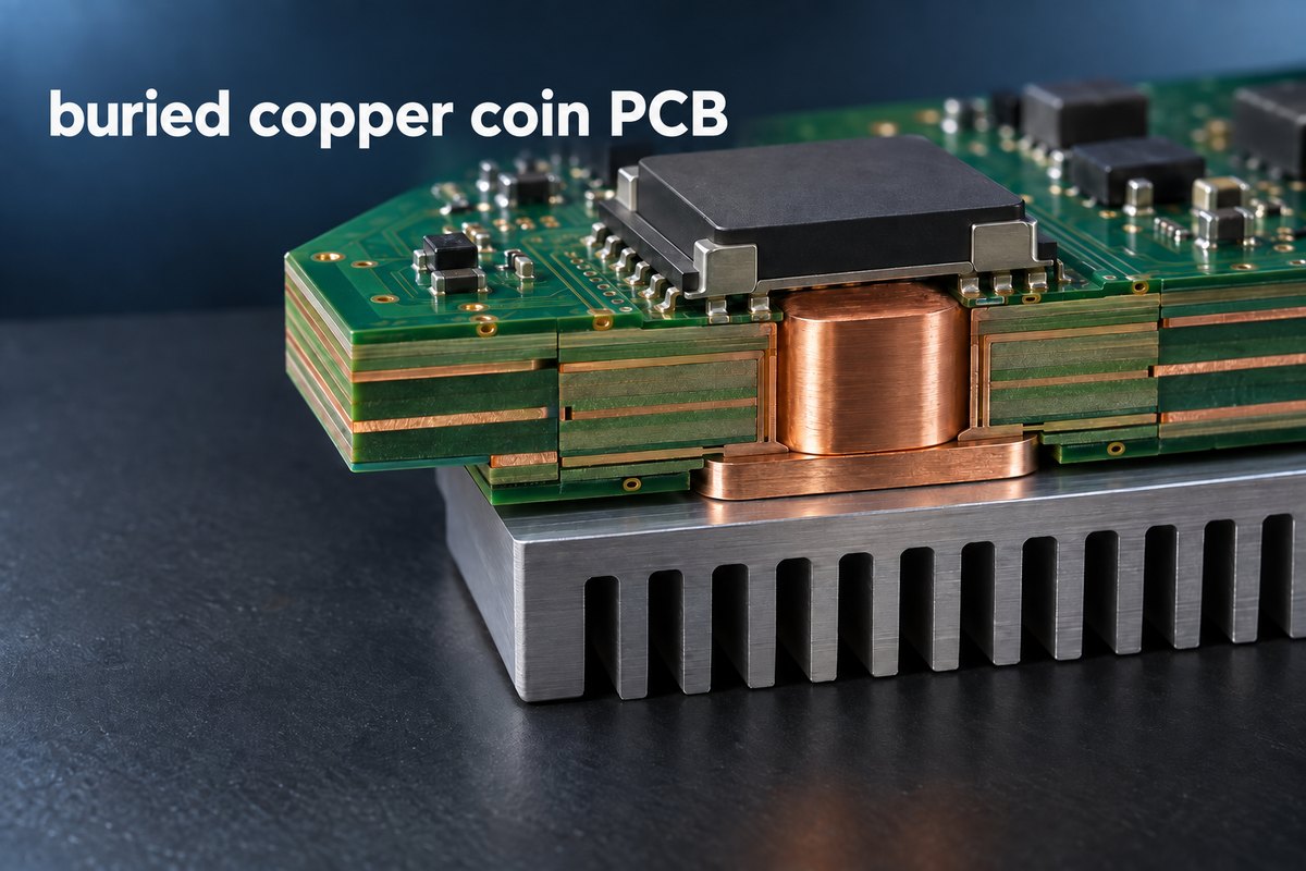
buried copper coin PCB
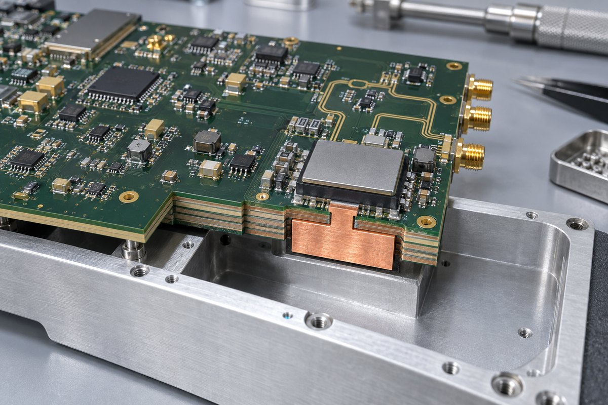
A multilayer buried copper coin PCB creates a direct solid-copper path from a heat-generating component to a backside heatsink.

What Is a Buried Copper Coin PCB?

A buried copper coin PCB contains a solid copper insert inside the PCB stackup, normally below a component or thermal pad that produces concentrated heat. Three details define the structure:

  • Position: The coin may sit completely inside the multilayer build or extend toward one or both outer surfaces.
  • Layer connection: It may connect an outer layer to an internal copper plane, join selected internal layers, or remain electrically isolated and serve only as a thermal path.
  • Shape: “Coin” does not mean round. Common forms include rectangular, square, T-shaped, stepped, and custom-machined inserts.

The geometry follows the heat-source area, available routing space, intended layer connection, and mechanical interface on the other side of the PCB.

Manufacturers do not always use “buried,” “embedded,” and “press-fit” in exactly the same way. A cross-sectional drawing is therefore more useful than the name alone because it shows whether the coin is fully enclosed, exposed at one surface, exposed at both surfaces, or inserted into a finished cavity.

buried copper coin PCB
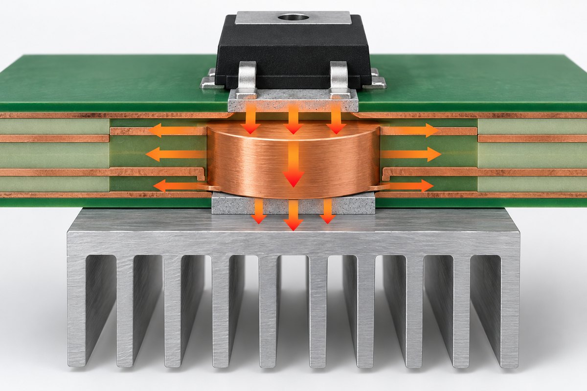
A copper coin conducts heat vertically toward the heatsink and laterally into connected copper planes.

How the Buried Copper Coin Transfers Heat

Heat follows every available path away from a component. In an ordinary multilayer PCB, heat may travel laterally through the surface copper, downward through thermal vias, and then into inner planes, a backside copper area, or a heatsink. This approach works well for many components, but the path contains interfaces and materials with much lower thermal conductivity than solid copper.

A copper coin replaces part of that path with a continuous copper body. When the component pad, copper coin, thermal interface material, and heatsink are aligned, heat can move through a much larger solid-metal cross-section. The coin can also spread heat into connected copper planes before it reaches the opposite side of the board.

The improvement does not come from copper alone. It comes from the complete path:

  • The component must transfer heat efficiently into the top surface or connected copper layer.
  • The coin must have enough contact area at the heat source.
  • Intended copper layers must connect to the coin without narrow thermal bottlenecks.
  • The opposite side must transfer heat into a chassis, cold plate, heatsink, or other cooling structure.
  • Thermal interface material and mounting pressure must support the intended contact.

For this reason, a large coin does not automatically guarantee a low component temperature. Junction-to-case resistance, solder coverage, contact flatness, interface material, airflow, and heatsink capacity remain part of the thermal system. The PCB coin solves the board-level section of the heat path; it does not replace complete thermal analysis and product testing.

buried copper coin PCB
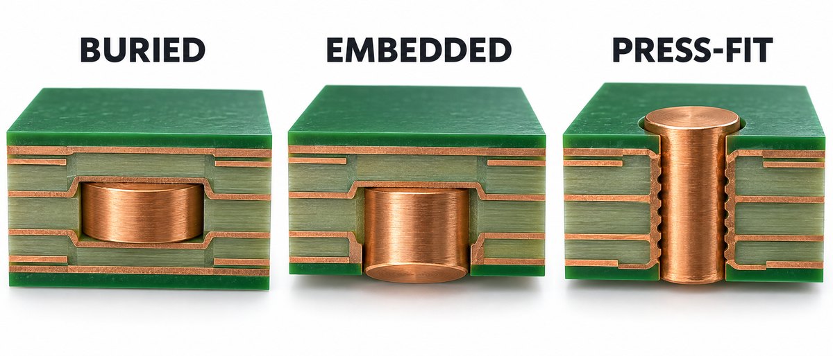
Buried, embedded, and press-fit copper coin structures use different insertion and exposure methods.

Buried, Embedded, and Press-Fit Copper Coin Structures

Copper coin constructions are commonly grouped by when the insert is added and how it sits inside the board.

Buried copper coin: The insert is incorporated within the multilayer build and does not necessarily pass through the complete board thickness. It can connect selected layers while leaving routing space above or below it. This structure is useful when the thermal path must begin at an internal or subsurface layer, or when an outer layer needs to remain available for routing or component features.

Embedded copper coin: The coin is built into the PCB during multilayer fabrication and may be exposed at one or both surfaces. It can form a mounting or thermal contact surface while remaining integrated with the surrounding laminate. Some suppliers also use “embedded” as the general category that includes buried coins.

Press-fit copper coin: A machined copper part is inserted into a prepared PCB opening with controlled interference. This construction can create a direct path through the board without embedding the coin during lamination. Hole geometry, coin tolerance, insertion force, retention, and surface height all influence the finished result.

Conductive adhesive can also be used for certain copper inserts, depending on the structure and factory capability. Each method changes the mechanical interface, achievable layer connections, thermal contact, manufacturing sequence, and cost. The construction drawing should identify the actual cross-section rather than relying only on one of these category names.

Copper Coin Shapes and Layer Connections

The coin shape determines how heat moves between the component, PCB layers, and external cooling surface.

  • Straight rectangular coin: Creates a simple vertical path when the hot pad and backside cooling area have similar dimensions. The upper and lower contact areas remain aligned.
  • T-shaped coin: Connects two differently sized interfaces. A narrow upper section can fit beneath a small component pad, while a wider lower section spreads heat toward a larger heatsink or housing contact area. The orientation can also be reversed.
  • Stepped coin: Stops at a selected depth or creates different contact areas at different layers. It can connect two internal planes without reaching the component side, or connect a top pad to an inner power plane while leaving lower layers available for routing.
  • Connected or isolated coin: Selected layers may connect directly, through plating, or through defined copper features around the insert. Other layers use clearance to remain electrically isolated.
  • Thermal-only or electrical-and-thermal coin: The insert can transfer heat only, or it can also carry current or connect to ground. An electrical function must be reflected in the schematic, netlist, clearance, and test plan.

A wider coin generally provides more contact area and heat spreading but occupies more routing space and may interrupt internal planes. A smaller coin preserves board area but reduces the available heat-flow cross-section. The final shape must balance the thermal interface with routing, stackup, component placement, and mechanical packaging.

Buried Copper Coin PCB Manufacturing Process

The exact sequence depends on whether the coin is buried during lamination, embedded with an exposed surface, bonded, or press-fitted after the PCB structure is formed. A typical buried or embedded process follows five main stages:

  1. Machine the copper coin. The insert is produced to the specified shape and thickness. Its surface may also be prepared for resin bonding, plating, or a defined copper connection.
  2. Create the matching PCB cavity. The relevant core, prepreg, or subassembly is machined so the coin can occupy its intended position in the stackup.
  3. Position and laminate the structure. The coin is placed during layup, and the multilayer panel is pressed under a controlled cycle. Prepreg resin flows around the insert and fills the intended interface.
  4. Establish the finished surface. After lamination, planarization or controlled machining may be used to achieve the specified exposed area and surface height.
  5. Complete PCB fabrication. The panel continues through the applicable drilling, plating, imaging, etching, solder-mask, surface-finish, routing, and inspection operations.

The copper insert and laminate respond differently to heat and pressure, so cavity geometry, resin volume, stack symmetry, and coin restraint influence the laminated result. If the coin forms a solderable pad, its finished surface must match the assembly design. If it contacts a heatsink or chassis, its usable contact area and height must suit that interface.

For a press-fit construction, the PCB opening and copper part are manufactured separately and then joined by controlled insertion. This avoids embedding the coin during lamination but makes opening dimensions, insertion force, retention, and surface height important. In either approach, the product is a combined PCB, copper-part, and assembly structure—not a standard PCB with an unrelated metal piece added later.

Where Buried Copper Coin PCBs Are Used

Buried copper coin PCBs are used where a small number of components create concentrated heat and the product still requires the routing density or layer count of a conventional multilayer board.

RF and telecommunications equipment: Power amplifiers, radio units, base-station electronics, and other RF assemblies may place a copper coin beneath a high-power device while preserving controlled-impedance routing around it.

Power conversion: DC-DC converters, power supplies, inverters, charging equipment, and power-distribution modules can use copper coins beneath switching devices, power packages, or localized high-current areas.

Industrial and motor-control electronics: Servo drives, motor controllers, robotics controllers, and compact industrial modules may need a direct path from a hot device to a chassis or cold plate.

High-output LED systems: Dense LED modules and illumination controllers can use a copper insert where one device or cluster produces a localized hot spot that exceeds the capability of ordinary vias and surface copper.

Automotive and transportation electronics: Compact power and communication modules may combine high heat density, vibration, restricted airflow, and a housing-based cooling path. The complete construction must still be validated for the applicable operating environment.

Aerospace and defense electronics: Space-constrained RF and power assemblies may use localized solid-copper heat paths when weight, routing density, mechanical design, and reliability requirements justify the additional PCB complexity.

Copper coins are less attractive when heat is spread uniformly across the entire board, when ordinary thermal vias already meet the temperature target, or when the product lacks a useful destination for the extracted heat. In those situations, thicker copper, a metal-core PCB, a larger heatsink, improved airflow, or a different component layout may be more economical.

Buried Copper Coin PCB vs. Thermal Vias and Metal-Core PCBs

Thermal vias, copper coins, and metal-core PCBs solve different thermal layouts.

Thermal vias are easy to include beneath many exposed-pad components and fit normal multilayer manufacturing. They transfer heat through multiple plated barrels into internal or backside copper. They are generally the first option when the heat load and available pad area are compatible with a via array.

A buried copper coin concentrates a larger solid-copper cross-section at one hot location. It is useful when a via field would occupy too much pad area, provide insufficient through-thickness conduction, or interfere with the required package and stackup. It also allows the rest of the PCB to remain a conventional multilayer or HDI construction.

A metal-core PCB uses an aluminum or copper base to spread heat across a much larger portion of the board. It is well suited to many LED, power, and high-temperature assemblies, but the dielectric between the circuit copper and metal base remains part of the thermal path. Multilayer routing and plated-through interconnection can also be more constrained than on a conventional FR-4 multilayer board.

The choice is therefore not simply “which material conducts heat best?” Thermal vias favor simplicity and cost; copper coins favor intense localized heat transfer in a complex multilayer board; metal-core PCBs favor broader heat spreading across the assembly. Some products combine these methods with heavy copper, thermal interface materials, heatsinks, cold plates, or enclosure cooling.

buried copper coin PCB
An eight-layer RF control board can use a T-shaped copper coin beneath a power amplifier to reach the aluminum housing.

A Practical Buried Copper Coin PCB Example

Consider an eight-layer RF control board with a power amplifier near one edge.

  • Board requirements: The amplifier connects to controlled-impedance RF traces on the top layer, while digital control and power routing occupy several inner layers. A machined aluminum housing below the PCB is the main cooling surface.
  • Why not a metal-core PCB: A full metal base would complicate the multilayer routing and interconnection required by the RF and control circuits.
  • Why not thermal vias alone: A large via field would consume much of the exposed-pad area and still rely on multiple plated barrels for vertical heat transfer.
  • Selected structure: One T-shaped copper coin sits beneath the amplifier. Its narrow upper section matches the component’s thermal land, while its wider lower section increases contact area toward the housing.
  • Layer and housing connection: Selected ground layers connect to the coin for lateral heat spreading, while signal layers clear the copper body. A thin thermal interface material connects the finished coin surface to the housing after assembly.

The value of this structure is not simply “more copper.” The T-shape connects a small heat source to a larger cooling surface without sacrificing the multilayer routing required by the circuit.

This example is illustrative rather than universal. Actual coin size, surface height, layer connections, finish, interface material, and cooling performance must follow the component power, package data, thermal simulation, housing design, and prototype results.

Why Choose EBest Circuit for Buried Copper Coin PCB Manufacturing?

A buried copper coin PCB requires the copper insert, PCB cavity, multilayer stackup, layer connections, surface height, and assembly interface to work together. EBest Circuit (Best Technology) supports these projects with coordinated engineering, PCB fabrication, component sourcing, and PCBA services.

  • One coordinator backed by three engineers: Each project is supported by one business coordinator and three engineers, helping customer questions move quickly between PCB, PCBA, component, and process teams.
  • DFM review by experienced engineers: Engineers with up to 20 years of PCB, PCBA, and product-development experience can review the copper coin structure, cavity, stackup, connected and isolated layers, surface finish, and assembly interface. Customers can receive a DFM review and applicable process recommendations before production.
  • Integrated PCB and PCBA services: EBest Circuit combines PCB manufacturing, component sourcing, PCBA assembly, and testing, reducing the need to coordinate the copper coin PCB and subsequent assembly with separate suppliers.
  • Prototype and low-volume support: Prototype and low-volume production can support engineering verification before the design moves to a larger production quantity.
  • Factory and quality-system support: EBest Circuit operates PCB and PCBA manufacturing facilities under quality systems including ISO 9001, ISO 13485, IATF 16949, and AS9100D.

With 20 years of PCBA experience, EBest Circuit has served more than 10,000 engineers and over 1,800 customers. If you are developing an RF amplifier board, power converter, motor controller, LED system, or another high-heat-density product, send your PCB data, stackup, and copper coin drawing to sales@bestpcbs.com. The team will review the manufacturing requirements and prepare a project-specific quotation.

FAQs About Buried Copper Coin PCB

Is a buried copper coin always completely enclosed inside the PCB?

Not necessarily. Terminology varies among manufacturers. Some buried coins are fully enclosed, while others stop at or become exposed on a selected surface. The cross-section and stackup should define the actual structure.

Can a copper coin carry electrical current as well as heat?

Yes, when it is intentionally connected to a circuit net or ground structure. In that case, current capacity, layer connections, clearances, netlist data, and electrical testing must be considered together with thermal performance.

Is a copper coin better than a thermal-via array?

It can provide a more direct solid-copper path for a concentrated heat source, but it is more complex and costly to manufacture. Thermal vias remain suitable for many components. The correct choice depends on heat density, package geometry, routing, stackup, cooling interface, and cost target.

Can buried copper coins be used in HDI or rigid-flex PCBs?

They can be combined with some high-layer-count, HDI, and rigid-flex constructions, but the feasible structure depends on the individual factory, stackup, cavity, via arrangement, flex location, and lamination sequence. The complete build should be reviewed before release.

What information is most important for a copper coin quotation?

The most useful starting information is the PCB data, stackup, coin cross-section and dimensions, intended layer connections, component and heatsink interfaces, material and finish, quantity, and target application. These details allow the manufacturer to identify the appropriate production route and confirm project-specific capability.

Planning a buried copper coin PCB? Send your PCB files, stackup, copper coin drawing, intended layer connections, quantity, and assembly requirements to sales@bestpcbs.com. EBest Circuit will review the manufacturing requirements and prepare a project-specific quotation.

You may also like

Rigid Flex PCB Manufacturer UK: Top 10 Suppliers to Compare

September 9th, 2026

Looking for a rigid-flex PCB manufacturer for your UK project? The right partner should match your board’s complexity, budget and delivery needs. This guide compares ten UK-based manufacturers and suppliers, helping you assess manufacturing capabilities, lead times and assembly options before choosing where to place your order.

EBest Circuit (Best Technology) combines experience manufacturing a 14-layer rigid-flex PCB for a UK medical-product customer with PCB fabrication, component sourcing and assembly services. For buyers with complex boards, that combination offers relevant manufacturing experience and the option to coordinate bare boards and assembly through one supplier. Email sales@bestpcbs.com to discuss your project or arrange a visit to our factory in China and meet the team behind your boards.

rigid flex PCB manufacturer UK
Rigid-flex PCB construction

Rigid Flex PCB Manufacturer UK: 10 Suppliers Compared

The shortlist below covers ten UK-based businesses offering rigid-flex PCB manufacture or supply. It includes UK manufacturers and UK suppliers using partner factories; the service model is identified for each entry. The numbering is for comparison, not an independently audited ranking.

UK business Capability focus
1. Newbury Electronics Fabrication and assembly
2. GSPK Circuits Flex and rigid-flex
3. Graphic HDI and flex-rigid
4. Cambridge Circuit Prototypes to volume
5. PCB Runner Limited Rigid-flex supply
6. Merlin Flex Flex-rigid and assembly
7. Exception PCB Complex rigid-flex
8. Amphenol Trackwise Extended-length flex / rigid
9. Daleba Flex and rigid-flex supply
10. ICAPE-ALR Partner-factory sourcing

Newbury Electronics manufactures flexible and flexi-rigid boards and offers electronic assembly. It is relevant when comparing a UK fabrication route with assembly support.

GSPK Circuits publishes separate rigid-layer and flex-layer capabilities, alongside material and surface-finish options. Its technical information helps buyers compare the actual board construction.

Graphic is a UK manufacturer specialising in complex PCBs, including flex-rigid, HDI and advanced via structures. Its stated focus includes demanding, high-reliability applications.

Cambridge Circuit Company offers flex and flex-rigid boards and discloses an offshore partner for larger volumes. Confirm which production route applies when moving from prototypes to repeat orders.

PCB Runner Limited is an active UK-registered company offering flex and rigid-flex services. Its registration establishes the UK business entity; confirm the manufacturing site for your order separately.

Merlin Flex manufactures and assembles flexible and flex-rigid circuits from Hartlepool. It offers a specialist UK route for buyers considering both board fabrication and assembly.

Exception PCB manufactures flex and rigid-flex boards at its UK facility in Tewkesbury. Its published capability covers complex constructions, with engineering review of stackups and rigid-to-flex transitions.

Amphenol Trackwise manufactures at Stonehouse, Gloucestershire. Its Improved Harness Technology capability includes flex/rigid formats and is particularly relevant when comparing extended-length interconnect options. Confirm the suitability of its process for your board construction.

Daleba is based in Hertford and supplies flex and rigid-flex boards in different materials and finishes. Treat it as a UK supply option and confirm the assigned manufacturing location for your order.

ICAPE-ALR, operating as ALR Services Limited in England, sources PCBs through a manufacturing network. Its technical portfolio includes multilayer flex and flex-rigid boards. It is a UK supplier rather than a claim of UK in-house rigid-flex fabrication.

How Do You Choose a Rigid-Flex PCB Manufacturer for Your UK Project?

Start with the type of rigid-flex board you need. A supplier that can make a simple flexible interconnect is not automatically the right fit for a multilayer board with several rigid sections, controlled impedance and a constrained folded shape.

Your shortlist should reflect the construction and the intended use. In particular, distinguish a board that bends during installation from one that must move repeatedly in service. Those conditions influence the flexible section, material selection and validation approach. Newbury also distinguishes static and dynamic applications in its material guidance.

Compare suppliers on four practical dimensions:

  • Construction fit: Experience with the required rigid and flex layers, transitions, via structures and finished geometry.
  • Order fit: A production model that suits your prototype quantity, repeat batches and expected demand.
  • Quality fit: Inspection and test arrangements appropriate to the board’s application and agreed acceptance requirements.
  • Communication fit: Clear technical responses, revision handling and a realistic production schedule.

A useful technical response addresses your actual board. For example, it explains whether the requested stackup is manufacturable and identifies any proposed changes. A generic statement that a factory makes “up to” a certain number of layers does not establish that your particular construction is within its routine process.

rigid flex PCB manufacturer UK
Rigid-flex PCB inspection

UK vs Overseas Rigid-Flex PCB Manufacturers: Which Fits Your Project?

UK manufacturing can be a practical choice when site access, local engineering discussions or domestic production are important to your programme. A nearby factory may also simplify the movement of samples between the PCB supplier, assembler and engineering team.

Overseas manufacturing broadens the range of suppliers you can compare. It can suit projects with an established design and a planned ordering cycle, but its value depends on the complete supply arrangement. A lower board price does not by itself establish a lower delivered cost.

Factor UK manufacturing Overseas manufacturing
Communication Local meetings Remote reviews / time zones
Logistics Domestic transport International freight
Production Check batch capacity Check capacity and shipping
Origin Verify UK factory Verify assigned factory
Order changes Confirm production cut-off Confirm production and dispatch cut-offs

Some suppliers combine both routes. Cambridge Circuit Company, for example, discloses an offshore partner for larger-volume flex and flex-rigid orders. Ask whether prototype and production boards will use the same facility and process before treating them as one continuous supply route.

EBest is a China-based option for UK customers. Its location should be considered openly alongside the proposed technical solution, commercial terms and delivery plan.

What Affects Rigid-Flex PCB Manufacturing Costs for UK Orders?

Rigid-flex PCB pricing depends on the construction, manufacturing effort and number of usable boards produced from each panel. The UK delivery destination adds a logistics dimension, but it does not change the underlying complexity of the circuit.

Layer arrangement is an important starting point. Two boards with the same total layer count can require different processes if their flexible layers, rigid sections or via structures differ. Material availability and the amount of custom processing also affect the quotation.

Board shape matters because it influences panel utilisation. Long flexible tails, separated rigid sections and unusual outlines can leave material that cannot be used for another board. Order quantity then determines how setup and tooling costs are spread across the batch.

The main cost drivers are:

  • Rigid and flexible layer construction, materials and copper requirements.
  • Board dimensions, outline complexity and panel utilisation.
  • Via technology, feature sizes and additional processing.
  • Quantity, tooling and inspection or test scope.
  • Assembly, components and fixtures when populated boards are required.
  • Freight and any separately charged delivery or import handling.

Where the design allows it, discussing a supplier’s established stackups early may reduce custom processing. Any alternative must still satisfy your design requirements.

Compare quotations using the same revision, quantity and supply scope. Otherwise, a price difference may reflect different assumptions rather than a more competitive manufacturing offer.

How Long Does Rigid-Flex PCB Manufacturing and Delivery to the UK Take?

EBest’s rigid-flex lead-time guide lists 2 weeks for standard 4-layer production, with a fastest service of 1.5 weeks. Boards above 4 layers require a project-specific schedule.

Rigid-flex board Standard service Fastest service
4 layers 2 weeks 1.5 weeks
More than 4 layers Confirm per project Confirm per project

These figures cover the manufacturing service. Confirm UK shipping time separately, along with the start date and availability of the quoted service. The 14-layer medical board featured below needs its own schedule; the 4-layer timing does not apply.

For a realistic UK arrival date, allow for:

  • Engineering review: Resolve stackup questions and approve production data.
  • Board fabrication: Use the lead time confirmed for your construction.
  • Assembly, if required: Include component availability and assembly time.
  • UK delivery: Add transport and import handling to the dispatch date.

Share your required arrival date when requesting a quotation. This lets the team assess the manufacturing and shipping plan against the date you actually need the boards.

Can One Manufacturer Handle Both Rigid-Flex PCB Fabrication and Assembly?

Yes. EBest offers rigid-flex fabrication alongside component sourcing and PCB assembly. You can order bare boards for your UK assembler or discuss a populated-board supply through one supplier.

Choose the scope that suits your production setup:

  • Bare boards: Keep component sourcing and assembly with your existing team.
  • Turnkey assembly: Ask EBest to coordinate boards, component sourcing and assembly.
  • Partial turnkey or consigned assembly: Supply selected components or the full component kit, with responsibilities agreed in advance.

Why coordination matters for rigid-flex boards:

  • Board support: Flexible sections may need carriers during placement and soldering.
  • Moisture control: Agree storage and drying before reflow; polyimide absorbs moisture.
  • Test coverage: Bare-board electrical testing and assembled-board functional testing serve different purposes.

To discuss assembly, provide the BOM and placement data with your PCB files. Include any functional-test requirements so the quotation covers the finished-board scope you need.

rigid flex PCB manufacturer UK
Rigid-flex PCB assembly

Case Study: Rigid-Flex PCB Manufacturing for a UK Customer

EBest Circuit manufactured a 14-layer rigid-flex PCB for a UK customer’s medical product. The project combined defined board thickness and material requirements with controlled impedance.

The customer specified the following:

Item Project requirement
Application UK medical product
Board construction 14-layer rigid-flex PCB
Total thickness 1.4 mm ±10%
Material Tg 180°C
Surface finish ENIG, 1 µin gold
Mask / legend Green / white
Impedance 85 Ω ±10%

The 14-layer construction and 1.4 mm thickness requirement made the layer arrangement central to the manufacturing specification. The 85 Ω impedance target added an electrical requirement that had to be considered alongside that construction. These parameters describe the customer’s specified board; the impedance tolerance is a requirement, not a reported measurement.

This project provides a concrete example of EBest’s rigid-flex manufacturing work for a UK medical-product customer. It also illustrates why buyers should compare experience with a defined combination of layers, thickness, finish and impedance, rather than layer count alone.

Why Choose EBest Circuit for Your Rigid-Flex PCB Project?

EBest Circuit (Best Technology) is an option for UK buyers who want to source rigid-flex boards from a China-based manufacturer and discuss assembly within the same supply relationship.

Integrated rigid-flex construction. EBest’s published product offering covers rigid and flexible substrates laminated into one electrically interconnected board. Its examples include several multilayer arrangements, allowing the discussion to start with the structure your product needs.

Fabrication and assembly options. Buyers can discuss bare boards or a broader assembly requirement. EBest’s assembly offering includes component sourcing and multiple assembly service models, so the supply scope can be matched to how much work your own team or UK assembly partner will retain.

A project-specific discussion. Share the rigid-flex construction, order quantity and target delivery date so the proposed manufacturing route can be assessed against your requirements. If assembly is needed, include the BOM and placement data. The resulting offer should make the board scope, assembly scope and delivery assumptions clear.

To discuss your UK rigid-flex PCB project, contact sales@bestpcbs.com.

FAQs About Rigid Flex PCB Manufacturer UK

Is a supplier with a UK address necessarily manufacturing rigid-flex PCBs in the UK?

No. A UK address may be a sales or service location, and some suppliers use more than one manufacturing route. Confirm the facility proposed for your order, including any change between prototype and production.

Are rigid-flex PCB and flex-rigid PCB the same thing?

The terms commonly describe the same family of boards. However, terminology alone is insufficient: confirm the actual layer construction, because an integrated rigid-flex board and a flexible circuit with bonded stiffeners are different structures.

Can rigid-flex PCBs bend repeatedly during operation?

Some constructions are designed for repeated movement; others are intended to flex during installation. The required motion, bend geometry and service life must be addressed in the design and material selection. A board being flexible does not establish its dynamic life.

Can I order rigid-flex prototypes before committing to production?

Yes, suppliers on this shortlist advertise prototype or sample services. Confirm the sample construction, quantity and schedule, and establish whether the subsequent production order will use the same manufacturing route.

Can EBest manufacture rigid-flex PCBs for UK customers?

Yes. EBest has confirmed experience with a UK rigid-flex manufacturing project and offers rigid-flex fabrication from China. Contact the team to confirm the scope and delivery arrangements for your board; this is an overseas manufacturing option, not UK domestic production.

Ready to move your UK rigid-flex PCB project forward? Send your board requirements and target delivery date to sales@bestpcbs.com for a project-specific quotation. You are also welcome to visit our factory in China—email us to arrange a convenient time to meet the team and discuss your manufacturing needs in person.

You may also like

FPC Manufacturer Israel: Top 5 Reliable Suppliers to Compare

September 9th, 2026

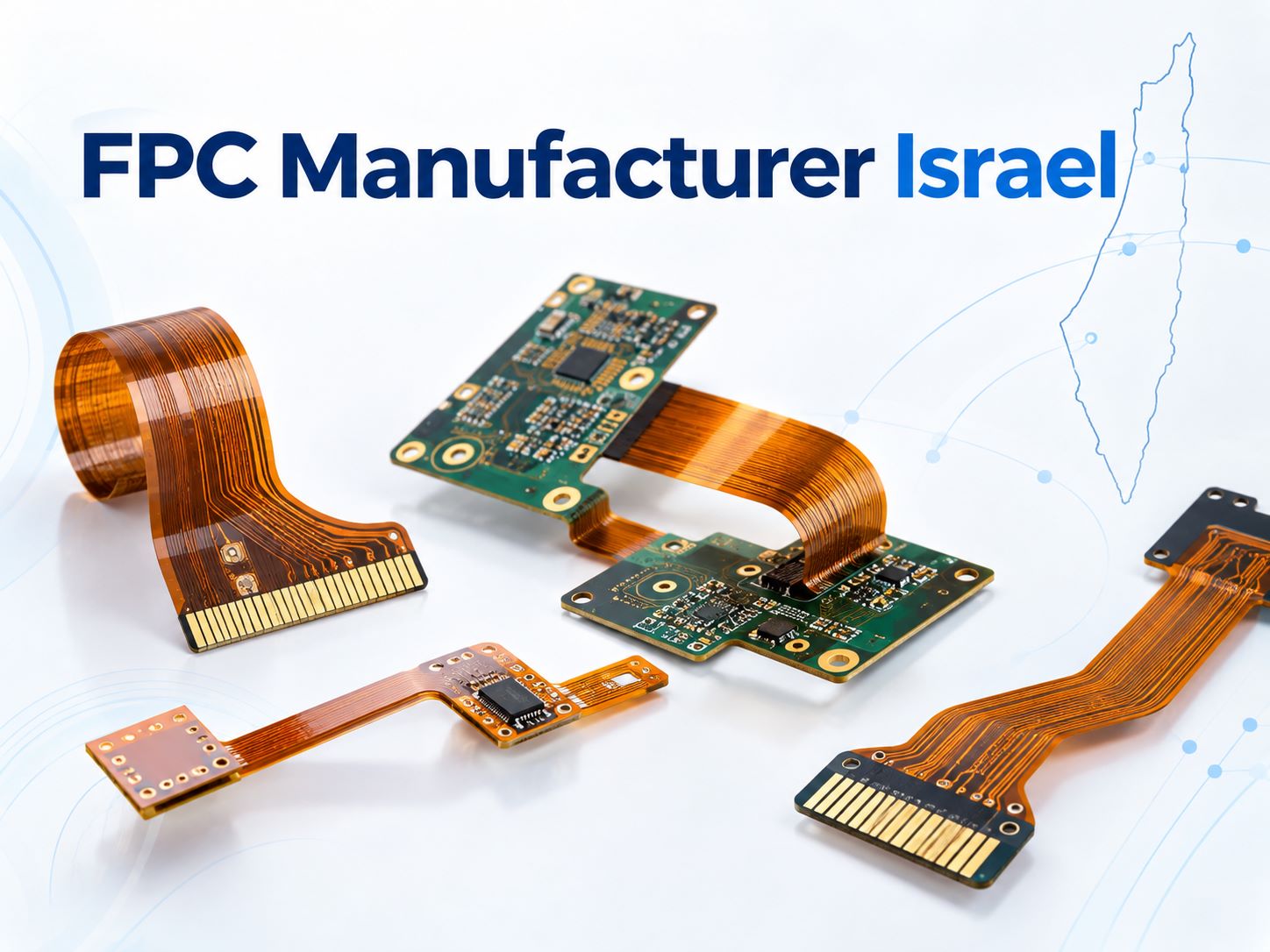
Searching for an FPC manufacturer Israel usually means the project has moved beyond basic flexible PCB research. Buyers now need to know who can manufacture the required flex construction, whether production must stay in Israel, how quickly prototypes can be delivered, and whether fabrication, component sourcing, assembly, and testing can be coordinated without adding more suppliers.

EBest Circuit is a China-based PCB and PCBA manufacturer serving Israeli customers rather than an Israeli domestic manufacturer. With 20+ years of PCB and PCBA manufacturing experience, we support FPC, rigid-flex, HDI, component sourcing, and downstream assembly for international projects. For Israeli programs that do not require local production, EBest provides another sourcing option to compare on process capability, quality systems, lead time, PCBA coverage, and repeat-production support.

FPC manufacturer Israel

Top 5 FPC Manufacturers in Israel to Compare

Israel has several established PCB companies supporting flexible and rigid-flex designs. Their strengths differ, so the following list is better treated as a supplier shortlist rather than an absolute quality ranking.

CompanyMain Strength
Eltek / NistecHigh-reliability flex and rigid-flex
Print ElectronicsFlex, rigid-flex, HDI
PCB TechnologiesAdvanced PCB + turnkey PCBA
TracePCBFlex prototypes and electrical testing
Ma’agalim D.S.PCB design, flex fabrication, assembly

Eltek / Nistec is particularly relevant for high-reliability flex and rigid-flex projects.

Print Electronics covers flexible PCB, rigid-flex, HDI, and other advanced constructions.

PCB Technologies combines PCB fabrication with PCBA and advanced packaging, which can be useful when a project needs broader manufacturing support.

TracePCB is relevant for prototype and lower-volume projects where engineering support and electrical testing matter.

Ma’agalim D.S. combines PCB design, fabrication, assembly, and turnkey support, including flex and rigid-flex projects.

The right supplier depends less on the company name than on whether its actual process capability fits the released FPC design.

FPC manufacturer Israel

What FPC Manufacturing Capabilities Matter for Israeli Projects?

For Israeli FPC projects, supplier fit can be judged quickly by comparing the released design with the factory’s actual production limits. EBest Circuit supports standard and advanced flexible PCB production with the following capabilities:

FPC CapabilityEBest Circuit
Layer count1–6 layers standard; up to 8 layers by review
Finished thickness0.06–0.60 mm
Maximum panel size240 × 780 mm standard; up to 240 × 1200 mm
Flex copper0.33–2 oz
Finished copperInner up to 2 oz standard / 3 oz special; outer up to 3 oz
Mechanical drillDown to 0.15 mm
Laser via3–4 mil standard; 2–3 mil special
PTH aspect ratio10:1 standard; up to 12:1
Minimum BGA pad10 mil standard; 8 mil special
Impedance tolerance±10%
Outline tolerance±0.10 mm
Surface finishENIG, hard gold, OSP, immersion tin, ENEPIG

Fine-line capability changes with copper thickness:

Finished CopperStandard Trace / SpaceSpecial Process
18 μm3 / 3 mil2.5 / 2.5 mil
35 μm4 / 4 mil3.5 / 3.5 mil
70 μm6 / 8 mil5.5 / 7 mil

EBest Circuit also supports adhesive and adhesiveless polyimide constructions, multiple coverlay options, and PI stiffeners for connector or reinforcement areas.

For projects requiring 8-layer FPC, 2–3 mil laser vias, fine-line routing, controlled impedance, heavier copper, or long-format flex, these limits provide a practical way to determine whether the design fits standard production or needs a special-process review.
FPC manufacturer Israel

How Is Flexible PCB Quality Controlled for Bending and Assembly?

Flexible PCB quality is not only about passing electrical testing. The board also has to survive handling, forming, assembly, and the bending conditions defined by the product.

For EBest FPC projects, quality control focuses on flex-specific risks:

  • Bend-area protection: vias, stiffener edges, copper transitions, and coverlay openings are reviewed around the bend zone.
  • Layer registration: copper and coverlay need to remain aligned around fine-pitch pads and connector areas.
  • Thickness control: finished flex thickness affects bend behavior and mechanical fit.
  • Stiffener accuracy: reinforcement must support the intended area without creating an unnecessary stress point.
  • Electrical continuity: flying-probe or fixture testing helps detect opens and shorts before assembly.
  • Assembly protection: flex sections can be supported during printing, placement, reflow, inspection, and handling.

When assembly is included, SPI, AOI, X-ray, ICT, or functional testing can be selected according to the component package and acceptance requirements.

The customer benefit is less risk of treating an FPC like a thin rigid PCB. Fabrication and assembly controls need to reflect how the circuit will actually bend and function in the finished product.

FPC manufacturer Israel

Which Certifications Matter for Flexible PCB Production in Israel?

The relevant certification depends on the final product. An industrial FPC, medical flex circuit, automotive sensor, and aerospace rigid-flex assembly may require very different supplier qualifications.

ApplicationCommon Qualification
General industrialISO 9001, IPC
MedicalISO 13485
AutomotiveIATF 16949
AerospaceAS9100D
Flex PCB workmanshipIPC-6013 / customer specification
Environmental complianceRoHS, REACH

EBest Circuit supports projects under ISO 9001, ISO 13485, IATF 16949, and AS9100D quality systems, together with applicable IPC, UL, RoHS, and REACH requirements.

These certifications should not be treated as a logo checklist.

For example, ISO 13485 may become a supplier-qualification requirement for a medical program, while AS9100D may be decisive for an aerospace sourcing plan. For a general industrial FPC, the approved material, IPC acceptance criteria, flex construction, traceability, and testing requirements may matter more.

The important question is whether the supplier’s quality system matches the actual project requirement.

How Fast Can FPC Prototypes and Production Orders Ship to Israel?

For standard EBest PCB projects, fabrication is commonly planned around 3–5 working days, with expedited options available for qualifying builds.

Flexible PCB lead time can change when the design includes:

  • special PI or adhesive systems;
  • uncommon copper thickness;
  • multilayer flex;
  • controlled impedance;
  • laser microvias;
  • tight stiffener tolerances;
  • special coverlay openings;
  • rigid-flex lamination;
  • additional testing.

For Israeli customers, the useful delivery date is not simply the number of days needed to fabricate the bare FPC.

A realistic schedule should consider:

engineering approval → material readiness → FPC fabrication → assembly/testing → shipment to Israel

This matters when comparing local production with an overseas supplier. Local manufacturing may shorten logistics, while an overseas route may offer broader capacity, different pricing, integrated PCBA, or better volume scalability.

The useful comparison is therefore the complete delivery schedule, not just the bare-board fabrication time.

Can One FPC Manufacturer Handle Flex PCB Assembly Too?

Yes. This can be particularly useful for flexible circuits because assembly and mechanical handling are closely connected to the FPC construction.

If fabrication and assembly are separated, the customer may need to coordinate:

FPC manufacturer → component supplier → SMT house → inspection/test provider

EBest Circuit can combine FPC fabrication, component sourcing, SMT/THT assembly, inspection, and agreed testing within the same project.

The customer gains:

  • Fewer supplier handoffs: less coordination between separate PCB and assembly vendors.
  • Better flex handling: fixtures and support methods can be planned around flexible sections.
  • Better stiffener coordination: connector and component areas can be reviewed together with assembly requirements.
  • Clearer BOM control: turnkey, partial-turnkey, and consigned sourcing are available.
  • One responsibility path: PCB-related assembly issues do not need to be negotiated between unrelated factories.

For overseas sourcing, combining FPC and PCBA is one of the clearest ways to reduce the extra coordination created by distance.

FPC Manufacturing Case Study for an Israeli Customer

A documented Israeli flex-related project involved a 10-layer rigid-flex industrial-control PCB.

ItemSpecification
Structure10-layer rigid-flex
Flex section4 flex layers
Flex thickness0.43 mm ±0.03 mm
Surface finishENIG
Via typeBlind vias
Impedance100 Ω differential

The manufacturing challenge was not simply producing a 10-layer PCB. The flex materials, rigid sections, blind vias, finished thickness, coverlay, and controlled impedance all had to remain aligned with the approved stackup.

EBest reviewed the construction as one manufacturing package before fabrication.

For the customer, the benefit was a controlled release before production instead of discovering stackup, impedance, or flex-construction differences after the rigid-flex boards had already been manufactured.

FPC manufacturer Israel

When Does an Overseas FPC Manufacturer Make Sense for Israeli Buyers?

An overseas FPC manufacturer only makes sense when the project is allowed to use overseas production.

A local Israeli supplier may be the stronger choice when:

  • the contract explicitly requires Israeli production;
  • defense or security rules restrict manufacturing location;
  • frequent face-to-face engineering support is necessary;
  • domestic logistics are part of the qualification plan.

An overseas supplier becomes more attractive when location is not mandatory and the buyer is comparing:

  • FPC or rigid-flex process capability;
  • prototype and production capacity;
  • component sourcing;
  • integrated PCBA;
  • material availability;
  • repeat-volume pricing;
  • certification coverage.

EBest Circuit serves Israeli customers from its Asian manufacturing base. It should therefore be evaluated as an overseas FPC and PCBA partner, not as an Israeli domestic manufacturer.

Why Choose EBest Circuit for FPC Projects in Israel?

For Israeli customers that can use overseas production, EBest Circuit is most useful when the project needs more than a basic flex PCB quotation.

Customers gain:

  • More FPC capability: 1–6 layers standard, special builds up to 8 layers, laser vias, controlled impedance, fine-line routing, and multiple PI construction options.
  • Fewer supplier handoffs: FPC fabrication, sourcing, PCBA, and testing can stay within one project.
  • Earlier flex-design review: bend areas, coverlay, stiffeners, vias, materials, and impedance are checked before production.
  • Better revision control: approved PCB data, BOM, assembly information, and substitutions remain aligned.
  • Support beyond prototypes: the approved manufacturing package can continue into repeat production.

EBest Circuit is a China-based PCB and PCBA manufacturer serving Israeli customers, not an Israeli manufacturer. If domestic production is mandatory, a qualified Israeli factory is the appropriate choice.

If overseas production is allowed, compare suppliers on FPC process fit, quality control, PCBA coverage, total lead time, and responsibility when the design or BOM changes rather than bare-board price alone.

FAQs About FPC Manufacturers in Israel

Are flexible PCBs manufactured in Israel?

Yes. Israel has local suppliers supporting flexible and rigid-flex PCB manufacturing. Buyers should still confirm the actual manufacturing site, technology coverage, PCBA scope, and any outsourced production steps.

What is the difference between FPC and flex PCB?

FPC stands for Flexible Printed Circuit and is commonly used interchangeably with flex PCB. Both refer to circuits built on flexible dielectric materials such as polyimide.

What materials are commonly used for FPC?

Polyimide is the most common flexible dielectric. FPC constructions may also use rolled or electrodeposited copper, adhesive or adhesiveless PI, coverlay, stiffeners, and different surface finishes.

Can an FPC manufacturer also assemble the board?

Yes. EBest Circuit can combine FPC fabrication with component sourcing, SMT/THT assembly, inspection, and customer-defined testing.

What affects FPC manufacturing lead time?

Layer count, PI material, copper thickness, coverlay, stiffeners, microvias, controlled impedance, surface finish, quantity, and assembly scope can all affect the schedule.

When should an Israeli buyer use an overseas FPC manufacturer?

Consider overseas production when domestic manufacturing is not mandatory and the project benefits from broader manufacturing capacity, integrated PCBA, component sourcing, special FPC processes, or repeat-volume production.

Ready to Start Your FPC Project?

If your search for an FPC manufacturer Israel has reached the quotation stage, send your Gerber files, stackup, fabrication drawing, BOM, CPL, assembly requirements, quantity, and target delivery date to sales@bestpcbs.com. EBest Circuit can review the flex construction, bend areas, materials, stiffeners, impedance, assembly requirements, and manufacturability before quotation.

You may also like

IMS PCB vs Ceramic Substrate: Which Should You Choose?

September 9th, 2026

IMS PCB vs ceramic substrate is not simply a contest between a low-cost board and a high-performance material. The right choice depends on where heat is generated, how it leaves the assembly, the required electrical isolation, the mechanical environment, and the cost of changing the surrounding design. This guide focuses on those practical consequences so you can identify the better starting point without paying for performance your product cannot use—or accepting risks that appear only after testing.

EBest Circuit supports both IMS PCB and ceramic substrate projects, allowing the discussion to begin with your application rather than a predetermined material. If you are comparing the two for a new design or a redesign, send your operating conditions and current construction to sales@bestpcbs.com. Our team can help you identify which option deserves deeper thermal, electrical, and mechanical validation.

IMS PCB vs ceramic substrate
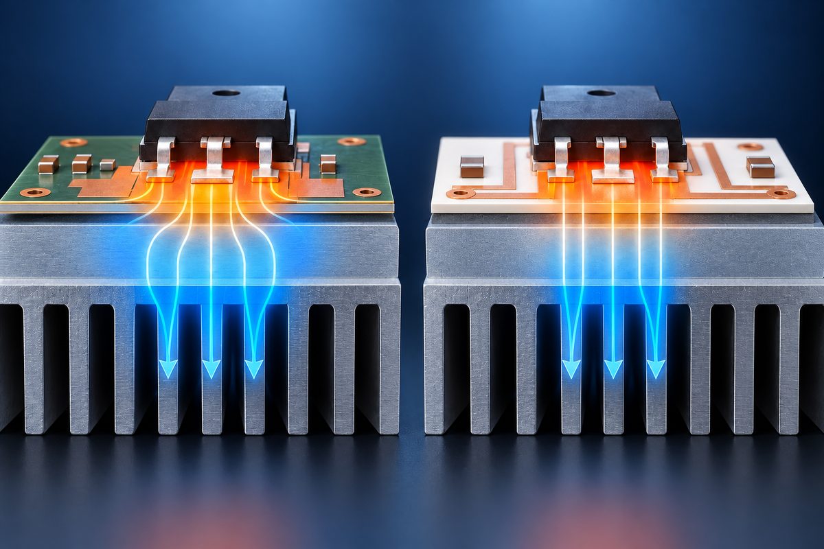
IMS PCB and ceramic substrate offer different thermal, electrical, mechanical, and cost advantages.

IMS PCB vs Ceramic Substrate: A Quick Comparison

An IMS PCB normally combines a copper circuit, a thermally conductive but electrically insulating dielectric, and an aluminum or copper base. A ceramic substrate uses a ceramic body—commonly alumina or aluminum nitride—as the insulating and heat-conducting foundation. Depending on the ceramic technology, conductors may be formed by thick film, thin film, DPC, DBC, AMB, or another metallization process.

The practical difference is that an IMS PCB moves heat through a thin polymer-based dielectric into a metal plate, while a ceramic substrate can provide insulation and heat transfer through the ceramic itself.

IMS PCB vs ceramic substrate
An IMS PCB uses a thin dielectric over a metal base, while a ceramic substrate uses the ceramic body as the insulating foundation.
Your priorityLikely starting point
Broad heat spreading at controlled costIMS PCB
High heat flux in a compact areaCeramic substrate
Resistance to vibration and handlingIMS PCB
High-temperature electrical stabilityCeramic substrate
Large board area or higher volumeIMS PCB
Compact power-device packagingCeramic substrate

This table is a starting point, not a final verdict. A well-designed IMS PCB can outperform an unsuitable ceramic construction at the system level, while ceramic may solve limitations that cannot be corrected by simply changing the IMS dielectric.

When Is an IMS PCB Enough—and When Should You Use a Ceramic Substrate?

An IMS PCB is often enough when the heat source is spread over a reasonable area, the metal base can connect efficiently to a heatsink or housing, and the required isolation can be achieved with a suitable dielectric. This is why IMS is widely considered for LED lighting, power conversion, automotive electronics, motor controls, and other products that need better heat removal than conventional FR-4 without moving to a ceramic platform.

Ceramic becomes more compelling when several demanding conditions occur together:

  • Heat is concentrated in a small footprint.
  • The assembly operates at elevated temperature.
  • High voltage and limited spacing reduce insulation margin.
  • Low thermal expansion or dimensional stability is important.
  • The substrate is part of a compact power module rather than a large standalone board.

The decision should not be based on power alone. A 100 W load distributed across a large IMS board is different from the same power concentrated under a small semiconductor. Heat-flux density, contact area, cooling method, voltage, and mechanical support are usually more informative than total wattage.

Ceramic should therefore be selected because it removes a known limitation—not simply because its material data sheet contains a higher thermal-conductivity number.

Will a Ceramic Substrate Actually Reduce Your Device Temperature?

It can, but only when the substrate is a meaningful part of the thermal bottleneck.

IMS PCB vs ceramic substrate
Substrate selection affects one part of the complete path from the power device to the heatsink.

In an IMS PCB, heat typically travels from the component into the copper, through the dielectric, into the metal base, and then through a thermal interface material to a heatsink or housing. The dielectric is thin, but its thermal conductivity is much lower than that of the surrounding copper and metal. When this layer dominates the thermal resistance, moving to an appropriate ceramic substrate may reduce the temperature rise.

However, changing the substrate may provide little benefit if the main restriction is elsewhere. Common examples include:

  • A poor component-to-pad thermal connection
  • Insufficient copper area around the heat source
  • A thick or poorly applied thermal interface material
  • An undersized heatsink
  • Limited airflow around the enclosure
  • High thermal resistance inside the semiconductor package

This is why comparing only material conductivity can be misleading. The useful comparison is the total junction-to-ambient thermal path under the same power, mounting pressure, cooling method, and available area.

Before changing materials, identify where the largest temperature drop occurs. If it is across the IMS dielectric, ceramic may offer a meaningful improvement. If it is between the metal base and the heatsink, improving that interface may deliver a larger result with less redesign.

Do You Need a Ceramic Substrate for Electrical Insulation?

Not every high-voltage design requires ceramic. An IMS PCB can provide electrical isolation when its dielectric material, thickness, conductor spacing, operating temperature, and manufacturing quality are appropriate for the application.

Ceramic becomes more attractive when the design needs insulation performance to remain stable under a combination of high voltage, high temperature, small dimensions, or long service life. Unlike an IMS construction, ceramic does not depend on a thin polymer dielectric between the copper and metal base. That structural difference can provide useful insulation and thermal advantages in demanding power-electronics environments.

The voltage printed on a material data sheet is not a complete design limit. Actual insulation performance is also affected by:

  • Dielectric or ceramic thickness
  • Conductor geometry and edge spacing
  • Surface contamination and humidity
  • Voids, cracks, or metallization defects
  • Repeated thermal and electrical stress
  • Creepage and clearance elsewhere in the assembly

If an IMS PCB already provides adequate isolation margin at the real operating temperature, ceramic may not add enough value to justify a platform change. If the design is losing insulation margin as voltage rises and spacing shrinks, ceramic deserves serious evaluation—but it must still be assessed as part of the complete assembly.

IMS PCB vs Ceramic Substrate: Which Handles Thermal Cycling and Stress Better?

Neither option is universally more reliable because they fail in different ways.

The metal base of an IMS PCB provides toughness and resistance to handling, vibration, and impact. This can be valuable in large boards, vehicle-mounted electronics, lighting assemblies, and products fastened directly to a housing. Its polymer dielectric can also accommodate some strain, although repeated temperature changes may stress copper features, solder joints, interfaces, and the bond between layers.

Ceramic offers excellent high-temperature stability and a coefficient of thermal expansion that may better match certain semiconductor materials. This can reduce stress in compact power assemblies. The trade-off is brittleness: unsupported ceramic can crack during machining, assembly, screw fastening, impact, or uneven mounting.

Customers should evaluate reliability against the real environment:

  • For vibration, impact, large dimensions, or frequent handling, the mechanical toughness of IMS may be valuable.
  • For high operating temperature and close integration with power semiconductors, ceramic may provide better material stability.
  • For either option, solder-joint life depends on the expansion mismatch among the substrate, copper, component, solder, and heatsink.

A reliability decision should therefore consider mounting and support conditions alongside the temperature range. Selecting ceramic for thermal reasons while clamping it like a metal board can introduce a new mechanical failure risk.

IMS PCB vs Ceramic Substrate: How Will Each Affect Layout and Assembly?

Changing the substrate can change more than the board material. It may affect routing, conductor formation, component attachment, panel size, mounting, inspection, and the way the finished assembly connects to its cooling structure.

An IMS PCB is often familiar to PCB designers and assemblers. It can support practical board sizes and conventional component assembly, although the metal base and insulation requirements influence drilling, routing, layer structure, and electrical clearances. More complex multilayer IMS constructions are possible, but they should not be treated as equivalent to standard multilayer FR-4.

Ceramic substrates can support compact, thermally demanding circuits and precise conductor technologies, but the selected ceramic process matters. Thick film, thin film, DPC, DBC, and AMB do not offer identical conductor thickness, feature size, bonding method, or cost. The word “ceramic” alone is not enough to define the design rules.

For the customer, the important issue is how far the material change spreads into the rest of the product. IMS usually fits more naturally into familiar PCB routing and solder-assembly workflows, especially when the circuit occupies a larger area. Moving to ceramic may allow a more compact power section, but the available conductor technology can change trace geometry, copper capability, component attachment, and panel utilization.

The mechanical design may change as well. An IMS board can often be fastened to a housing in a familiar way, while ceramic needs even support and controlled mounting pressure to reduce crack risk. The cooling interface must suit the new substrate rather than simply copying the previous stack. A platform change is worthwhile only when these layout and assembly changes produce a clear thermal, electrical, packaging, or reliability benefit in the finished product.

IMS PCB vs Ceramic Substrate Price: What Changes from Prototype to Production?

IMS PCB is usually the more economical starting point for larger boards and volume production because aluminum-base materials and familiar PCB processes are widely available. Ceramic substrates often cost more because the ceramic material, metallization, processing, dimensional control, and handling requirements can be more demanding.

But unit price alone can produce the wrong decision. A ceramic substrate may justify its cost when it enables a smaller power stage, removes a separate insulation component, creates enough temperature margin to avoid a larger cooling system, or supports longer service life at elevated temperature. In those cases, the substrate costs more but the complete product may become smaller, simpler, or more dependable.

Conversely, ceramic is difficult to justify when the product still requires the same large heatsink, enclosure, and board area while gaining little measurable improvement in temperature, insulation margin, or service life.

Prototype pricing can also exaggerate the difference. Small ceramic quantities may carry high setup and process costs, while production economics depend on substrate utilization, conductor technology, yield, inspection, and required tolerances. The useful question is not “Which board is cheaper?” but “Which complete product reaches the required performance and reliability at the lower total cost?”

IMS PCB vs Ceramic Substrate in Three Real Applications

The better option becomes clearer when the comparison is tied to a product rather than an isolated material property.

IMS PCB vs ceramic substrate
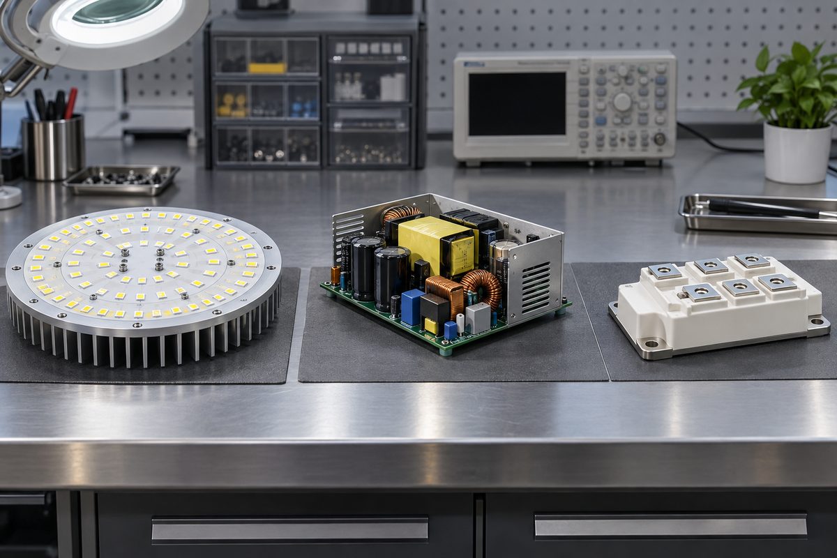
LED lighting, power conversion, and power modules place different demands on the substrate.

Application 1: Large LED lighting board

The heat sources are distributed across a relatively large area, the board attaches to an aluminum housing, and cost matters at production volume. An aluminum IMS PCB is usually the stronger starting point because it spreads heat, provides mechanical support, and integrates well with conventional LED assembly. Ceramic may not reduce LED temperature enough to offset the additional cost and fragility.

Application 2: Compact high-voltage power converter

The design combines concentrated heat, limited space, high voltage, and elevated operating temperature. A ceramic substrate becomes more attractive because thermal transfer and insulation can be provided within a compact structure. The conclusion still depends on package resistance, conductor requirements, creepage, cooling, and attachment method, but ceramic is more likely to solve a real design constraint here.

Application 3: Vehicle-mounted power electronics

The assembly experiences vibration, temperature cycling, mechanical fastening, and a demanding service life. IMS may be preferred when board area is moderate and mechanical toughness is critical. Ceramic may be selected for a compact power stage with high heat flux, but it needs suitable support and stress-controlled mounting. A hybrid architecture can also be sensible: ceramic for the high-density power section and IMS or another PCB technology for the broader circuit.

These scenarios show why application context matters. The same designer may reasonably select IMS for one product and ceramic for another without contradicting any material specification.

FAQs About IMS PCB vs Ceramic Substrate

Is a ceramic substrate always better than an IMS PCB?

No. Ceramic can provide stronger high-temperature, insulation, and localized thermal performance, but IMS often offers better mechanical toughness, larger practical board formats, familiar assembly, and lower production cost.

Can IMS PCB handle high-power components?

Yes, when the component footprint, dielectric, copper distribution, metal base, interface material, and cooling system create an acceptable total thermal path. Total power alone does not determine suitability.

Does aluminum nitride always outperform alumina?

Aluminum nitride generally offers higher thermal conductivity, but alumina may be adequate and more economical. Metallization, substrate thickness, geometry, interfaces, and the full cooling path still affect the result.

Can ceramic substrate replace an IMS PCB without changing the layout?

Not always. The conductor technology, design rules, substrate size, attachment process, mounting method, and thermal interface may require layout or mechanical changes.

What is the biggest risk when choosing between them?

The biggest risk is optimizing one material property while ignoring the complete product. A higher thermal-conductivity substrate cannot correct every package, interface, heatsink, insulation, or mechanical problem.

How should I compare the two for my project?

Begin with the problem the present design must solve. If the limitation is broad heat spreading, mechanical support, or production cost, IMS is often the logical baseline. If the limitation is concentrated heat, shrinking insulation margin, high operating temperature, or compact power packaging, ceramic deserves closer evaluation. The comparison becomes meaningful when it predicts a product-level result such as lower device temperature, more insulation margin, a smaller assembly, or longer service life.

If you are still deciding about IMS PCB vs ceramic substrate, describe the performance limit you are trying to overcome to sales@bestpcbs.com. EBest Circuit can help you compare realistic constructions and determine whether changing the substrate is likely to improve the finished product before you commit to a prototype.

You may also like

What Causes PCB Arcing and How Can You Prevent It?

September 9th, 2026

PCB arcing occurs when insulation between two conductive points breaks down and an ionized path carries current across air or along a surface. The visible flash may last only an instant, yet it can pit copper, melt solder, damage components, or carbonize the laminate. That carbonized path can lower the resistance between the same nodes and make another discharge easier to start.

The practical task is to find where the discharge traveled, what voltage actually appeared across that path, and why the insulation system could not withstand it. Those answers determine whether the correction belongs in the circuit, PCB layout, component selection, mechanical assembly, cleaning process, protective coating, or verification plan. A visibly charred board should remain de-energized until its damage and stored-energy hazards have been assessed.

PCB arcing between high-voltage conductors on a circuit board

What Is PCB Arcing, and What Happens When It Occurs?

PCB arcing is a high-current electrical discharge across a path that was intended to be insulating. It can jump through air between conductors, travel over a contaminated board surface, or connect a PCB node to a lead, connector shell, heatsink, screw, shield, or enclosure.

The discharge begins when the local electric field exceeds what the air, surface, or insulation system can withstand. Once a conductive plasma path forms, the current depends on the source impedance and available energy. A current-limited test source may produce a short flash; a low-impedance supply or charged capacitor can sustain the arc long enough to remove copper and damage the substrate.

Damage can continue after the first event:

  • Metal erosion: The arc can pit traces, connector pins, component leads, and solder joints, changing their current capacity and geometry.
  • Thermal damage: Local heat can melt solder, crack a package, delaminate the board, or ignite nearby material.
  • Carbonization: Burned resin can become partially conductive, creating a lower-resistance surface path for repeat tracking or arcing.
  • Circuit disturbance: A brief discharge can reset a processor, corrupt sensing, trip protection, or place an unexpected voltage on a low-voltage domain.
  • Hidden insulation loss: Damage may extend below a component or into the laminate even when the board powers up again.

The burn mark is therefore evidence of a failed insulation path, not a complete root-cause diagnosis. The initiating event may have been a transient, contamination, a loose connection, a layout feature, or a component failure that no longer exists after power is removed.

What Causes PCB Arcing?

PCB arcing occurs when voltage stress, insulation weakness, and available fault energy combine at one physical path. A cause analysis should separate five families because each one requires a different correction.

  • Electrical stress: Excessive working voltage, switching overshoot, inductive kickback, surge, hot-plug transients, transformer ringing, or motor regeneration can exceed the intended insulation level.
  • Layout and geometry: Insufficient clearance or creepage, sharp copper tips, exposed pads, closely spaced test points, board-edge copper, and copper beneath an isolation component can concentrate the field or shorten the path.
  • Environment: Condensation, conductive dust, salt, oil, and ionic residue can reduce surface resistance. Lower air density at altitude reduces air insulation strength and makes clearance more demanding.
  • Materials and protection: A laminate with unsuitable tracking resistance, damaged solder mask, voided coating, cracked potting, or aged insulation may no longer provide the assumed barrier.
  • Components and assembly: Wrong packages, long or bent leads, solder spikes, loose terminals, conductive hardware, contaminated connectors, and shifted components can defeat a correct nominal PCB gap.

The source also controls the outcome. The same weak path may create only leakage on a limited source but develop into destructive arcing when a capacitor bank, mains input, battery, or high-power converter supplies enough current. Root-cause work must identify both what initiated breakdown and what allowed the event to continue.

Why Can PCB Arcing Occur Even When the Nominal Voltage Seems Safe?

Nominal voltage can hide the peak differential voltage across the actual discharge nodes. PCB arcing responds to the instantaneous electric field, including transients and floating-node movement, rather than the number printed on the supply label.

A 48 V motor controller, for example, may expose a switching node to ringing or regenerative voltage well above the DC bus during braking. Opening a relay or interrupting current through an inductor can generate a short kickback pulse. Startup, shutdown, load dump, hot-plugging, and transformer leakage inductance can produce similar stress. A regulator input rated for the steady rail does not prove that every board gap sees only that rail voltage.

Measure the voltage between the two points that define the suspected arc path. Trace-to-ground measurements can miss a larger differential between two switching nodes, a node and a heatsink, or a primary-side conductor and a floating secondary assembly. Capture the relevant startup, shutdown, load, fault, and environmental states with probes and methods rated for the expected voltage and common-mode stress.

This distinction also explains why an unpowered resistance check may show no short. The initiating transient disappears when power is removed, and an air gap can read open until its breakdown voltage is exceeded. Conversely, carbonized damage may become more conductive with humidity or voltage even if a handheld meter does not reveal a hard short.

How Do Creepage and Clearance Affect PCB Arcing?

Clearance controls the shortest path through air, while creepage controls the shortest path along an insulating surface. Both must be evaluated because an assembly can have adequate copper-to-copper spacing in one view and still contain a shorter three-dimensional path.

Clearance may run from a trace to a component lead, connector shell, heatsink, shield, screw, standoff, or enclosure wall. Creepage can follow the board surface around a pad, along a slot wall, beneath a component, or across residue and coating. The copper gap shown in CAD is only one part of these paths.

The insulation function matters as much as the distance. Functional insulation keeps a circuit operating, while basic, supplementary, or reinforced insulation may protect against electric shock under specified conditions. The applicable product standard determines which insulation function is required and how working voltage, transients, pollution, materials, and altitude are applied.

For a practical review, mark voltage domains on the schematic and assembly, then inspect every boundary in three dimensions. Include tolerances, lead forming, solder fillets, component overhang, board movement, and conductive hardware. A connector or optocoupler package with inadequate pin spacing cannot be corrected by increasing only the adjacent PCB trace gap.

How Much PCB Spacing Is Needed to Prevent Arcing?

There is no universal PCB arcing distance based on voltage alone. The minimum spacing comes from the applicable end-product standard and the actual insulation conditions, not a general millimeters-per-volt rule.

The calculation or standards lookup needs these inputs:

  • Voltage waveform: Identify working voltage, repetitive peak voltage, transient level, frequency, and the exact two nodes under review.
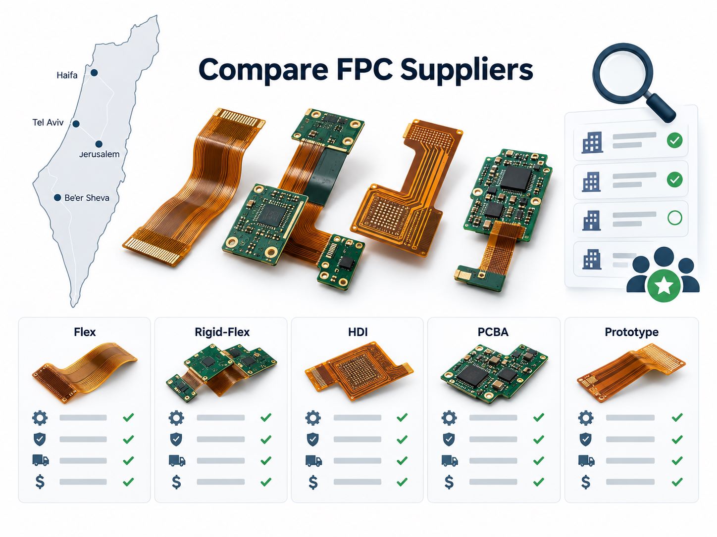
  • Insulation requirement: Define functional, basic, supplementary, or reinforced insulation and whether the path is part of a safety barrier.
  • Environment: Establish pollution degree, condensation risk, contamination control, and the maximum operating altitude.
  • Material behavior: Use the laminate material group or comparative tracking index where the governing method requires it.
  • Geometry and construction: Include the air path, surface path, slots, component packages, coating or potting system, and manufacturing tolerances.
  • Applicable standard: Use the product or system standard that governs the equipment; it may modify or add to the insulation-coordination method.

A PCB spacing calculator can help organize those inputs or retrieve a table value, but its answer is only as valid as the selected standard, categories, units, and waveform. Treat a calculator result as an engineering input to review, not as proof that the entire assembled product is safe.

Which PCB Layout and Component Features Increase Arcing Risk?

The highest-risk locations combine a short physical path with high differential voltage, field concentration, contamination exposure, or assembly variation. Review actual copper and hardware instead of relying only on a global design-rule check.

  • Sharp copper and exposed metal: Acute trace ends, pointed pours, narrow pad necks, test points, via rings, and solder spikes can concentrate the electric field.
  • Isolation-boundary copper: Planes, thermal copper, stitching vias, and unused pads under transformers, relays, optocouplers, or connectors may shorten the intended barrier.
  • Component leads and packages: Formed leads, terminal screws, relay pins, transformer windings, and power-device tabs can create paths that the bare-board spacing report does not include.
  • Ground and shield features: A ground pour can reduce the distance from a high-voltage node even when it improves EMI behavior elsewhere. Connector shells and shields may be grounded, floating, or transiently driven.
  • Mechanical hardware: Heatsinks, clips, mounting screws, standoffs, and enclosure walls can move within tolerance or collect contamination near a high-field node.
  • Board edges and slots: Copper too close to a routed edge, incomplete slot length, plating or burrs near a cutout, and conductive debris in a slot can reduce the real path.
  • Hidden assembly areas: Flux trapped beneath a component, solder balls, wire strands, metal swarf, and residue around through-hole leads can create an intermittent surface path.

Assign voltage-specific clearance rules where the EDA tool supports them, but finish with an assembly-level review. The relevant measurement is the shortest credible path after fabrication and assembly tolerances are applied.
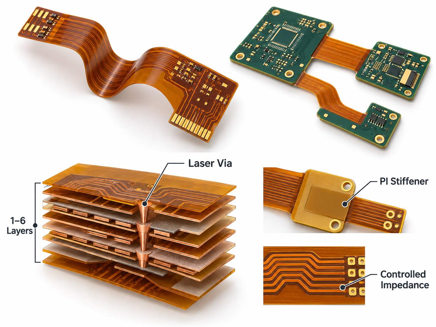
How Do Contamination, Humidity, Altitude, and PCB Materials Affect Arcing?

Environmental conditions can turn a board that passes a clean bench test into a field failure by weakening its air or surface insulation. The mechanisms differ, so the environmental correction must match the path.

Moisture alone does not automatically create an arc. The greater surface risk appears when moisture combines with ionic flux residue, salt, dust, or another contaminant. That film can lower surface resistance, allow leakage current, create local heating, and begin tracking. Repeated discharge can carbonize the laminate until the surface becomes a much easier path.

Condensation is more severe than a stable humidity percentage because it can form a continuous conductive film. Power cycling, cold starts, outdoor enclosures, washdown, and rapid temperature changes should therefore be considered even if room-temperature operation looks acceptable.

Altitude primarily reduces the strength of air insulation, so clearance may need correction as air pressure decreases. It does not automatically increase the physical creepage path, although the product environment can still change surface contamination and moisture behavior.

Material selection affects resistance to tracking. CTI or the corresponding material group may be an input to creepage requirements, but it does not replace clearance, cleanliness, or a suitable coating process. Solder mask is a process coating with openings and tolerances; it should not be credited as safety insulation unless the applicable construction and standard explicitly permit that use.

Field failures should be compared with the real service environment: contaminant type, cleaning history, humidity and condensation cycle, altitude, temperature, airflow, enclosure sealing, and maintenance. A dry, clean prototype test cannot represent all of those conditions.

Which Design Measures Can Help Prevent PCB Arcing?

The effective correction removes the verified initiating mechanism and preserves the insulation path after manufacturing and environmental variation. Adding a coating or slot without identifying that mechanism can leave the actual hazard unchanged.

  • Correct excessive voltage stress: Clamp inductive kickback, reduce switching overshoot and ringing, control hot-plug or surge energy, and confirm component ratings at the measured waveform.
  • Increase the relevant path: Increase clearance for an air path and creepage for a surface path. Remove unnecessary copper and keep high-voltage domains away from hardware, edges, connectors, and low-voltage circuitry.
  • Reduce field concentration: Round sharp copper features, avoid pointed pours and solder spikes, and reposition exposed high-voltage pads. Smooth geometry supplements adequate distance; it does not replace it.
  • Use slots for a defined purpose: A slot can lengthen a surface path and remove contaminated board material from that route. Its length, width, edge quality, tolerance, and relationship to component leads must be specified and inspected.
  • Control contamination: Match flux, cleaning, handling, drying, and cleanliness acceptance to the assembly and environment. Cleaning cannot restore carbonized laminate.
  • Apply coating or potting as a system: Select a material compatible with voltage, temperature, contamination, repair, and certification needs. Control coverage, thickness, cure, adhesion, bubbles, voids, cracks, and masked areas.
  • Coordinate fault energy: Fuses, current limiting, precharge, and protection can reduce damage after an arc starts. They do not create adequate insulation or prevent the first breakdown.
  • Lock the assembly geometry: Dimension connectors, formed leads, heatsinks, standoffs, screws, shields, and enclosure clearances so production tolerances cannot close the approved gap.

Approve each corrective measure against the identified arc path and a measurable acceptance condition. A larger gap does not correct switching overshoot, a transient clamp does not remove contamination, and coating does not restore carbonized laminate. The revised assembly should pass the voltage, environmental, insulation, and post-test inspection checks that correspond to the original failure mechanism.

How Can You Tell PCB Arcing From Corona, Tracking, or Electrical Breakdown?

Use the location, waveform, sound, residue, and material damage together because these mechanisms can overlap or evolve into one another. A black mark alone does not show which process occurred first.

Observed evidence Likely interpretation Next verification
Distinct strike path, pitted metal, melted lead, or heavy soot between conductive points A high-current arc crossed an air or surface path Reconstruct peak voltage, source energy, and the shortest three-dimensional path
Faint glow, hiss, ozone odor, or electrical noise near a high-field point without a complete bridge Corona or another partial discharge may be occurring Inspect sharp features and voids; use qualified partial-discharge methods when required
Dark branching marks or a glossy conductive trail along an insulating surface Surface tracking has developed through contamination or insulation degradation Check moisture, residue, material group, leakage path, and coating condition
Insulation no longer withstands the applied electric field, with or without a visible arc Electrical breakdown is the broader failure condition Identify whether the failed path is through air, along a surface, or through solid insulation
Scorched material remains conductive or the discharge repeats at a lower stress Carbonization has become a secondary fault path Remove the assembly from service and assess replacement rather than relying on cleaning

How Should You Troubleshoot a PCB After Arcing Occurs?

Troubleshooting should preserve evidence, identify the two discharge nodes, reconstruct the worst voltage event, and separate the initiating cause from secondary damage. Repeatedly energizing the board to watch it spark can enlarge the damage and expose the operator to hazardous energy.

  1. Make the assembly safe. Disconnect every source, control stored energy, verify the de-energized state with correctly rated equipment, and follow the product’s electrical-safety procedure.
  2. Preserve the failure evidence. Record board revision, serial or lot identity, operating state, load, supply, temperature, humidity, enclosure condition, protection response, odor, sound, and photographs before cleaning or removing parts.
  3. Identify both ends of the path. Inspect the board, component bodies, connector, heatsink, hardware, and enclosure with magnification. Look for pits, soot, melted metal, branching tracks, cracked coating, loose joints, and carbonized laminate.
  4. Reconstruct the electrical stress. Review startup, shutdown, switching, braking, hot-plug, surge, load changes, and fault behavior. Measure the suspected node-to-node waveform with qualified probes and a safe test method.
  5. Find the shortest credible route. Measure air and surface paths through the assembled geometry, including tolerances, leads, solder, slots, board edges, shields, screws, and movement.
  6. Separate cause from consequence. Decide whether spacing, a transient, contamination, loose metal, component failure, or insulation damage initiated the event. Treat carbonization as a new conductive path even if it began as a result.
  7. Define the disposition and correction. Replace a board when laminate, isolation barriers, inner layers, or safety-related spacing are damaged and cannot be restored and verified. Otherwise document the approved repair, design change, and required retest.

A board that powers up after cleaning is not automatically serviceable. Darkened resin may remain conductive below the surface, and an arc across a safety barrier can invalidate the insulation system even if the visible residue is removed.

How Can You Verify That a PCB Arcing Problem Has Been Solved?

Verification must reproduce the worst credible stress on the revised assembly and compare measurable results with acceptance criteria defined before the test. “No visible spark” during one nominal bench run is not sufficient.

  • Recheck the physical insulation paths: Measure the minimum clearance and creepage on the assembled product, including component leads, solder, coating boundaries, slots, hardware, enclosure parts, and tolerances.
  • Capture the worst voltage waveform: Verify working voltage, repetitive peaks, startup, shutdown, switching overshoot, braking, hot-plug, surge, load transients, and fault states at the actual nodes under review.
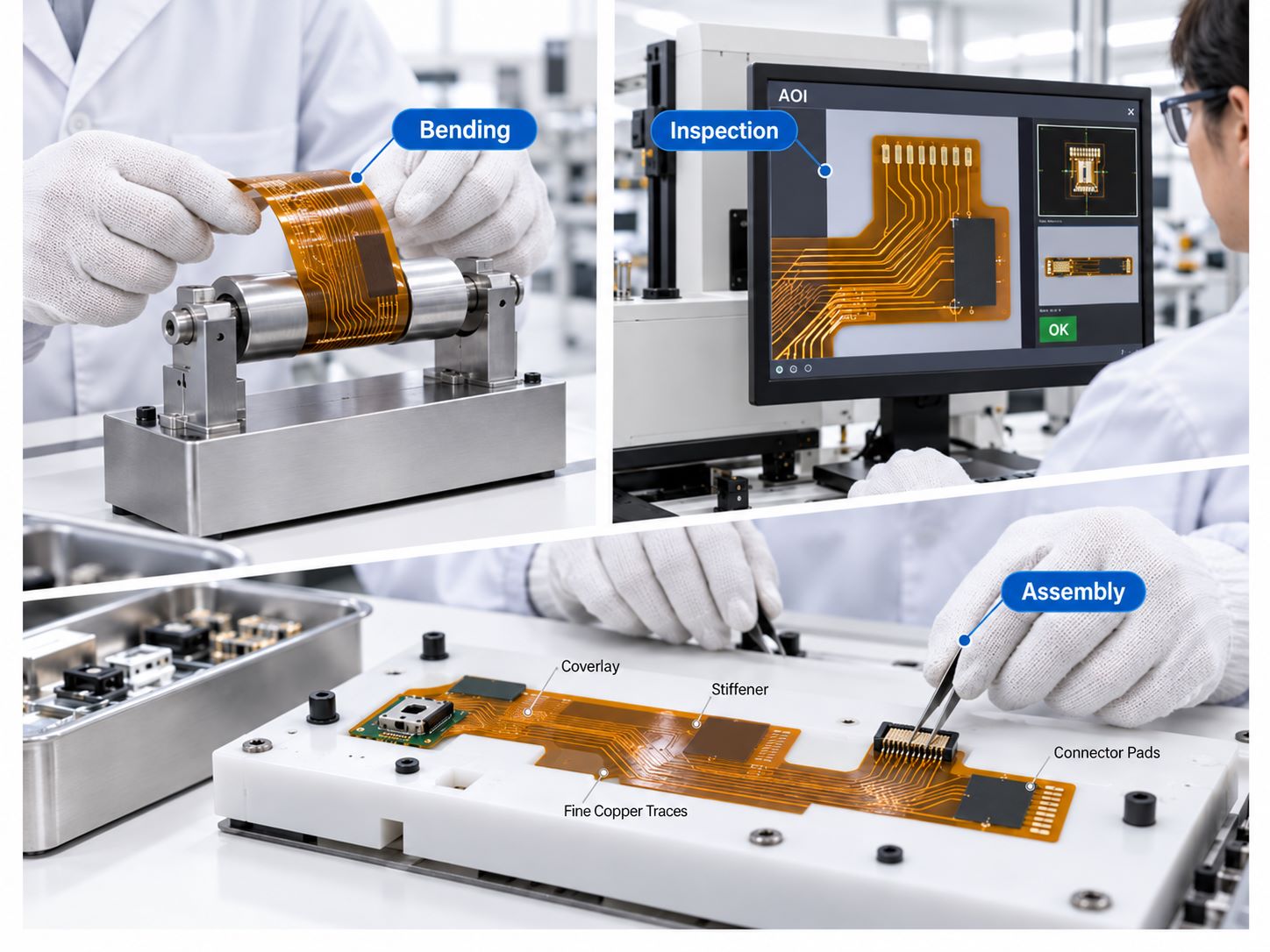
  • Reproduce the service environment: Apply the relevant temperature, humidity or condensation exposure, contamination assumptions, altitude, vibration, and enclosure condition rather than relying only on a clean laboratory state.
  • Use the required insulation tests: Perform insulation-resistance, dielectric-withstand, leakage, or partial-discharge testing when the applicable standard and insulation design require them. Define nodes, level, waveform, ramp, duration, limits, and safe failure response.
  • Test more than the repaired sample: Use a justified sample plan that can reveal tolerance, assembly, coating, cleanliness, component, and lot variation. A hand-selected prototype cannot prove production control.
  • Inspect after electrical stress: Look for new pits, discoloration, tracking, coating cracks, leakage change, abnormal sound, ozone, or thermal damage even when the circuit continues operating.
  • Freeze the verified configuration: Record schematic and PCB revision, stackup, materials, exact components or approved alternates, manufacturing site, coating process, firmware or load state, test setup, results, and acceptance decision.

Any change that affects voltage stress or the insulation path requires impact review. Substituting a relay, connector, transformer, coating, laminate, heatsink, screw, or assembly process can invalidate an earlier result without changing the nominal circuit function.
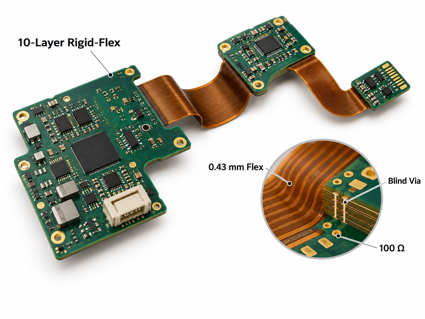
For fabrication or assembly review, send the voltage-domain drawing, working and transient voltages, applicable insulation requirement, environment, stackup, material or CTI requirement, Gerber or ODB++, drill and route data, slots, BOM, assembly drawing, coating or potting specification, quantities, target schedule, failure evidence, and acceptance tests. EBest Circuit can use that controlled data for a free DFM review and quotation discussion. Send the files and requirements to sales@bestpcbs.com.

FAQs About PCB Arcing

Q1: Can a PCB arc even if a multimeter shows no short after power is removed?

A1: Yes. An air gap normally reads open until voltage exceeds its breakdown condition, and a transient may disappear when the circuit is unpowered. Carbonized or contaminated material can also behave differently with humidity, voltage, and temperature. Use the physical evidence and the actual energized node-to-node waveform; do not repeatedly power a damaged board to force the fault to reappear.

Q2: Does DC arc differently from AC on a PCB?

A2: Yes. AC has repeated current zero crossings that may help an arc extinguish, whereas DC has no natural zero crossing and may sustain current when the source can support it. Initiation and damage still depend on peak voltage, path geometry, contamination, source impedance, polarity, switching behavior, and protection. Apply the standard and test method for the actual waveform.

Q3: Can an arc jump from a PCB to a heatsink or metal enclosure?

A3: Yes. A heatsink, screw, standoff, shield, connector shell, or enclosure wall may be the closest conductor. Its voltage can be grounded, floating, or capacitively driven, so measure the potential difference and clearance to the real metal part across assembly tolerances.

Q4: Can PCB arcing start underneath a component?

A4: Yes. Hidden copper, solder residue, a voided coating, long leads, thermal pads, or contamination can create a shorter path under relays, transformers, connectors, optocouplers, and power devices. Inspect beneath the suspect package and verify the package’s own pin and body insulation distances.

Q5: Will a fuse prevent PCB arcing?

A5: A fuse may limit the duration or energy of a sustained fault, but it does not prevent insulation from breaking down. The arc current may also be too low or too brief to open the fuse promptly. Coordinate protection with spacing, transient control, materials, source impedance, and the required safe-failure behavior.

Q6: Can an arcing PCB be cleaned and returned to service?

A6: Cleaning may remove conductive residue when the laminate and insulation system remain undamaged, but it cannot reverse carbonization, delamination, cracked insulation, or eroded conductors. Replace the board when the damage reaches a safety barrier or cannot be fully inspected and verified. Any permitted repair needs an approved process and the same acceptance tests required for a conforming assembly.

Q7: Can conformal coating replace creepage and clearance?

A7: Not by default. Coating can protect a clean, compatible assembly from moisture and contamination, but missed areas, bubbles, pinholes, cracks, poor cure, and rework can create weak paths. Credit coating as insulation only when the applicable standard, material system, process control, inspection, and qualification support that use.

You may also like

EV Charger MCPCB Manufacturer | Custom Fabrication & Assembly

September 8th, 2026

An EV charger MCPCB helps move heat away from switching devices, rectifiers, power resistors, and auxiliary power circuits as charging systems become smaller and more powerful. An MCPCB can move that heat into a chassis, heat sink, or cold plate more efficiently than a conventional board—but only when the board is designed as part of that thermal path.

EBest Circuit manufactures custom aluminum- and copper-base PCBs and provides component sourcing, assembly, and testing. We help charger developers match the board construction to the module instead of treating every PCB inside an EV charger as a metal-core board.

EV charger PCB is a broad term. EV charging PCB and electric vehicle charging PCB can refer to several different boards across the charging system. In this article, EV charger MCPCB means a metal-core board used within a defined power or thermal module—not every PCB in the system.

EV charger MCPCB

Where Does an MCPCB Fit Inside an EV Charger?

An MCPCB fits where heat is concentrated and there is a short, controlled path from the component to a metal cooling surface.

In an EV charger, that can include a compact power conversion board, a rectifier section, an auxiliary power module, or a board carrying high-loss switching devices. It can also be used for high-power status lighting. The metal base spreads heat beneath these components and transfers it toward the charger housing, a heat sink, or a cold plate.

It is usually not the first choice for communication, metering, display, or central control boards. Those boards often need multilayer signal routing, controlled impedance, dense interconnections, or isolation between several electrical domains. FR-4, heavy-copper PCB, insulated metal substrate, ceramic, and hybrid structures each solve different problems.

Application labels also need clear boundaries. An EVSE PCB belongs to stationary charging equipment, while an on-board charger PCB, or OBC PCB, operates inside the vehicle. A DC fast charging PCB may describe a control board, gate-driver board, or power-module board with very different construction needs. An EV charger control board is usually not an MCPCB unless it also carries concentrated heat into a defined cooling surface. Supplier listings may use the phrase EV charging board PCB, but that wording is too broad to specify the correct board technology.

The practical dividing line is simple:

  • Use an MCPCB when the PCB must conduct heat into a defined cooling surface.
  • Consider another construction when routing density, high-voltage spacing, or complex multilayer connections dominate the design.

That distinction keeps the thermal board focused on the part of the charger where it creates measurable value.

When Does EV Charger PCB Design Require a Metal Core?

Choose a metal core PCB for EV charging when temperature cannot be controlled reliably through copper area, thermal vias, airflow, and a conventional laminate alone.

This often happens when several conditions appear together: high component loss, limited board area, restricted airflow, and direct mechanical contact with a heat sink or enclosure. In that situation, the metal base becomes a heat-spreading layer rather than simply a stronger board material.

For example, a power semiconductor may operate safely on FR-4 at a moderate load but exceed its temperature target when the same circuit is packaged into a smaller charger. Moving to an MCPCB can shorten the heat path. The result depends on the entire structure—from the component pad and copper circuit through the dielectric layer and metal base to the external cooling surface.

A metal core is less useful when the main limitation is elsewhere. It will not correct an undersized heat sink, poor board-to-housing contact, excessive semiconductor loss, or insufficient airflow. It may also complicate a design that needs many signal layers or long high-voltage creepage paths.

The choice should therefore be based on the module’s losses, allowable temperatures, mechanical interface, and insulation requirement—not on charger power alone.

Which PCB Material Fits Your EV Charger Application?

The right material depends on the job of the board. An EV charger normally uses more than one PCB technology because heat transfer, current carrying, signal routing, isolation, and mechanical requirements do not peak in the same place.

  • Aluminum MCPCB fits cost-sensitive thermal modules that need to spread component heat into a housing or heat sink. It is a practical choice when the layout is relatively simple and aluminum can keep the hot spots within the temperature target.
  • Copper-base MCPCB fits smaller or more demanding thermal modules where heat is highly concentrated and stronger lateral heat spreading is needed. It can improve the path away from a power device, but it also increases material cost and board weight.
  • High-Tg FR-4 fits control, communication, sensing, and multilayer power-control boards that need routing density, plated through-holes, and high-voltage separation. Its higher glass-transition temperature improves dimensional and thermal stability, but High-Tg does not mean high thermal conductivity.
  • Heavy-copper PCB fits high-current distribution, terminals, relays, and power paths where conductor temperature rise is the main concern. It carries more current and adds thermal mass, but it does not provide the same direct board-to-heat-sink path as an MCPCB.
  • Ceramic PCB fits compact modules that need strong electrical insulation, high-temperature stability, low expansion, or high thermal performance. It can be valuable around demanding power devices, but cost, size, brittleness, copper attachment, and assembly handling must be considered.

Many chargers need a mixed solution rather than one material throughout the product. For example, a High-Tg FR-4 control board can manage communication and safety functions, a heavy-copper board can distribute current, and an aluminum, copper-base, or ceramic board can support the most concentrated thermal load.

Use the dominant engineering problem as the first filter:

  • heat must move into a chassis or heat sink → aluminum or copper-base MCPCB;
  • high current must travel across the board → heavy-copper PCB;
  • multilayer signals and isolation dominate → High-Tg FR-4;
  • high temperature, insulation, and dimensional stability dominate → ceramic PCB.

Final selection still depends on operating voltage, loss distribution, cooling design, board size, production quantity, and target cost. A material comparison is useful only when it is tied to the actual EV charger module.

EV charger MCPCB

What Thermal Management Risks Should Be Checked in an EV Charger MCPCB?

The main risk is assuming that a high thermal-conductivity material automatically produces a cool, reliable assembly. Heat must cross several interfaces, and the weakest one can control the result.

  • A thick dielectric layer can restrict heat flow. It may provide stronger isolation, but it also increases thermal resistance. The correct balance depends on operating voltage and heat density.
  • A high average board temperature can hide local hot spots. Temperature should be checked beneath the switching device and at its thermal pad, not only at the edge of the board.
  • Poor contact can cancel the benefit of the metal base. Board flatness, interface material, screw position, mounting pressure, and heat-sink finish affect real performance.
  • Copper geometry affects both current and temperature. Narrow current paths, connector transitions, or insufficient copper around a power device can create additional heat before it reaches the base metal.
  • Thermal cycling creates mechanical stress. Different expansion rates among components, solder joints, copper, dielectric, and metal base can reduce long-term reliability.
  • Electrical isolation cannot be traded away for lower thermal resistance. Dielectric withstand, creepage, and clearance remain essential in charger hardware.

A useful thermal review follows the heat from its source to the final cooling surface. It does not stop at the MCPCB datasheet value.

What Should Buyers Specify for DC Fast Charging Boards?

For DC fast charging, buyers should first specify the function of the board. A control PCB, gate-driver board, power module, and communication board experience different voltage, current, heat, and isolation conditions.

For the MCPCB itself, the most influential requirements are:

  • operating and peak current;
  • voltage and dielectric withstand requirement;
  • expected component losses and hot-spot locations;
  • aluminum or copper base;
  • dielectric thickness and thermal performance;
  • copper weight and critical current paths;
  • finished thickness, flatness, and mounting tolerances;
  • connection to the heat sink, housing, or cold plate;
  • operating environment and temperature range.

These details matter more than requesting the “highest thermal conductivity.” A thinner dielectric may improve heat transfer but must still meet isolation needs. A copper base may spread heat effectively but can add unnecessary cost and weight if an aluminum base already meets the temperature target.

Buyers should also define whether the order covers bare boards or completed assemblies. If components, thermal interface materials, busbars, connectors, or heat sinks are part of the build, they should be considered together because they change the assembly process and final thermal path.

How Should EV Charger PCB Assembly Be Qualified?

An EV charger PCBA should be qualified by proving that the assembled module performs as intended under representative electrical, thermal, and mechanical conditions. This is the practical purpose of EV charger PCB assembly qualification.

Start with the failures that matter to the product. A power board may need confirmation of current handling, isolation, temperature rise, and solder integrity. A module attached to a housing may also need verification of flatness, contact pressure, connector alignment, and repeated thermal cycling.

Inspection methods should match the assembly:

  • AOI can verify polarity, placement, and visible solder joints.
  • X-ray can examine solder beneath power packages and thermal pads.
  • Electrical tests can check continuity, isolation, and withstand performance.
  • Functional testing can confirm that the module operates at its intended load.
  • Temperature measurements can reveal whether heat reaches the cooling surface without an excessive local hot spot.

The prototype should be tested in a realistic mechanical setup. Testing a loose board on a bench cannot represent a design that relies on a chassis or cold plate. Once the module passes, the approved material, stack-up, component revision, mounting method, and test limits should remain consistent for repeat production.

EV charger MCPCB

How Do You Choose an EV Charger Circuit Board Manufacturer?

Choose an EV charger PCB manufacturer that understands both sides of the project: how to build the metal-core board and how that board functions inside the charger.

A capable supplier should be able to explain why the proposed base metal, dielectric, copper weight, surface finish, and assembly process fit the module. If a different PCB construction would serve the application better, the supplier should identify that before production rather than simply quoting the requested material.

Coordination also affects the result. When bare-board fabrication, component sourcing, assembly, and testing are handled separately, a thermal or soldering issue can fall between suppliers. A coordinated PCB and PCBA workflow makes it easier to connect material decisions with component packages, solder profiles, mechanical interfaces, and acceptance tests.

EBest Circuit supports prototypes, small batches, and repeat production through PCB manufacturing, component sourcing, PCBA, and testing. One business contact works with an engineering support team to coordinate technical questions. DFM review can identify conflicts involving the board structure, component spacing, panelization, assembly access, and testability before the build begins.

For programs that require formal quality controls, available certifications include ISO 9001, ISO 13485, IATF 16949, and AS9100D. The applicable production site, documentation, inspection level, and customer requirements should be confirmed for the individual project.

The strongest manufacturing partner is the one that reduces uncertainty before the prototype and preserves the approved solution when the project moves into repeat production.

Why Choose EBest Circuit as Your EV Charger Circuit Board Manufacturer?

EBest Circuit gives EV charger developers one coordinated route from a thermal-board concept to an assembled and tested product. Instead of separating the bare board, components, assembly, and engineering questions among several suppliers, customers work with one business contact supported by three engineers throughout the project.

This is especially useful for an EV charger MCPCB because the board material cannot be separated from the power package, solder joint, mounting surface, and cooling structure. Our engineering support connects these decisions before production:

  • DFM review covers the MCPCB structure, dielectric, copper, tolerances, panelization, component spacing, and test access.
  • PCB fabrication, component sourcing, PCBA, and testing can be managed as one project.
  • Prototype and small-batch support helps engineers check electrical operation, mechanical fit, and thermal behavior before repeat production.
  • A supply network of more than 1,000 partners supports component and material sourcing while our own PCB and PCBA factories coordinate production quality and timing.
  • Digital production records allow material and product batches, manufacturing progress, and production history to be traced quickly.

EBest Circuit has 20 years of PCBA experience and has served more than 10,000 engineers and 1,800 customers. Available quality-system certifications include ISO 9001, ISO 13485, IATF 16949, and AS9100D. The applicable factory, inspection plan, documentation, and certification requirements are confirmed according to the individual EV charging project.

For customers, the practical benefit is a shorter path from an engineering question to a build decision—and fewer gaps between MCPCB fabrication, assembly, thermal integration, and testing.

FAQs About EV Charger MCPCB

Does every EV charger need an MCPCB?

No. An EV charger may contain several board types. MCPCB is most suitable for a board that must transfer concentrated component heat into a metal cooling structure.

Is aluminum or copper better for an EV charger MCPCB?

Aluminum is often sufficient for cost-effective heat spreading. Copper can spread heat more aggressively but adds cost and weight. The right choice depends on losses, board size, cooling design, and temperature targets.

Does higher thermal conductivity always produce a cooler board?

No. Dielectric thickness, copper layout, component attachment, interface material, mounting pressure, and the external heat sink can have as much influence as the published conductivity value.

Can one supplier manufacture and assemble the board?

Yes. Combining fabrication, component sourcing, PCBA, and testing can reduce handoff risks, especially when power packages, thermal pads, heavy connectors, or a defined cooling interface are involved.

What should a prototype prove?

It should prove electrical operation, isolation, temperature behavior, solder quality, mechanical fit, and contact with the intended cooling surface under representative conditions.

Can an approved prototype move directly into repeat production?

It can move forward after the material, stack-up, components, assembly method, mechanical interface, and acceptance limits are frozen. Any later substitution should be reviewed for electrical, thermal, and mechanical impact.

Need a custom EV charger MCPCB for a power or thermal module? Send your Gerber files, BOM, board drawing, operating conditions, quantities, and testing needs to sales@bestpcbs.com. EBest Circuit can review the construction and provide a coordinated fabrication and assembly quotation.

You may also like

Where Can You Find a Reliable Heavy Copper PCB Manufacturer in Israel?

September 8th, 2026

Buyers comparing heavy copper PCB manufacturers in Israel can approach verified Israeli fabricators, Israel-based engineering and sourcing providers, or qualified overseas factories. PCB Technologies and Eltek publicly identify PCB manufacturing operations in Israel and describe thick-copper or heavy-copper capability. APEX PCB and Ma’agalim D.S. are useful Israel-based contacts, but buyers should confirm which factory will manufacture each order.

The purchasing decision should follow a clear sequence: identify realistic suppliers, check whether the relevant factory has suitable certifications, compare the complete process capability, verify quality evidence, and then normalize price, lead time, and supply terms. This prevents a local address, a broad “heavy copper” claim, or a low quotation from being mistaken for a qualified manufacturing solution.

heavy copper PCB manufacturers in Israel, heavy copper power board under inspection on an electronics workbench

Which Heavy Copper PCB Manufacturers Are Available in Israel?

Buyers evaluating heavy copper PCB manufacturers in Israel can begin with two verified Israeli fabricators and two Israel-based engineering or sourcing providers. Separating these roles at the shortlist stage shows who is responsible for fabrication and which companies require further confirmation of the production site.

Company Address Services Process capabilities Lead time Advantages
PCB Technologies 7 Ahoman St., Migdal-HaEmek, Israel, as stated on its published site certificate PCB fabrication, PCB assembly, testing, inspection, rework, NPI, and offshore coordination Multilayer high-reliability PCBs, thick copper, embedded copper, via farms, thermal management, HDI, rigid-flex, and prototype through low- or mid-volume production Project-specific; confirm after DFM, material review, capacity allocation, inspection scope, and the selected local or offshore route Israeli fabrication identity with PCB and PCBA support; useful when the project needs close engineering coordination across board, assembly, and thermal requirements
Eltek 20 Ben Zion Gelis St., Petach Tikvah 4927920, Israel High-reliability PCB engineering and in-house fabrication, with global sourcing available for additional production routes Heavy-copper multilayers, HDI, rigid, flex, rigid-flex, RF and microwave, special materials, and high-reliability constructions Project-specific; confirm the quick-turn slot, material availability, engineering-release date, tests, and whether Eltek or a sourcing partner will build the order Direct access to an Israeli high-reliability manufacturer; relevant when aerospace, defense, medical, RF, or complex multilayer controls influence qualification
APEX PCB Kibbutz Hazorea 3658100, Israel Local technical support and PCB sourcing through a global supplier network Published heavy-copper range above 70 µm up to 204 µm, plus multilayer, rigid-flex, HDI, IMS, and high-frequency PCB options Project-specific; depends on the assigned factory, material, stackup, quantity, inspection, international transport, and customs Israeli point of contact with access to multiple production options; useful when local coordination is needed and the actual factory remains transparent
Ma’agalim D.S. 22 Maskit St., Herzliya 46733, Israel PCB layout, fabrication sourcing, assembly, simulation, panelization, and turnkey project coordination High-Tg heavy-copper foil, multilayer, HDI, rigid-flex, metal-base and mixed-dielectric boards, microvias, blind or buried vias, and specialized routing Project-specific; confirm the production factory, engineering-release point, material plan, inspection scope, and delivered date in Israel Combines local design and project support with fabrication and assembly coordination; useful when one contact must manage several engineering stages

The shortlist is ready only when each company’s role, production address, capability scope, and delivery basis are clear. The next filter is whether the factory’s certificates cover the site, process, and end market required by the project.

What Certifications Should You Check When Choosing a Heavy Copper PCB Manufacturer?

Use certification as the first qualification filter by matching the standard to the product and the certificate to the factory that will build the board. Check the legal entity, address, scope, issuing body, certificate number, and validity dates before accepting any certification claim.

  • ISO 9001: This is a general quality-management baseline covering controlled processes, records, corrective action, and continual improvement. Confirm that the certificate scope includes PCB fabrication or the operation being purchased.
  • IATF 16949: This may be relevant for automotive supply chains that require automotive quality planning, traceability, change control, and defect-prevention systems. Do not request it merely because the board carries high current; its relevance comes from the customer and product program.
  • ISO 13485: Medical-device projects may require a quality system designed for regulated medical manufacturing. Check whether the certificate covers the responsible facility and whether the supplier can meet the project’s traceability and change-control requirements.
  • AS9100: Aerospace and defense programs may require aerospace quality controls in addition to technical PCB capability. Confirm the certified entity, site, scope, and any customer-specific approval before relying on the claim.
  • UL recognition and material compliance: If the design or market requires a UL-recognized PCB construction, RoHS, REACH, or another material declaration, identify the exact requirement in the RFQ. General corporate compliance language does not prove that the released stackup is covered.

A valid, relevant, site-specific certificate allows a supplier to move into technical evaluation; it does not approve the board itself. The next step is to compare whether that certified factory can manufacture the full copper, stackup, geometry, hole, material, and finish combination.

What Heavy Copper PCB Capabilities Should You Compare?

Compare the complete manufacturable feature combination, not the largest copper weight printed on a capability page. Two factories may both advertise 6 oz copper while accepting very different layer counts, finished holes, spacing, materials, or board thicknesses.

  • Base and finished copper by layer: State inner- and outer-layer requirements separately. Outer layers normally gain copper during plating, so the starting foil and finished value are not interchangeable. Ask the supplier to mark both values on its proposed stackup.
  • Layer count and mixed copper construction: Confirm whether the requested copper can be combined with the total layer count, dielectric structure, overall thickness, and lighter signal layers. Mixed weights can affect etching, resin fill, registration, lamination, and warpage.
  • Minimum trace and spacing: Heavy copper requires more etching allowance and changes the achievable conductor profile. Submit the actual narrowest features and copper clearances instead of relying on a standalone minimum value.
  • Finished holes and current transitions: Define drilled size, finished size, via structure, barrel-copper requirement, via quantity, and current through each transition. A broad surface conductor can still be limited by a narrow neck, connector pad, or insufficient plated-hole copper.
  • Material and board thickness: Confirm the laminate family, Tg or other required properties, dielectric thicknesses, thermal constraints, overall thickness tolerance, and dimensional limits. A listed material may not be available with every heavy-copper construction.
  • Surface finish and solder mask: Check whether the selected finish, mask thickness, color, clearance, and assembly interface are compatible with the copper topography and end-use environment.
  • High-current design inputs: Provide conductor width and length, continuous and peak current, duty cycle, allowable temperature rise, ambient conditions, airflow, heat sinking, and terminal limits. The factory reviews manufacturability; the product team remains responsible for validating electrical and thermal performance.

A meaningful capability comparison uses the same released construction for every supplier and records all accepted limits or required changes. Once manufacturability is confirmed, the buyer must verify whether the chosen process can repeatedly produce boards that meet the approved requirements.

How Can You Check a Manufacturer’s Heavy Copper PCB Quality?

Ask each qualified supplier to show how it will verify copper thickness, plated holes, materials, dimensions, electrical integrity, and lot release. Defining these records before quotation makes quality measurable and exposes any inspection gaps before production begins.

  • Copper-thickness verification: Agree on how inner copper, finished outer copper, and relevant plated features will be measured. For critical designs, request traceable coupon or microsection results tied to the correct part number, revision, panel, and production lot.
  • Plated-through-hole evaluation: Specify finished-hole dimensions and the applicable barrel-copper or workmanship requirement. A microsection can show plating distribution, voids, hole-wall condition, and the relationship between the drilled feature and finished result.
  • Material traceability: Request laminate, copper foil, surface-finish chemistry, date code, lot identity, and certificate-of-conformance records appropriate to the project. Verify that the received records identify the shipped revision and quantity.
  • Dimensional inspection: Define critical board dimensions, overall thickness, slots, hole locations, cutouts, and tolerances. Ask whether the supplier will provide first-article measurements or a lot inspection report for the characteristics that affect fit or current-path assembly.
  • Electrical testing: State continuity, isolation, netlist, impedance where applicable, and any special high-current or functional test that must be performed. The report should identify the test method, coverage, revision, and acceptance result.
  • First-article and lot release: Use a controlled first build to verify fit, assembly, current path, temperature rise, and product operation. Transfer all approved changes into the fabrication data, stackup, BOM, inspection plan, and test instructions before repeat production.
  • Nonconformance and change control: Agree on notification, containment, root-cause response, rework approval, and authorization for factory, material, stackup, or process changes. This is especially important when an Israel-based supplier coordinates an external factory.

The preferred supplier should return a focused set of traceable records proving that the shipped lot matches the approved stackup and acceptance plan. With capability and quality evidence aligned, price can be compared without rewarding a quotation that excludes necessary controls.

What Affects the Price of Heavy Copper PCBs in Israel?

Heavy copper PCB pricing depends on material use, process difficulty, manufacturing yield, inspection scope, order quantity, and the chosen supply route. A credible comparison therefore uses the same stackup, quantities, quality requirements, and delivery terms for every supplier; otherwise, the lowest quotation may describe a different board or a narrower service.

  • Copper weight and distribution: More copper increases raw-material use and can add etching, plating, lamination, and process-control demands. Mixed copper weights or uneven copper distribution may also require extra engineering and panel balancing.
  • Layer count and board size: More layers increase material, lamination, drilling, imaging, registration, and inspection work. Large boards may reduce panel utilization, while small boards can still be expensive if routing and array requirements waste usable panel area.
  • Trace, spacing, and hole structure: Fine features combined with thick copper, small finished holes, buried or blind vias, sequential lamination, controlled depth, or demanding aspect ratios increase process risk and can reduce yield.
  • Material and surface finish: High-Tg, low-loss, high-thermal-performance, halogen-free, or tightly controlled laminate systems can cost more than common FR-4. Surface finish, thick mask, edge plating, copper coins, and other special features add separate process steps.
  • Quantity and production stage: Prototypes carry setup, tooling, CAM, material, and inspection costs across few boards. A larger repeat order may lower the unit cost, but only after the design, stackup, panel, and process are stable.
  • Testing and documentation: Microsections, coupons, impedance records, detailed dimensional reports, material certificates, first-article inspection, special electrical tests, and regulated-industry documentation add work but may prevent much larger downstream losses.
  • Local or overseas fulfillment: Compare fabrication, tooling, testing, packaging, freight, insurance, customs, taxes, broker charges, and delivery responsibility. Local coordination can reduce some communication or logistics friction, while an overseas factory may offer a broader process or capacity range.

A comparable quotation uses one revision, one stackup, matching quantities, the same inspection scope, and the same delivered terms. After differences in assumptions, exclusions, one-time charges, and optional services are visible, the buyer can test whether each supplier’s promised schedule covers the same work.

How Long Does Heavy Copper PCB Production Usually Take?

There is no dependable universal lead time for a heavy copper PCB because the schedule begins with engineering release and depends on material, construction, capacity, inspection, and transport. Ask suppliers for a dated schedule with clear assumptions instead of accepting a single turnaround number.

  • Prototype stage: The schedule should include file review, engineering questions, stackup approval, material allocation, fabrication, inspection, and shipment. A fast build date is not useful if DFM questions or customer approvals remain outside the quoted clock.
  • Small-batch or first-article stage: Allow time to incorporate prototype changes, stabilize tooling and panelization, complete the agreed quality records, assemble or test the product if required, and obtain customer release before increasing quantity.
  • Volume-production stage: Repeat orders can become more predictable after the process is frozen, but copper foil, laminate, capacity loading, yield, batch size, documentation, and forecast changes still affect delivery. Confirm whether the stated schedule assumes reserved material or capacity.
  • Engineering and material release: Confirm when the clock starts, when DFM questions must close, which stackup requires approval, and whether the specified copper and laminate are already available.
  • Fabrication complexity: Ask how mixed copper, multiple laminations, small or controlled holes, unusual thickness, embedded copper, edge plating, and panel yield affect the production plan.
  • Inspection and assembly: Include the time required for first-article reports, microsections, electrical tests, PCBA, functional testing, customer review, and any hold point before the next quantity.
  • Delivery to Israel: Separate factory completion, inspection release, dispatch, freight, customs clearance, and local delivery so the quoted date has one clear meaning.

A credible lead time identifies the release date, material status, critical process, inspection scope, shipping milestone, and final delivery point. Once every schedule is measured the same way, the buyer can decide whether local manufacturing, overseas production, or a coordinated sourcing route offers the better overall control.

How Do Israeli and Overseas Heavy Copper PCB Suppliers Compare?

Compare Israeli and overseas suppliers on engineering control, process fit, total delivered terms, evidence, logistics, and recovery capability. Geography influences these factors, but it does not determine them automatically.

  • Communication and engineering access: A local supplier may simplify time-zone alignment, meetings, or site visits. An overseas manufacturer can still provide effective support when named engineers, response times, drawing control, and escalation routes are agreed before the order.
  • Manufacturing capability: Compare the same stackup, copper, geometry, hole, material, finish, size, and volume combination. A nearby factory is not automatically capable of the design, and an overseas factory is not automatically more capable.
  • Commercial comparison: Evaluate the total delivered offer, including tooling, inspection, documentation, packaging, shipping, customs responsibility, taxes, minimum order quantity, payment terms, and the effect of prototypes on the production price.
  • Lead time and transport: Separate engineering approval, factory production, inspection, dispatch, freight, customs, and local delivery. Local production may shorten the transport segment, while available overseas capacity may shorten manufacturing for some constructions.
  • Quality records and traceability: Require the same evidence from both routes. If a local service provider uses another factory, the manufacturing site, certificate, lot identity, test responsibility, and change-control path should remain visible.
  • Changes and corrective action: Compare how each supplier manages urgent engineering changes, nonconforming material, replacement builds, failure analysis, and return logistics. Responsibility should be written into the order rather than assumed from location.
  • Supply continuity: For continuity-sensitive products, consider qualifying a second source against the same data and acceptance plan. Do not treat two boards as interchangeable until their materials, stackups, copper, plating, finish, testing, and product validation agree.

The stronger supply route is the one that combines process fit with clear ownership of engineering, quality, delivery, and corrective action. After selecting that route, the buyer must convert every quotation assumption into a controlled order package before production is released.

What Should You Confirm Before Placing a Heavy Copper PCB Order?

Before issuing the purchase order, convert every quotation assumption into an approved manufacturing and acceptance requirement. This final release check should produce one controlled order package that both the buyer and supplier can identify without relying on email history.

  1. Freeze the data revision: Confirm the Gerber or ODB++ package, Excellon files, netlist, fabrication drawing, panel or array drawing, and revision. The quotation, DFM response, and purchase order should reference the same identity.
  2. Approve the stackup: Record material, dielectric thicknesses, base and finished copper by layer, overall thickness, surface finish, solder mask, controlled impedance, and any special construction. Resolve differences between the customer stackup and factory proposal in writing.
  3. Close manufacturing questions: Confirm minimum trace and spacing, copper clearance, finished holes, slots, via types, barrel requirements, board dimensions, tolerances, current transitions, and any approved deviations.
  4. Define inspection and release: State workmanship criteria, electrical test, dimensional checks, coupon or microsection requirements, certificates, traceability, first-article records, sampling, and acceptance limits.
  5. Confirm quantity and production stage: Separate prototype, first-article, small-batch, and repeat quantities. Identify whether a sample approval is required before the supplier buys material or releases the next quantity.
  6. Lock delivery and commercial terms: Confirm the delivery destination, Incoterm, freight method, packaging, customs responsibility, shipment date definition, payment terms, tooling ownership, and validity of the quotation.
  7. Approve change control: Require written authorization before changes to material, stackup, copper, tooling, manufacturing site, subcontractor, process, test method, or released data. Name the contacts responsible for technical and quality decisions.
  8. Add the PCBA package when required: Include the BOM, approved alternatives, placement data, assembly drawing, soldering constraints, firmware, programming instructions, fixtures, functional test, pass/fail limits, and enclosure or final-assembly requirements.

The order is ready when both parties reference the same data, stackup, factory, inspection plan, quantity, commercial terms, and change-control rules. These requirements also provide a fair basis for deciding whether EBest Circuit’s overseas manufacturing model fits the Israeli project.

Why Choose EBest Circuit for Heavy Copper PCB Supply to Israel?

EBest Circuit is a China-based PCB and PCBA manufacturer serving Israeli projects; it is not a PCB manufacturer in Israel. It is an overseas option for buyers who want engineering review, fabrication, component sourcing, assembly, and agreed testing coordinated through one supplier.

  • Fewer manufacturability surprises: A design-specific review covers stackup, inner- and outer-layer copper, conductor geometry, plated transitions, material, finish, and mechanical constraints. Israeli customers can resolve open points before material and production commitments are made.
  • Lower transfer risk: Prototype, controlled first-build, and mass-production support can use the same released PCB data, BOM, and test requirements. Approved changes remain visible when the project moves to a larger quantity.
  • One coordinated PCB and PCBA workflow: Fabrication files, component sourcing, placement data, assembly drawings, programming instructions, and functional-test limits can be reviewed together. This reduces handoff gaps between the heavy-copper board and the assembly process.
  • Quality evidence matched to the order: The supplied company profile lists ISO 9001:2015, IATF 16949, ISO 13485:2016, AS9100D, UL, RoHS, and REACH credentials. Customers can identify the applicable certificate, inspection records, traceability, and acceptance evidence before release.
  • Clear international delivery planning: The quotation can separate production, inspection, packaging, shipping, customs responsibility, and delivery to Israel. Written milestones and escalation contacts give the buyer better control over schedule and corrective action.

EBest is most relevant when an Israeli buyer values coordinated engineering, prototype-to-production continuity, documented quality requirements, and a clearly managed overseas delivery route. Send the Gerber or ODB++ data, fabrication drawing, proposed stackup, finished copper by layer, current and thermal requirements, quantities, delivery destination, and acceptance plan to sales@bestpcbs.com for a free DFM review and quotation. The FAQs below clarify the final technical and sourcing questions that commonly affect supplier approval.

FAQs About Heavy Copper PCB Manufacturers in Israel?

Q1: Are there PCB factories in Israel that publicly advertise heavy-copper capability?

A1: Yes, PCB Technologies and Eltek publicly identify Israeli manufacturing and heavy- or thick-copper capability. Each released design still needs a factory-specific DFM review because copper weight alone does not confirm the full construction.

Q2: Is every PCB supplier with an Israeli address an Israeli manufacturer?

A2: No. An Israeli address does not by itself prove local fabrication. Confirm the legal entity, production address, operation performed there, certificate scope, subcontractors, and responsibility for quality before qualification.

Q3: Is 2 oz copper considered a heavy copper PCB?

A3: Supplier terminology varies, so the drawing should control the requirement. Some companies reserve “heavy copper” for finished copper around 3 oz and above, while others group 2 oz with thick or high-copper boards. State the required finished copper on every layer instead of using the category name as the acceptance criterion.

Q4: Are base copper and finished copper the same?

A4: No, base copper and finished copper can differ. Outer layers usually gain copper during through-hole plating, while inner-layer copper is defined differently by the starting foil and processing. Ask the manufacturer to show both values separately on the approved stackup.

Q5: Does heavier copper automatically allow more current?

A5: No. Heavier copper is only one part of the current and temperature-rise calculation. Conductor width and length, ambient temperature, airflow, nearby copper, insulation, connectors, vias, duty cycle, and allowable temperature also matter. Validate the complete current path under the product’s real operating conditions.

Q6: Can heavy copper be combined with fine-pitch circuitry?

A6: Yes, but the exact feature combination requires factory review. Copper thickness, conductor profile, spacing, layer allocation, registration, resin fill, solder mask, and process limits all affect feasibility. Separating high-current and dense-signal features across appropriate layers may improve manufacturability.
Q7: Can an overseas manufacturer supply heavy copper PCBs to Israel?

A7: Yes, provided the overseas factory meets the same technical, quality, and delivery requirements used for local candidates. Compare certification, evidence, communication, shipping, customs responsibility, sample approval, and corrective action with the same released data and total delivery scope.

The final supplier decision should connect factory identity, certification, manufacturability, quality evidence, total delivered terms, and an approved order package. Using the same requirements for every candidate gives the buyer a defensible basis for selecting a local Israeli factory, an Israel-based sourcing provider, or a qualified overseas manufacturer.

You may also like

Top 5 Reliable Copper Core PCB Suppliers in China

September 8th, 2026

Choosing a copper core PCB supplier is rarely just about finding a factory that can make a metal-base board. Buyers usually already have a thermal-management requirement. The real decision is whether the supplier can manufacture the required copper-core structure, hold the specified material and dimensions, control quality, meet the delivery schedule, and support PCBA when the project goes beyond a bare PCB.

EBest Circuit has 20+ years of PCB and PCBA manufacturing experience, with production support in China and Vietnam and customers across 40+ countries. Our capabilities cover copper core PCB, heavy copper, HDI, rigid-flex, high-frequency PCB and downstream assembly, supported by 4 SMT lines, SPI, AOI, X-ray, ICT and functional testing. PCB fabrication, component sourcing, assembly and testing can be coordinated within one project for customers who want fewer supplier handoffs.

copper core PCB supplier
Copper-core PCB manufacturing for high-power thermal-management applications.

Top 5 Copper Core PCB Suppliers in China to Compare

China has an established copper-base PCB supply chain, but suppliers differ in ordering model, thermal structures, PCBA coverage and suitability for customized projects.

The following five companies are useful suppliers to compare rather than an absolute quality ranking.

Supplier Best Fit
EBest CircuitCustom copper PCB + PCBA
JLCPCBStandard online prototypes
PCBWayPrototype and custom builds
NextPCBCopper-core fabrication
PCBONLINEMultilayer and special structures

JLCPCB is attractive when the design fits a standardized online ordering model. PCBWay also serves prototype and custom PCB buyers with metal-base options. NextPCB publishes dedicated copper-core manufacturing information, while PCBONLINE covers several copper-base PCB structures.

EBest Circuit is better suited to projects that require engineering review, customized copper-core construction, material control, component sourcing, assembly or repeat production.

The useful sourcing question is not simply, “Which supplier is cheaper?”

Which copper core PCB supplier can manufacture the released design without changing the thermal, material or quality requirements that matter to the product?

What Copper Core PCB Manufacturing Capabilities Can EBest Circuit Support?

The fastest way to judge a copper core PCB supplier is to compare your released design with its actual manufacturing limits.

EBest Circuit supports standard and special metal-base PCB processes with the following production ranges:

Capability EBest Circuit Capability
Thermal conductivity1W, 2W, 3W; 3–8W by material confirmation
PCB structureSingle-sided, double-sided, 2-layer; special 4-layer builds
Special structureThermoelectric-separation copper PCB
Inner copper0.5–3 oz standard
Outer copper1–3 oz standard
Board thickness0.8–3.0 mm standard; 4–5 mm by review
Min. finished PTH0.45 mm standard; 0.30 mm by review
Max. PTH aspect ratio6:1
Trace / space0.20/0.20 mm standard at 1 oz; 0.15/0.15 mm by review
Outline tolerance±0.15 mm standard; ±0.10 mm special
Surface finishHASL, OSP, ENIG, immersion Ag/Sn, gold finger

Copper weight is especially important because the achievable trace and spacing change as copper becomes thicker. For example, our regular outer-layer capability is approximately:

  • 1 oz: 0.20 / 0.20 mm trace/space
  • 2 oz: 0.25 / 0.25 mm
  • 3 oz: 0.35 / 0.35 mm
  • 4 oz: 0.50 / 0.50 mm, subject to structure review

The thermal material also needs to be specified correctly. We regularly work with 1W, 2W and 3W thermal materials. Higher-conductivity materials in the 3–8 W/m·K range can be evaluated after material availability and construction are confirmed.

For insulation-layer construction, regular PP thickness is around 100–110 μm, while 150 μm and 200 μm options require confirmation.

These numbers give buyers a much faster answer than a generic claim such as “we manufacture copper core PCB.” If your copper weight, board thickness, thermal conductivity, hole size and line width fall within these ranges, the project can move directly into a more detailed DFM review. More demanding specifications can be evaluated against the special-process limits.
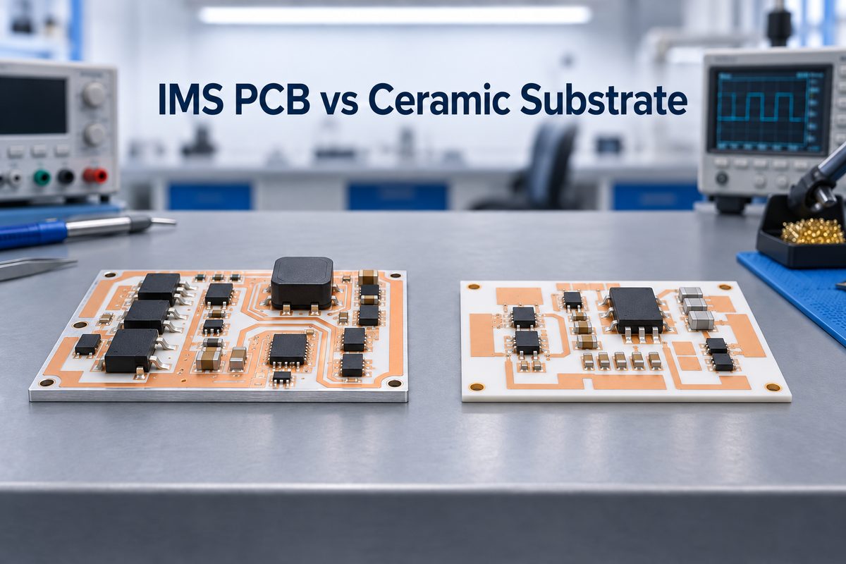
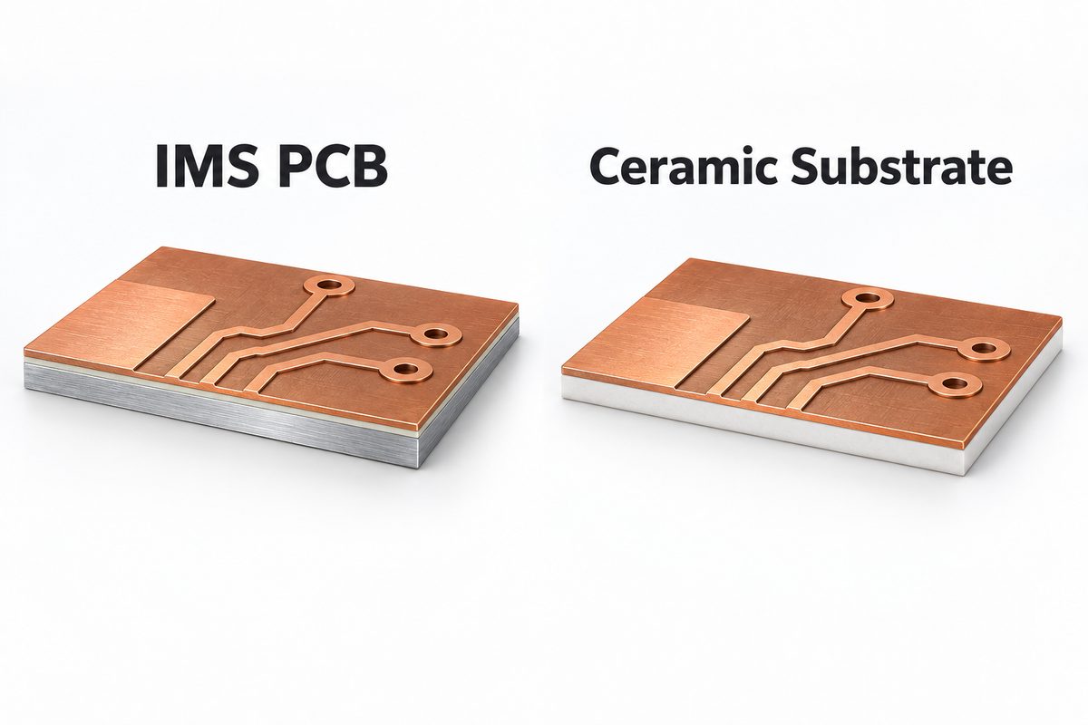
copper core PCB supplier
A copper-core PCB integrated with a heat spreader for power electronics.

How Is Copper Base PCB Quality Controlled Before Shipment?

Copper base PCB quality control should result in fewer insulation, dimensional, soldering and mechanical-fit problems after delivery.

At EBest Circuit, attention is focused on the areas that directly affect the finished board:

  • Construction consistency: copper thickness, dielectric structure and finished thickness follow the approved specification.
  • Electrical isolation: insulated structures must maintain separation between the circuit and metal substrate.
  • Hole accuracy: standard PTH diameter tolerance is ±0.075 mm, while NPTH tolerance can reach ±0.05 mm.
  • Mechanical fit: standard outline tolerance is ±0.15 mm, with ±0.10 mm available for qualifying requirements.
  • Solderability: pads, solder mask and surface finish are checked before assembly.
  • Electrical integrity: electrical testing helps detect opens and shorts before shipment.

When the copper core PCB continues into assembly, inspection can extend to SPI, AOI, X-ray, ICT and functional testing according to the board and acceptance requirements.

The benefit is not simply more inspection steps. It is less risk of discovering a PCB problem after higher-value components have already been mounted.

copper core PCB supplier
Dimensional inspection of a copper-core PCB before assembly.

Which Certifications and Standards Matter for Copper Core PCB Production?

Not every copper core PCB needs the same certification set. The relevant requirements depend mainly on the final product and the customer’s supplier-qualification rules.

Application Common Requirement
IndustrialISO 9001, IPC
AutomotiveIATF 16949
MedicalISO 13485
AerospaceAS9100D
EnvironmentalRoHS, REACH
UL-required productsApplicable UL system

EBest Circuit supports projects under quality systems including ISO 9001, ISO 13485, IATF 16949 and AS9100D, together with applicable UL, RoHS, REACH and IPC requirements.

The important point is not to require every certificate for every board.

An automotive copper-base PCB may make IATF 16949 part of supplier qualification. A medical project may require ISO 13485, while an aerospace program may use AS9100D as a sourcing gate.

For a general industrial copper core PCB, the applicable IPC requirements, materials and customer acceptance criteria may matter more than an unnecessarily long certification list.

The right certification should qualify the manufacturing route, not simply decorate the supplier page.

How Fast Can Copper Core PCB Prototypes and Production Orders Ship?

For standard PCB builds, EBest Circuit typically plans around 3–5 working days, with expedited production available for qualifying projects.

Copper core PCB lead time may increase when the design includes:

  • high-conductivity material requiring special sourcing;
  • non-standard copper-base thickness;
  • multilayer construction;
  • thermoelectric-separation structures;
  • special machining;
  • additional testing.

For the customer, the real benefit is knowing the realistic ship date before production starts.

We consider engineering review, material readiness, fabrication, assembly and testing when estimating the schedule. A three-day fabrication cycle, for example, has little value if the specified 5 W/m·K material requires additional sourcing time.

For PCBA orders, component availability must also be included before a dependable delivery date can be confirmed.

Can a Copper Core PCB Supplier Also Handle PCBA?

Yes. For many thermal-management products, having one supplier handle both copper core PCB fabrication and assembly can simplify the project considerably.

A copper-base board may later carry LEDs, MOSFETs, power modules, connectors or other heat-generating components. Splitting these stages can leave the customer coordinating:

PCB supplier → component sourcing → SMT house → inspection → testing

EBest Circuit can combine these activities within one manufacturing project.

Customers gain:

  • Fewer supplier handoffs: PCB, sourcing, assembly and testing can stay together.
  • Faster issue resolution: PCB and assembly questions are handled within the same project.
  • Better BOM control: turnkey, partial-turnkey and consigned sourcing are available.
  • Inspection matched to the build: SPI, AOI and X-ray can be applied where appropriate.
  • Clearer responsibility: PCB-related assembly issues do not need to be negotiated between separate factories.

This approach is particularly useful for LED lighting, power electronics, industrial control and automotive applications where the PCB and mounted devices work together as one thermal system.

copper core PCB supplier
Thermal inspection of an assembled copper-core PCB with its metal core visible.

Copper Core PCB Case Study: From Thermal Design to Production

One copper-core lighting project required a 2-layer copper core PCB with downstream assembly.

Item Specification
PCB2-layer copper core
Thickness1.60 mm ±10%
Circuit copper1 oz
Thermal conductivity3 W/m·K
FinishOSP
AssemblyIncluded
ApplicationPool lighting

The customer needed more than a bare copper-base board. The 3 W/m·K thermal material, 1.6 mm construction, surface finish and assembly process had to work within the same finished lighting product.

EBest Circuit coordinated PCB fabrication and PCBA within one project rather than transferring the board between separate manufacturers.

For the customer, this meant fewer supplier interfaces and one approved manufacturing package that could support repeat builds.

The project also shows why a copper core PCB should not be specified simply as “use copper.” Thermal dielectric, copper weight, board thickness, surface finish and downstream assembly all affect the finished product.

Why Choose EBest Circuit as Your Copper Core PCB Supplier?

A good copper core PCB supplier should reduce the work and risk the customer has to manage.

With EBest Circuit, buyers gain:

  • More design flexibility: standard and special copper-base structures can be evaluated against clearly defined process limits.
  • One manufacturing route: PCB fabrication, sourcing, PCBA and testing can stay within one project.
  • Fewer surprises before fabrication: thermal material, copper weight, thickness and assembly requirements are reviewed before release.
  • Better control over changes: material and component alternatives remain subject to customer approval.
  • Easier repeat production: approved construction and production requirements remain connected to future orders.
  • Broader quality-system coverage: industrial, automotive, medical and aerospace projects can be supported under relevant quality frameworks.

For international customers, the value is not simply a lower bare-board price. It is knowing what the factory can manufacture, reducing supplier handoffs and keeping responsibility clearer from copper-core PCB fabrication through finished PCBA.

FAQs About Copper Core PCB Suppliers

How do I choose a copper core PCB supplier?

Start with measurable manufacturing limits. Compare the required thermal conductivity, copper weight, board thickness, layer structure, minimum hole, trace/space, surface finish and quality requirements with the supplier’s actual production capability.

Is copper core PCB better than aluminum PCB?

Not in every application. Copper provides stronger heat spreading and can suit more demanding thermal designs, but it is heavier and usually more expensive. Aluminum remains practical for many LED and power-electronics applications where its thermal performance is sufficient.

What thermal conductivity should I specify for a copper core PCB?

Do not judge the PCB by bulk copper conductivity alone. The thermal dielectric and its thickness can strongly affect overall thermal resistance. EBest Circuit regularly supports 1W, 2W and 3W thermal materials, while 3–8 W/m·K materials can be evaluated according to availability and construction.

How thick can a copper core PCB be?

EBest Circuit’s regular metal-base PCB thickness range is 0.8–3.0 mm. Thicknesses of 4.0 mm or 5.0 mm can be evaluated when suitable material is available.

Can copper core PCBs use heavy circuit copper?

Yes. Regular inner-layer copper capability is 0.5–3 oz, while outer layers commonly support 1–3 oz. Higher copper weights require review because trace/space and etching requirements change as copper becomes thicker.

Can one copper core PCB supplier provide both fabrication and assembly?

Yes. EBest Circuit provides copper core PCB fabrication together with component sourcing, SMT/THT assembly, inspection and customer-defined testing, reducing the need to coordinate several manufacturing suppliers.

Ready to Start Your Copper Core PCB Project?

If you are preparing a copper core PCB or PCBA project, send your Gerber files, fabrication drawing, BOM, assembly requirements, and target quantity to sales@bestpcbs.com. Our engineering team can review the stackup, copper-base structure, thermal requirements, manufacturability, assembly needs, and lead time before quotation.

You may also like

Industrial Control PCB Manufacturer Australia: 10 Companies to Compare

September 8th, 2026

Finding the right industrial control PCB manufacturer Australia buyers can rely on is not simply a matter of choosing the nearest factory or the lowest unit price. A control board may operate pumps, motors, relays, sensors, safety circuits, or communication modules for years in an electrical cabinet. One weak solder joint, unsuitable laminate choice, undocumented component substitution, or incomplete functional test can stop the equipment that depends on it.

Australian OEMs therefore need to compare manufacturers by project fit: bare-board capability, component sourcing, assembly, inspection, testing, traceability, engineering response, and repeat-order control. EBest Circuit (Best Technology) supports this complete path through its own PCB and PCBA factories, a supply network of more than 1,000 partners, 20 years of PCBA experience, and quality systems including ISO 9001, ISO 13485, IATF 16949, and AS9100D. To discuss an industrial control PCB or PCBA requirement, contact sales@bestpcbs.com.

industrial control PCB manufacturer Australia
Industrial control PCBA inspection for an Australian OEM manufacturing project.

Industrial Control PCB Manufacturer Australia: 10 Companies to Compare in 2026

The following manufacturers represent different sourcing models available to Australian industrial-control buyers, including local PCB fabrication, contract electronics manufacturing, and Australian-managed supply routes.

  1. Alfatron – A Victoria-based manufacturer offering onshore PCB fabrication and assembly. Its published services include prototype assembly, AOI, ICT, X-ray inspection, conformal coating, and electromechanical assembly. It is a relevant candidate when sovereign Australian production is a firm requirement.
  2. Circuitwise Electronics Manufacturing – A Sydney-based contract electronics manufacturer serving high-reliability industrial and regulated applications. Its published scope includes SMT and through-hole assembly, FAI, 3D AOI, X-ray, box build, functional testing, and component-level traceability.
  3. Precision Electronic Technologies – An Australian engineering and manufacturing provider supporting PCB development, sourcing, assembly, and production. Its manufacturing network can suit buyers comparing local engineering access with a broader supply footprint.
  4. Elemental Electronics – A Victorian electronics developer and manufacturer focused on prototype and low-to-medium-volume production. It provides PCB assembly, product integration, test-fixture development, functional testing, and enclosure work.
  5. Hetech – A Brisbane electronics manufacturing provider offering prototyping, PCB assembly, inspection, testing, coating, and product integration. Its published industry coverage includes industrial automation and other high-reliability applications.
  6. Advanced Technology and Manufacturing (AT&M) – A Perth-based assembly provider supporting low- and higher-volume PCBA. Its published production capabilities include SMT, through-hole assembly, reflow, wave soldering, and workmanship aligned with IPC/J-STD requirements.
  7. OurPCB Australia – A PCB and PCBA supplier serving Australian customers through an overseas manufacturing model. It may fit buyers who want local communication while sourcing boards or assemblies from Asia.
  8. Rush PCB Australia – A supplier covering PCB prototypes, fabrication, and assembly for the Australian market. Buyers should confirm the production location, applicable capabilities, quality records, and test scope for their exact control-board build.
  9. QualiEco Circuits – An Australian supplier of PCB fabrication and contract assembly services. It can be considered for prototype, urgent, and repeat-order needs where an Asia-linked supply route is acceptable.
  10. Crystalaid – An Australian-owned and operated electronics manufacturer based in Queensland. Its published capabilities include SMT and through-hole PCB assembly, cable and harness assembly, testing, and box build for industrial and other high-reliability applications.

Shortlisting tip: Choose three or four candidates whose production model matches the project. Send each supplier the same controlled RFQ package and compare the resulting assumptions, exclusions, technical questions, test plan, evidence package, and delivery commitment – not only the quoted price.

Australia-Based vs China Industrial Control PCB Manufacturers

The better manufacturing location depends on what the project must protect. A local Australian supplier may be attractive when face-to-face engineering access, sovereign production, small local runs, or regulated procurement rules are decisive. A qualified China-based supplier can be competitive when the buyer needs a broader PCB process range, coordinated component sourcing, scalable assembly capacity, or cost control across repeat orders.

Decision Australia-based supplier China-based supplier
CommunicationLocal time zone and easier site accessConfirm response owner and engineering handoff
ProductionUseful when onshore manufacture is mandatoryBroader capacity and supply-chain options may be available
CostCan suit low-volume or locally controlled workOften competitive for integrated and repeat production
LogisticsShort domestic transport routeRequires freight, customs, and buffer planning

The country alone does not determine risk. Before nomination, compare revision control, approved-vendor handling, first-article approval, nonconformance response, test ownership, traceability, and the supplier’s ability to reproduce the same build months later.

Australian buyers can also use a hybrid sourcing strategy. Early engineering builds or sensitive programs may stay local, while a qualified China partner supports cost-controlled repeat production. The key is to release the same approved files, BOM, test limits, and change-control rules to every manufacturing route.

Industrial Control PCB Capabilities for Australian Automation Projects

EBest Circuit manufactures FR-4, heavy-copper, rigid-flex, metal-core, and ceramic boards for industrial controllers, power interfaces, motor-control units, and monitoring equipment.

Industrial-control requirement EBest Circuit capability
FR-4 layers and materials1–10 layers standard
Up to 32 layers after review
Low-, mid-, and high-Tg FR-4
Copper and geometryCopper up to 5 oz
4/4 mil line and space
0.20 mm finished holes
Special processesHeavy copper up to 20 oz
3/3 mil line and space
0.15 mm finished holes after review
Thickness and finishCommon thickness: 0.4–3.5 mm
HASL, OSP, ENIG, immersion silver/tin, ENEPIG, and hard gold
Other board typesRigid-flex: up to 20 layers
MCPCB: up to 10 layers
Thin-film, DBC, DPC, and AMB ceramic boards
industrial control PCB manufacturer Australia
Dimensional inspection of multilayer industrial control PCBs before assembly.

Special-process limits require project review. Send the Gerbers, drill files, fabrication drawing, stack-up, impedance requirements, IPC class, and critical tolerances. EBest Circuit can then confirm the production route and return DFM questions before release.
Industrial Control PCB Assembly for Australian Orders

EBest Circuit provides SMT, through-hole, and mixed-technology assembly for Australian industrial-control orders. This is useful for boards that combine fine-pitch ICs with relays, terminal blocks, transformers, large connectors, heat sinks, or other through-hole components.

PCBA item EBest Circuit capability
Placement capacityCompany capability data lists up to 13,200,000 component placements per day
Board sizeFrom 0.2 × 0.2 inches to 20 × 20 inches; boards up to 22 × 47.5 inches require project review
Small componentsDown to 01005 packages
Fine-pitch packagesBGA pitch down to 0.25 mm
Assembly processesSMT, THT, and mixed assembly
Component packagingReels, cut tape, tubes, trays, and loose parts
Assembly production timeCapability data lists 1–5 days, subject to BOM readiness, process complexity, inspection, and testing
industrial control PCB manufacturer Australia
Mixed-technology industrial control PCB assemblies moving through production.

EBest Circuit can manage turnkey, consigned, or partial-turnkey builds. The service can combine BOM review, approved component procurement, stencil preparation, solder-paste printing, placement, reflow, through-hole insertion, wave or manual soldering, programming, cleaning, coating, testing, and final packaging according to the released order scope.

Before purchasing components, the team reviews manufacturer names, part numbers, packages, quantities, lifecycle risks, and approved-substitution rules. When a part is obsolete or has an unsuitable lead time, EBest Circuit can prepare a BOM optimisation or alternative-parts list for customer approval. No substitute is released merely because stock is available.

To receive a complete PCBA quotation, provide the BOM, centroid data, assembly drawings, Gerbers, approved-vendor requirements, soldering standard, programming files, test procedure, first-article quantity, production quantity, and repeat-order forecast.

Testing Evidence for Industrial Control PCB Orders to Australia

EBest Circuit can provide a project-specific inspection and test evidence package for Australian industrial-control orders. The exact records are agreed before production so that the delivered documentation matches the customer’s acceptance plan.

Available production and quality evidence includes:

  1. incoming-material and component verification records;
  2. solder-paste inspection records when SPI is included in the process plan;
  3. AOI results covering component position, polarity, solder condition, and missing parts;
  4. X-ray images or records for BGA, QFN, and other bottom-terminated packages when required;
  5. bare-PCB open-and-short electrical-test results;
  6. ICT or flying-probe results where the board design and agreed test route permit them;
  7. programming confirmation and functional-test results measured against customer-approved limits;
  8. first-article inspection and approved-deviation records; and
  9. final inspection, serial-number, batch, material, and process-traceability records.
industrial control PCB manufacturer Australia
Functional and electrical verification of an industrial control PCBA.

EBest Circuit’s digital workshop records material and product batches, production stages, and manufacturing progress. This helps the team retrieve the corresponding production information quickly when a customer reviews a batch, repeat order, or quality issue.

For functional testing, the customer should provide the procedure, firmware version, expected inputs and outputs, pass/fail limits, connector pinout, fixture interface, golden sample, and any required load or communication simulator. EBest Circuit can then implement the approved test at PCBA level and return the agreed results with the shipment.

Quality Certifications for Industrial Control PCB Manufacturing in Australia

A certificate is useful only when its scope and controls match the project. Buyers should request the current certificate, issuing body, covered site, expiry date, and manufacturing scope rather than relying on a logo displayed on a website.

Match the evidence to the application:

  • ISO 9001 supports a general quality-management framework.
  • ISO 13485 may be relevant when the control assembly forms part of a medical-device supply chain.
  • IATF 16949 is relevant to automotive production controls when the project and manufacturing site fall within scope.
  • AS9100D supports aerospace and defence quality-system requirements when applicable.
  • IPC-A-600, IPC-A-610, IPC/WHMA-A-620, and J-STD-001 can define board, assembly, cable, and workmanship expectations when specified in the purchase package.

Beyond certificates, audit how the manufacturer controls incoming material, shelf life, calibration, ESD, nonconforming product, rework, corrective action, approved suppliers, engineering changes, and production records. The purchase order should state the required IPC class and any customer-specific acceptance criteria.

Lead Times for Industrial Control PCB Prototypes and Repeat Orders to Australia

EBest Circuit offers normal and expedited production for industrial-control prototypes. The published FR-4 times below apply to standard-specification prototype orders below one square metre. The PCBA figures cover assembly production and still depend on component readiness, fixture requirements, programming, coating, and the approved inspection plan.

Product Normal service Fastest service
1-layer FR-4 prototype7 days24 hours
2-layer FR-4 prototype8 days24 hours
4-layer FR-4 prototype10 days48 hours
6-layer FR-4 prototype10 days72 hours
8-layer FR-4 prototype12 days72 hours
PCBA1 week2 days

The standard FR-4 reference covers normal FR-4 material from 0.4–1.6 mm, 0.5 or 1 oz copper, lead-free HASL, green solder mask, white silkscreen, line width and spacing above 8 mil, minimum hole above 0.3 mm, and minimum annular ring above 10 mil. A control board with heavy copper, fine lines, controlled impedance, special laminate, blind vias, coating, or unusual testing needs a project-specific schedule.

For an Australian shipment, EBest Circuit confirms the manufacturing schedule after reviewing PCB complexity, BOM availability, first-article approval, testing, documentation, and freight requirements. Repeat orders can move faster when the approved Gerbers, BOM revision, placement program, stencil, fixture, test limits, golden sample, and deviations remain under the same controlled revision.

Why Australian OEMs Choose EBest Circuit for Industrial Control PCB Projects

EBest Circuit supports Australian buyers who want one accountable manufacturing path from bare PCB through tested assembly. The business value is strongest when the project involves several technical handoffs that would otherwise be divided among unrelated suppliers.

Project support can include:

  • in-house PCB and PCBA production coordinated under one order;
  • DFM pre-review and a BOM optimisation list before release;
  • PCB, component, assembly, and testing engineers supporting the customer’s commercial contact;
  • prototype and small-batch builds for engineering validation before repeat production;
  • sourcing support through more than 1,000 supply-chain partners;
  • ISO 9001, ISO 13485, IATF 16949, and AS9100D quality systems, subject to project applicability; and
  • digital batch and material tracking designed to retrieve production information within seconds.

The company has 20 years of PCBA experience and reports service to more than 10,000 engineers and 1,800 customers. Australian buyers may also arrange a factory visit to review the PCB and PCBA lines, inspection equipment, traceability controls, and the proposed production route before supplier approval.

Send sales@bestpcbs.com your controlled files, target quantity, application, testing requirements, and requested delivery date. The engineering team can then return project-specific questions and a quotation instead of a price based on incomplete assumptions.

Case Study: Industrial Control PCB for an Australian Automation System

An Australian customer ordered a 600-piece batch of four-layer FR-4 control boards for a battery-powered equipment system. The released specification called for a finished thickness of 1.6 mm, Tg of at least 170 degrees C, 35-micrometre internal and base outer-layer copper, ENIG with 3 microinches of gold, UL 94V-0 material, and RoHS-compliant production.

The board also carried manufacturing requirements that directly affected supplier selection:

  • minimum plated-through-hole copper of 20 micrometres;
  • minimum annular ring of 0.15 mm;
  • solder-mask registration tolerance of +/-0.10 mm;
  • automatic open-and-short electrical testing at 250 V;
  • AOI and X-ray inspection after assembly;
  • board cleaning after SMT with defined cosmetic acceptance requirements; and
  • COC, electrical-test, copper-thickness, and final inspection reports.

EBest Circuit reviewed the fabrication package and assembly requirements before production, confirmed the panelisation and test expectations, and coordinated PCB fabrication with the following SMT build. One additional sample accompanied the 600 production boards for approval and quality reference.

This project shows why an industrial-control buyer should include measurable acceptance criteria in the RFQ. Board material, copper, plating, solder-mask tolerance, electrical-test voltage, cleaning, inspection method, and required reports were defined before manufacturing rather than left to general factory practice.

For a comparable Australian control-board project, send the Gerber files, fabrication drawing, BOM, placement data, assembly drawing, test limits, inspection requirements, production quantity, sample requirement, and delivery target to sales@bestpcbs.com. EBest Circuit can review the complete package and identify any manufacturing or documentation question before quotation and production release.

FAQs About Industrial Control PCB Manufacturer Australia

1. Should an Australian industrial-control OEM choose a local or overseas PCB manufacturer?

Choose according to the project’s procurement rules, engineering access, production volume, process requirements, cost target, and supply-chain risk. Local manufacture may be important for sovereign or highly sensitive work. A qualified overseas partner may be suitable when broader PCB capability, integrated sourcing, assembly capacity, or repeat-production cost is more important.

2. What files are required for an accurate industrial control PCB quotation?

Send Gerber and drill files, fabrication drawing, stack-up and impedance requirements, BOM, centroid data, assembly drawings, approved-substitute rules, firmware, test procedure, acceptance limits, quantity, and delivery target. Add enclosure or cable information if mechanical assembly is included.

3. Which tests should be specified for an industrial control PCB assembly?

The plan may combine bare-board electrical test, solder-paste inspection, AOI, X-ray, in-circuit testing, programming, and functional testing. Select methods according to component packages, circuit access, safety risk, expected failures, production volume, and the functions that must be verified before shipment.

4. Can EBest Circuit support prototypes and repeat industrial-control production?

Yes. EBest Circuit supports prototypes and small batches for design validation, then repeat PCBA production using the approved files, BOM, process settings, inspection requirements, and test limits. Lead time remains dependent on board complexity, component availability, fixture readiness, and production loading.

5. How should buyers audit an industrial control PCB manufacturer serving Australia?

Review the applicable certificates, factory scope, process capability, approved-supplier controls, ESD and calibration systems, material traceability, inspection equipment, test records, change control, nonconformance handling, and repeat-order controls. To evaluate EBest Circuit for an industrial control PCB manufacturer Australia project, arrange a factory visit or send the controlled RFQ package to sales@bestpcbs.com.

You may also like