For a first-pass PCB power integrity check, divide the allowed transient voltage change at the load by the estimated change in load current. The result is a starting target for the impedance of the power delivery network (PDN). Apply it over a relevant frequency range and verify the actual voltage waveform. A single target value cannot tell you whether the regulator, the board or the package causes a failure.
Consider a hypothetical processor rail that droops when a block starts working. Follow that one rail from its voltage specification to a defensible test, rather than adding capacitors until one waveform looks better.
Define the Power Path From Regulator to Load
Draw the supply and return together. The network includes the voltage regulator, board copper, vias and capacitors between the source and the processor; the package and on-die behavior can matter at higher frequencies. Define which parts your model includes and where the device specification expects voltage to be checked.
Set Aside Only the Voltage Available for the Step
Start from the device’s voltage limits and reserve room for applicable setpoint error, DC drop and ripple before assigning a dynamic budget. The amount left is not necessarily symmetric for a load increase and a load release. Document the accounting so no one spends the same margin twice.
Work Out the Target Impedance in Milliohms
Use the current change, not the rail’s maximum DC current. These illustrative inputs are not a device specification or a recommended PCB limit.
| Input | Example | Use |
| Nominal rail | 1.0 V | Identifies the modeled rail |
| Dynamic allowance | 30 mV | Available for the modeled transient |
| Current increase | 2 A | Change during the event |
| First-pass target | 15 mΩ | 0.030 V divided by 2 A |
Keysight’s PDN application note explains why the effective impedance of a processor power network needs to be considered across frequency. The example above is an illustration of the budgeting method, not a published device limit.
Choose the Frequency Range From the Actual Event
A fast current edge contains higher-frequency content than a slow edge. Long events also depend on lower-frequency regulator behavior. Use the device and regulator guidance, relevant current waveforms, and model boundaries to select the band. A flat starting target is not a universal mask extending to unlimited frequency.
Compare DC Drop, Impedance and Transient Checks
These checks answer different questions. Run the ones that cover your design risks rather than expecting any one result to certify the rail.
| Check | Answers | Does not show alone |
| DC voltage drop | Loss under steady load | Ringing after a step |
| Impedance sweep | Weak frequency bands at a port | Exact droop for a real event |
| Load-step waveform | Droop and recovery for the applied event | All untested waveforms and conditions |
Model the Capacitors as Installed
Use capacitance at the operating bias and include the model’s resistance and inductance. Add the mounting loop formed by pads, vias and reference planes where the model requires it. A capacitor that looks effective in isolation may contribute little at the load if the connection adds too much inductance.
Check Where the Current Returns
Review the power and ground path as a loop. A nearby capacitor does not help as expected if its return reaches the processor through a long or narrow route. Use the manufactured stackup and actual via locations, then compare the revised model at the same observation port.
Investigate Peaks Before Adding Another Value
A peak can result from interactions between inductive and capacitive paths. Adding a different capacitor value can shift a peak rather than remove it. Compare the response before and after one controlled model change; preserve regulator stability and verify any actual part change against the regulator documentation.
Observe the Rail at the Load
Plan a measurement point and return that represent the device-side voltage as closely as the board allows. Record probe method, bandwidth and where the load step is applied. If you measure at the regulator and the load, do not assume a clean regulator waveform proves a clean processor rail.
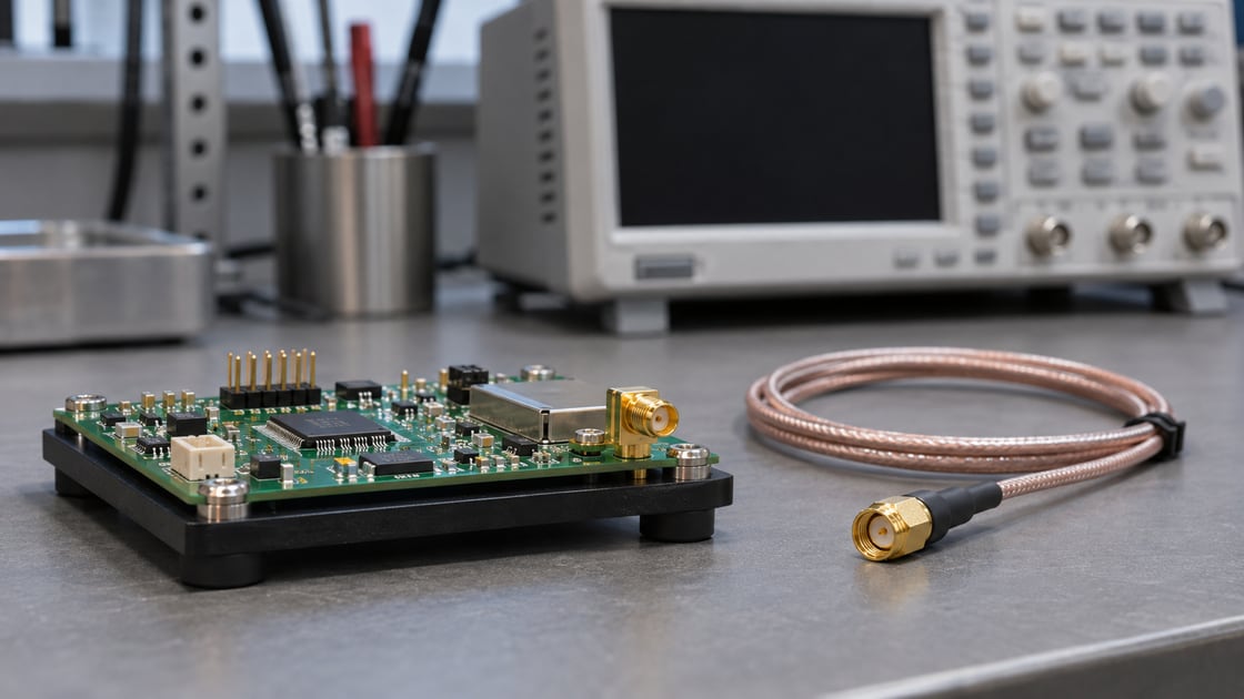
Correlate the Sweep With the Time-Domain Waveform
Use the sweep to locate a candidate weak band and the waveform to test its impact under the actual event. Compare port locations and operating conditions before linking a ring frequency to an impedance peak. A mismatch can be a clue about the fixture, the model or a different source of noise.
Change the Part of the Network That Fails
If a long droop dominates, investigate regulator response and bulk delivery. If a fast local dip dominates, start with local decoupling and its connection. If a narrow ringing band dominates, evaluate resonance and damping. These are diagnostic starting points, not automatic fixes; verify against the same event and observation point.
Release the Rail With a Reproducible Test
Keep the voltage budget, current-step assumptions, stackup, simulation ports, and measurement method with the board revision. Define pass limits from the device and system requirements. For the broader design workflow, see the Best Technology PCB power integrity guide.
FAQ
Is target impedance the same as 50-ohm trace impedance?
No. A signal line’s characteristic impedance describes wave propagation along an interconnect. The PDN target is a limit or goal for the effective impedance seen at a defined power port. They solve different problems and have different measurement and modeling requirements.
Can I use the processor’s rated maximum current as the step?
Only if it represents the defined load change from the starting operating point. A current rating describes a limit or condition, not automatically the waveform the PDN must support. Ask for an applicable load profile or document the conservative assumption and validate it with a relevant test.
Does the same target apply at both ends of the board?
Not necessarily. Impedance depends on the measurement port and its return. A reading at the regulator and a reading near the processor can differ because copper and vias lie between them. Specify the port in both the model and the test before comparing results.
Should a powered rail be connected directly to a VNA?
Do not make that connection without a qualified measurement setup. Instrument input limits, DC isolation, calibration, grounding and the rail’s operating state all matter. Start with the instrument manufacturer’s method, such as Keysight’s low-impedance measurement note, and the lab’s approved protection plan. A connection intended for an unpowered board may not be safe on a powered rail.
Why is the oscilloscope result sensitive to probe ground?
A long ground connection can add loop inductance and pick up nearby fields, making a fast edge look worse or different. Compare the waveform using the approved short-return or equivalent fixture and record the setup. Treat a change caused by the measurement connection as a measurement issue first.
Will more capacitance always improve the waveform?
No. Extra capacitance can help in one frequency range while changing resonances or regulator behavior elsewhere. Start with a specific failure signature, make one justified change, and compare results under the same conditions. Check start-up and regulator requirements as well as the load-step waveform.
Does a passing impedance sweep eliminate the need for a load step?
No. The sweep is defined by its port, frequency band and operating conditions. It does not apply the product’s actual workload or capture every nonlinear regulator response. Use a controlled time-domain test to check the voltage excursion and recovery for the relevant operating event.
Can I reuse the target for another board with the same processor?
Only after checking the rail, operating modes, current event, budget and reference point. A new stackup, regulator, package option or workload can change the design and validation requirements. Carry forward the documented assumptions, not just the final number, so the next review can identify what changed.
Request a Layout Review
Send the stackup, rail layout, load-step assumptions and measurement locations to sales@bestpcbs.com when requesting a PCB review.