PCB manufacturing PCB manufacturing
Home > Blog

copper resistance

PCB Trace Neck-Down: Where High-Current Routes Get Hot
Friday, November 6th, 2026

A wide copper pour does not protect a power route if the current must squeeze through a narrow connection at its end. Calculate the neck separately from the rest of the path, then verify temperature on the assembled board. Resistance can be estimated from geometry; temperature also depends on how heat escapes.

What Counts as a Neck-Down?

A neck-down is a local reduction in conductor cross-section. It can occur at a connector pad, fuse land, layer transition, clearance cutout or thermal relief. Follow the actual current path rather than looking only at the largest visible pour.
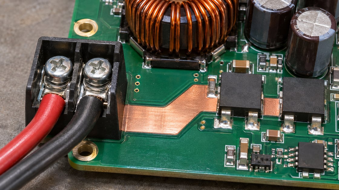
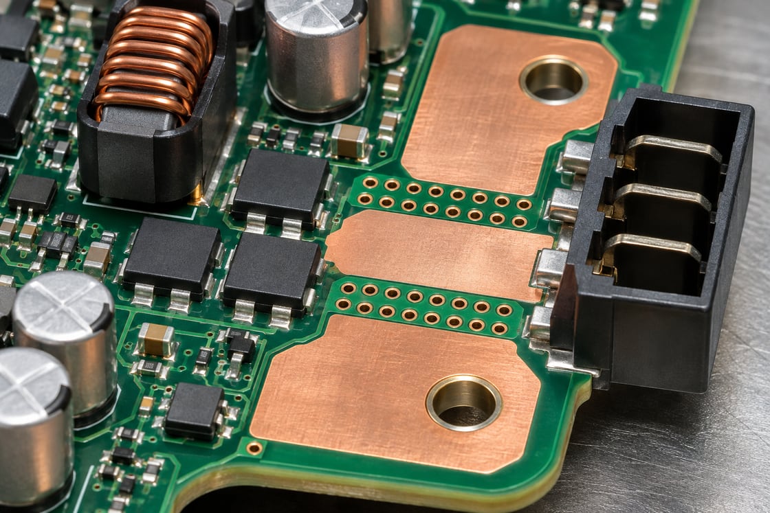
Power PCB and terminal near a local copper transition
AI-generated illustration of a power-board layout, not a verified hotspot.

Why the Short Segment Deserves Its Own Calculation

Series segments carry the same steady current, but their resistance per unit length can differ. Texas Instruments’ copper-trace shunt note explains geometry-dependent resistance and the influence of copper temperature. A power connection is not necessarily designed to act as a shunt.

Detailed Inputs for the Resistance Estimate

Parameter Example Purpose
— — —
Steady current 12 A Voltage and loss estimate
Neck length 2.0 mm Defines the segment
Finished neck width 0.60 mm Sets the cross-section
Finished copper thickness 70 µm Sets the cross-section
Copper resistivity 0.0172 Ω·mm²/m Approximate room-temperature input

Narrow Segment vs Wide Pour

Section Example width Approximate resistance per mm
— — —
Neck 0.60 mm 0.410 mΩ
Main route 3.00 mm 0.082 mΩ
Ratio at equal thickness Five to one in width Five to one in resistance per length

Worked Example: Two Millimetres at Twelve Amps

For a rectangular section, R = resistivity × length ÷ area. The neck area is 0.042 mm² and its resistance is about 0.82 mΩ. At 12 A that is about 9.8 mV and 0.118 W. These are hypothetical values before allowing for temperature, contact or current spreading.

Compare the Neck With the Whole Path

A 10 mm length of the 3 mm route has approximately the same ideal resistance as the 2 mm neck. The losses are similar, but one is generated in a much shorter region. Do not infer the same temperature rise; nearby copper, pads and the enclosure can change heat spreading.

Do Not Use Artwork Width as the Only Input

Ask for the relevant finished copper geometry and confirm the narrow section after all clearances and pattern changes. The rectangular approximation becomes less representative where conductor sidewalls slope or the current spreads into a pad.

Compare Widening With a Parallel Route

Widening the neck is straightforward if spacing and soldering constraints allow it. Adding a parallel path can help, but a route that rejoins through the same constriction has not removed it. Verify connection points, vias and current distribution before counting the new copper.

Keep Connector and Joint Heating Separate

A hot terminal can involve the PCB copper, solder joint, contact or wire termination. Measure voltage across the suspected board segment separately where practical. Do not attribute total voltage drop across an assembled connector to the etched trace alone.

Test the Actual Operating Condition

Use the relevant load, enclosure, airflow and ambient condition. Record duration and the temperature measurement method. With infrared equipment, account for surface emissivity rather than comparing bare shiny copper and dark solder mask without a suitable method.
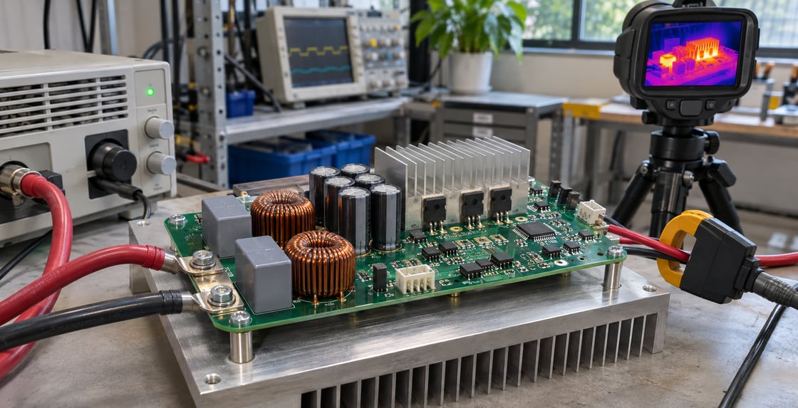
Power PCB on a test bench with thermal inspection equipment
AI-generated illustration of testing context, not a measurement.

Check Pulse and Continuous Duty Separately

A short pulse and steady load can create different temperature histories. Calculate electrical loss for the applicable current waveform and verify the thermal response when it matters. Do not apply an illustrative steady-current result as a pulse rating or protection setting.

Carry the Bottleneck Into the Release Review

Mark the narrow section, its finished geometry and the intended verification. The BestPCBs high-current PCB guide covers the wider power-board design. Keep the local calculation linked to the specific pad, connector and drawing revision.

Request a Power Layout Review

Send the current profile and marked bottleneck to Best Technology.

FAQ

Is a two-millimetre neck too short to matter?

Not necessarily. Its importance depends on cross-section, current and the surrounding heat path. Estimate the voltage drop and loss for that segment separately, and compare it with the longer route. If the design is thermally sensitive, check the assembled board under representative conditions.

Can I turn watts directly into temperature rise?

Not without a suitable thermal model or measured relationship for that structure. The same loss can produce different temperatures depending on heat spreading, airflow and nearby materials. Treat electrical power as an input to the thermal problem, not as the final temperature.

Does heavier copper solve every neck-down?

No. Greater thickness may reduce resistance, but it does not remove connector limitations, contact loss, or restrictions from spacing and the fabrication process. Check the finished geometry and follow the current through the pad and any layer transitions before accepting the wider design.

Is a copper pour always better than a trace?

A pour can be useful, but its effective connection can still be limited by a narrow gap, pad entrance or thermal relief. Examine the whole route including the connection points. The largest area of copper is not necessarily the section that determines local loss.

Can I measure the neck resistance with a multimeter?

Very low resistance may be hard to distinguish from lead and contact resistance using an ordinary two-lead setup. Use an appropriate four-terminal measurement or measure voltage drop at a known current where practical. Define the probe points so the result does not include unrelated joints.

Why is the connector hotter than the calculation suggests?

The calculation may describe only the etched copper, while the actual temperature includes heating from the terminal, solder joint or contact resistance. Check the voltage drop of each accessible segment and compare under controlled conditions rather than assigning all the heat to one component.

Should I remove every thermal relief on a power pad?

Not automatically. A solid connection can reduce constriction but can also change assembly heating and solderability. Review the electrical requirement and the assembly process together. If a relief is retained, check the total effective connection and verify the final design under load.

What if two parallel paths have different lengths?

Different lengths and cross-sections can create different resistances, so current need not divide equally. Check the connections, via paths and operating temperature as well as nominal width. Verify each branch if unequal sharing could create a hot spot or exceed a local limit.

You may also like

Parallel PCB Power Vias: Why Current Does Not Split Evenly
Friday, November 6th, 2026

Parallel PCB power vias share current evenly only when their effective paths are sufficiently similar. A via near the incoming trace can carry more current than one behind a narrow copper neck. A single-via calculator can estimate the barrel, but it cannot see those paths or establish the temperature of the array.

Follow a hypothetical DC power converter board where 4 A must transfer from a top copper pour to a bottom pour. Two paths make the math visible; the same questions apply to larger arrays.

Follow the Current Beyond the Via Barrel

Draw the path from the upstream copper to each via, down the plated wall and through the downstream copper. That complete path sets the division in a simple resistive model. If the copper is shared between branches, model the shared section separately rather than counting it twice.

Populated power board with a plated via array
AI-generated illustration of power-board context; not a verified current path or layout recommendation.

Compare an Ideal Array With a Constricted Layout

Use equal sharing as a starting assumption only when the geometry supports it. This table compares situations for the same current transfer.

Layout First assumption Check next
Symmetric feed and exit Similar branch paths Confirm both sides and barrel geometry
Narrow feed at one end Closest path may dominate Inspect the constriction and current density
Common copper bottleneck All current crosses the neck Check the neck separately from the vias

Record Barrel and Access Parameters Separately

Use finished dimensions from the manufacturer, not the nominal drill alone. The barrel resistance depends on the length of the conducting path and the copper cross-section, not just hole diameter. The worked example uses assumed branch resistances to isolate the effect of access copper.

Parameter Unit Needed for
Finished hole diameter mm Barrel geometry
Wall plating thickness µm Copper cross-section
Conducting barrel length mm Resistive path between used layers
Access resistance mΩ per branch Copper on both sides of the barrel
Load and thermal conditions A, duty cycle, ambient Validation under the actual duty

Calculate Current for Two Unequal Branches

Take two independent parallel paths between common nodes. Each barrel is assumed to be 1 mΩ. Path A has another 1 mΩ of access resistance, and B another 3 mΩ, giving 2 and 4 mΩ total. At 4 A total, current divides inversely with branch resistance: about 2.67 A in A and 1.33 A in B, rather than 2 A each. This DC example neglects temperature feedback and shared copper. For the underlying rule, see how a current divider works.

Compare Loss Without Calling It an Amp Rating

For the assumed 1 mΩ barrels alone, using current squared times resistance gives approximately 7.1 mW in A and 1.8 mW in B. That does not establish temperature or safety: nearby copper, mutual heating and airflow determine how heat leaves. Use the result to decide where to investigate.

Check Where the Current Enters the Array

Look for the narrowest section between the source and the row of vias. A wide plane beyond the neck cannot remove the neck’s resistance. Consider moving the feed or opening more copper around the array if the geometry allows, then compare the same load case.

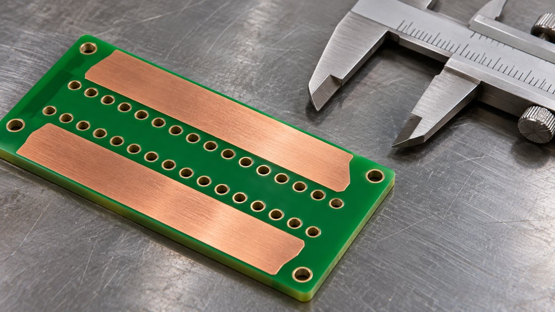
Bare PCB coupon with rows of plated through holes
AI-generated illustration of via geometry, not a current or temperature test.

Check How Current Leaves on the Other Layer

A balanced top feed can still become an uneven array if the bottom exit favors one edge. Inspect the receiving copper and any plane voids, slots or clearances. Run the source-to-load path in the correct direction; looking at only one layer can hide the limiting geometry.

Use a Single-Via Tool for the Right Question

A barrel estimate is useful for first-pass geometry checks. The Best Technology via current calculator addresses via sizing; do not treat a result as proof that multiplying by the via count gives the array’s continuous rating. Review path resistance and board-level thermal behavior separately.

Check Local Heating and Shared Copper

An individual branch can be overloaded even when the total drop looks acceptable. Conversely, evenly loaded vias can all heat if their surrounding copper shares a poor heat path. Review the complete board under the specified load, ambient, enclosure and cooling conditions.

Decide When a Distributed Model Is Needed

If the pours share substantial copper, the simple two-branch model is only a teaching aid. Use an appropriate extraction or field model to compare current density through the copper and vias. For fast switching, include loop inductance and return geometry rather than extending the DC result to all frequencies.

Verify the First Board Under a Defined Load

Compare predicted drop and heating with an approved board test at the intended duty cycle. Record the voltage sense locations, ambient, airflow and temperature observation method. If a hot region appears, inspect the current path and setup before assuming the closest via is the only cause.

Release Geometry and Acceptance Together

Document the power path, layer transitions, finished via construction, minimum relevant copper, and the actual verification limits. If changing the drill, plating or copper exit, reassess both electrical loss and temperature. An identical via count is not evidence that the updated board behaves the same.

FAQ

Do six vias always carry twice as much as three?

No. More vias add possible paths, but they do not remove a common bottleneck or guarantee balanced current. Compare the feed and exit geometry, barrel dimensions and heat paths. Validate the actual array under its operating conditions instead of multiplying an isolated-via number.

Does a via near the connector always carry the most?

No. Distance from the connector is only one clue. Both the incoming and outgoing copper, their widths, and any shared constrictions matter. A nearby via with a poor exit may carry less than a farther one with a lower complete path resistance.

Is via plating thickness the same as outer copper weight?

Not necessarily. The finished wall plating and the outer layer copper are different manufacturing quantities. Request the finished barrel requirement that applies to the holes you are using. Using a foil weight as a substitute for a wall thickness can distort the calculation.

Does a wider finished hole always lower total path resistance?

It can increase barrel cross-section for a given plating thickness, but the surrounding copper and allowed clearances may also change. Evaluate the entire connection, not the hole alone. A larger barrel does not fix a narrow copper neck immediately before or after it.

Can I confirm current sharing with a thermal camera alone?

No. Temperature reflects heating and cooling, and nearby parts or copper can obscure the source. Use the image as a diagnostic clue, compare it with an electrical model or suitable measurements, and record the observation conditions. Do not infer branch current directly from surface color.

Does filling the hole with solder make the calculation unnecessary?

No. The resulting fill and current path may not be controlled as assumed, and the surrounding copper still matters. Do not claim an amp rating from visual fill. Use the specified via construction and evidence appropriate to the actual board and operating load.

Do DC results apply to pulsed current?

Not in general. Heating depends on the duty and thermal response, while fast edges can make inductance and return geometry important. Use the actual pulse conditions and an appropriate model or test before treating a DC split as a reliable prediction for switching operation.

What should be shared with a board supplier?

Provide the layer stack, drill and plating requirements, power path artwork, load and duty, and acceptance plan. Point out narrow sections near the array rather than sending only a via count. The supplier can review buildability, while the design owner retains responsibility for validating system operation.

Prepare a Power Layout Review

Send the layer stack, finished via requirements, layout revision and load assumptions to the Best Technology team.

You may also like