A lab measures a PCB trace through two coax launches. The displayed result includes whatever lies between the measurement reference planes, not necessarily the trace alone. De-embedding estimates the response of the trace by removing a characterized fixture model. If the model does not match the real fixture, the corrected curve can be misleading.
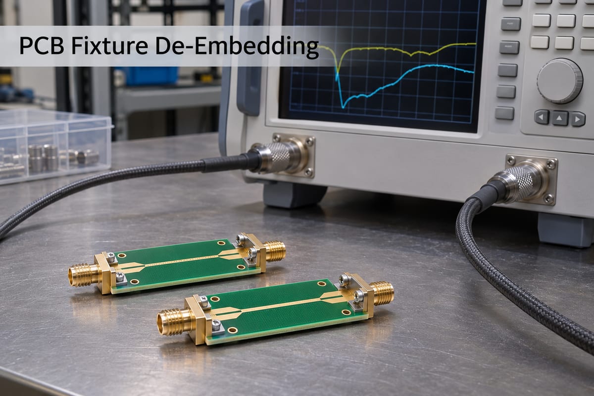
Start with one question: what is the device under test?
Suppose you want the loss of a straight trace on a radio board, excluding both connector launches. Call that trace the device under test, or DUT. If you instead want the loss of the assembled connector-to-connector board, the launches are part of the DUT. Both measurements are valid when clearly labeled.
What a reference plane means
A reference plane is the electrical boundary at which the measurement is defined. In this example, cable-end calibration may leave the launch and short lead-in traces inside the reported measurement. Mark the desired boundaries on the coupon drawing before interpreting a plot.
Calibration versus fixture removal
Calibration addresses the measuring system at the chosen planes. Fixture removal uses a model of the physical structure between those planes and the desired DUT boundaries. These operations are related but not interchangeable. Record both the calibration and fixture treatment used.
Why subtracting one number is not a general fix
A launch can reflect energy, so multiple reflections can affect the measured response. Adding or subtracting a fixed loss number does not generally remove those interactions. Use a model appropriate to the port arrangement and band, not a single correction guessed from a datasheet.
How a 2x Thru coupon helps
A 2x Thru joins representative fixture sections without the intended DUT. Measuring it gives an appropriate extraction method information about the fixture halves. In the radio-board example, the left and right launches on that reference structure must represent the corresponding launches in the DUT measurement.
Detailed measurement parameters to record
For an illustrative two-port job, document the intended sweep, for example 1–6 GHz, the reference impedance, for example 50 Ω, and the direction defined as port 1 to port 2. These are teaching inputs, not a universal requirement or measured result. S21 describes forward transmission under its stated reference conditions; display convention matters when comparing negative transmission in dB with positive insertion loss.
| Measurement boundary | What the result includes |
| Cable ends | The launches and board path between the cable ends. |
| Trace ends | The intended trace response after valid calibration or fixture treatment. |
Choose between raw data, a model and calibration standards
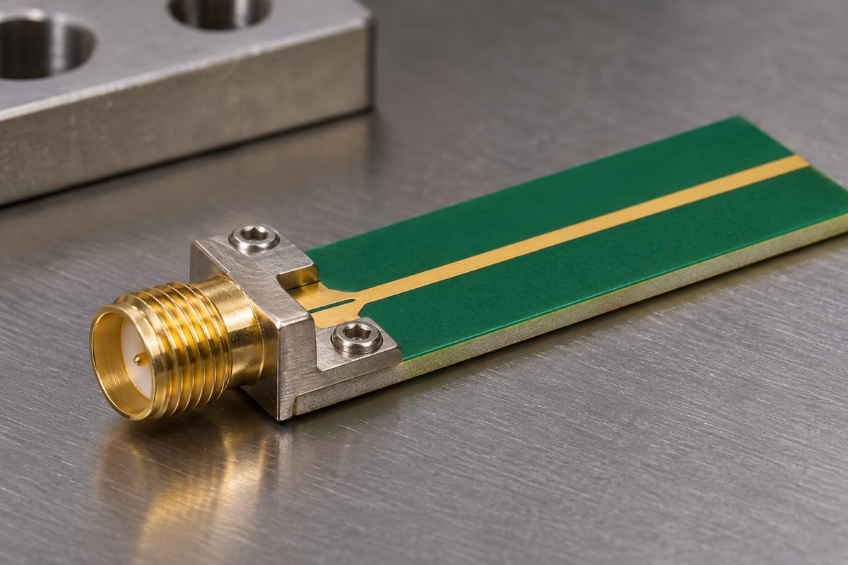
Keep raw connector-to-connector data when those connectors are part of the product. Use a validated fixture model if you need the trace alone. A suitable calibration structure can instead set planes closer to the DUT. Which approach works depends on what standards or fixture structures can actually be made and characterized.
Make the reference coupon representative
Review stackup, launches, connector footprint, routing and local ground connections. A shorter trace on different material is not automatically a matching fixture. Keep the drawing revision and the as-built differences with the test record.
Check port numbering and fixture direction
Left and right fixture files may not be interchangeable. Confirm where each file starts and ends and whether its port order matches the instrument workflow. When the curve looks implausible, check this mapping before changing the board design.
| Input | Illustrative setting, not a limit |
| Frequency range | 1–6 GHz in the example test plan. |
| Reference impedance | 50 Ω in the example. |
| Forward direction | Port 1 to port 2; report as S21 with the chosen display convention. |
Recognize a correction that cannot be trusted
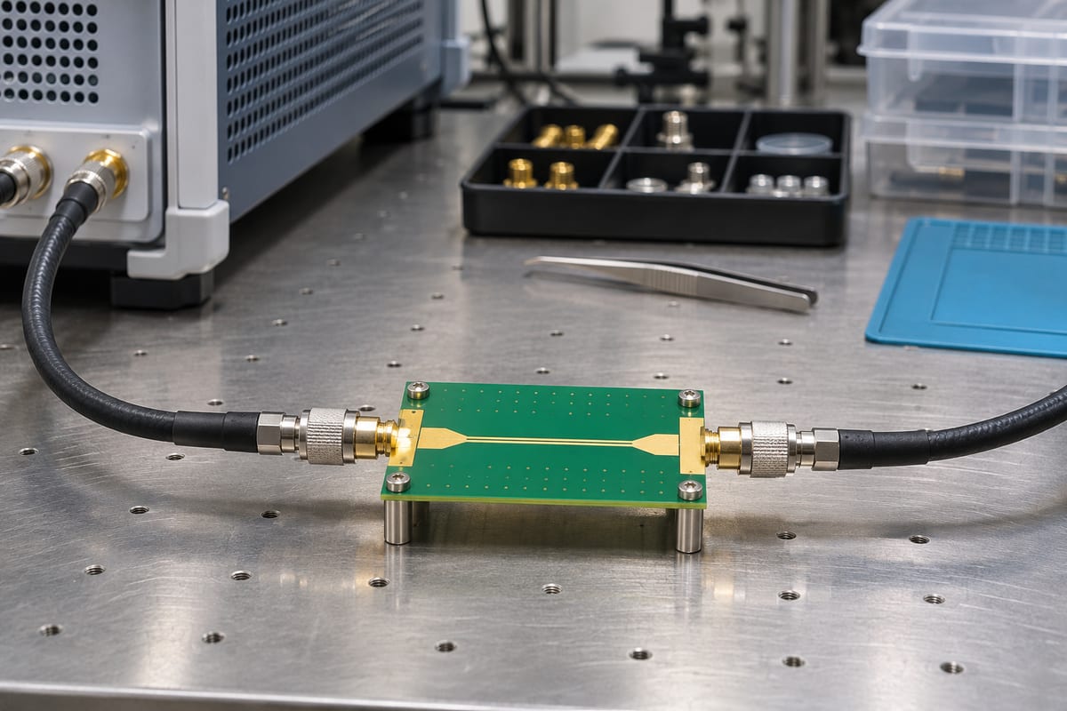
Unexpected apparent gain on a passive trace or a sharp feature not present in repeat tests warrants investigation. Check calibration, connection repeatability, fixture bandwidth and model quality. Do not treat a smooth curve alone as evidence that the correction is sound.
Compare measurements at identical boundaries
When comparing to simulation, define the same electrical length and reference planes. A model ending at the trace boundaries will not match a measurement that still includes the launches. Save both raw and corrected files so another engineer can see exactly what changed.
Release the test plan with the PCB
Include the DUT and reference coupon geometry, intended band, calibration setup, port mapping, model limits and acceptance basis. If the fixture is not representative, keep the result labeled as a combined measurement until the missing evidence is resolved.
FAQ
Should I always remove the connectors from the result?
No. If your deliverable is a complete connector-to-connector assembly, the launches may belong in the device under test. If the question is trace loss alone, define trace-end reference planes instead. Label the result so it is not compared with a measurement made at different boundaries.
Is a 2x Thru simply the DUT trace cut in half?
No. Its purpose is to represent the fixture sections joined without the intended device under test. How it is constructed and interpreted depends on the extraction method. Match the launches and interfaces to those on the DUT coupon, and document assumptions rather than relying on the name alone.
Can I reuse fixture files from another board revision?
Only after showing that the revised geometry and measurement setup still match the characterized fixture sufficiently for the task. A moved connector, different stackup or changed launch may alter the response. Retain the fixture file revision with the raw data so the comparison can be repeated.
Why can a passive trace appear to have gain?
A correction can amplify errors when the fixture model, measurement band or port mapping is unsuitable. Investigate the setup and repeatability rather than assuming the trace provides power gain. Compare the raw data and the characterized fixture before applying the corrected result to a release decision.
Does cable-end calibration remove a board launch?
Not by itself if the launch lies inside the calibrated measurement boundaries. Decide whether that launch is part of the reported device or needs a suitable fixture treatment. Record where the planes are set; calibration at the cable ends does not establish that the reported curve is trace-only.
Can I compare the corrected curve directly with any simulation?
Only after checking that simulation and measurement use matching reference planes, geometry, port direction and reference conditions. A trace-length or launch mismatch can produce differences unrelated to material quality. Keep both raw and processed measurements to make the comparison and its limitations transparent.
Can I use just a single loss number for the fixture?
A fixed correction may omit reflections, phase and variation with frequency. It is not a general replacement for a characterized fixture model. If a simplified method is used, state its assumptions and scope, and verify that it is adequate for the decision being made.
What files should the test team keep?
Keep the coupon drawings, raw measurements, fixture or calibration data, corrected files, port map and method settings. Record the board revision and test band. If the result is compared to a limit, preserve the requirement and the reference planes so someone else can reproduce the decision.
References
Primary technical reference · Related technical guide
For a build discussion, share the drawing and acceptance requirements with sales@bestpcbs.com.