PCB manufacturing PCB manufacturing
Home > Blog

pcb test coupon

Microvia Reliability: Read the Reflow Resistance Trace
Tuesday, November 10th, 2026

Don’t release an HDI lot on the strength of a cold continuity check alone when the purchase requirements call for reflow-monitored resistance. First verify that the coupon reproduces the critical via structure. Then compare its resistance trace with the agreed reference and temperature profile. A chain can read normally after cooling even if it opened during heating.

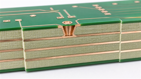
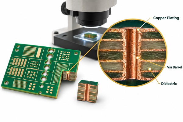
Mounted PCB cross-section with copper interconnections and dielectric layers
Illustrative rendering of a cross-section specimen. Use the actual stack drawing and coupon record to identify via geometry.

microvia reliability

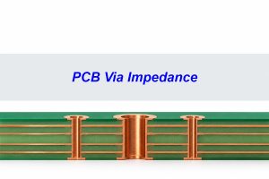
Microvias connect adjacent PCB layers in dense layouts. During soldering, the board expands and contracts, stressing these connections. A room-temperature continuity result answers whether the path conducts at that moment. It does not reveal an interruption that occurs only at elevated temperature. Ask for the evidence that matches the anticipated assembly exposure.

stacked vs staggered microvias

A stacked design places one microvia above another. A staggered design offsets them and joins the paths on a shared layer. When the board uses both, identify which geometry each coupon actually represents. A result from a staggered chain should not be used to approve an unrepresented stacked interface. For routing and construction trade-offs, see the BestPCBs comparison guide.

Board feature Check on the coupon
Stacked microvias Same layer spans and stacked interface
Staggered microvias Correct layer spans and offset pattern
Mixed connections Coverage of each structure required for release

pcb daisy chain

A daisy chain connects many via structures in series so that a change anywhere in the path can appear in the resistance record. Ask for the chain ID, layer pairs, structure count and panel-to-coupon relationship. The resulting trace describes the chain, not the resistance or failure location of an individual via. A chain that includes other structures may require fault isolation.
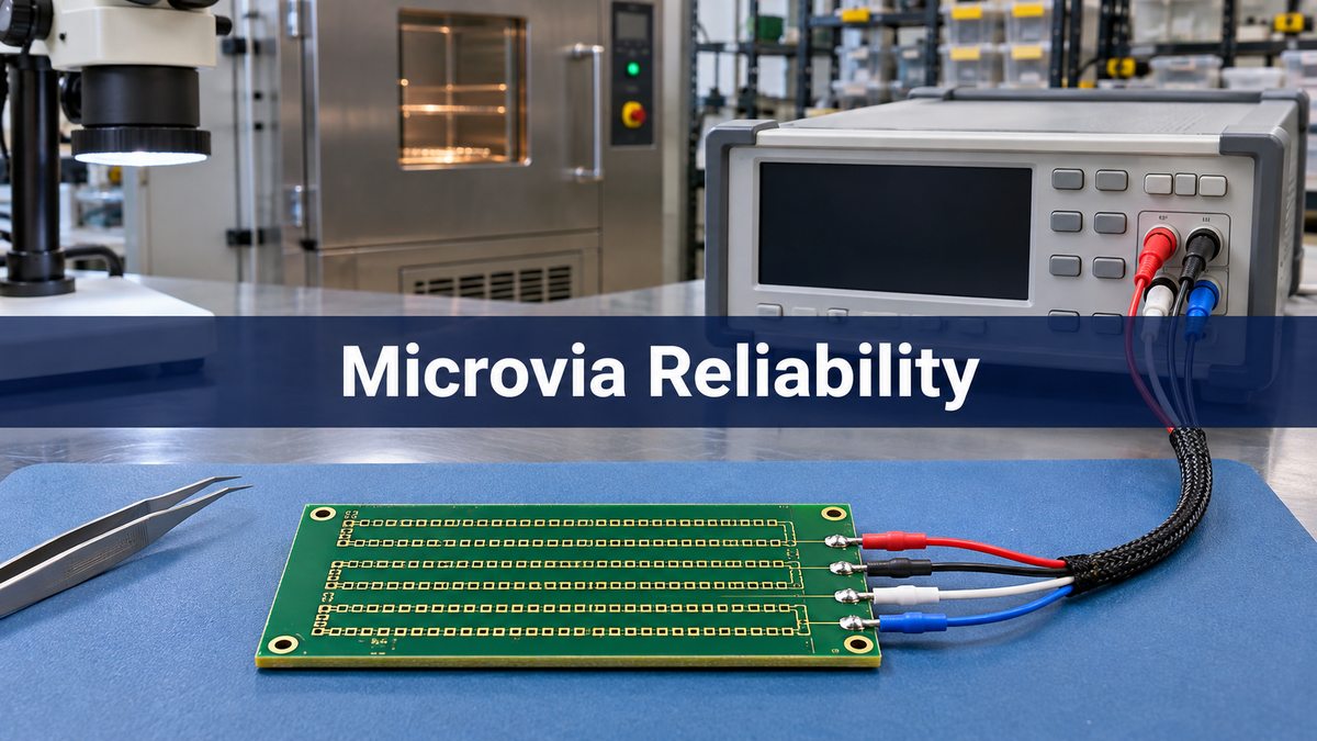
Bare test coupon and measurement leads on an electronics lab bench
Illustrative rendering of a coupon setup, not a test log or a pass result.

pcb reflow profile

Compare traces only under the approved profile and measurement convention. Record the test method and revision, profile, cycle count, temperature measurement location and reference resistance. For a performance-based evaluation under IPC-TM-650 2.6.27, use the reference and acceptance criteria in the applicable revision and procurement agreement. Do not silently substitute a cold baseline for a specified hot reference.

Report field Why it matters
Profile and cycle Matches the specified exposure
Resistance in Ω or mΩ Identifies the measured chain and reference
Change in % Shows the result at the specified comparison point
Temperature and time Locates the event within the cycle

microvia failure

Consider an illustrative chain with a specified hot reference of 0.500 Ω. A comparable point in a later cycle reads 0.530 Ω. The relative rise is (0.530 − 0.500) ÷ 0.500 = 6%. If the project limit were 5%, the reading would exceed it. A normal cold reading afterward does not cancel the event. These values are a worked example, not a test report or a universal limit.

Check whether the event is synchronized with temperature and whether other channels show a simultaneous fixture disturbance. Preserve the original trace and reference coupon. When instrumentation remains a plausible cause, use the documented investigation or retest procedure instead of deleting the event or releasing on the final reading alone.

pcb microsection analysis

Use the electrical record to choose where to section. A section can show a physical discontinuity at a sampled interface, but a clean section elsewhere cannot rule out a hot-only failure in the chain. Ask the lab to correlate the section location with the failed net, stack and panel rather than accepting an unlabeled image.

interconnect stress test pcb

Convection reflow simulation reproduces an agreed assembly heat exposure. DC current-induced thermal cycling is a different test method with a different heating mechanism and protocol. Don’t accept one in place of the other simply because both include resistance readings. Match the report to the contracted exposure, specimen and evaluation method.

pcb thermal cycling test

Specify separately any cycling needed to qualify the board for service. A reflow simulation result alone does not establish lifetime under operational temperature changes. For lot release, verify the approved coupon map, profile, complete trace and disposition of any anomalies. If the controlling geometry or hot record is missing, mark the evidence incomplete rather than treating the omission as a pass.

FAQ

Is the final resistance value enough?

No when the requirement covers behavior during the cycle. Inspect the agreed measurement interval and preserve any anomalous excursion.

Can an unmarked coupon represent every panel?

Not without documented traceability and an agreed sampling plan. Link its identity to the appropriate panel, lot and build.

Does a resistance excursion prove a microvia crack?

No. It locates a suspect time and chain. Check the test setup and use targeted failure analysis before assigning a cause.

Can I compare two chains with different numbers of vias directly?

Not by raw resistance alone. Geometry and chain length affect the value. Use the prescribed baseline and compare equivalent structures where possible.

Does a passed stacked coupon qualify a deeper stack?

Not automatically. Additional interfaces and different layers can change the behavior. Confirm that the evidence represents the intended construction.

Does the oven setpoint equal coupon temperature?

No. Confirm the recorded measurement convention and coupon temperature rather than assuming the displayed setting is the specimen profile.

Can I approve the lot if the report only says pass?

Only if that is sufficient under the agreement. When the purchase requires traces, conditions or specimen details, request the missing evidence before release.

What should I retain for a repeat order?

Keep the approved stack, coupon ID and drawing, reference convention, test profile, original records and disposition together with the production revision.

Sources

IPC-TM-650 2.6.27B: convection reflow assembly simulation; IPC-TM-650 2.6.26A: DC current-induced thermal cycling.

Project Review

For a Best Technology fabrication discussion, send the critical via stack, intended assembly exposure and coupon acceptance requirements to sales@bestpcbs.com.

You may also like

PCB Fixture De-Embedding: Is the Loss in the Trace?
Friday, November 6th, 2026

A lab measures a PCB trace through two coax launches. The displayed result includes whatever lies between the measurement reference planes, not necessarily the trace alone. De-embedding estimates the response of the trace by removing a characterized fixture model. If the model does not match the real fixture, the corrected curve can be misleading.

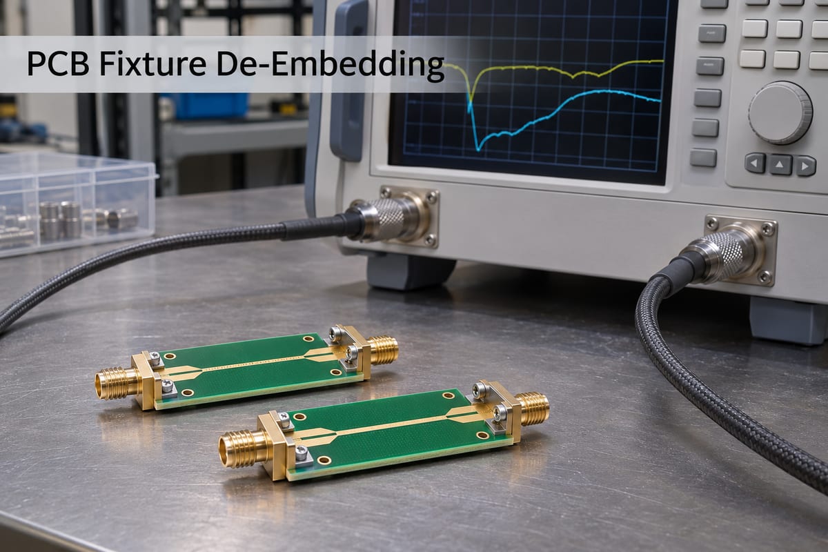
Two PCB coupons beside a lab instrument
AI-generated illustration. The screen traces are fictional and do not show measured PCB loss or de-embedding results.

Start with one question: what is the device under test?

Suppose you want the loss of a straight trace on a radio board, excluding both connector launches. Call that trace the device under test, or DUT. If you instead want the loss of the assembled connector-to-connector board, the launches are part of the DUT. Both measurements are valid when clearly labeled.

What a reference plane means

A reference plane is the electrical boundary at which the measurement is defined. In this example, cable-end calibration may leave the launch and short lead-in traces inside the reported measurement. Mark the desired boundaries on the coupon drawing before interpreting a plot.

Calibration versus fixture removal

Calibration addresses the measuring system at the chosen planes. Fixture removal uses a model of the physical structure between those planes and the desired DUT boundaries. These operations are related but not interchangeable. Record both the calibration and fixture treatment used.

Why subtracting one number is not a general fix

A launch can reflect energy, so multiple reflections can affect the measured response. Adding or subtracting a fixed loss number does not generally remove those interactions. Use a model appropriate to the port arrangement and band, not a single correction guessed from a datasheet.

How a 2x Thru coupon helps

A 2x Thru joins representative fixture sections without the intended DUT. Measuring it gives an appropriate extraction method information about the fixture halves. In the radio-board example, the left and right launches on that reference structure must represent the corresponding launches in the DUT measurement.

Detailed measurement parameters to record

For an illustrative two-port job, document the intended sweep, for example 1–6 GHz, the reference impedance, for example 50 Ω, and the direction defined as port 1 to port 2. These are teaching inputs, not a universal requirement or measured result. S21 describes forward transmission under its stated reference conditions; display convention matters when comparing negative transmission in dB with positive insertion loss.

Measurement boundary What the result includes
Cable ends The launches and board path between the cable ends.
Trace ends The intended trace response after valid calibration or fixture treatment.
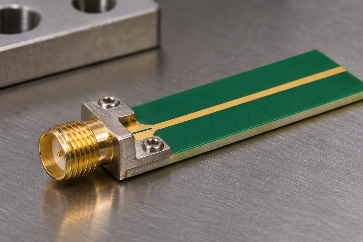
PCB fixture illustration 2
AI-generated physical illustration; not a company sample or a measurement record.

Choose between raw data, a model and calibration standards

Keep raw connector-to-connector data when those connectors are part of the product. Use a validated fixture model if you need the trace alone. A suitable calibration structure can instead set planes closer to the DUT. Which approach works depends on what standards or fixture structures can actually be made and characterized.

Make the reference coupon representative

Review stackup, launches, connector footprint, routing and local ground connections. A shorter trace on different material is not automatically a matching fixture. Keep the drawing revision and the as-built differences with the test record.

Check port numbering and fixture direction

Left and right fixture files may not be interchangeable. Confirm where each file starts and ends and whether its port order matches the instrument workflow. When the curve looks implausible, check this mapping before changing the board design.

Input Illustrative setting, not a limit
Frequency range 1–6 GHz in the example test plan.
Reference impedance 50 Ω in the example.
Forward direction Port 1 to port 2; report as S21 with the chosen display convention.
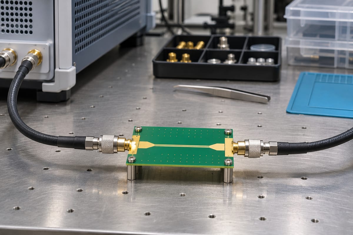
PCB fixture illustration 3
AI-generated physical illustration; not a company sample or a measurement record.

Recognize a correction that cannot be trusted

Unexpected apparent gain on a passive trace or a sharp feature not present in repeat tests warrants investigation. Check calibration, connection repeatability, fixture bandwidth and model quality. Do not treat a smooth curve alone as evidence that the correction is sound.

Compare measurements at identical boundaries

When comparing to simulation, define the same electrical length and reference planes. A model ending at the trace boundaries will not match a measurement that still includes the launches. Save both raw and corrected files so another engineer can see exactly what changed.

Release the test plan with the PCB

Include the DUT and reference coupon geometry, intended band, calibration setup, port mapping, model limits and acceptance basis. If the fixture is not representative, keep the result labeled as a combined measurement until the missing evidence is resolved.

FAQ

Should I always remove the connectors from the result?

No. If your deliverable is a complete connector-to-connector assembly, the launches may belong in the device under test. If the question is trace loss alone, define trace-end reference planes instead. Label the result so it is not compared with a measurement made at different boundaries.

Is a 2x Thru simply the DUT trace cut in half?

No. Its purpose is to represent the fixture sections joined without the intended device under test. How it is constructed and interpreted depends on the extraction method. Match the launches and interfaces to those on the DUT coupon, and document assumptions rather than relying on the name alone.

Can I reuse fixture files from another board revision?

Only after showing that the revised geometry and measurement setup still match the characterized fixture sufficiently for the task. A moved connector, different stackup or changed launch may alter the response. Retain the fixture file revision with the raw data so the comparison can be repeated.

Why can a passive trace appear to have gain?

A correction can amplify errors when the fixture model, measurement band or port mapping is unsuitable. Investigate the setup and repeatability rather than assuming the trace provides power gain. Compare the raw data and the characterized fixture before applying the corrected result to a release decision.

Does cable-end calibration remove a board launch?

Not by itself if the launch lies inside the calibrated measurement boundaries. Decide whether that launch is part of the reported device or needs a suitable fixture treatment. Record where the planes are set; calibration at the cable ends does not establish that the reported curve is trace-only.

Can I compare the corrected curve directly with any simulation?

Only after checking that simulation and measurement use matching reference planes, geometry, port direction and reference conditions. A trace-length or launch mismatch can produce differences unrelated to material quality. Keep both raw and processed measurements to make the comparison and its limitations transparent.

Can I use just a single loss number for the fixture?

A fixed correction may omit reflections, phase and variation with frequency. It is not a general replacement for a characterized fixture model. If a simplified method is used, state its assumptions and scope, and verify that it is adequate for the decision being made.

What files should the test team keep?

Keep the coupon drawings, raw measurements, fixture or calibration data, corrected files, port map and method settings. Record the board revision and test band. If the result is compared to a limit, preserve the requirement and the reference planes so someone else can reproduce the decision.

References

Primary technical reference · Related technical guide

For a build discussion, share the drawing and acceptance requirements with sales@bestpcbs.com.

You may also like

PCB Test Coupons: Types, Testing & IPC Guide
Thursday, September 17th, 2026

PCB test coupons are representative test structures placed on the same fabrication panel as the production boards. They are built with the same materials, copper plating, lamination, drilling, and other key processes so manufacturers can verify characteristics such as controlled impedance, plated-hole quality, via reliability, registration, and solderability without cutting into the finished PCB.

Different PCB test coupons serve different purposes. Impedance coupons are commonly checked with TDR, while structural coupons can be microsectioned to inspect plating and internal alignment. The coupon design should reflect the actual production stackup and fabrication process.

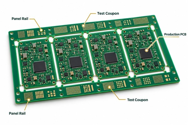
PCB test coupons integrated into the panel rail of a production PCB panel

What Is a PCB Test Coupon?

A PCB test coupon is a dedicated test structure manufactured on the same panel as the production PCB to represent selected features of the finished board.

Unlike the functional PCB, the coupon is created specifically for inspection or measurement. Depending on the requirement, it may reproduce:

  • Controlled-impedance traces
  • Plated through holes
  • Microvias or blind vias
  • Internal layer registration features
  • Copper plating structures
  • Solderability features

The key point is representation. A useful coupon should experience the same relevant fabrication processes as the board it is intended to represent.

PCB test coupons are commonly placed in the panel rail or other non-product area, so testing does not consume a usable PCB.

At EBest Circuit, coupon requirements can be reviewed together with the production stackup during DFM. For controlled-impedance, HDI, RF, or high-reliability boards, this helps keep the test structure aligned with the actual PCB manufacturing conditions.

Why Are Test Coupons Used Instead of Testing the Production PCB?

PCB test coupons allow measurements and destructive inspections to be performed without damaging the production board.

Some verification methods cannot be carried out conveniently on a finished PCB. Microsection analysis, for example, requires the sample to be cut, mounted, polished, and inspected under magnification.

Coupons also provide a more consistent structure for tests such as TDR because production routing may contain:

  • Vias
  • Pads
  • Connectors
  • BGA breakouts
  • Plane changes
  • Short trace segments

These features can make measurement results harder to interpret.

A dedicated coupon can reproduce the required stackup and trace geometry while providing enough length and accessible test points for repeatable measurement.

The coupon therefore does not replace electrical or functional testing of the PCB. It provides process evidence for specific fabrication characteristics.

What Types of PCB Test Coupons Are Commonly Used?

PCB test coupon types are usually selected according to what needs to be verified rather than by using one universal coupon design.

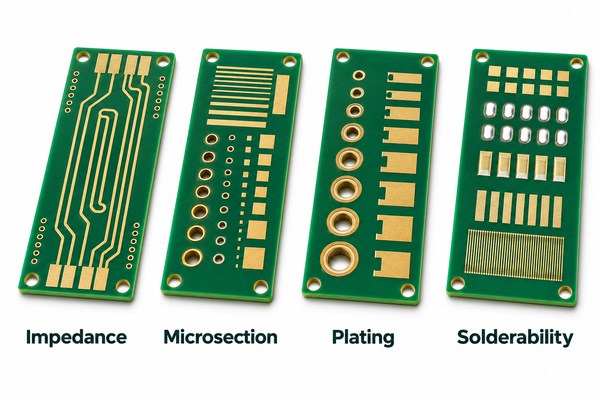
Coupon / Test Structure What It Checks Typical Test Method
Impedance coupon Single-ended or differential impedance TDR
PTH structural coupon Hole wall plating and registration Microsection
Via reliability coupon Via or interconnect integrity Thermal stress / resistance monitoring
Microvia coupon HDI microvia quality and stacking Microsection / reliability test
Solderability coupon Solder wetting performance Solderability test
Peel-strength coupon Copper adhesion Peel test
SIR coupon Surface insulation resistance Electrical resistance testing

Some IPC qualification and conformance structures use letter-based coupon designations. However, for most PCB buyers and engineers, the more useful question is not the letter itself but what manufacturing characteristic the coupon is intended to verify.

Common PCB test coupon types including impedance plated through-hole microvia via reliability solderability and SIR coupons

What Can PCB Test Coupons Verify?

PCB test coupons can verify several manufacturing characteristics that are difficult to confirm from visual inspection alone.

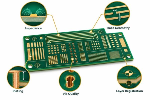
Common checks include:

  • Controlled impedance
  • Copper plating thickness
  • Plated through-hole integrity
  • Microvia quality
  • Annular ring condition
  • Internal layer registration
  • Solderability
  • Copper adhesion
  • Interconnect reliability

For example, an impedance coupon can confirm whether a nominal 50 Ω or 100 Ω structure is within tolerance after lamination, plating, and etching.

A microsection coupon serves a different purpose. It allows the manufacturer to inspect the actual cross-section of a plated hole or via and evaluate conditions such as copper distribution, registration, and interface quality.

PCB test coupon illustrating impedance trace geometry plating via quality and layer registration verification

Where Are Test Coupons Located on a PCB Panel?

PCB test coupons are usually placed in the panel rail or another non-functional area of the production panel.

This position allows the coupon to travel through the same major fabrication processes as the PCBs while remaining separate from the customer’s usable board outline.

A useful coupon should be positioned so that it represents the production process as closely as practical, especially for:

  • Lamination
  • Drilling
  • Copper plating
  • Etching
  • Surface treatment

Coupon placement also needs to leave enough room for test access, sectioning, or removal from the panel.

For controlled-impedance production, the coupon is typically designed around the same layer pair, dielectric thickness, copper condition, and trace geometry used by the actual impedance-controlled routing.

PCB panel showing test coupons located in the top and bottom panel rails

How Are Impedance Test Coupons Tested with TDR?

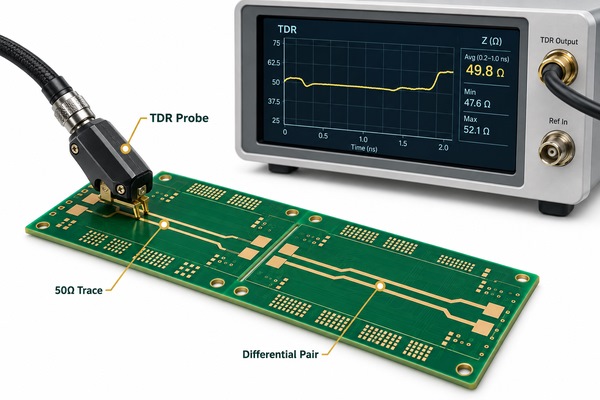
An impedance test coupon reproduces the controlled-impedance structure of the production PCB so its characteristic impedance can be measured with time-domain reflectometry, or TDR.

The coupon normally represents the same:

  • Signal layer
  • Reference plane
  • Dielectric thickness
  • Copper thickness
  • Trace width
  • Differential spacing, where applicable
  • Material system

During TDR testing, a fast electrical edge is launched into the coupon. The instrument measures reflections along the transmission line and converts them into an impedance profile.

The result is then compared with the specified target, such as:

  • 50 Ω single-ended
  • 90 Ω differential
  • 100 Ω differential

A typical tolerance may be ±10%, although tighter limits can be specified.

The coupon should be based on the final production stackup rather than only the original CAD trace width. Plating, etching, dielectric thickness, and manufacturing compensation can all change the finished impedance.

PCB impedance test coupon connected to TDR equipment for controlled impedance verification

How Are Test Coupons Used for Microsection and Via Inspection?

Microsection coupons are cut and polished so the internal PCB structure can be inspected directly under magnification.

This method is commonly used to evaluate plated through holes, blind vias, microvias, and multilayer registration.

A typical microsection can reveal:

  • Hole-wall copper thickness
  • Copper distribution
  • Annular ring condition
  • Layer-to-hole registration
  • Resin condition
  • Via interfaces
  • Microvia geometry
  • Lamination quality

Because the coupon is intentionally sacrificed, the production PCB remains intact.

For HDI boards, microsection inspection is especially useful because microvias, stacked structures, and thin dielectric layers can create manufacturing risks that are not visible from the board surface.

Microsection results should be interpreted against the relevant drawing, customer specification, and applicable IPC acceptance requirements rather than treated as a generic pass/fail image.

PCB microsection showing plated through hole microvia copper layers annular ring and resin

Who Should Design PCB Test Coupons—the Designer or the Fabricator?

PCB test coupon design is typically a shared responsibility: the PCB designer defines the electrical and reliability requirements, while the fabricator finalizes the coupon structure for the actual production process.

The customer should provide requirements such as:

  • Target impedance
  • Impedance tolerance
  • Stackup constraints
  • Material requirement
  • Via structure
  • Reliability requirement
  • Required reports or inspection records

The fabricator then knows the actual production details, including dielectric availability, drill size, finished copper thickness, plating allowance, and etching compensation.

For that reason, it is often better for the PCB manufacturer to create or adjust the coupon after the production stackup is confirmed.

If a customer-supplied coupon is included in the fabrication data, it should still be reviewed during DFM to make sure it matches the manufacturing stackup and test method.

Engineer reviewing PCB stackup impedance and test coupon requirements during DFM

What Test Coupon Requirements Should You Include in Your PCB RFQ?

A PCB RFQ should clearly state what needs to be verified rather than simply asking for “test coupons.”

For controlled-impedance or high-reliability projects, provide:

  • Gerber or ODB++ files
  • PCB stackup or stackup constraints
  • Material grade
  • Finished board thickness
  • Copper weight
  • Target impedance
  • Single-ended or differential requirement
  • Impedance tolerance
  • Critical routing layers
  • Via or microvia structure
  • Required test reports
  • Whether physical coupons should be returned

For example, “50 Ω controlled impedance required” is less useful than specifying the routing layer, reference plane, stackup requirement, and tolerance.

FAQ About PCB Test Coupons

1. Is a PCB test coupon part of the finished PCB? No. It is normally placed in the panel rail or another non-product area and removed from the production panel.

2. Do I need to include a test coupon in my Gerber files? Not always. In many projects, the customer provides the test requirement and the PCB manufacturer creates the coupon based on the final production stackup.

3. What is an impedance test coupon? It is a representative transmission-line structure used to measure the finished PCB impedance, commonly with TDR.

4. Can a test coupon prove that every PCB on the panel is good? No. A coupon provides representative process evidence for specific characteristics. It does not replace board-level inspection or electrical testing.

5. Are PCB test coupons normally sent to the customer? They can be. Whether physical coupons, TDR reports, microsection images, or other records are supplied should be defined in the order or quality requirement.

6. What information should I provide for controlled-impedance coupon testing? Provide the target impedance, tolerance, routing layer, reference plane, stackup, material, copper weight, and any special coupon or reporting requirements.

Ready to Review Your PCB Test Coupon Requirements?

PCB test coupons are most useful when they are tied to a specific manufacturing risk, whether that is impedance, plating, microvia quality, registration, or another measurable characteristic. Defining the test requirement before production makes the coupon more representative and the resulting data more useful.

EBest Circuit supports controlled-impedance, HDI, RF, multilayer PCB manufacturing, PCBA, DFM review, TDR testing, and microsection inspection. For projects that require coupon-based verification, send your Gerber files and PCB specifications to sales@bestpcbs.com. Our engineering team can review the stackup, test requirements, and coupon approach before fabrication.

After coupon results are approved, our SMT assembly workflow can also coordinate circuit board stencil requirements with the released fabrication data.

You may also like