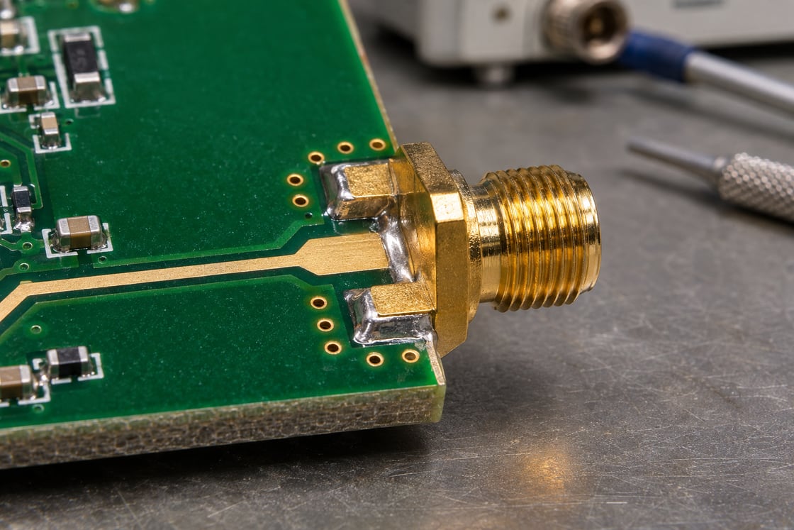
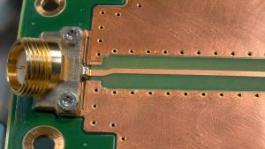
On a grounded coplanar waveguide (GCPW), the electric field extends into the gaps beside the signal trace. Changing solder mask there changes the dielectric environment, even if the copper artwork stays the same. Model the actual coverage and test a representative structure before using the result in an RF design.
Where the Electric Field Goes
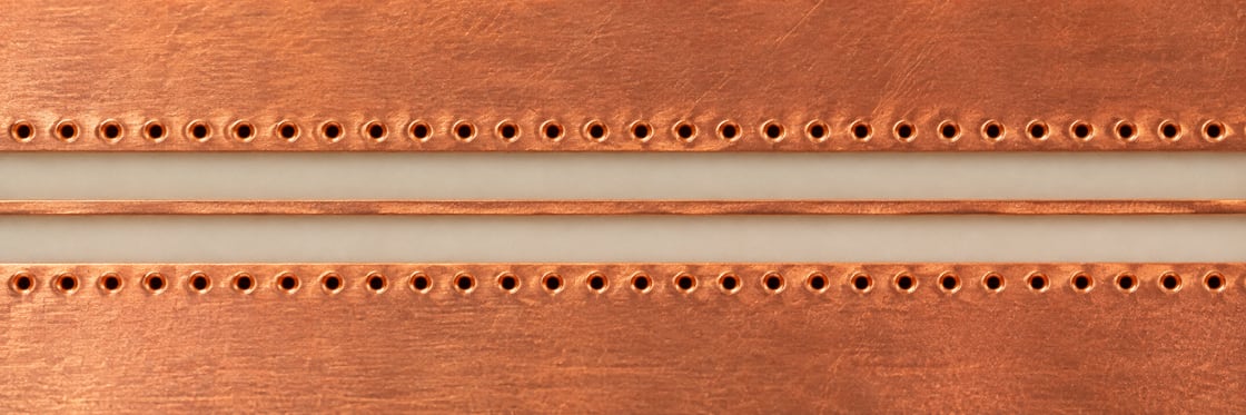
A GCPW has a surface signal between nearby ground copper and a reference plane underneath. Some of the field lies near the surface gaps rather than entirely in the laminate. Rogers’ comparison of microstrip and GCPW explains the different structures.
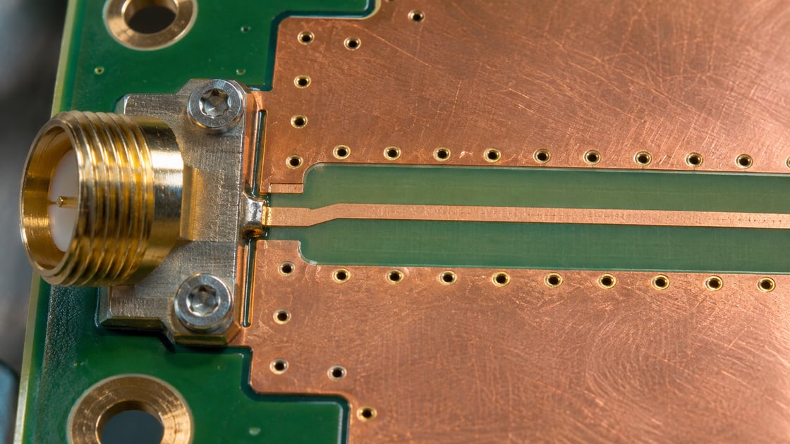
What Solder Mask Changes
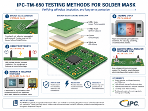
Mask replaces some air with a dielectric. That can alter the field distribution, characteristic impedance, phase and loss. Rogers’ millimetre-wave fabrication paper discusses insertion-loss and phase effects; the size of the effect depends on the construction.
Detailed Inputs for the Solver
| Input | Unit or record | Why it matters |
| — | — | — |
| Finished signal width | mm | Sets conductor geometry |
| Lateral gap | mm, both sides | Defines coupling to surface ground |
| Reference spacing | mm | Describes coupling below the trace |
| Mask shape | Thickness and lateral extent | Defines dielectric coverage |
| Material properties | Dk and Df with frequency | Defines electrical inputs |
Mask Over the Gap vs an Open Window
| Construction | Primary check | Other trade-off |
| — | — | — |
| Continuous mask | Model trace top and gaps | May protect exposed copper |
| Open RF window | Model air and actual finish | Review handling and assembly |
| Local mask dam | Model the transition if relevant | Check registration and solder control |
Do Not Apply One Thickness Everywhere
Mask thickness above a conductor may differ from its coverage beside the copper. Ask how the cross-section is represented in the solver and what the fabricator can substantiate. A single thickness copied from a catalogue may not describe the lateral gap.
Example: A Launch Opens but the Route Stays Covered
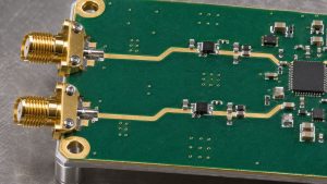
Consider a hypothetical RF launch whose pad is exposed, followed by a masked line. The mask boundary creates a local change in environment even though the straight line width is constant. Compare the continuous covered section, the opening and the boundary rather than modeling only one cross-section.
Use a Two-Dimensional Model for the Uniform Section
A cross-section solver can compare uniform masked and unmasked geometries with other inputs held constant. It is not a full model of the launch or a short mask island. Use an appropriate three-dimensional or measured comparison if the transition determines performance.
Review the Finish Alongside Mask Removal
Opening a window can expose a finished surface that differs from the original modeled conductor. Include the specified finish and assembly requirements in the comparison. Do not attribute every measured loss change to the absence of mask when other features changed too.
Check Mask Registration Against the Gap
Mark the intended opening in the artwork and compare the alignment tolerance with the clearance from the signal and adjacent ground. Check both sides. A boundary intended to be symmetric can move and create an asymmetric structure.
Use a Coupon That Represents the Actual Coverage
Specify the same relevant width, gap, stackup and mask condition on the test coupon. For loss or phase checks, agree on the test method, frequency span and how fixture effects are handled. A plain impedance coupon does not automatically represent the RF launch.
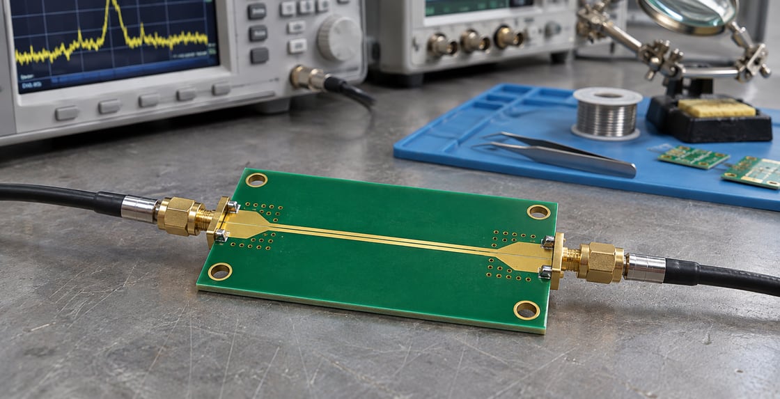
Check Impedance and Loss Separately
Impedance verification can reveal a mismatch but does not replace a frequency-domain loss assessment. Define the acceptance goal before deciding which measurement is sufficient. See the BestPCBs impedance control guide for the wider stackup and coupon requirements.
Put the Mask Decision in the Release Data
Record which sections are covered, where the opening begins and ends, and which dimensions or test structures confirm it. If a change affects assembly, involve the responsible engineer rather than removing mask as a fabrication-only correction.
Request an RF Stackup Review
Share the frequency range and marked mask geometry with Best Technology.
FAQ
Does solder mask always lower the impedance?
Replacing air with dielectric generally changes the effective electrical environment, but the practical result depends on the geometry and actual coverage. Compare the two constructions using appropriate inputs and a representative test. Do not use a fixed correction factor from a different board or transmission line.
Does the mask above the trace matter more than the gap?
That depends on the field distribution of the structure. A coplanar line has fields in the lateral gap as well as beneath and around the trace. Include the actual coverage in the model rather than assuming that only the coating directly over the signal matters.
Is bare copper the same as an open solder mask window?
No. An open window removes mask from an area, but the copper can still have a specified surface finish. Model or measure the construction as it will actually be delivered. Check assembly, handling and environmental needs before choosing how that area should be exposed.
Can I use the same coupon for a masked and unmasked route?
Only if the coupon arrangement actually represents both cases and the acceptance method distinguishes them. A single uniform structure cannot demonstrate the effect of two different coverages. Define the relevant dimensions, mask pattern and test objective before requesting the coupon from the fabricator.
Can I remove mask from an entire RF board?
Do not assume that is necessary or appropriate. Focus on the sections where the electrical performance requires a change, then review assembly, finish and handling needs. A targeted opening can be easier to verify than a blanket removal that creates new constraints elsewhere.
Does passing a 50-ohm check prove low loss?
No. Characteristic impedance and attenuation are related design considerations but are not the same result. A matched line can still have conductor or dielectric loss. If loss is a requirement, agree on a frequency-dependent measurement that represents the relevant route and construction.
How do I handle a small local solder mask dam?
Define its location and geometry, and check whether it changes the response at the frequencies of interest. A uniform section model may not capture a local discontinuity. Keep the soldering purpose of the dam visible while comparing electrical alternatives and verifying the selected arrangement.
What should I send to the RF fabricator?
Send the stackup, frequency range, finished line width and gap, mask artwork and relevant performance limits. Mark the connector launch and any mask boundaries separately. Ask which coupon or test demonstrates the uniform line and which evidence covers the transition or actual assembled route.