In a DDR fly-by topology, shared signals such as clock, address and command travel along a route that passes the memory devices in order. The clock therefore reaches each device at a different time. Where supported, write leveling compensates for the clock-to-write-strobe timing difference at each device; it cannot repair a poorly terminated or incorrectly routed signal.
Consider a hypothetical single-rank board with two discrete DDR3 devices. A controller drives the shared clock and command network, and each device has its own data byte lanes in this example. The goal is to review the route and collect evidence before debugging firmware or changing the board.
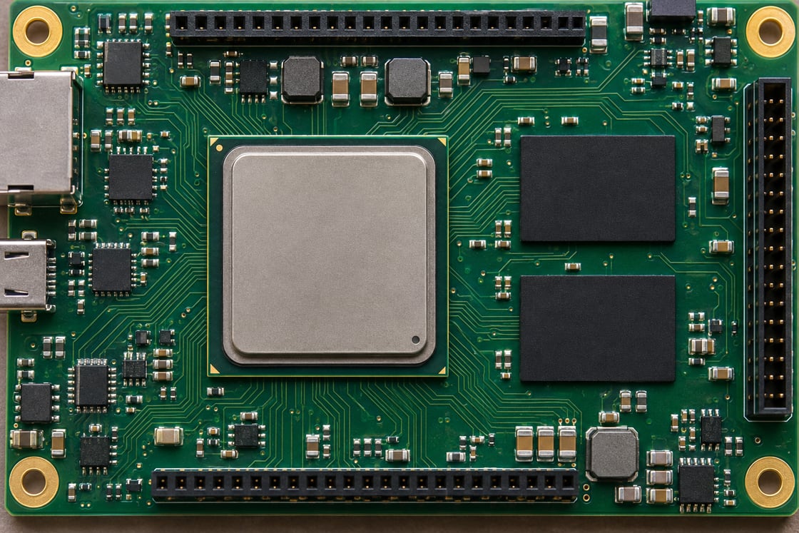
Follow the Clock Past Both Memory Devices
Think of the shared route as one road with two stops. The first receiver sees the edge earlier because its route from the controller is shorter in time. The second sees it later. The receivers do not regenerate the clock for the next device; the PCB interconnect carries it past both loads.
Fly-By vs Balanced T vs Point-to-Point
These topologies distribute a signal in different ways, and the controller documentation determines which is allowed for a particular group. Matching all loads to the same delay is not automatically the design goal on a fly-by net.
| Topology | Routing shape | Key check |
| Fly-by | Receivers along a shared route | Local timing at each load and far-end treatment |
| Balanced T | Branches arranged for similar delays | Branch matching and reflections at the junction |
| Point-to-point | One route between two endpoints | Endpoint timing and reference continuity |
Map Each Signal Group Before Routing
Make a routing table from the controller and memory documentation. For this example, CK means the clock pair, CA refers to command and address, DQ carries data, and DQS is the strobe used to time the data. Check control signals separately instead of assuming that every non-data pin belongs on one shared route.
Build a Timing Budget in Picoseconds
Use delays at the receiver pins rather than simply comparing whole-net lengths. The following values are invented to demonstrate the calculation, not electrical limits. A board-specific budget must include the applicable controller and DRAM rules, package delays where required, and actual routing geometry.
| Illustrative parameter | Device A | Device B |
| CK path delay | 180 ps | 330 ps |
| Write DQS path delay | 200 ps | 220 ps |
| DQS minus CK path delay | +20 ps | −110 ps |
| Relative difference between locations | Baseline | 130 ps earlier relative to local CK |
The example assumes simultaneous launch for the arithmetic only. It does not calculate the real phase at the receiver, a training register value, or compliance margin.
Match Shared Signals at Each Receiver
Check the controller-to-A segment and the controller-to-B segment separately using the constraints for the signal group. A report that ends at the last termination can hide mismatches at A. Export a source-to-load delay report with named endpoints and verify which trace and via segments are included.
Keep Data Lane Checks Separate From Fly-By Checks
In this single-rank example each data lane is reviewed against its own strobe. Do not route DQ along the address chain or assume that a length match between two different byte lanes proves that either lane is valid. Use the lane mapping and timing constraints for the actual controller.
Place Termination for the Route You Actually Built
Follow the device-specific termination scheme and place the far-end elements where the approved topology calls for them. A resistor footprint is not enough: review the stub from the main route, the return path and the termination rail where applicable. Clock and single-ended command signals may require different termination arrangements.
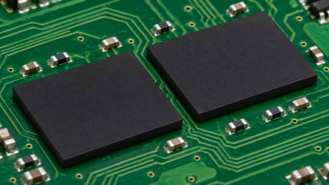
Check the Return Path Through Layer Changes
Check every reference transition as well as trace length. A via or plane gap can change the return-current path and create a discontinuity that the length report does not show. Review layers and references with the approved stackup before tuning; then evaluate the resulting interconnect with the tools and models specified for the interface.
What Write Leveling Changes
Write leveling adjusts the timing of the write strobe relative to the clock observed by the receiving memory. In the AMD PG150 example, the controller drives DQS and the memory returns feedback on DQ during calibration. The output is a controller timing adjustment, not a change to the PCB routing.
What Write Leveling Cannot Fix
Training is not a cure for invalid pin mapping, a missing reference path, a noncompliant termination, or excessive distortion. If the required correction is outside what the specific controller can train, a board can also fail despite having the intended topology. Check supported settings and ranges before interpreting a failure as a layout defect.
Use Failure Patterns to Narrow the First Debug Step
Start with the failing lane or rank, not a new board revision. A failure isolated to one byte lane suggests checking that lane’s mapping, strobe and assembly first; a shared failure across devices also warrants reviewing clock, reset, power and configuration. These are starting points, not proven causes. Save the training logs and compare with the released design.
Release With Routing and Bring-Up Evidence
Keep the routing constraints, per-load delay report, approved stackup, topology and termination notes together. Then record the hardware and firmware revisions used for bring-up and run the approved memory validation at the intended operating conditions. A successful boot is useful evidence, but it does not prove timing margin across the product’s operating range.
FAQ
Can both devices have the same full trace length?
That is not the normal objective for a clock that passes the devices sequentially. Focus on the required local relationship at each receiver and on the controller’s allowable path delays. Adding length just to equalize unrelated endpoints can introduce geometry and delay that the routing guide never requested.
How do I measure only the first section of a fly-by net?
Define the controller and first receiver as the endpoints in a tool that supports source-to-load or pin-pair reporting. Then compare the reported path against the actual route. If the tool reports only total net length, extract the relevant segments explicitly rather than tuning against the length to the terminator.
Does a far-end resistor go on every signal?
No. Use the termination scheme required by the controller, memory and topology. The clock pair, shared single-ended signals, and data lanes can use different arrangements. Read the schematic and layout sections together because placement, connection and electrical value can all affect how a termination works.
Does write leveling replace read training?
No. They address different signal directions and timing relationships. The exact calibration sequence depends on the controller and memory. If the system passes one stage but fails another, record the actual failing stage before deciding which signals to inspect or which configuration to change.
Does a single DRAM device always need fly-by routing?
No multi-device chain is present when there is only one load on that particular net. However, use the approved topology and termination for the selected controller, device and rank arrangement. The number of packages by itself does not define the number of electrical loads on every signal.
Can I copy DDR3 constraints to a DDR4 board?
Do not copy them as a set. A similar topology name does not establish equivalent pin assignments, electrical requirements or allowable timing. Start from the target controller’s documentation for the exact memory interface, then check the memory data sheet and the proposed stackup before importing constraints.
Can a fabricated impedance coupon prove the memory interface works?
No. A coupon can provide evidence about the specified transmission-line construction under its test conditions. It does not measure the assembled receiver timing, lane mapping, connector behavior, or training range. Use it alongside the design review and assembled-board validation, not instead of them.
What does it mean when a board passes once but fails on a cold boot?
It shows an intermittent or condition-dependent symptom, not the root cause. Save the actual test conditions and failing training stage. Compare repeatable cold and warm runs with approved instrumentation and configuration, then investigate candidate issues such as timing margin, rail startup, or assembly rather than discarding the failing log.
References
AMD UG586: DDR3 component routing; AMD PG150: write leveling calibration. For related stackup questions see the Best Technology microstrip PCB guide.
Prepare a Stackup and Routing Review
Send the target interface, routing layers, controlled impedance requirements, and layout revision to sales@bestpcbs.com for a project-specific review request.
You may also like




Tags: DDR fly-by topology, DDR routing, Signal Integrity, write leveling